ICGOO在线商城 > TPS77001DBVT
 Datasheet下载
- 型号: TPS77001DBVT
- 制造商: Texas Instruments
- 库位|库存: xxxx|xxxx
- 要求:
| 数量阶梯 | 香港交货 | 国内含税 |
| +xxxx | $xxxx | ¥xxxx |
查看当月历史价格
查看今年历史价格
TPS77001DBVT产品简介:
ICGOO电子元器件商城为您提供TPS77001DBVT由Texas Instruments设计生产,在icgoo商城现货销售,并且可以通过原厂、代理商等渠道进行代购。 提供TPS77001DBVT价格参考以及Texas InstrumentsTPS77001DBVT封装/规格参数等产品信息。 你可以下载TPS77001DBVT参考资料、Datasheet数据手册功能说明书, 资料中有TPS77001DBVT详细功能的应用电路图电压和使用方法及教程。
| 参数 | 数值 |
| 产品目录 | 集成电路 (IC)半导体 |
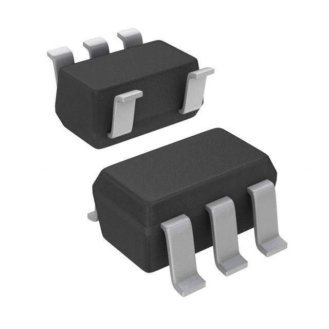
| 描述 | IC REG LDO ADJ 50MA SOT23-5低压差稳压器 Adj 50mA LDO |
| 产品分类 | |
| 品牌 | Texas Instruments |
| 产品手册 | |
| 产品图片 |
|
| rohs | 符合RoHS无铅 / 符合限制有害物质指令(RoHS)规范要求 |
| 产品系列 | 电源管理 IC,低压差稳压器,Texas Instruments TPS77001DBVT- |
| 数据手册 | |
| 产品型号 | TPS77001DBVT |
| PCN设计/规格 | |
| 产品目录页面 | |
| 产品种类 | 低压差稳压器 |
| 供应商器件封装 | SOT-23-5 |
| 其它名称 | 296-2762-6 |
| 包装 | Digi-Reel® |
| 单位重量 | 13 mg |
| 参考电压 | 1.224 V |
| 商标 | Texas Instruments |
| 回动电压—最大值 | 115 mV |
| 安装类型 | 表面贴装 |
| 安装风格 | SMD/SMT |
| 封装 | Reel |
| 封装/外壳 | SC-74A,SOT-753 |
| 封装/箱体 | SOT-23-5 |
| 工作温度 | -40°C ~ 125°C |
| 工厂包装数量 | 250 |
| 最大功率耗散 | 0.555 W |
| 最大工作温度 | + 125 C |
| 最大输入电压 | 10 V |
| 最小工作温度 | - 40 C |
| 最小输入电压 | + 2.7 V |
| 标准包装 | 1 |
| 电压-跌落(典型值) | 0.048V @ 50mA |
| 电压-输入 | 2.7 V ~ 10 V |
| 电压-输出 | 1.2 V ~ 5.5 V |
| 电压调节准确度 | 3 % |
| 电流-输出 | 50mA |
| 电流-限制(最小值) | - |
| 稳压器拓扑 | 正,可调式 |
| 稳压器数 | 1 |
| 系列 | TPS77001 |
| 线路调整率 | 0.04 % / V |
| 负载调节 | 8 mV |
| 输入偏压电流—最大 | 0.017 mA |
| 输出电压 | 1.2 V to 5.5 V |
| 输出电流 | 50 mA |
| 输出端数量 | 1 Output |
| 输出类型 | Adjustable |
| 配用 | /product-detail/zh/TPS76XXXEVM-125/296-11042-ND/381857/product-detail/zh/DEM-SOT23LDO/296-20843-ND/1216448 |


- 商务部:美国ITC正式对集成电路等产品启动337调查
- 曝三星4nm工艺存在良率问题 高通将骁龙8 Gen1或转产台积电
- 太阳诱电将投资9.5亿元在常州建新厂生产MLCC 预计2023年完工
- 英特尔发布欧洲新工厂建设计划 深化IDM 2.0 战略
- 台积电先进制程称霸业界 有大客户加持明年业绩稳了
- 达到5530亿美元!SIA预计今年全球半导体销售额将创下新高
- 英特尔拟将自动驾驶子公司Mobileye上市 估值或超500亿美元
- 三星加码芯片和SET,合并消费电子和移动部门,撤换高东真等 CEO
- 三星电子宣布重大人事变动 还合并消费电子和移动部门
- 海关总署:前11个月进口集成电路产品价值2.52万亿元 增长14.8%


PDF Datasheet 数据手册内容提取
TPS77001, TPS77012, TPS77015, TPS77018, TPS77025 TPS77027, TPS77028, TPS77030, TPS77033, TPS77050 ULTRALOW-POWER 50-mA LOW-DROPOUT LINEAR REGULATORS SLVS210D – JUNE 1999 – REVISED MAY 2001 (cid:0) 50-mA Low-Dropout Regulator DBV PACKAGE (cid:0) (TOP VIEW) Available in 1.2-V, 1.5-V, 1.8-V, 2.5-V, 2.7-V, 2.8-V, 3.0-V, 3.3-V, and 5-V Fixed-Output and IN 1 5 OUT Adjustable Versions (cid:0) Only 17 µA Quiescent Current at 50 mA GND 2 (cid:0) 1 µA Quiescent Current in Standby Mode (cid:0) EN 3 4 NC/FB Dropout Voltage Typically 35 mV at 50 mA (cid:0) Over Current Limitation (cid:0) –40°C to 125°C Operating Junction TPS77033 Temperature Range GROUND CURRENT (cid:0) vs 5-Pin SOT-23 (DBV) Package FREE-AIR TEMPERATURE 22 description VI = 4.3 V The TPS770xx family of low-dropout (LDO) 21 CO = 4.7 µF voltage regulators offers the benefits of low dropout voltage, ultralow-power operation, and 20 miniaturized packaging. These regulators feature A µ low dropout voltages and ultralow quiescent – current compared to conventional LDO nt 19 e r regulators. Offered in a 5-terminal small outline Cur IO = 50 mA IO = 0 mA integrated-circuit SOT-23 package, the d 18 n TPS770xx series devices are ideal for u o micropower operations and where board space is Gr 17 at a premium. A combination of new circuit design and process 16 innovation has enabled the usual PNP pass transistor to be replaced by a PMOS pass 15 element. Because the PMOS pass element –60 –40 –20 0 20 40 60 80 100 120 140 behaves as a low-value resistor, the dropout TA – Free-Air Temperature – °C voltage is very low — typically 35 mV at 50 mA of load current (TPS77050) — and is directly proportional to the load current. Since the PMOS pass element is a voltage-driven device, the quiescent current is ultralow (28 µA maximum) and is stable over the entire range of output load current (0 mA to 50 mA). Intended for use in portable systems such as laptops and cellular phones, the ultralow-dropout voltage feature and ultralow-power operation result in a significant increase in system battery operating life. The TPS770xx also features a logic-enabled sleep mode to shut down the regulator, reducing quiescent current to 1 µA typical at T = 25°C. The TPS770xx is offered in 1.2-V, 1.5-V, 1.8-V, 2.5-V, 2.7-V, 2.8-V, 3.0-V, 3.3-V, J and 5-V fixed-voltage versions and in a variable version (programmable over the range of 1.2 V to 5.5 V). Please be aware that an important notice concerning availability, standard warranty, and use in critical applications of TexasInstruments semiconductor products and disclaimers thereto appears at the end of this data sheet. PRODUCTION DATA information is current as of publication date. Copyright 2001, Texas Instruments Incorporated Products conform to specifications per the terms of Texas Instruments standard warranty. Production processing does not necessarily include testing of all parameters. POST OFFICE BOX 655303 • DALLAS, TEXAS 75265 1
TPS77001, TPS77012, TPS77015, TPS77018, TPS77025 TPS77027, TPS77028, TPS77030, TPS77033, TPS77050 ULTRALOW-POWER 50-mA LOW-DROPOUT LINEAR REGULATORS SLVS210D – JUNE 1999 – REVISED MAY 2001 AVAILABLE OPTIONS TJ VOLTAGE PACKAGE PART NUMBER SYMBOL Variable TPS77001DBVT† TPS77001DBVR‡ PCPI 1.2V to 5.5V 1.2 V TPS77012DBVT† TPS77012DBVR‡ PCQI 1.5 V TPS77015DBVT† TPS77015DBVR‡ PCRI 1.8 V TPS77018DBVT† TPS77018DBVR‡ PCSI –40°C to 125°C 2.5 V SOT-23 TPS77025DBVT† TPS77025DBVR‡ PCTI ((DDBBVV)) 2.7 V TPS77027DBVT† TPS77027DBVR‡ PCUI 2.8 V TPS77028DBVT† TPS77028DBVR‡ PCVI 3.0 V TPS77030DBVT† TPS77030DBVR‡ PCWI 3.3 V TPS77033DBVT† TPS77033DBVR‡ PCXI 5.0 V TPS77050DBVT† TPS77050DBVR‡ PCYI †The DBVT indicates tape and reel of 250 parts. ‡The DBVR indicates tape and reel of 3000 parts. functional block diagram TPS77001 IN OUT EN Current Limit / Thermal VREF Protection FB GND TPS77012/15/18/25/27/28/30/33/50 IN OUT EN Current Limit / Thermal VREF Protection GND 2 POST OFFICE BOX 655303 • DALLAS, TEXAS 75265
TPS77001, TPS77012, TPS77015, TPS77018, TPS77025 TPS77027, TPS77028, TPS77030, TPS77033, TPS77050 ULTRALOW-POWER 50-mA LOW-DROPOUT LINEAR REGULATORS SLVS210D – JUNE 1999 – REVISED MAY 2001 Terminal Functions TERMINAL II//OO DDEESSCCRRIIPPTTIIOONN NAME NO. GND 2 Ground EN 3 I Enable input FB 4 I Feedback voltage (TPS77001 only) IN 1 I Input supply voltage NC 4 No connection (Fixed options only) OUT 5 O Regulated output voltage absolute maximum ratings over operating free-air temperature range (unless otherwise noted)(cid:0) Input voltage range(cid:1)(cid:7)(cid:5)(cid:5)(cid:4)(cid:6)(cid:8)(cid:5)(cid:3)(cid:2) . . . . . . . . . . . . . . . . . . . . . . . . . . . . . . . . . . . . . . . . . . . . . . . . . . –0.3 V to 13.5 V Voltage range at EN . . . . . . . . . . . . . . . . . . . . . . . . . . . . . . . . . . . . . . . . . . . . . . . . . . . . . . . . . . . –0.3 V to V + 0.3 V I Voltage on OUT, FB. . . . . . . . . . . . . . . . . . . . . . . . . . . . . . . . . . . . . . . . . . . . . . . . . . . . . . . . . . . . . . . . . . . . . . . . . . 7 V Peak output current . . . . . . . . . . . . . . . . . . . . . . . . . . . . . . . . . . . . . . . . . . . . . . . . . . . . . . . . . . . . . . Internally limited ESD rating, HBM . . . . . . . . . . . . . . . . . . . . . . . . . . . . . . . . . . . . . . . . . . . . . . . . . . . . . . . . . . . . . . . . . . . . . . . . . . 2 kV Continuous total power dissipation . . . . . . . . . . . . . . . . . . . . . . . . . . . . . . . . . . . . . See Dissipation Rating Table Operating virtual junction temperature range, T . . . . . . . . . . . . . . . . . . . . . . . . . . . . . . . . . . . . . –40°C to 150°C J Storage temperature range, T . . . . . . . . . . . . . . . . . . . . . . . . . . . . . . . . . . . . . . . . . . . . . . . . . . . –65°C to 150°C stg †Stresses beyond those listed under “absolute maximum ratings” may cause permanent damage to the device. These are stress ratings only, and functional operation of the device at these or any other conditions beyond those indicated under “recommended operating conditions” is not implied. Exposure to absolute-maximum-rated conditions for extended periods may affect device reliability. NOTE 1: All voltage values are with respect to network ground terminal. DISSIPATION RATING TABLE DERATING FACTOR TA ≤ 25°C TA = 70°C TA = 85°C BOARD PACKAGE RθJC RθJA ABOVE TA = 25°C POWER RATING POWER RATING POWER RATING Low K‡ DBV 65.8 °C/W 259 °C/W 3.9 mW/°C 386 mW 212 mW 154 mW High K§ DBV 65.8 °C/W 180 °C/W 5.6 mW/°C 555 mW 305 mW 222 mW ‡The JEDEC Low K (1s) board design used to derive this data was a 3 inch x 3 inch, two layer board with 2 ounce copper traces on top of the board. §The JEDEC High K (2s2p) board design used to derive this data was a 3 inch x 3 inch, multilayer board with 1 ounce internal power and ground planes and 2 ounce copper traces on top and bottom of the board. recommended operating conditions MIN NOM MAX UNIT Input voltage, VI (see Note 2) 2.7 10 V Output voltage range, VO 1.2 5.5 V Continuous output current, IO (see Note 3) 0 50 mA Operating junction temperature, TJ –40 125 °C NOTES: 2. To calculate the minimum input voltage for your maximum output current, use the following formula: VI(min) = VO(max) + VDO (max load) 3. Continuous output current and operating junction temperature are limited by internal protection circuitry, but it is not recommended that the device operate under conditions beyond those specified in this table for extended periods of time. POST OFFICE BOX 655303 • DALLAS, TEXAS 75265 3
TPS77001, TPS77012, TPS77015, TPS77018, TPS77025 TPS77027, TPS77028, TPS77030, TPS77033, TPS77050 ULTRALOW-POWER 50-mA LOW-DROPOUT LINEAR REGULATORS SLVS210D – JUNE 1999 – REVISED MAY 2001 electrical characteristics over recommended operating free–air temperature range, µ VI = VO(typ) + 1 V, IO = 50 mA, EN = 0V, Co = 4.7 F (unless otherwise noted) PARAMETER TEST CONDITIONS MIN TYP MAX UNIT 1.2 V ≤ VO ≤ 5.5 V, TJ = 25°C VO TTPPSS7777000011 1.2 V ≤ VO ≤ 5.5 V, TJ = –40°C to 125°C 0.97VO 1.03VO TJ = 25°C, 2.7 V < VIN < 10 V 1.224 TTPPSS7777001122 TJ = –40°C to 125°C, 2.7 V < VIN < 10 V 1.187 1.261 TJ = 25°C, 2.7 V < VIN < 10 V 1.5 TTPPSS7777001155 TJ = –40°C to 125°C, 2.7 V < VIN < 10 V 1.455 1.545 TJ = 25°C, 2.8 V < VIN < 10 V 1.8 TTPPSS7777001188 TJ = –40°C to 125°C, 2.8 V < VIN < 10 V 1.746 1.854 TJ = 25°C, 3.5 V < VIN < 10 V 2.5 TTPPSS7777002255 Output voltagge ((10 µµA to 50 mA load)) TJ = –40°C to 125°C, 3.5 V < VIN < 10 V 2.425 2.575 VV (see Note 4) TJ = 25°C, 3.7 V < VIN < 10 V 2.7 TTPPSS7777002277 TJ = –40°C to 125°C, 3.7 V < VIN < 10 V 2.619 2.781 TJ = 25°C, 3.8 V < VIN < 10 V 2.8 TTPPSS7777002288 TJ = –40°C to 125°C, 3.8 V < VIN < 10 V 2.716 2.884 TJ = 25°C, 4.0 V < VIN < 10 V 3.0 TTPPSS7777003300 TJ = –40°C to 125°C, 4.0 V < VIN < 10 V 2.910 3.090 TJ = 25°C, 4.3 V < VIN < 10 V 3.3 TTPPSS7777003333 TJ = –40°C to 125°C, 4.3 V < VIN < 10 V 3.201 3.399 TJ = 25°C, 6.0 V < VIN < 10 V 5.0 TTPPSS7777005500 TJ = –40°C to 125°C, 6.0 V < VIN < 10 V 4.850 5.150 EN = 0V, 0 mA < IO < 50mA, 17 TJ = 25°C QQuuiieesscceenntt ccuurrrreenntt ((GGNNDD ccuurrrreenntt)) ((sseeee NNoottee 44)) µµAA EN = 0V, IO = 50mA, 28 TJ = –40°C to 125°C VO + 1 V < VI ≤ 10 V, TJ = 25°C 0.04 OOuuttppuutt vvoollttaaggee lliinnee rreegguullaattiioonn ((∆∆VVOO//VVOO)) (see Notes 4 and 5) VO + 1 V < VI ≤ 10 V, 0.1 %/V TJ = –40°C to 125°C EN = 0V, IO = 0 to 50 mA, Load regulation 8 mV TJ = 25°C BW = 300 Hz to 50 kHz, Output noise voltage 190 µVrms Co = 10 µF, TJ = 25°C Output current limit VO = 0V, See Note 4 350 750 mA EN = VI, 2.7 < VI < 10 V 1 µA SSttaannddbbyy ccuurrrreenntt TJ = –40°C to 125°C 2 µA NOTES: 4. Minimum IN operating voltage is 2.7 V or VO (typ) + 1 V, whichever is greater. Maximum IN voltage 10 V, minimum output current 10 µA, maximum output current 50 mA. 5. If VO≤ 1.8 V then VImin = 2.7 V, VImax = 10 V: VO(cid:5)VImax(cid:2)2.7 V(cid:6) Line Reg. (mV) (cid:3) (cid:5)%(cid:4)V(cid:6) (cid:0) (cid:0)1000 100 If VO≥ 2.5 V then VImin = VO + 1 V, VImax = 10 V: VO(cid:5)VImax(cid:2)(cid:5)VO(cid:1)1 V(cid:6)(cid:6) Line Reg. (mV) (cid:3) (cid:5)%(cid:4)V(cid:6) (cid:0) (cid:0)1000 100 4 POST OFFICE BOX 655303 • DALLAS, TEXAS 75265
TPS77001, TPS77012, TPS77015, TPS77018, TPS77025 TPS77027, TPS77028, TPS77030, TPS77033, TPS77050 ULTRALOW-POWER 50-mA LOW-DROPOUT LINEAR REGULATORS SLVS210D – JUNE 1999 – REVISED MAY 2001 electrical characteristics over recommended operating free–air temperature range, V = V + I O(typ) µ 1 V, IO = 50 mA, EN = 0V, Co = 4.7 F (unless otherwise noted) (continued) PARAMETER TEST CONDITIONS MIN TYP MAX UNIT FB input current FB = 1.224 V (TPS77001) –1 1 µA High level enable input voltage 2.7 V < VI < 10 V 1.7 V Low level enable input voltage 2.7 V < VI < 10 V 0.9 V f = 1 kHz, CO = 10 µF, Power supply ripple rejection 60 dB TJ = 25°C, See Note 4 EN = 0 V –1 0 1 µA IInnppuutt ccuurrrreenntt ((EENN)) EN = VI –1 1 µA IO = 50 mA, TJ = 25°C 60 TTPPSS7777002288 IO = 50 mA TJ = –40°C to 125°C 125 IO = 50 mA, TJ = 25°C 57 TTPPSS7777003300 IO = 50 mA TJ = –40°C to 125°C 115 DDrrooppoouutt vvoollttaaggee ((sseeee NNoottee 66)) mmVV IO = 50 mA, TJ = 25°C 48 TTPPSS7777003333 IO = 50 mA TJ = –40°C to 125°C 100 IO = 50 mA, TJ = 25°C 35 TTPPSS7777005500 IO = 50 mA TJ = –40°C to 125°C 85 NOTES: 4. Minimum IN operating voltage is 2.7 V or VO (typ) + 1 V, whichever is greater. Maximum IN voltage 10 V, minimum output current 10 µA, maximum output current 50 mA. 6. IN voltage equals VO(Typ) –100mV; TPS77001 output voltage set to 3.3 V nominal with external resistor divider. TPS77012, TPS77015, TPS77018, TPS77025, and TPS77027 dropout voltage limited by input voltage range limitations. TYPICAL CHARACTERISTICS Table of Graphs FIGURE vs Output current 1, 2, 3 VVOO OOuuttppuutt vvoollttaaggee vs Free-air temperature 4, 5, 6 Ground current vs Free-air temperature 7 Output spectral noise density vs Frequency 8 Zo Output impedance vs Frequency 9 VDO Dropout voltage vs Free-air temperature 10 Ripple rejection vs Frequency 11 LDO startup time 12 Line transient response 13, 15 Load transient response 14, 16 vs Output current 17, 19 EEqquuiivvaalleenntt sseerriieess rreessiissttaannccee ((EESSRR)) vs Added ceramic capacitance 18, 20 POST OFFICE BOX 655303 • DALLAS, TEXAS 75265 5
TPS77001, TPS77012, TPS77015, TPS77018, TPS77025 TPS77027, TPS77028, TPS77030, TPS77033, TPS77050 ULTRALOW-POWER 50-mA LOW-DROPOUT LINEAR REGULATORS SLVS210D – JUNE 1999 – REVISED MAY 2001 TYPICAL CHARACTERISTICS TPS77025 TPS77015 OUTPUT VOLTAGE OUTPUT VOLTAGE vs vs OUTPUT CURRENT OUTPUT CURRENT 2.498 1.498 2.496 TVCAIO = == 3 2.455. 7°V CµF 1.496 TVCAIO = == 2 2.475. 7°V CµF 2.494 1.494 V V Voltage – 22..449902 Voltage – 1.492 Output 2.488 Output 1.490 – O – O 1.488 V 2.486 V 1.486 2.484 2.482 1.484 0 10 20 30 40 50 0 10 20 30 40 50 IO – Output Current – mA IO – Output Current – mA Figure 1 Figure 2 TPS77033 TPS77015 OUTPUT VOLTAGE OUTPUT VOLTAGE vs vs OUTPUT CURRENT FREE-AIR TEMPERATURE 3.284 1.496 VI = 4.3 V CO = 4.7 µF 1.494 3.282 TA = 25°C IO = 1 mA VI = 2.7 V 1.492 CO = 4.7 µF Output Voltage – V 333...222877086 Output Voltage – V 111...444889680 V– O 3.274 V– O1.484 IO = 50 mA 3.272 1.482 3.270 1.480 0 10 20 30 40 50 –60 –40 –20 0 20 40 60 80 100 120 140 IO – Output Current – mA TA – Free-Air Temperature – °C Figure 3 Figure 4 6 POST OFFICE BOX 655303 • DALLAS, TEXAS 75265
TPS77001, TPS77012, TPS77015, TPS77018, TPS77025 TPS77027, TPS77028, TPS77030, TPS77033, TPS77050 ULTRALOW-POWER 50-mA LOW-DROPOUT LINEAR REGULATORS SLVS210D – JUNE 1999 – REVISED MAY 2001 TYPICAL CHARACTERISTICS TPS77025 TPS77033 OUTPUT VOLTAGE OUTPUT VOLTAGE vs vs FREE-AIR TEMPERATURE FREE-AIR TEMPERATURE 2.496 3.285 VI = 4.3 V 2.494 CO = 4.7 µF IO = 1 mA 3.280 IO = 1 mA 2.492 V 2.490 V – – 3.275 e e g 2.488 g a a olt olt ut V 2.486 IO = 50 mA ut V 3.270 IO = 50 mA p p ut 2.484 ut O O – – 3.265 O2.482 O V V 2.480 3.260 2.478 VI = 3.5 V CO = 4.7 µF 2.476 3.255 –60 –40 –20 0 20 40 60 80 100 120 140 –60 –40 –20 0 20 40 60 80 100 120 140 TA – Free-Air Temperature – °C TA – Free-Air Temperature – °C Figure 5 Figure 6 TPS77033 TPS77033 GROUND CURRENT OUTPUT SPECTRAL NOISE DENSITY vs vs FREE-AIR TEMPERATURE FREQUENCY 22 2 VI = 4.3 V z 1.8 21 CO = 4.7 µF VH 1.6 CO = 10 µF µ IO = 1 mA µA 20 sity – 1.4 CIOO = = 5 40. 7m µAF nt – 19 Den 1.2 e e Curr IO = 50 mA IO = 0 mA Nois 1 Ground 1187 pectral 00..68 CIOO = = 1 4 m.7A µF S ut 0.4 p 16 ut O 0.2 CO = 10 µF VI = 4.3 V IO = 50 mA 15 0 –60 –40 –20 0 20 40 60 80 100 120 140 100 1k 10k 100k TA – Free-Air Temperature – °C f – Frequency – Hz Figure 7 Figure 8 POST OFFICE BOX 655303 • DALLAS, TEXAS 75265 7
TPS77001, TPS77012, TPS77015, TPS77018, TPS77025 TPS77027, TPS77028, TPS77030, TPS77033, TPS77050 ULTRALOW-POWER 50-mA LOW-DROPOUT LINEAR REGULATORS SLVS210D – JUNE 1999 – REVISED MAY 2001 TYPICAL CHARACTERISTICS TPS77033 OUTPUT IMPEDANCE DROPOUT VOLTAGE vs vs FREQUENCY FREE-AIR TEMPERATURE 100 2 VI = 4.3 V VI = 3.2 V 1.8 CO = 4.7 µF CO = 4.7 µF 1.6 IO = 50 mA Ω V m ce – 1.4 e – n g a 1.2 a ed olt p V 10 ut Im 1 pout p 0.8 o – Out 0.6 IO = 1 mA – DrO IO = 10 mA Zo VD 0.4 IO = 50 mA 0.2 0 1 10 100 1k 10k 100k 1M –60 –40 –20 0 20 40 60 80 100 120 140 f – Frequency – Hz TA – Free-Air Temperature – °C Figure 9 Figure 10 TPS77033 RIPPLE REJECTION vs LDO STARTUP TIME FREQUENCY 100 90 80 EN 70 B d – 60 IO = 1 mA n o cti 50 e ej R 40 e pl 30 p Ri 20 IO = 50 mA 10 VCIO = = 4 .43. 7V µF VO 0 ESR = 0.3 Ω –10 10 100 1 k 10 k 100 k 1 M 10 M 0 20 40 60 80 100 120 140 160 180 200 f – Frequency – Hz t – Time – µs Figure 11 Figure 12 8 POST OFFICE BOX 655303 • DALLAS, TEXAS 75265
TPS77001, TPS77012, TPS77015, TPS77018, TPS77025 TPS77027, TPS77028, TPS77030, TPS77033, TPS77050 ULTRALOW-POWER 50-mA LOW-DROPOUT LINEAR REGULATORS SLVS210D – JUNE 1999 – REVISED MAY 2001 TYPICAL CHARACTERISTICS TPS77015 TPS77015 LINE TRANSIENT RESPONSE LOAD TRANSIENT RESPONSE V m – A e m ag 10 – 50 Volt oad put 0 nt L Out rre – –10 Cu 0 O V 3.7 V V m – Input Voltage – 2.7 ICELSO =R =1 = 04 0.m7.3 Aµ ΩF – Change In Output Voltage – ––150000 VCEISO =R = 2= .17 00 V. µ3 FΩ VI O V 0 20 40 60 80 100 120 140 160 180 200 ∆ 0 20 40 60 80 100 120 140 160 180 200 t – Time – µs t – Time – µs Figure 13 Figure 14 TPS77033 TPS77033 LINE TRANSIENT RESPONSE LOAD TRANSIENT RESPONSE V m – A e m ag 10 – 50 Volt oad put 0 nt L Out rre – –10 Cu 0 O V V 5.3 m – V e – g 0 Voltage 4.3 ange In ut Volta –20 ut IL = 10 mA Ch utp VI = 4.3 V – Inp ECSOR = = 4 0.7.3 µ ΩF – VO O –40 ECSOR = = 4 0.7.3 µ ΩF VI ∆ 0 20 40 60 80 100 120 140 160 180 0 20 40 60 80 100 120 140 160 180 t – Time – µs t – Time – µs Figure 15 Figure 16 POST OFFICE BOX 655303 • DALLAS, TEXAS 75265 9
TPS77001, TPS77012, TPS77015, TPS77018, TPS77025 TPS77027, TPS77028, TPS77030, TPS77033, TPS77050 ULTRALOW-POWER 50-mA LOW-DROPOUT LINEAR REGULATORS SLVS210D – JUNE 1999 – REVISED MAY 2001 TYPICAL CHARACTERISTICS TPS77033 TPS77033 TYPICAL REGIONS OF STABILITY TYPICAL REGIONS OF STABILITY EQUIVALENT SERIES RESISTANCE (ESR)† EQUIVALENT SERIES RESISTANCE (ESR) vs vs OUTPUT CURRENT ADDED CERAMIC CAPACITANCE 100 100 VIN = 4.3 V VIN = 4.3 V Ωe – ECSOR = = 4 0.7.3 µ ΩF Ωe – ICLO = =5 04 .m7 AµF nc 3.3 V LDO nc a a st Region of Instability st si 10 si e e R R s s e e Region of Instability ri ri Se Se 10 nt nt e e al al uiv 1 uiv q q E E – Region of Stability – Region of Stability R R S S E E 0.1 1 0 5 10 15 20 25 30 35 40 45 50 0 0.1 0.2 0.3 0.4 0.5 0.6 0.7 0.8 0.9 1 IO – Output Current – mA Added Ceramic Capacitance – µF Figure 17 Figure 18 TPS77033 TPS77033 TYPICAL REGIONS OF STABILITY TYPICAL REGIONS OF STABILITY EQUIVALENT SERIES RESISTANCE (ESR)† EQUIVALENT SERIES RESISTANCE (ESR) vs vs OUTPUT CURRENT ADDED CERAMIC CAPACITANCE 100 100 VIN = 4.3 V VIN = 4.3 V Ωe – ECSOR = = 1 00. µ3 FΩ Ωe – ICLO = =5 01 0m µAF nc 3.3 V LDO nc a Region of Instability a st st si si e e R R s s e e Region of Instability ri ri Se 10 Se 10 ent Region of Stability ent al al v v ui ui q q E E – – Region of Stability R R S S E E 1 1 0 5 10 15 20 25 30 35 40 45 50 0 0.1 0.2 0.3 0.4 0.5 0.6 0.7 0.8 0.9 1 IO – Output Current – mA Added Ceramic Capacitance – µF Figure 19 Figure 20 10 POST OFFICE BOX 655303 • DALLAS, TEXAS 75265
TPS77001, TPS77012, TPS77015, TPS77018, TPS77025 TPS77027, TPS77028, TPS77030, TPS77033, TPS77050 ULTRALOW-POWER 50-mA LOW-DROPOUT LINEAR REGULATORS SLVS210D – JUNE 1999 – REVISED MAY 2001 APPLICATION INFORMATION The TPS770xx family of low-dropout (LDO) regulators have been optimized for use in battery-operated equipment. They feature extremely low dropout voltages, low quiescent current (17 µA nominally), and enable inputs to reduce supply currents to less than 1 µA when the regulators are turned off. device operation The TPS770xx uses a PMOS pass element to dramatically reduce both dropout voltage and supply current over more conventional PNP-pass-element LDO designs. The PMOS pass element is a voltage-controlled device and, unlike a PNP transistor, it does not require increased drive current as output current increases. Supply current in the TPS770xx is essentially constant from no load to maximum load. Current limiting and thermal protection prevent damage by excessive output current and/or power dissipation. The device switches into a constant-current mode at approximately 350 mA; further load reduces the output voltage instead of increasing the output current. The thermal protection shuts the regulator off if the junction temperature rises above approximately 165°C. Recovery is automatic when the junction temperature drops approximately 25°C below the high temperature trip point. The PMOS pass element includes a back gate diode that conducts reverse current when the input voltage level drops below the output voltage level. A voltage of 1.7 V or greater on the EN input will disable the TPS770xx internal circuitry, reducing the supply current to 1µA. A voltage of less than 0.9 V on the EN input will enable the TPS770xx and will enable normal operation to resume. The EN input does not include any deliberate hysteresis, and it exhibits an actual switching threshold of approximately 1.5 V. A typical application circuit is shown in Figure 21. TPS770xx† 1 VI IN 4 NC/FB 5 C1 OUT VO 1 µF 3 EN + 4.7 µF GND 2 ESR = 0.2 Ω †TPS77012, TPS77015, TPS77018, TPS77025, TPS77027, TPS77028, TPS77030, TPS77033, TPS77050 (fixed-voltage options). Figure 21. Typical Application Circuit POST OFFICE BOX 655303 • DALLAS, TEXAS 75265 11
TPS77001, TPS77012, TPS77015, TPS77018, TPS77025 TPS77027, TPS77028, TPS77030, TPS77033, TPS77050 ULTRALOW-POWER 50-mA LOW-DROPOUT LINEAR REGULATORS SLVS210D – JUNE 1999 – REVISED MAY 2001 APPLICATION INFORMATION external capacitor requirements Although not required, a 0.047-µF or larger ceramic input bypass capacitor, connected between IN and GND and located close to the TPS770xx, is recommended to improve transient response and noise rejection. A higher-value electrolytic input capacitor may be necessary if large, fast-rise-time load transients are anticipated and the device is located several inches from the power source. Like all low dropout regulators, the TPS770xx requires an output capacitor connected between OUT and GND to stabilize the internal control loop. The minimum recommended capacitance is 4.7 µF. The ESR (equivalent series resistance) of the capacitor should be between 0.2 Ω and 10 Ω. to ensure stability. Capacitor values larger than 4.7 µF are acceptable, and allow the use of smaller ESR values. Capacitances less than 4.7 µF are not recommended because they require careful selection of ESR to ensure stability. Solid tantalum electrolytic, aluminum electrolytic, and multilayer ceramic capacitors are all suitable, provided they meet the requirements described above. Most of the commercially available 4.7 µF surface-mount solid tantalum capacitors, including devices from Sprague, Kemet, and Nichico, meet the ESR requirements stated above. Multilayer ceramic capacitors may have very small equivalent series resistances and may thus require the addition of a low value series resistor to ensure stability. CAPACITOR SELECTION PART NO. MFR. VALUE MAX ESR† SIZE (H × L × W)† T494B475K016AS KEMET 4.7 µF 1.5 Ω 1.9 × 3.5 × 2.8 195D106x0016x2T SPRAGUE 10 µF 1.5 Ω 1.3 × 7.0 × 2.7 695D106x003562T SPRAGUE 10 µF 1.3 Ω 2.5 × 7.6 × 2.5 TPSC475K035R0600 AVX 4.7 µF 0.6 Ω 2.6 × 6.0 × 3.2 †Size is in mm. ESR is maximum resistance in Ohms at 100 kHz and TA = 25°C. Contact manufacturer for minimum ESR values. 12 POST OFFICE BOX 655303 • DALLAS, TEXAS 75265
TPS77001, TPS77012, TPS77015, TPS77018, TPS77025 TPS77027, TPS77028, TPS77030, TPS77033, TPS77050 ULTRALOW-POWER 50-mA LOW-DROPOUT LINEAR REGULATORS SLVS210D – JUNE 1999 – REVISED MAY 2001 APPLICATION INFORMATION output voltage programming The output voltage of the TPS77001 adjustable regulator is programmed using an external resistor divider as shown in Figure 22. The output voltage is calculated using: VO(cid:3)Vref(cid:0)(cid:4)1(cid:1)RR12(cid:5) (1) where V = 1.224 V typ (the internal reference voltage) ref Resistors R1 and R2 should be chosen for approximately 7-µA divider current. Lower value resistors can be used but offer no inherent advantage and waste more power. Higher values should be avoided as leakage currents at FB increase the output voltage error. The recommended design procedure is to choose R2 = 169kΩ to set the divider current at 7 µA and then calculate R1 using: (cid:4)V (cid:5) O R1(cid:3) (cid:2)1 (cid:0)R2 (2) V ref OUTPUT VOLTAGE PROGRAMMING GUIDE TPS77001 OUTPUT DIVIDER RESISTANCE VOLTAGE (kΩ)‡ 1 (V) R1 R2 VI IN 1 µF 2.5 174 169 5 3.3 287 169 OUT VO ≥1.7 V 3.6 324 169 3 R1 EN 4.0 383 169 4 ≤0.9 V FB 4.7 µF 5.0 523 169 GND ‡1% values shown. 2 R2 ESR = 0.2 Ω Figure 22. TPS77001 Adjustable LDO Regulator Programming POST OFFICE BOX 655303 • DALLAS, TEXAS 75265 13
TPS77001, TPS77012, TPS77015, TPS77018, TPS77025 TPS77027, TPS77028, TPS77030, TPS77033, TPS77050 ULTRALOW-POWER 50-mA LOW-DROPOUT LINEAR REGULATORS SLVS210D – JUNE 1999 – REVISED MAY 2001 APPLICATION INFORMATION power dissipation and junction temperature Specified regulator operation is assured to a junction temperature of 125°C; the maximum junction temperature should be restricted to 125°C under normal operating conditions. This restriction limits the power dissipation the regulator can handle in any given application. To ensure the junction temperature is within acceptable limits, calculate the maximum allowable dissipation, P , and the actual dissipation, P , which must be less than D(max) D or equal to P . D(max) The maximum-power-dissipation limit is determined using the following equation: TJmax(cid:1)TA PD(max)(cid:2) R (cid:0)JA Where: TJmax is the maximum allowable junction temperature RθJA is the thermal resistance junction-to-ambient for the package, see the dissipation rating table. TA is the ambient temperature. The regulator dissipation is calculated using: PD(cid:2)(cid:3)VI(cid:1)VO(cid:4)(cid:0)IO Power dissipation resulting from quiescent current is negligible. Excessive power dissipation will trigger the thermal protection circuit. regulator protection The TPS770xx PMOS-pass transistor has a built-in back diode that conducts reverse current when the input voltage drops below the output voltage (e.g., during power down). Current is conducted from the output to the input and is not internally limited. If extended reverse voltage operation is anticipated, external limiting might be appropriate. The TPS770xx features internal current limiting and thermal protection. During normal operation, the TPS770xx limits output current to approximately 350 mA. When current limiting engages, the output voltage scales back linearly until the overcurrent condition ends. While current limiting is designed to prevent gross device failure, care should be taken not to exceed the power dissipation ratings of the package. If the temperature of the device exceeds approximately 165°C, thermal-protection circuitry shuts it down. Once the device has cooled down to below approximately 140°C, regulator operation resumes. 14 POST OFFICE BOX 655303 • DALLAS, TEXAS 75265
PACKAGE OPTION ADDENDUM www.ti.com 6-Feb-2020 PACKAGING INFORMATION Orderable Device Status Package Type Package Pins Package Eco Plan Lead/Ball Finish MSL Peak Temp Op Temp (°C) Device Marking Samples (1) Drawing Qty (2) (6) (3) (4/5) TPS77001DBVR ACTIVE SOT-23 DBV 5 3000 Green (RoHS NIPDAU Level-1-260C-UNLIM PCPI & no Sb/Br) TPS77001DBVT ACTIVE SOT-23 DBV 5 250 Green (RoHS NIPDAU Level-1-260C-UNLIM PCPI & no Sb/Br) TPS77012DBVR ACTIVE SOT-23 DBV 5 3000 Green (RoHS NIPDAU Level-1-260C-UNLIM PCQI & no Sb/Br) TPS77012DBVT ACTIVE SOT-23 DBV 5 250 Green (RoHS NIPDAU Level-1-260C-UNLIM PCQI & no Sb/Br) TPS77015DBVR ACTIVE SOT-23 DBV 5 3000 Green (RoHS NIPDAU Level-1-260C-UNLIM PCRI & no Sb/Br) TPS77015DBVT ACTIVE SOT-23 DBV 5 250 Green (RoHS NIPDAU Level-1-260C-UNLIM PCRI & no Sb/Br) TPS77018DBVR ACTIVE SOT-23 DBV 5 3000 Green (RoHS NIPDAU Level-1-260C-UNLIM PCSI & no Sb/Br) TPS77018DBVRG4 ACTIVE SOT-23 DBV 5 3000 Green (RoHS NIPDAU Level-1-260C-UNLIM PCSI & no Sb/Br) TPS77018DBVT ACTIVE SOT-23 DBV 5 250 Green (RoHS NIPDAU Level-1-260C-UNLIM PCSI & no Sb/Br) TPS77025DBVR ACTIVE SOT-23 DBV 5 3000 Green (RoHS NIPDAU Level-1-260C-UNLIM PCTI & no Sb/Br) TPS77025DBVRG4 ACTIVE SOT-23 DBV 5 3000 Green (RoHS NIPDAU Level-1-260C-UNLIM PCTI & no Sb/Br) TPS77025DBVT ACTIVE SOT-23 DBV 5 250 Green (RoHS NIPDAU Level-1-260C-UNLIM PCTI & no Sb/Br) TPS77027DBVR ACTIVE SOT-23 DBV 5 3000 Green (RoHS NIPDAU Level-1-260C-UNLIM PCUI & no Sb/Br) TPS77027DBVT ACTIVE SOT-23 DBV 5 250 Green (RoHS NIPDAU Level-1-260C-UNLIM PCUI & no Sb/Br) TPS77028DBVR ACTIVE SOT-23 DBV 5 3000 Green (RoHS NIPDAU Level-1-260C-UNLIM PCVI & no Sb/Br) TPS77028DBVT ACTIVE SOT-23 DBV 5 250 Green (RoHS NIPDAU Level-1-260C-UNLIM PCVI & no Sb/Br) TPS77030DBVR ACTIVE SOT-23 DBV 5 3000 Green (RoHS NIPDAU Level-1-260C-UNLIM PCWI & no Sb/Br) Addendum-Page 1
PACKAGE OPTION ADDENDUM www.ti.com 6-Feb-2020 Orderable Device Status Package Type Package Pins Package Eco Plan Lead/Ball Finish MSL Peak Temp Op Temp (°C) Device Marking Samples (1) Drawing Qty (2) (6) (3) (4/5) TPS77030DBVRG4 ACTIVE SOT-23 DBV 5 3000 Green (RoHS NIPDAU Level-1-260C-UNLIM PCWI & no Sb/Br) TPS77030DBVT ACTIVE SOT-23 DBV 5 250 Green (RoHS NIPDAU Level-1-260C-UNLIM PCWI & no Sb/Br) TPS77030DBVTG4 ACTIVE SOT-23 DBV 5 250 Green (RoHS NIPDAU Level-1-260C-UNLIM PCWI & no Sb/Br) TPS77033DBVR ACTIVE SOT-23 DBV 5 3000 Green (RoHS NIPDAU Level-1-260C-UNLIM -40 to 125 PCXI & no Sb/Br) TPS77033DBVRG4 ACTIVE SOT-23 DBV 5 3000 Green (RoHS NIPDAU Level-1-260C-UNLIM -40 to 125 PCXI & no Sb/Br) TPS77033DBVT ACTIVE SOT-23 DBV 5 250 Green (RoHS NIPDAU Level-1-260C-UNLIM -40 to 125 PCXI & no Sb/Br) TPS77033DBVTG4 ACTIVE SOT-23 DBV 5 250 Green (RoHS NIPDAU Level-1-260C-UNLIM -40 to 125 PCXI & no Sb/Br) TPS77050DBVR ACTIVE SOT-23 DBV 5 3000 Green (RoHS NIPDAU Level-1-260C-UNLIM PCYI & no Sb/Br) TPS77050DBVRG4 ACTIVE SOT-23 DBV 5 3000 Green (RoHS NIPDAU Level-1-260C-UNLIM PCYI & no Sb/Br) TPS77050DBVT ACTIVE SOT-23 DBV 5 250 Green (RoHS NIPDAU Level-1-260C-UNLIM PCYI & no Sb/Br) (1) The marketing status values are defined as follows: ACTIVE: Product device recommended for new designs. LIFEBUY: TI has announced that the device will be discontinued, and a lifetime-buy period is in effect. NRND: Not recommended for new designs. Device is in production to support existing customers, but TI does not recommend using this part in a new design. PREVIEW: Device has been announced but is not in production. Samples may or may not be available. OBSOLETE: TI has discontinued the production of the device. (2) RoHS: TI defines "RoHS" to mean semiconductor products that are compliant with the current EU RoHS requirements for all 10 RoHS substances, including the requirement that RoHS substance do not exceed 0.1% by weight in homogeneous materials. Where designed to be soldered at high temperatures, "RoHS" products are suitable for use in specified lead-free processes. TI may reference these types of products as "Pb-Free". RoHS Exempt: TI defines "RoHS Exempt" to mean products that contain lead but are compliant with EU RoHS pursuant to a specific EU RoHS exemption. Green: TI defines "Green" to mean the content of Chlorine (Cl) and Bromine (Br) based flame retardants meet JS709B low halogen requirements of <=1000ppm threshold. Antimony trioxide based flame retardants must also meet the <=1000ppm threshold requirement. (3) MSL, Peak Temp. - The Moisture Sensitivity Level rating according to the JEDEC industry standard classifications, and peak solder temperature. Addendum-Page 2
PACKAGE OPTION ADDENDUM www.ti.com 6-Feb-2020 (4) There may be additional marking, which relates to the logo, the lot trace code information, or the environmental category on the device. (5) Multiple Device Markings will be inside parentheses. Only one Device Marking contained in parentheses and separated by a "~" will appear on a device. If a line is indented then it is a continuation of the previous line and the two combined represent the entire Device Marking for that device. (6) Lead/Ball Finish - Orderable Devices may have multiple material finish options. Finish options are separated by a vertical ruled line. Lead/Ball Finish values may wrap to two lines if the finish value exceeds the maximum column width. Important Information and Disclaimer:The information provided on this page represents TI's knowledge and belief as of the date that it is provided. TI bases its knowledge and belief on information provided by third parties, and makes no representation or warranty as to the accuracy of such information. Efforts are underway to better integrate information from third parties. TI has taken and continues to take reasonable steps to provide representative and accurate information but may not have conducted destructive testing or chemical analysis on incoming materials and chemicals. TI and TI suppliers consider certain information to be proprietary, and thus CAS numbers and other limited information may not be available for release. In no event shall TI's liability arising out of such information exceed the total purchase price of the TI part(s) at issue in this document sold by TI to Customer on an annual basis. Addendum-Page 3
PACKAGE MATERIALS INFORMATION www.ti.com 5-Jan-2019 TAPE AND REEL INFORMATION *Alldimensionsarenominal Device Package Package Pins SPQ Reel Reel A0 B0 K0 P1 W Pin1 Type Drawing Diameter Width (mm) (mm) (mm) (mm) (mm) Quadrant (mm) W1(mm) TPS77001DBVR SOT-23 DBV 5 3000 178.0 9.0 3.23 3.17 1.37 4.0 8.0 Q3 TPS77001DBVT SOT-23 DBV 5 250 178.0 9.0 3.23 3.17 1.37 4.0 8.0 Q3 TPS77012DBVR SOT-23 DBV 5 3000 179.0 8.4 3.2 3.2 1.4 4.0 8.0 Q3 TPS77012DBVR SOT-23 DBV 5 3000 178.0 9.0 3.23 3.17 1.37 4.0 8.0 Q3 TPS77012DBVT SOT-23 DBV 5 250 178.0 9.0 3.23 3.17 1.37 4.0 8.0 Q3 TPS77012DBVT SOT-23 DBV 5 250 180.0 8.4 3.2 3.2 1.4 4.0 8.0 Q3 TPS77015DBVR SOT-23 DBV 5 3000 178.0 9.0 3.23 3.17 1.37 4.0 8.0 Q3 TPS77015DBVT SOT-23 DBV 5 250 178.0 9.0 3.23 3.17 1.37 4.0 8.0 Q3 TPS77018DBVR SOT-23 DBV 5 3000 178.0 9.0 3.23 3.17 1.37 4.0 8.0 Q3 TPS77018DBVT SOT-23 DBV 5 250 178.0 9.0 3.23 3.17 1.37 4.0 8.0 Q3 TPS77025DBVR SOT-23 DBV 5 3000 178.0 9.0 3.23 3.17 1.37 4.0 8.0 Q3 TPS77025DBVR SOT-23 DBV 5 3000 180.0 8.4 3.2 3.2 1.4 4.0 8.0 Q3 TPS77025DBVT SOT-23 DBV 5 250 178.0 9.0 3.23 3.17 1.37 4.0 8.0 Q3 TPS77025DBVT SOT-23 DBV 5 250 180.0 8.4 3.2 3.2 1.4 4.0 8.0 Q3 TPS77027DBVR SOT-23 DBV 5 3000 178.0 9.0 3.23 3.17 1.37 4.0 8.0 Q3 TPS77027DBVT SOT-23 DBV 5 250 178.0 9.0 3.23 3.17 1.37 4.0 8.0 Q3 TPS77028DBVR SOT-23 DBV 5 3000 178.0 9.0 3.23 3.17 1.37 4.0 8.0 Q3 TPS77028DBVT SOT-23 DBV 5 250 178.0 9.0 3.23 3.17 1.37 4.0 8.0 Q3 PackMaterials-Page1
PACKAGE MATERIALS INFORMATION www.ti.com 5-Jan-2019 Device Package Package Pins SPQ Reel Reel A0 B0 K0 P1 W Pin1 Type Drawing Diameter Width (mm) (mm) (mm) (mm) (mm) Quadrant (mm) W1(mm) TPS77030DBVR SOT-23 DBV 5 3000 178.0 9.0 3.23 3.17 1.37 4.0 8.0 Q3 TPS77030DBVT SOT-23 DBV 5 250 178.0 9.0 3.23 3.17 1.37 4.0 8.0 Q3 TPS77033DBVR SOT-23 DBV 5 3000 178.0 9.0 3.23 3.17 1.37 4.0 8.0 Q3 TPS77033DBVT SOT-23 DBV 5 250 178.0 9.0 3.23 3.17 1.37 4.0 8.0 Q3 TPS77050DBVR SOT-23 DBV 5 3000 178.0 9.0 3.3 3.2 1.4 4.0 8.0 Q3 TPS77050DBVT SOT-23 DBV 5 250 178.0 9.0 3.23 3.17 1.37 4.0 8.0 Q3 *Alldimensionsarenominal Device PackageType PackageDrawing Pins SPQ Length(mm) Width(mm) Height(mm) TPS77001DBVR SOT-23 DBV 5 3000 180.0 180.0 18.0 TPS77001DBVT SOT-23 DBV 5 250 180.0 180.0 18.0 TPS77012DBVR SOT-23 DBV 5 3000 203.0 203.0 35.0 TPS77012DBVR SOT-23 DBV 5 3000 180.0 180.0 18.0 TPS77012DBVT SOT-23 DBV 5 250 180.0 180.0 18.0 TPS77012DBVT SOT-23 DBV 5 250 203.0 203.0 35.0 TPS77015DBVR SOT-23 DBV 5 3000 180.0 180.0 18.0 TPS77015DBVT SOT-23 DBV 5 250 180.0 180.0 18.0 TPS77018DBVR SOT-23 DBV 5 3000 180.0 180.0 18.0 TPS77018DBVT SOT-23 DBV 5 250 180.0 180.0 18.0 TPS77025DBVR SOT-23 DBV 5 3000 180.0 180.0 18.0 PackMaterials-Page2
PACKAGE MATERIALS INFORMATION www.ti.com 5-Jan-2019 Device PackageType PackageDrawing Pins SPQ Length(mm) Width(mm) Height(mm) TPS77025DBVR SOT-23 DBV 5 3000 210.0 185.0 35.0 TPS77025DBVT SOT-23 DBV 5 250 180.0 180.0 18.0 TPS77025DBVT SOT-23 DBV 5 250 210.0 185.0 35.0 TPS77027DBVR SOT-23 DBV 5 3000 180.0 180.0 18.0 TPS77027DBVT SOT-23 DBV 5 250 180.0 180.0 18.0 TPS77028DBVR SOT-23 DBV 5 3000 180.0 180.0 18.0 TPS77028DBVT SOT-23 DBV 5 250 180.0 180.0 18.0 TPS77030DBVR SOT-23 DBV 5 3000 180.0 180.0 18.0 TPS77030DBVT SOT-23 DBV 5 250 180.0 180.0 18.0 TPS77033DBVR SOT-23 DBV 5 3000 180.0 180.0 18.0 TPS77033DBVT SOT-23 DBV 5 250 180.0 180.0 18.0 TPS77050DBVR SOT-23 DBV 5 3000 180.0 180.0 18.0 TPS77050DBVT SOT-23 DBV 5 250 180.0 180.0 18.0 PackMaterials-Page3
PACKAGE OUTLINE DBV0005A SOT-23 - 1.45 mm max height SCALE 4.000 SMALL OUTLINE TRANSISTOR C 3.0 2.6 0.1 C 1.75 1.45 1.45 B A 0.90 PIN 1 INDEX AREA 1 5 2X 0.95 3.05 2.75 1.9 1.9 2 4 3 0.5 5X 0.3 0.15 0.2 C A B (1.1) TYP 0.00 0.25 GAGE PLANE 0.22 TYP 0.08 8 TYP 0.6 0 0.3 TYP SEATING PLANE 4214839/E 09/2019 NOTES: 1. All linear dimensions are in millimeters. Any dimensions in parenthesis are for reference only. Dimensioning and tolerancing per ASME Y14.5M. 2. This drawing is subject to change without notice. 3. Refernce JEDEC MO-178. 4. Body dimensions do not include mold flash, protrusions, or gate burrs. Mold flash, protrusions, or gate burrs shall not exceed 0.15 mm per side. www.ti.com
EXAMPLE BOARD LAYOUT DBV0005A SOT-23 - 1.45 mm max height SMALL OUTLINE TRANSISTOR PKG 5X (1.1) 1 5 5X (0.6) SYMM (1.9) 2 2X (0.95) 3 4 (R0.05) TYP (2.6) LAND PATTERN EXAMPLE EXPOSED METAL SHOWN SCALE:15X SOLDER MASK SOLDER MASK METAL UNDER METAL OPENING OPENING SOLDER MASK EXPOSED METAL EXPOSED METAL 0.07 MAX 0.07 MIN ARROUND ARROUND NON SOLDER MASK SOLDER MASK DEFINED DEFINED (PREFERRED) SOLDER MASK DETAILS 4214839/E 09/2019 NOTES: (continued) 5. Publication IPC-7351 may have alternate designs. 6. Solder mask tolerances between and around signal pads can vary based on board fabrication site. www.ti.com
EXAMPLE STENCIL DESIGN DBV0005A SOT-23 - 1.45 mm max height SMALL OUTLINE TRANSISTOR PKG 5X (1.1) 1 5 5X (0.6) SYMM 2 (1.9) 2X(0.95) 3 4 (R0.05) TYP (2.6) SOLDER PASTE EXAMPLE BASED ON 0.125 mm THICK STENCIL SCALE:15X 4214839/E 09/2019 NOTES: (continued) 7. Laser cutting apertures with trapezoidal walls and rounded corners may offer better paste release. IPC-7525 may have alternate design recommendations. 8. Board assembly site may have different recommendations for stencil design. www.ti.com
IMPORTANTNOTICEANDDISCLAIMER TI PROVIDES TECHNICAL AND RELIABILITY DATA (INCLUDING DATASHEETS), DESIGN RESOURCES (INCLUDING REFERENCE DESIGNS), APPLICATION OR OTHER DESIGN ADVICE, WEB TOOLS, SAFETY INFORMATION, AND OTHER RESOURCES “AS IS” AND WITH ALL FAULTS, AND DISCLAIMS ALL WARRANTIES, EXPRESS AND IMPLIED, INCLUDING WITHOUT LIMITATION ANY IMPLIED WARRANTIES OF MERCHANTABILITY, FITNESS FOR A PARTICULAR PURPOSE OR NON-INFRINGEMENT OF THIRD PARTY INTELLECTUAL PROPERTY RIGHTS. These resources are intended for skilled developers designing with TI products. You are solely responsible for (1) selecting the appropriate TI products for your application, (2) designing, validating and testing your application, and (3) ensuring your application meets applicable standards, and any other safety, security, or other requirements. These resources are subject to change without notice. TI grants you permission to use these resources only for development of an application that uses the TI products described in the resource. Other reproduction and display of these resources is prohibited. No license is granted to any other TI intellectual property right or to any third party intellectual property right. TI disclaims responsibility for, and you will fully indemnify TI and its representatives against, any claims, damages, costs, losses, and liabilities arising out of your use of these resources. TI’s products are provided subject to TI’s Terms of Sale (www.ti.com/legal/termsofsale.html) or other applicable terms available either on ti.com or provided in conjunction with such TI products. TI’s provision of these resources does not expand or otherwise alter TI’s applicable warranties or warranty disclaimers for TI products. Mailing Address: Texas Instruments, Post Office Box 655303, Dallas, Texas 75265 Copyright © 2020, Texas Instruments Incorporated