ICGOO在线商城 > 集成电路(IC) > 线性 - 放大器 - 仪表,运算放大器,缓冲器放大器 > OPA627BM
 Datasheet下载
- 型号: OPA627BM
- 制造商: Texas Instruments
- 库位|库存: xxxx|xxxx
- 要求:
| 数量阶梯 | 香港交货 | 国内含税 |
| +xxxx | $xxxx | ¥xxxx |
查看当月历史价格
查看今年历史价格
OPA627BM产品简介:
ICGOO电子元器件商城为您提供OPA627BM由Texas Instruments设计生产,在icgoo商城现货销售,并且可以通过原厂、代理商等渠道进行代购。 OPA627BM价格参考。Texas InstrumentsOPA627BM封装/规格:线性 - 放大器 - 仪表,运算放大器,缓冲器放大器, 通用 放大器 1 电路 TO-99-8。您可以下载OPA627BM参考资料、Datasheet数据手册功能说明书,资料中有OPA627BM 详细功能的应用电路图电压和使用方法及教程。
OPA627BM 是 Texas Instruments(德州仪器)推出的一款高性能、宽带宽运算放大器,属于线性放大器中的仪表、运算放大器和缓冲器放大器类别。其主要应用场景包括以下几类:

1. 高精度信号放大
   OPA627BM 具有低噪声(4 nV/√Hz)、低失真(-98 dBc@1 kHz)和高开环增益(>100 dB),非常适合用于需要高精度信号放大的场景,例如音频设备、传感器信号调理电路以及医疗设备中的信号采集。

2. 高速数据采集系统
   由于其高达 25 MHz 的增益带宽积和快速的压摆率(13 V/μs),OPA627BM 可以在高速数据采集系统中用作驱动放大器或缓冲器,确保信号不失真地传输到模数转换器(ADC)。

3. 通信系统
   在通信领域,OPA627BM 可用于射频(RF)前端信号链中的中频(IF)信号放大或滤波电路驱动。其宽带宽特性能够支持高频信号的处理需求。

4. 测试与测量设备
   高性能的测试仪器(如示波器、频谱分析仪等)需要稳定的信号放大器来保证测量精度。OPA627BM 的高输入阻抗、低失调电压(250 μV)和低漂移特性使其成为这些应用的理想选择。

5. 音频处理
   在专业音频设备中,OPA627BM 的低失真和低噪声特性可以提供高质量的声音再现,适用于前置放大器、混音台和其他音频信号处理电路。

6. 工业自动化与控制
   在工业环境中,OPA627BM 可用于传感器信号放大、反馈控制回路以及精密电流源设计。其稳定性与可靠性能够在严苛条件下保持正常工作。

总结来说,OPA627BM 的卓越性能使其广泛应用于对速度、精度和低噪声要求较高的电子系统中,无论是消费类电子产品还是工业级设备,都能发挥重要作用。
| 参数 | 数值 |
| -3db带宽 | - |
| 产品目录 | 集成电路 (IC)半导体 |
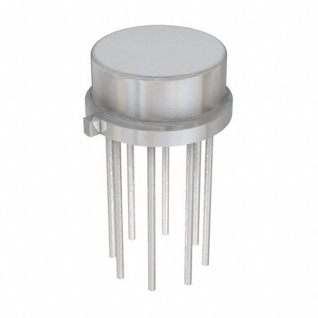
| 描述 | IC OPAMP GP 16MHZ TO99-8高速运算放大器 Prec High-Speed Difet Oper Amp |
| 产品分类 | Linear - Amplifiers - Instrumentation, OP Amps, Buffer Amps集成电路 - IC |
| 品牌 | Texas Instruments |
| 产品手册 | http://www.ti.com/litv/sbos165 |
| 产品图片 |
|
| rohs | 符合RoHS无铅 / 符合限制有害物质指令(RoHS)规范要求 |
| 产品系列 | 放大器 IC,高速运算放大器,Texas Instruments OPA627BMDifet® |
| 数据手册 | |
| 产品型号 | OPA627BM |
| 产品目录页面 | |
| 产品种类 | |
| 供应商器件封装 | TO-99-8 |
| 共模抑制比—最小值 | 106 dB |
| 其它名称 | 296-22025-5 |
| 包装 | 管件 |
| 压摆率 | 55 V/µs |
| 商标 | Texas Instruments |
| 增益带宽生成 | 16 MHz |
| 增益带宽积 | 16MHz |
| 安装类型 | 通孔 |
| 安装风格 | Through Hole |
| 封装 | Tube |
| 封装/外壳 | TO-99-8 金属罐 |
| 封装/箱体 | TO-99-8 |
| 工作温度 | -25°C ~ 85°C |
| 工作电源电压 | 36 V |
| 工厂包装数量 | 1 |
| 拓扑结构 | Voltage Feedback |
| 放大器类型 | 通用 |
| 最大功率耗散 | 1000 mW |
| 最大工作温度 | + 85 C |
| 最小工作温度 | - 25 C |
| 标准包装 | 1 |
| 电压-电源,单/双 (±) | 9 V ~ 36 V, ±4.5 V ~ 18 V |
| 电压-输入失调 | 40µV |
| 电压增益dB | 120 dB |
| 电流-电源 | 7mA |
| 电流-输入偏置 | 1pA |
| 电流-输出/通道 | 45mA |
| 电源电压-最大 | +/- 18 V |
| 电源电压-最小 | +/- 4.5 V |
| 电源电流 | 7.5 mA |
| 电路数 | 1 |
| 系列 | OPA627 |
| 转换速度 | 55 V/us |
| 输入补偿电压 | 0.1 mV |
| 输出类型 | - |
| 通道数量 | 1 Channel |


- 商务部:美国ITC正式对集成电路等产品启动337调查
- 曝三星4nm工艺存在良率问题 高通将骁龙8 Gen1或转产台积电
- 太阳诱电将投资9.5亿元在常州建新厂生产MLCC 预计2023年完工
- 英特尔发布欧洲新工厂建设计划 深化IDM 2.0 战略
- 台积电先进制程称霸业界 有大客户加持明年业绩稳了
- 达到5530亿美元!SIA预计今年全球半导体销售额将创下新高
- 英特尔拟将自动驾驶子公司Mobileye上市 估值或超500亿美元
- 三星加码芯片和SET,合并消费电子和移动部门,撤换高东真等 CEO
- 三星电子宣布重大人事变动 还合并消费电子和移动部门
- 海关总署:前11个月进口集成电路产品价值2.52万亿元 增长14.8%


PDF Datasheet 数据手册内容提取
Product Sample & Technical Tools & Support & Folder Buy Documents Software Community OPA627,OPA637 SBOS165A–SEPTEMBER2000–REVISEDOCTOBER2015 ® OPA627 and OPA637 Precision High-Speed Difet Operational Amplifiers 1 Features The OPA6x7 is fabricated on a high-speed, dielectrically-isolated complementary NPN/PNP • VeryLowNoise:4.5nV/√Hzat10kHz 1 process. It operates over a wide range of power • FastSettlingTime: supply voltage of ±4.5 V to ±18 V. Laser-trimmed – OPA627—550nsto0.01% Difet input circuitry provides high accuracy and low- noise performance comparable with the best bipolar- – OPA637—450nsto0.01% inputoperationalamplifiers. • LowV :100-µVmaximum OS High frequency complementary transistors allow • LowDrift:0.8-µV/°Cmaximum increased circuit bandwidth, attaining dynamic • LowIB:5-pAmaximum performance not possible with previous precision FET • OPA627:Unity-GainStable operational amplifiers. The OPA627 is unity-gain stable. The OPA637 is stable in gains equal to or • OPA637:StableinGain ≥ 5 greaterthanfive. 2 Applications Difet fabrication achieves extremely low input bias currents without compromising input voltage noise • PrecisionInstrumentation performance. Low input bias current is maintained • FastDataAcquisition over a wide input common-mode voltage range with • DACOutputAmplifier uniquecascodecircuitry. • Optoelectronics The OPA6x7 is available in plastic PDIP, SOIC, and • Sonar,Ultrasound metal TO-99 packages. Industrial and military temperaturerangemodelsareavailable. • High-ImpedanceSensorAmps • High-PerformanceAudioCircuitry DeviceInformation(1) • ActiveFilters PARTNUMBER PACKAGE BODYSIZE(NOM) SOIC(8) 3.91mm×4.9mm 3 Description OPA627 PDIP(8) 6.35mm×9.81mm The OPA6x7 Difet® operational amplifiers provide a OPA637 8.95mm(metalcan new level of performance in a precision FET TO-99(8) diameter) operational amplifier. When compared to the popular OPA111 operational amplifier, the OPA6x7 has lower (1) For all available packages, see the orderable addendum at theendofthedatasheet. noise, lower offset voltage, and higher speed. The OPA6x7 is useful in a broad range of precision and highspeedanalogcircuitry. OPA627SimplifiedSchematic 7 Trim Trim +VS 1 5 Output 6 +In –In 3 2 –V S 4 1 An IMPORTANT NOTICE at the end of this data sheet addresses availability, warranty, changes, use in safety-critical applications, intellectualpropertymattersandotherimportantdisclaimers.PRODUCTIONDATA.
OPA627,OPA637 SBOS165A–SEPTEMBER2000–REVISEDOCTOBER2015 www.ti.com Table of Contents 1 Features.................................................................. 1 7.5 DeviceFunctionalModes........................................19 2 Applications........................................................... 1 8 ApplicationandImplementation........................ 20 3 Description............................................................. 1 8.1 ApplicationInformation............................................20 4 RevisionHistory..................................................... 2 8.2 TypicalApplication .................................................22 5 PinConfigurationandFunctions......................... 3 9 PowerSupplyRecommendations...................... 24 6 Specifications......................................................... 3 10 Layout................................................................... 24 6.1 AbsoluteMaximumRatings......................................3 10.1 LayoutGuidelines.................................................24 6.2 ESDRatings ............................................................4 10.2 LayoutExample....................................................25 6.3 RecommendedOperatingConditions.......................4 11 DeviceandDocumentationSupport................. 26 6.4 ThermalInformation..................................................4 11.1 DeviceSupport ....................................................26 6.5 ElectricalCharacteristics...........................................5 11.2 DocumentationSupport .......................................26 6.6 TypicalCharacteristics..............................................7 11.3 RelatedLinks........................................................26 7 DetailedDescription............................................ 12 11.4 Trademarks...........................................................26 7.1 Overview.................................................................12 11.5 ElectrostaticDischargeCaution............................27 7.2 FunctionalBlockDiagram.......................................12 11.6 Glossary................................................................27 7.3 FeatureDescription.................................................12 12 Mechanical,Packaging,andOrderable Information........................................................... 27 7.4 SettlingTime...........................................................19 4 Revision History NOTE:Pagenumbersforpreviousrevisionsmaydifferfrompagenumbersinthecurrentversion. ChangesfromOriginal(September2000)toRevisionA Page • AddedESDRatingstable,FeatureDescriptionsection,DeviceFunctionalModes,ApplicationandImplementation section,PowerSupplyRecommendationssection,Layoutsection,DeviceandDocumentationSupportsection,and Mechanical,Packaging,andOrderableInformationsection. ................................................................................................ 1 • RemovedLeadTemperaturefromAbsoluteMaximumRatingstable. ................................................................................. 3 2 SubmitDocumentationFeedback Copyright©2000–2015,TexasInstrumentsIncorporated ProductFolderLinks:OPA627 OPA637
OPA627,OPA637 www.ti.com SBOS165A–SEPTEMBER2000–REVISEDOCTOBER2015 5 Pin Configuration and Functions PandDPackages 8-PinPDIPandSOIC LMCPackage TopView 8-PinTO-99 TopView No Internal Connection OffsetTrim 1 8 No Internal Connection –In 2 7 +V 8 +V S OffsetTrim S 1 7 +In 3 6 Output –VS 4 5 OffsetTrim –In 2 6 Output 3 5 +In 4 OffsetTrim –V S Case connected to–V . S PinFunctions PIN I/O DESCRIPTION NO. NAME 1 OffsetTrim — Inputoffsetvoltagetrim(leavefloatingifnotused) 2 –In I Invertinginput 3 +In I Noninvertinginput 4 –V — Negative(lowest)powersupply S 5 OffsetTrim — Inputoffsetvoltagetrim(leavefloatingifnotused) 6 Output O Output 7 +V — Positive(highest)powersupply S 8 NC — Nointernalconnection(canbeleftfloating) 6 Specifications 6.1 Absolute Maximum Ratings overoperatingfree-airtemperaturerange(unlessotherwisenoted) (1) MIN MAX UNIT SupplyVoltage ±18 V InputVoltageRange +V +2 –V –2 V S S DifferentialInput TotalV +4 V S PowerDissipation 1000 mW LMCPackage –55 125 OperatingTemperature °C P,DPackage –40 125 LMCPackage 175 JunctionTemperature °C P,DPackage 150 LMCPackage –65 150 Storagetemperature,T °C stg P,DPackage –40 125 (1) StressesbeyondthoselistedunderAbsoluteMaximumRatingsmaycausepermanentdamagetothedevice.Thesearestressratings only,whichdonotimplyfunctionaloperationofthedeviceattheseoranyotherconditionsbeyondthoseindicatedunderRecommended OperatingConditions.Exposuretoabsolute-maximum-ratedconditionsforextendedperiodsmayaffectdevicereliability. Copyright©2000–2015,TexasInstrumentsIncorporated SubmitDocumentationFeedback 3 ProductFolderLinks:OPA627 OPA637
OPA627,OPA637 SBOS165A–SEPTEMBER2000–REVISEDOCTOBER2015 www.ti.com 6.2 ESD Ratings VALUE UNIT OPA627andOPA637inPDIPandSOICPackages V Electrostatic Human-bodymodel(HBM),perANSI/ESDA/JEDECJS-001(1) ±2500 V (ESD) discharge OPA627andOPA637inSOICPackages V Electrostatic Charged-devicemodel(CDM),perJEDECspecificationJESD22-C101(2) ±1000 V (ESD) discharge (1) JEDECdocumentJEP155statesthat500-VHBMallowssafemanufacturingwithastandardESDcontrolprocess. (2) JEDECdocumentJEP157statesthat250-VCDMallowssafemanufacturingwithastandardESDcontrolprocess. 6.3 Recommended Operating Conditions overoperatingfree-airtemperaturerange(unlessotherwisenoted) MIN NOM MAX UNIT Supplyvoltage,Vs=(V+)-(V-) 9(±4.5) 30(±15) 36(±18) V Specified PandDpackages –25 25 85 °C temperature LMCpackage –55 25 125 °C 6.4 Thermal Information OPA627,OPA637 THERMALMETRIC(1) P(DIP) D(SOIC) LMC(TO-99) UNIT 8PINS 8PINS 8PINS R Junction-to-ambientthermalresistance 46.2 107.9 200 °C/W θJA R Junction-to-case(top)thermalresistance 34.5 57.3 — °C/W θJC(top) R Junction-to-boardthermalresistance 23.5 49.7 — °C/W θJB ψ Junction-to-topcharacterizationparameter 11.7 11.7 — °C/W JT ψ Junction-to-boardcharacterizationparameter 23.3 48.9 — °C/W JB R Junction-to-case(bottom)thermalresistance N/A N/A — °C/W θJC(bot) (1) Formoreinformationabouttraditionalandnewthermalmetrics,seetheSemiconductorandICPackageThermalMetricsapplication report,SPRA953. 4 SubmitDocumentationFeedback Copyright©2000–2015,TexasInstrumentsIncorporated ProductFolderLinks:OPA627 OPA637
OPA627,OPA637 www.ti.com SBOS165A–SEPTEMBER2000–REVISEDOCTOBER2015 6.5 Electrical Characteristics AtT =25°C,andV =±15V,unlessotherwisenoted. A S PARAMETER TESTCONDITIONS MIN TYP MAX UNIT OFFSETVOLTAGE(1) BM,SMgrades 40 100 AMgrade 130 250 Inputoffsetvoltage µV BPgrade 100 250 AP,AUgrades 280 500 BM,SMgrades 0.4 0.8 AMgrade 1.2 2 Averagedrift µV/°C BPgrade 0.8 2 AP,AUgrades 2.5 BM,BP,SMgrades 106 120 Powersupplyrejection VS=±4.5to±18V dB AM,AP,AUgrades 100 116 INPUTBIASCURRENT(2) BM,BP,SMgrades 1 5 TA=25°C pA AM,AP,AUgrades 2 10 VCM=0V BM,BPgrades 1 Overspecified Inputbiascurrent SMgrade 50 nA temperature AM,AP,AUgrades 2 BM,BP,SMgrades 1 VCM=±10V,overcommon-modevoltage pA AM,AP,AUgrades 2 BM,BP,SMgrades 0.5 5 TA=25°C pA AM,AP,AUgrades 1 10 Inputoffsetcurrent VCM=0V BM,BPgrades 1 Overspecified SMgrade 50 nA temperature AM,AP,AUgrades 2 NOISE BM,BP,SMgrades 15 40 f=10Hz AM,AP,AUgrades 20 BM,BP,SMgrades 8 20 f=100Hz AM,AP,AUgrades 10 Inputvoltagenoisedensity nV/√Hz BM,BP,SMgrades 5.2 8 f=1kHz AM,AP,AUgrades 5.6 BM,BP,SMgrades 4.5 6 f=10kHz AM,AP,AUgrades 4.8 BM,BP,SMgrades 0.6 1.6 Inputvoltagenoise BW=0.1Hzto10Hz µVp-p AM,AP,AUgrades 0.8 Inputbias-currentnoise BM,BP,SMgrades 1.6 2.5 f=100Hz fA/√Hz density AM,AP,AUgrades 2.5 BM,BP,SMgrades 30 60 Inputbias-currentnoise BW=0.1Hzto10Hz fAp-p AM,AP,AUgrades 48 INPUTIMPEDANCE Differential 1013||8 Ω||pF Common-mode 1013||7 Ω||pF INPUTVOLTAGERANGE TA=25°C ±11 ±11.5 Common-modeinputrange V Overspecifiedtemperature ±10.5 ±11 BM,BP,SMgrades 106 116 Common-moderejection VCM=±10.5V dB AM,AP,AUgrades 100 110 (1) Offsetvoltagemeasuredfullywarmed-up. (2) High-speedtestatT =25°C.SeeTypicalCharacteristicsforwarmed-upperformance. J Copyright©2000–2015,TexasInstrumentsIncorporated SubmitDocumentationFeedback 5 ProductFolderLinks:OPA627 OPA637
OPA627,OPA637 SBOS165A–SEPTEMBER2000–REVISEDOCTOBER2015 www.ti.com Electrical Characteristics (continued) AtT =25°C,andV =±15V,unlessotherwisenoted. A S PARAMETER TESTCONDITIONS MIN TYP MAX UNIT OPEN-LOOPGAIN BM,BP,SMgrades 112 120 TA=25°C AM,AP,AUgrades 106 116 Open-loopvoltagegain VO=±10V,RL=1kΩ BM,BPgrades 106 117 dB Overspecified SMgrade 100 114 temperature AM,AP,AUgrades 100 110 FREQUENCYRESPONSE G=–1,10-Vstep,OPA627 40 55 Slewrate V/µs G=–4,10-Vstep,OPA637 100 135 G=–1,10-Vstep, 0.01% 550 OPA627 0.1% 450 Settlingtime ns G=–4,10-Vstep, 0.01% 450 OPA637 0.1% 300 G=1,OPA627 16 Gain-bandwidthproduct MHz G=10,OPA637 80 Totalharmonicdistortion+ G=1,f=1kHz 0.00003% noise POWERSUPPLY Specifiedoperatingvoltage ±15 V Operatingvoltagerange ±4.5 ±18 V Current ±7 ±7.5 mA OUTPUT RL=1kΩ ±11.5 ±12.3 Voltageoutput V Overspecifiedtemperature ±11 ±11.5 Currentoutput VO=±10V ±45 mA Short-circuitcurrent ±35 ±70/–55 ±100 mA Outputimpedance,open-loop 1MHz 55 Ω TEMPERATURERANGE Temperaturerange AP,BP,AM,BM,AUgrades –25 85 °C specification SMgrade –55 125 6 SubmitDocumentationFeedback Copyright©2000–2015,TexasInstrumentsIncorporated ProductFolderLinks:OPA627 OPA637
OPA627,OPA637 www.ti.com SBOS165A–SEPTEMBER2000–REVISEDOCTOBER2015 6.6 Typical Characteristics AtT =25°C,andV =±15V,unlessotherwisenoted. A S 1k 100 p-p Noise Bandwidth: √oise (nV/ Hz) 100 ge Noise (µV) 101 0fr.e1qHuze ntoc yin.dicated N a e olt Voltag 10 nput V 0.1 I RMS 1 0.01 1 10 100 1k 10k 100k 1M 10M 1 10 100 1k 10k 100k 1M 10M Frequency (Hz) Bandwidth (Hz) Figure1.InputVoltageNoiseSpectralDensityvsFrequency Figure2.TotalInputVoltageNoisevsBandwidth 1k 140 – 120 √nV/ Hz) 100 RS+ n (dB) 10800 OPA637 oise ( Comparison with e Gai 60 N OPA627 + Resistor g age 10 OAPmA2p7 + B Ripeoslaisrt oOrp Volta 40 OPA627 olt 20 V Spot Noise Resistor Noise Only at 10kHz 0 1 –20 100 1k 10k 100k 1M 10M 100M 1 10 100 1k 10k 100k 1M 10M 100M Source Resistance ( Ω ) Frequency (Hz) Figure3.VoltageNoisevsSourceResistance Figure4.Open-LoopGainvsFrequency 30 –90 30 –90 Gain (dB) 2100 Gain 75M° aPrhgainse Phase ––112500 Phase (Degrees) Gain (dB) 2100 Gain Phase ––112500 Phase (Degrees) 0 –180 0 –180 –10 –210 –10 –210 1 10 100 1 10 100 Frequency (MHz) Frequency (MHz) Figure5.OPA627Gain/PhasevsFrequency Figure6.OPA637Gain/PhasevsFrequency Copyright©2000–2015,TexasInstrumentsIncorporated SubmitDocumentationFeedback 7 ProductFolderLinks:OPA627 OPA637
OPA627,OPA637 SBOS165A–SEPTEMBER2000–REVISEDOCTOBER2015 www.ti.com Typical Characteristics (continued) AtT =25°C,andV =±15V,unlessotherwisenoted. A S 125 100 120 )Ω 80 Gain (dB) 115 esistance ( 60 Voltage 110 Output R 40 20 105 0 –75 –50 –25 0 25 50 75 100 125 2 20 200 2k 20k 200k 2M 20M Temperature (°C) Frequency (Hz) Figure7.Open-LoopGainvsTemperature Figure8.Open-LoopOutputImpedancevsFrequency 140 130 B) Ratio (d 112000 OPA637 on (dB) 120 ection 80 OPA627 Rejecti 110 Rej de de 60 Mo 100 n-Mo 40 mon- mmo 20 Com 90 o C 0 80 1 10 100 1k 10k 100k 1M 10M –15 –10 –5 0 5 10 15 Frequency (Hz) Common-Mode Voltage (V) Figure9.Common-ModeRejectionvsFrequency Figure10.Common-ModeRejectionvsInputCommon-Mode Voltage 140 125 B) 120 PSR d ection ( 100 –VSPSRR 627 R (dB) 120 y Rej 80 and 637 d PS 115 CMR uppl 60 R an wer-S 40 +VSPSRR 663277 CM 110 o P 20 0 105 1 10 100 1k 10k 100k 1M 10M –75 –50 –25 0 25 50 75 100 125 Frequency (Hz) Temperature (°C) Figure11.Power-SupplyRejectionvsFrequency Figure12.Power-SupplyRejectionandCommon-Mode RejectionvsTemperature 8 SubmitDocumentationFeedback Copyright©2000–2015,TexasInstrumentsIncorporated ProductFolderLinks:OPA627 OPA637
OPA627,OPA637 www.ti.com SBOS165A–SEPTEMBER2000–REVISEDOCTOBER2015 Typical Characteristics (continued) AtT =25°C,andV =±15V,unlessotherwisenoted. A S 8 100 +I at V = 0V 80 L O ply Current (mA) 7.57 ut Current (mA) 6400 +ILat VO= +10V p p Su 6.5 Out –ILat VO= 0V 20 –I at V =–10V L O 6 0 –75 –50 –25 0 25 50 75 100 125 –75 –50 –25 0 25 50 75 100 125 Temperature (°C) Temperature (°C) Figure13.SupplyCurrentvsTemperature Figure14.OutputCurrentLimitvsTemperature 24 60 120 160 Slew Rate z) 20 Hz) 100 140 Gain-Bandwidth (MH 1162 GBWSlew Rate 55 Slew Rate (V/µs) Gain-Bandwidth (M 8600 GBW 112000 Slew Rate (V/µs) 8 50 40 80 –75 –50 –25 0 25 50 75 100 125 –75 –50 –25 0 25 50 75 100 125 Temperature (°C) Temperature (°C) Figure15.OPA627Gain-BandwidthandSlewRatevs Figure16.OPA637Gain-BandwidthandSlewRatevs Temperature Temperature 0.1 1 VI G = +1 + VO = ±10V VIG = +10+ VO = ±10V VIG = +10 + VO = ±10V VIG = +50 + VO = ±10V 0.01 – 600Ω 100pF – 5kΩ 600Ω 100pF 0.1 – 5kΩ 600Ω 100pF – 5kΩ 600Ω 100pF 549Ω +N (%) 0.001 Measurement BW: 80kHz N (%) 0.01 549Ω 102Ω HD D+ G = +50 T G = +10 TH Measurement BW: 80kHz 0.0001 0.001 G = +1 G = +10 0.00001 0.0001 20 100 1k 10k 20k 20 100 1k 10k 20k Frequency (Hz) Frequency (Hz) Figure17.OPA627TotalHarmonicDistortion+Noisevs Figure18.OPA637TotalHarmonicDistortion+Noisevs Frequency Frequency Copyright©2000–2015,TexasInstrumentsIncorporated SubmitDocumentationFeedback 9 ProductFolderLinks:OPA627 OPA637
OPA627,OPA637 SBOS165A–SEPTEMBER2000–REVISEDOCTOBER2015 www.ti.com Typical Characteristics (continued) AtT =25°C,andV =±15V,unlessotherwisenoted. A S 10k 20 NOTE: Measured fully Current (pA) 1010k IB as Current (pA) 1150 warmed-up. TOP-9la9stic Input 10 IOS Input Bi 5 DIP, SOIC 1 TO-99 with 0807HS Heat Sink 0.1 0 –50 –25 0 25 50 75 100 125 150 ±4 ±6 ±8 ±10 ±12 ±14 ±16 ±18 JunctionTemperature (°C) Supply Voltage (±VS) Figure19.InputBiasandOffsetCurrentvsJunction Figure20.InputBiasCurrentvsPowerSupplyVoltage Temperature 1.2 50 Beyond Linear ultiplier 1.1 Common-Mode Range ge (µV) 25 M n ent Cha urr 1 ge 0 C a nput Bias 0.9 Beyond Linear Offset Volt –25 I Common-Mode Range 0.8 –50 –15 –10 –5 0 5 10 15 0 1 2 3 4 5 6 Common-Mode Voltage (V) Time From PowerTurn-On (Min) Figure21.InputBiasCurrentvsCommon-ModeVoltage Figure22.InputOffsetVoltageWarm-upvsTime 30 100 ge (Vp-p) 20 e (µs) 10 Error Band: ±0.01% Output Volta 10 OPA637 SettlingTim 1 OPA627 OPA637 OPA627 0 0.1 100k 1M 10M 100M –1 –10 –100 –1000 Frequency (Hz) Closed-Loop Gain (V/V) Figure23.MaximumOutputVoltagevsFrequency Figure24.SettlingTimevsClosed-LoopGain 10 SubmitDocumentationFeedback Copyright©2000–2015,TexasInstrumentsIncorporated ProductFolderLinks:OPA627 OPA637
OPA627,OPA637 www.ti.com SBOS165A–SEPTEMBER2000–REVISEDOCTOBER2015 Typical Characteristics (continued) AtT =25°C,andV =±15V,unlessotherwisenoted. A S 1500 3 C F R +5V OPA627 OPA637 me (ns) 1000 I –+ R2FkΩ –5V RRCIFF262kpkΩΩF 5420pk0FΩΩ me (µs) 2 E±0rr.o0r1 %Band: OGP =A–6437 Ti Ti Settling 500 OGP =A–6127 Settling 1 OGP =A–6127 OPA637 G =–4 0 0 0.001 0.01 0.1 1 10 0 150 200 300 400 500 Error Band (%) Load Capacitance (pF) Figure25.SettlingTimevsErrorBand Figure26.SettlingTimevsLoadCapacitance Copyright©2000–2015,TexasInstrumentsIncorporated SubmitDocumentationFeedback 11 ProductFolderLinks:OPA627 OPA637
OPA627,OPA637 SBOS165A–SEPTEMBER2000–REVISEDOCTOBER2015 www.ti.com 7 Detailed Description 7.1 Overview The OPA6x7 Difet operational amplifiers provide a new level of performance in a precision FET operational amplifier. When compared to the popular OPA111 operational amplifier, the OPA6x7 has lower noise, lower offset voltage, and higher speed. The OPA6x7 is useful in a broad range of precision and high speed analog circuitry. The OPA6x7 is fabricated on a high-speed, dielectrically-isolated complementary NPN/PNP process. It operates over a wide range of power supply voltage of ±4.5 V to ±18 V. Laser-trimmed Difet input circuitry provides high accuracyandlow-noiseperformancecomparablewiththebestbipolar-inputoperationalamplifiers. High frequency complementary transistors allow increased circuit bandwidth, attaining dynamic performance not possible with previous precision FET operational amplifiers. The OPA627 is unity-gain stable. The OPA637 is stableingainsequaltoorgreaterthanfive. Difet fabrication achieves extremely low input bias currents without compromising input voltage noise performance. Low input bias current is maintained over a wide input common-mode voltage range with unique cascodecircuitry. The OPA6x7 is available in plastic PDIP, SOIC, and metal TO-99 packages. Industrial and military temperature rangemodelsareavailable. 7.2 Functional Block Diagram 7 Trim Trim +VS 1 5 Output 6 +In –In 3 2 –V S 4 7.3 Feature Description The OPA627 is unity-gain stable. The OPA637 may achieve higher speed and bandwidth in circuits with noise gain greater than five. Noise gain refers to the closed-loop gain of a circuit, as if the noninverting operational amplifier input were being driven. For example, the OPA637 may be used in a noninverting amplifier with gain greaterthanfive,oraninvertingamplifierofgaingreaterthanfour. When choosing between the OPA627 or OPA637, consider the high frequency noise gain of your circuit configuration. Circuits with a feedback capacitor (see Figure 27) place the operational amplifier in unity noise- gainathighfrequency.TheseapplicationsmustusetheOPA627forproperstability.Anexceptionisthecircuitin Figure 28, where a small feedback capacitance is used to compensate for the input capacitance at the inverting input of the operational amplifier. In this case, the closed-loop noise gain remains constant with frequency, so if theclosed-loopgainisequaltofiveorgreater,theOPA637maybeused. 12 SubmitDocumentationFeedback Copyright©2000–2015,TexasInstrumentsIncorporated ProductFolderLinks:OPA627 OPA637
OPA627,OPA637 www.ti.com SBOS165A–SEPTEMBER2000–REVISEDOCTOBER2015 Feature Description (continued) R < 4R F I OPA627 OPA627 – – + + Buffer Non-InvertingAmp RI G < 5 R < 4R F OPA627 RI OPA627 – – + + Bandwidth InvertingAmp Limiting G < |–4| OPA627 OPA627 – – + + Integrator Filter Figure27. CircuitsWithNoiseGainLessThanFiveRequiretheOPA627forProperStability C 2 C R 1 2 – + OPA637 R1 C1= CIN+ CSTRAY R C C = 1 1 2 R 2 Figure28. CircuitsWithNoiseGainEqualtoorGreaterThanFiveMayUsetheOPA637 7.3.1 OffsetVoltageAdjustment The OPA6x7 is laser-trimmed for low offset voltage and drift, so many circuits will not require external adjustment. Figure 29 shows the optional connection of an external potentiometer to adjust offset voltage. This adjustment should not be used to compensate for offsets created elsewhere in a system (such as in later amplification stages or in an A/D converter), because this could introduce excessive temperature drift. Generally, the offset drift will change by approximately 4 µV/°C for 1 mV of change in the offset voltage due to an offset adjustment(asshowninFigure29). Copyright©2000–2015,TexasInstrumentsIncorporated SubmitDocumentationFeedback 13 ProductFolderLinks:OPA627 OPA637
OPA627,OPA637 SBOS165A–SEPTEMBER2000–REVISEDOCTOBER2015 www.ti.com Feature Description (continued) +V S 100kΩ 7 10kΩto 1MΩ 1 Potentiometer 2 – 5 (100kΩpreferred) 3 6 + OPA627/637 4 ±10mVTypical Trim Range –V S Figure29. OptionalOffsetVoltageTrimCircuit 7.3.2 NoisePerformance Some bipolar operational amplifiers may provide lower voltage noise performance, but both voltage noise and biascurrentnoisecontributetothetotalnoiseofasystem.TheOPA6x7providesbothlowvoltagenoiseandlow current noise. This provides optimum noise performance over a wide range of sources, including reactive-source impedances. This can be seen in the performance curve showing the noise of a source resistor combined with the noise of an OPA627. Above a 2-kΩ source resistance, the operational amplifier contributes little additional noise. Below 1 kΩ, operational amplifier noise dominates over the resistor noise, but compares favorably with precisionbipolaroperationalamplifiers. 7.3.3 InputBiasCurrent Difet fabrication of the OPA6x7 provides low input bias current. Because the gate current of a FET doubles approximatelyevery10°C,toachievelowestinputbiascurrent,keepthedietemperatureaslowaspossible.The highspeed,andthereforehigherquiescentcurrent,oftheOPA6x7canleadtohigherchiptemperature.Asimple press-on heat sink such as the Burr-Brown model 807HS (TO-99 metal package) can reduce chip temperature by approximately 15°C, lowering the I to one-third its warmed-up value. The 807HS heat sink can also reduce B low-frequency voltage noise caused by air currents and thermoelectric effects. See the data sheet on the 807HS fordetails. Temperature rise in the plastic PDIP and SOIC packages can be minimized by soldering the device to the circuit board.Widecoppertracesalsohelpdissipateheat. The OPA6x7 may also be operated at reduced power supply voltage, to minimize power dissipation and temperature rise. Using ±5-V power supplies reduces power dissipation to one-third of that at ±15 V. This reducestheI ofTO-99metalpackagedevicestoapproximatelyone-fourththevalueat ±15V. B Leakage currents between printed-circuit-board traces can easily exceed the input bias current of the OPA6x7. A circuit board guard pattern (see Figure 30) reduces leakage effects. By surrounding critical high impedance input circuitry with a low impedance circuit connection at the same potential, leakage current will flow harmlessly to the low-impedancenode.Thecase(TO-99metalpackageonly)isinternallyconnectedto –V . S Input bias current may also be degraded by improper handling or cleaning. Contamination from handling parts andcircuitboardsmayberemovedwithcleaningsolventsanddeionizedwater.Eachrinsingoperationshouldbe followedbya30-minutebakeat85°C. Many FET-input operational amplifiers exhibit large changes in input bias current with changes in input voltage. Input stage cascode circuitry makes the input bias current of the OPA6x7 virtually constant with wide common- modevoltagechanges.Thisisidealforaccurate,highinput-impedancebufferapplications. 14 SubmitDocumentationFeedback Copyright©2000–2015,TexasInstrumentsIncorporated ProductFolderLinks:OPA627 OPA637
OPA627,OPA637 www.ti.com SBOS165A–SEPTEMBER2000–REVISEDOCTOBER2015 Feature Description (continued) Non-inverting Buffer 2 2 – – 6 6 Out Out In 3 + In 3 + OPA627 OPA627 TO-99 Bottom View Inverting In 2 OPA627 3 4 – 5 6 Out 3 + 2 6 BoardLayoutforInputGuarding: Guardtopandbottomofboard. 7 Alternate—useTeflon®standoffforsen- 1 sitiveinputpins. 8 No Internal Connection Teflon®E.I.duPontdeNemours&Co. To Guard Drive . B Figure30. ConnectionofInputGuardforLowestI B 7.3.4 Phase-ReversalProtection The OPA6x7 has internal phase-reversal protection. Many FET-input operational amplifiers exhibit a phase reversal when the input is driven beyond its linear common-mode range. This is most often encountered in noninvertingcircuitswhentheinputisdrivenbelow –12V,causingtheoutputtoreverseintothepositiverail.The input circuitry of the OPA6x7 does not induce phase reversal with excessive common-mode voltage, so the outputlimitsintotheappropriaterail. 7.3.5 OutputOverload When the inputs to the OPA6x7 are overdriven, the output voltage of the OPA6x7 smoothly limits at approximately 2.5 V from the positive and negative power supplies. If driven to the negative swing limit, recovery takes approximately 500 ns. When the output is driven into the positive limit, recovery takes approximately 6 µs. Output recovery of the OPA627 can be improved using the output clamp circuit shown in Figure 31. Placing diodesattheinvertinginputpreventdegradationofinputbiascurrent. +V S 5kΩ (2) HP5082-2811 ZD Diode Bridge 1 BB: PWS740-3 1kΩ 5kΩ ZD1 : 10V IN961 R F VI – –VS RI VO + OPA627 Clamps output at V = ±11.5V O Figure31. ClampCircuitforImprovedOverloadRecovery Copyright©2000–2015,TexasInstrumentsIncorporated SubmitDocumentationFeedback 15 ProductFolderLinks:OPA627 OPA637
OPA627,OPA637 SBOS165A–SEPTEMBER2000–REVISEDOCTOBER2015 www.ti.com Feature Description (continued) 7.3.6 CapacitiveLoads As with any high-speed operational amplifier, best dynamic performance can be achieved by minimizing the capacitive load. Because a load capacitance presents a decreasing impedance at higher frequency, a load capacitancewhichiseasilydrivenbyaslowoperationalamplifiercancauseahigh-speedoperationalamplifierto perform poorly. See the typical curves showing settling times as a function of capacitive load. The lower bandwidth of the OPA627 makes it the better choice for driving large capacitive loads. Figure 32 shows a circuit for driving very large load capacitance. The two-pole response of this circuit can also be used to sharply limit system bandwidth, often useful in reducing the noise of systems which do not require the full bandwidth of the OPA627. R F 1kΩ 200pF C G = +1 F RO BW ≥ 1MHz – 20Ω + C R OPA627 5nLF G = 1+RF R1 1 Optional Gain ForApproximate Butterworth Response: Gain > 1 CF=2 RROCL RF>> RO F 1 f = –3dB 2p√R R C C F O F L Figure32. DrivingLargeCapacitiveLoads 7.3.7 InputProtection TheinputsoftheOPA6x7areprotectedforvoltagesfrom+V +2Vto –V – 2V.Iftheinputvoltagecanexceed S S these limits, the amplifier should be protected. The diode clamps shown in (a) in Figure 33 prevent the input voltage from exceeding one forward diode voltage drop beyond the power supplies, which is well within the safe limits. If the input source can deliver current in excess of the maximum forward current of the protection diodes, useaseriesresistor,R ,tolimitthecurrent.Beawarethataddingresistancetotheinputincreasesnoise.The4- S nV/√Hz theoretical thermal noise of a 1-kΩ resistor will add to the 4.5-nV/√Hz noise of the OPA6x7 (by the square-root of the sum of the squares), producing a total noise of 6 nV/√Hz. Resistors less than 100 Ω add negligiblenoise. Leakage current in the protection diodes can increase the total input bias current of the circuit. The specified maximum leakage current for commonly used diodes such as the 1N4148 is approximately 25 nA, more than a thousand times larger than the input bias current of the OPA6x7. Leakage current of these diodes is typically much lower and may be adequate in many applications. Light falling on the junction of the protection diodes can dramatically increase leakage current, so common glass-packaged diodes should be shielded from ambient light. Very low leakage can be achieved by using a diode-connected FET as shown. The 2N4117A is specified at 1 pA anditsmetalcaseshieldsthejunctionfromlight. Sometimes input protection is required on I/V converters of inverting amplifiers; see (b) in Figure 33. Although in normal operation, the voltage at the summing junction will be near zero (equal to the offset voltage of the amplifier),andlargeinputtransientsmaycausethisnodetoexceed2Vbeyondthepowersupplies.Inthiscase, the summing junction should be protected with diode clamps connected to ground. Even with the low voltage present at the summing junction, common signal diodes may have excessive leakage current. Because the reverse voltage on these diodes is clamped, a diode-connected signal transistor can act as an inexpensive low leakagediode;see(b)inFigure33. 16 SubmitDocumentationFeedback Copyright©2000–2015,TexasInstrumentsIncorporated ProductFolderLinks:OPA627 OPA637
OPA627,OPA637 www.ti.com SBOS165A–SEPTEMBER2000–REVISEDOCTOBER2015 Feature Description (continued) +V S – D VO + OPA627 D D: IN4148—25nALeakage Optional R S 2N4117A—1pALeakage –V Siliconix S = (a) I IN – V O D D + OPA627 D: 2N3904 = (b) NC Figure33. InputProtectionCircuits 7.3.8 EMIRejectionRatio(EMIRR) The electromagnetic interference (EMI) rejection ratio, or EMIRR, describes the EMI immunity of operational amplifiers.Anadverseeffectthatiscommontomanyoperationalamplifiersisachangeintheoffsetvoltageasa result of RF signal rectification. An operational amplifier that is more efficient at rejecting this change in offset as a result of EMI has a higher EMIRR and is quantified by a decibel value. Measuring EMIRR can be performed in many ways, but this report provides the EMIRR IN+, which specifically describes the EMIRR performance when the RF signal is applied to the noninverting input pin of the operational amplifier. In general, only the noninverting inputistestedforEMIRRforthefollowingthreereasons: • Operational amplifier input pins are known to be the most sensitive to EMI, and typically rectify RF signals betterthanthesupplyoroutputpins. • The noninverting and inverting operational amplifier inputs have symmetrical physical layouts and exhibit nearlymatchingEMIRRperformance. • EMIRR is easier to measure on noninverting pins than on other pins because the noninverting input terminal can be isolated on a printed-circuit-board (PCB). This isolation allows the RF signal to be applied directly to the noninverting input terminal with no complex interactions from other components or connecting PCB traces. A more formal discussion of the EMIRR IN+ definition and test method is provided in application report EMI RejectionRatioofOperationalAmplifiers (SBOA128),availablefordownloadatwww.ti.com. The EMIRR IN+ of the OPA627 is plotted versus frequency as shown in Figure 34. If available, any dual and quad operational amplifier device versions have nearly similar EMIRR IN+ performance. The OPA627 unity-gain bandwidth is 16 MHz. EMIRR performance below this frequency denotes interfering signals that fall within the operationalamplifierbandwidth. Copyright©2000–2015,TexasInstrumentsIncorporated SubmitDocumentationFeedback 17 ProductFolderLinks:OPA627 OPA637
OPA627,OPA637 SBOS165A–SEPTEMBER2000–REVISEDOCTOBER2015 www.ti.com Feature Description (continued) 140 PRF = -10 dbm 120 VS = r15 V VCM = 0 V 100 b) d + ( 80 N R I R 60 MI E 40 20 0 10M 100M 1G 10G Frequency (MHz) Figure34. OPA627EMIRRIN+vsFrequency Table 1 shows the EMIRR IN+ values for the OPA627 at particular frequencies commonly encountered in real- world applications. Applications listed in Table 1 may be centered on or operated near the particular frequency shown. This information may be of special interest to designers working with these types of applications, or working in other fields likely to encounter RF interference from broad sources, such as the industrial, scientific, andmedical(ISM)radioband. Table1.OPA627EMIRRIN+forFrequenciesofInterest FREQUENCY APPLICATION/ALLOCATION EMIRRIN+ 400MHz Mobileradio,mobilesatellite/spaceoperation,weather,radar,UHF 46.2dB GSM,radiocom/nav./GPS(to1.6GHz),ISM,aeronauticalmobile, 900MHz 60.3dB UHF 1.8GHz GSM,mobilepersonalcomm.broadband,satellite,L-band 81dB 802.11b/g/n,Bluetooth™,mobilepersonalcomm.,ISM,amateur 2.4GHz 96.9dB radio/satellite,S-band 3.6GHz Radiolocation,aerocomm./nav.,satellite,mobile,S-band 108.9dB 802.11a/n,aerocomm./nav.,mobilecomm.,space/satellite 5Ghz 116.8dB operation,C-band 7.3.8.1 EMIRRIN+TestConfiguration Figure 35 shows the circuit configuration for testing the EMIRR IN+. An RF source is connected to the operational amplifier noninverting input terminal using a transmission line. The operational amplifier is configured in a unity gain buffer topology with the output connected to a low-pass filter (LPF) and a digital multimeter (DMM). A large impedance mismatch at the operational amplifier input causes a voltage reflection; however, this effect is characterized and accounted for when determining the EMIRR IN+. The resulting DC offset voltage is sampled and measured by the multimeter. The LPF isolates the multimeter from residual RF signals that may interferewithmultimeteraccuracy.RefertoSBOA128 formoredetails. 18 SubmitDocumentationFeedback Copyright©2000–2015,TexasInstrumentsIncorporated ProductFolderLinks:OPA627 OPA637
OPA627,OPA637 www.ti.com SBOS165A–SEPTEMBER2000–REVISEDOCTOBER2015 Ambient temperature: 25(cid:219)& +VS – 50 (cid:13)(cid:3) Low-Pass Filter + RF source DC Bias: 0 V -VS Sample / Modulation: None (CW) Digital Multimeter Frequency Sweep: 201 pt. Log Not shown: 0.1 µF and 10 µF Averaging supply decoupling Figure35. EMIRRIN+TestConfigurationSchematic 7.4 Settling Time The OPA627 and OPA637 have fast settling times, as low as 300 ns. Figure 36 illustrates the circuit used to measuresettlingtimefortheOPA627andOPA637. Error Out RI/ 2kWΩ OPA627 OPA637 C F R,R 2kΩ 500Ω I 1 HP- C 6pF 4pF F 5082- 2kΩ ErrorBand ±0.5mV ±0.2mV 2835 (0.01%) +15V R High Quality I – Pulse Generator ±5V NOTE:CFisselectedforbestsettlingtimeperformance dependingontestfixturelayout.Onceoptimumvalueis 51Ω + Out determined,afixedcapacitormaybeused. –15V Figure36. SettlingTimeandSlewRateTestCircuit 7.5 Device Functional Modes The OPA627 and OPA6377 have a single functional mode and are operational when the power-supply voltage is greaterthan9V(±4.5V).ThemaximumpowersupplyvoltagefortheOPA627andOPA637are36V(±18V). Copyright©2000–2015,TexasInstrumentsIncorporated SubmitDocumentationFeedback 19 ProductFolderLinks:OPA627 OPA637
OPA627,OPA637 SBOS165A–SEPTEMBER2000–REVISEDOCTOBER2015 www.ti.com 8 Application and Implementation NOTE Information in the following applications sections is not part of the TI component specification, and TI does not warrant its accuracy or completeness. TI’s customers are responsible for determining suitability of components for their purposes. Customers should validateandtesttheirdesignimplementationtoconfirmsystemfunctionality. 8.1 Application Information The OPA627 and OPA637 are ideally suited to use as input amplifiers in instrumentation amplifier configurations requiringhighspeed,fastsettlingandhighinputimpedance. Gain = 100 OPA637 CMRR » 116dB –In + Bandwidth » 1MHz – RF 5kWΩ 2 25kΩ 25kΩ 5 Input Common-Mode Range = ±5V INA105 R 101GΩ 3pF DAifmfeprelinfietiarl – 6 Output 3 + RF 25kΩ – 5kΩ 25kΩ +In + 1 OPA637 Differential Voltage Gain = 1 + 2R /R F G Figure37. HighSpeedInstrumentationAmplifier,Gain=100 Gain = 1000 OPA637 CMRR » 116dB –In + Bandwidth » 400kHz – RF 5kΩ 2 10kΩ 100kΩ 5 Input Common-Mode Range = ±10V INA106 R 101GΩ 3pF DAifmfeprelinfietiarl – 6 Output 3 + RF 10kΩ – 5kΩ 100kΩ +In + 1 OPA637 Differential Voltage Gain = (1 + 2R /R )•10 F G Figure38. HighSpeedInstrumentationAmplifier,Gain=1000 ThiscompositeamplifierusestheOPA603current-feedbackopampto R2 provideextendedbandwidthandslewrateathighclosed-loopgain.The feedback loop is closed around the composite amp, preserving the precisioninputcharacteristicsoftheOPA627/637.Useseparatepower – supplybypasscapacitorsforeachopamp. A1 + ∗Minimizecapacitanceatthisnode. V + V I O – R OPA603 foRr L±‡101V5 0OΩut G(VA/VIN) OPAA1MWP (RΩ1) (kRΩ2) (RΩ3) (kRΩ4) (–M3HdBz) SLE(WV/µRsA)TE 1 100 OPA627 50.5(1) 4.99 20 1 15 700 R3 * R4 1000 OPA637 49.9 4.99 12 1 11 500 NOTE:(1)Closest1/2%value. Figure39. CompositeAmplifierforWideBandwidth 20 SubmitDocumentationFeedback Copyright©2000–2015,TexasInstrumentsIncorporated ProductFolderLinks:OPA627 OPA637
OPA627,OPA637 www.ti.com SBOS165A–SEPTEMBER2000–REVISEDOCTOBER2015 Application Information (continued) LARGESIGNALRESPONSE SMALLSIGNALRESPONSE FPO (A) (B) Whenusedasaunity-gainbuffer,largecommon-modeinputvoltagesteps – G = 1 produce transient variations in input-stage currents.This causes the rising edge to be slower and falling edges to be faster than nominal slew rates + observedinhigher-gaincircuits. OPA627 Figure40. OPA627DynamicPerformance,G=1 LARGESIGNALRESPONSE +10 +10 V) V) ( 0 (C) ( 0 (D) UT UT O O V V –10 –10 6pF(1) NOTE:(1)Optimumvaluewill When driven with a very fast input step (left), common-mode dependoncircuitboardlay- transientscauseaslightvariationininputstagecurrentswhich outandstraycapacitanceat willreduceoutputslewrate.Iftheinputstepslewrateisreduced (right),outputslewratewillincreaseslightly. theinvertinginput. 2kΩ – G =–1 2kΩ + VOUT OPA627 Figure41. OPA627DynamicPerformance,G= –1 Copyright©2000–2015,TexasInstrumentsIncorporated SubmitDocumentationFeedback 21 ProductFolderLinks:OPA627 OPA637
OPA627,OPA637 SBOS165A–SEPTEMBER2000–REVISEDOCTOBER2015 www.ti.com Application Information (continued) OPA637 OPA637 LARGESIGNALRESPONSE SMALLSIGNALRESPONSE +10 +100 V(V)OUT 0 (E) V(mV)OUT 0 FPO (F) –10 –100 4pF(1) 2kΩ – G = 5 + V OPA637 OUT 500Ω NOTE:(1)Optimumvaluewilldependoncircuit boardlayoutandcapacitanceatinvertinginput. Figure42. OPA637DynamicResponse,G=5 8.2 Typical Application Low pass filters are commonly employed in signal processing applications to reduce noise and prevent aliasing. The OPA627 and OPA637 are ideally suited to construct high speed, high precision active filters. Figure 43 illustratesasecondorderlowpassfiltercommonlyencounteredinsignalprocessingapplications. R4 C5 2.94 k(cid:13)(cid:3) 1 nF – R1 R3 Output 590 (cid:13)(cid:3) 499 (cid:13)(cid:3) + Input OPA627 C2 39 nF Figure43. SecondOrderLowPassFilter 8.2.1 DesignRequirements Usethefollowingparametersforthisdesignexample: • Gain=5V/V(invertinggain) • Lowpasscutofffrequency=25kHz • SecondorderChebyshevfilterresponsewith3-dBgainpeakinginthepassband 8.2.2 DetailedDesignProcedure The infinite-gain multiple-feedback circuit for a low-pass network function is shown in Figure 43. Use Equation 1 tocalculatethevoltagetransferfunction. Output (cid:16)1RR C C (cid:11)s(cid:12) 1 3 2 5 Input s2(cid:14)(cid:11)s C (cid:12)(cid:11)1R (cid:14)1R (cid:14)1R (cid:12)(cid:14)1R R C C 2 1 3 4 3 4 2 5 (1) 22 SubmitDocumentationFeedback Copyright©2000–2015,TexasInstrumentsIncorporated ProductFolderLinks:OPA627 OPA637
OPA627,OPA637 www.ti.com SBOS165A–SEPTEMBER2000–REVISEDOCTOBER2015 Typical Application (continued) This circuit produces a signal inversion. For this circuit the gain at DC and the low pass cutoff frequency can be calculatedusingEquation2. R Gain 4 R 1 1 f (cid:11)1R R C C (cid:12) C 3 4 2 5 2S (2) Software tools are readily available to simplify filter design. WEBENCH® Filter Designer is a simple, powerful, and easy-to-use active filter design program. The WEBENCH Filter Designer lets you create optimized filter designs using a selection of TI operational amplifiers and passive components from TI's vendor partners. Available as a web based tool from the WEBENCH® Design Center, WEBENCH® Filter Designer allows you to design,optimize,andsimulatecompletemulti-stageactivefiltersolutionswithinminutes. 8.2.3 ApplicationCurve 20 0 b) d n ( -20 ai G -40 -60 100 1k 10k 100k 1M Frequency (Hz) Figure44.OPA6272ndOrder25kHz,Chebyshev,LowPassFilter Copyright©2000–2015,TexasInstrumentsIncorporated SubmitDocumentationFeedback 23 ProductFolderLinks:OPA627 OPA637
OPA627,OPA637 SBOS165A–SEPTEMBER2000–REVISEDOCTOBER2015 www.ti.com 9 Power Supply Recommendations The OPA627 and OPA637 are specified for operation from 9 V to 36 V (±4.5 V to ±18 V); many specifications apply from –25°C to 85°C (P and D packages) and –55°C to 125°C (LMC package). Parameters that can exhibit significantvariancewithregardtooperatingvoltageortemperaturearepresentedintheTypicalCharacteristics. 10 Layout 10.1 Layout Guidelines Forbestoperationalperformanceofthedevice,usegoodPCBlayoutpractices,including: • Noise can propagate into analog circuitry through the power pins of the circuit as a whole and operational amplifier itself. Bypass capacitors are used to reduce the coupled noise by providing low-impedance powersourceslocaltotheanalogcircuitry. – Connect low-ESR, 0.1-µF ceramic bypass capacitors between each supply pin and ground, placed as close to the device as possible. A single bypass capacitor from V+ to ground is applicable for single- supplyapplications. – The OPA6x7 is capable of high-output current (in excess of 45 mA). Applications with low impedance loads or capacitive loads with fast transient signals demand large currents from the power supplies. Larger bypass capacitors such as 1-µF solid tantalum capacitors may improve dynamic performance intheseapplications. • Separate grounding for analog and digital portions of circuitry is one of the simplest and most-effective methods of noise suppression. One or more layers on multilayer PCBs are usually devoted to ground planes. A ground plane helps distribute heat and reduces EMI noise pickup. Make sure to physically separate digital and analog grounds paying attention to the flow of the ground current. For more detailed informationrefertoCircuitBoardLayoutTechniques (SLOA089). • To reduce parasitic coupling, run the input traces as far away from the supply or output traces as possible. If these traces cannot be kept separate, crossing the sensitive trace perpendicular is much betterasopposedtoinparallelwiththenoisytrace. • Place the external components as close to the device as possible. As shown in Figure 45, keeping RF andRGclosetotheinvertinginputminimizesparasiticcapacitance. • Keep the length of input traces as short as possible. Always remember that the input traces are the most sensitivepartofthecircuit. • Consider a driven, low-impedance guard ring around the critical traces. A guard ring can significantly reduceleakagecurrentsfromnearbytracesthatareatdifferentpotentials. • The case (TO-99 metal package only) is internally connected to the negative power supply, as with most commonoperationalamplifiers. • Pin8oftheplasticPDIP,SOIC,andTO-99packageshasnointernalconnection. • CleaningthePCBfollowingboardassemblyisrecommendedforbestperformance. • Any precision integrated circuit may experience performance shifts due to moisture ingress into the plastic package. Following any aqueous PCB cleaning process, baking the PCB assembly is recommended to remove moisture introduced into the device packaging during the cleaning process. A lowtemperature,postcleaningbakeat85°Cfor30minutesissufficientformostcircumstances. 24 SubmitDocumentationFeedback Copyright©2000–2015,TexasInstrumentsIncorporated ProductFolderLinks:OPA627 OPA637
OPA627,OPA637 www.ti.com SBOS165A–SEPTEMBER2000–REVISEDOCTOBER2015 10.2 Layout Example VIN + RG VOUT RF (Schematic Representation) Place components Run the input traces close to device and to as far away from each other to reduce the supply lines parasitic errors VS+ RF as possible Offset trim NC RG GND –IN V+ GND VIN +IN OUTPUT V– Offset trim Use low-ESR, ceramic bypass capacitor Use low-ESR, GND VS– VOUT ceramic bypass Ground (GND) plane on another layer capacitor Figure45. OPA627LayoutExamplefortheNoninvertingConfiguration Non-inverting Buffer 2 2 – – 6 6 Out Out In 3 + In 3 + OPA627 OPA627 TO-99 Bottom View Inverting In 2 OPA627 3 4 – 5 6 Out 3 + 2 6 BoardLayoutforInputGuarding: Guardtopandbottomofboard. 7 Alternate—useTeflon®standoffforsen- 1 sitiveinputpins. 8 No Internal Connection Teflon®E.I.duPontdeNemours&Co. To Guard Drive . B Figure46. BoardLayoutforInputGuarding(LMCPackage) Copyright©2000–2015,TexasInstrumentsIncorporated SubmitDocumentationFeedback 25 ProductFolderLinks:OPA627 OPA637
OPA627,OPA637 SBOS165A–SEPTEMBER2000–REVISEDOCTOBER2015 www.ti.com 11 Device and Documentation Support 11.1 Device Support 11.1.1 DevelopmentSupport 11.1.1.1 TINA-TI™(FreeSoftwareDownload) TINA™ is a simple, powerful, and easy-to-use circuit simulation program based on a SPICE engine. TINA-TI is a free, fully-functional version of the TINA software, preloaded with a library of macro models in addition to a range of both passive and active models. TINA-TI provides all the conventional dc, transient, and frequency domain analysisofSPICE,aswellasadditionaldesigncapabilities. Available as a free download from the Analog eLab Design Center, TINA-TI offers extensive post-processing capability that allows users to format results in a variety of ways. Virtual instruments offer the ability to select inputwaveformsandprobecircuitnodes,voltages,andwaveforms,creatingadynamicquick-starttool. WEBENCH® Filter Designer is a simple, powerful, and easy-to-use active filter design program. The WEBENCH Filter Designer lets you create optimized filter designs using a selection of TI operational amplifiers and passive components from TI's vendor partners. Available as a web based tool from the WEBENCH® Design Center, WEBENCH® Filter Designer allows you to design, optimize, and simulate complete multi-stage active filter solutionswithinminutes. NOTE These files require that either the TINA software (from DesignSoft™) or TINA-TI software beinstalled.DownloadthefreeTINA-TIsoftwarefromtheTINA-TIfolder. 11.1.1.2 TIPrecisionDesigns TheOPA627isfeaturedinseveralTIPrecisionDesigns,availableonlineat http://www.ti.com/ww/en/analog/precision-designs/. TI Precision Designs are analog solutions created by TI’s precision analog applications experts and offer the theory of operation, component selection, simulation, completePCBschematicandlayout,billofmaterials,andmeasuredperformanceofmanyusefulcircuits. 11.2 Documentation Support 11.2.1 RelatedDocumentation Forrelateddocumentationseethefollowing: • CircuitBoardLayoutTechniques,SLOA089. • OpAmpsforEveryone,SLOD006. • CompensateTransimpedanceAmplifiersIntuitively,SBOS055. • NoiseAnalysisforHighSpeedopAmps,SBOA066. 11.3 Related Links The table below lists quick access links. Categories include technical documents, support and community resources,toolsandsoftware,andquickaccesstosampleorbuy. Table2.RelatedLinks TECHNICAL TOOLS& SUPPORT& PARTS PRODUCTFOLDER SAMPLE&BUY DOCUMENTS SOFTWARE COMMUNITY OPA627 Clickhere Clickhere Clickhere Clickhere Clickhere OPA637 Clickhere Clickhere Clickhere Clickhere Clickhere 11.4 Trademarks TINA-TIisatrademarkofTexasInstruments,IncandDesignSoft,Inc. DifetisaregisteredtrademarkofTexasInstruments. TINA,DesignSoftaretrademarksofDesignSoft,Inc. 26 SubmitDocumentationFeedback Copyright©2000–2015,TexasInstrumentsIncorporated ProductFolderLinks:OPA627 OPA637
OPA627,OPA637 www.ti.com SBOS165A–SEPTEMBER2000–REVISEDOCTOBER2015 11.4 Trademarks (continued) Allothertrademarksarethepropertyoftheirrespectiveowners. 11.5 Electrostatic Discharge Caution Thesedeviceshavelimitedbuilt-inESDprotection.Theleadsshouldbeshortedtogetherorthedeviceplacedinconductivefoam duringstorageorhandlingtopreventelectrostaticdamagetotheMOSgates. 11.6 Glossary SLYZ022—TIGlossary. Thisglossarylistsandexplainsterms,acronyms,anddefinitions. 12 Mechanical, Packaging, and Orderable Information The following pages include mechanical, packaging, and orderable information. This information is the most current data available for the designated devices. This data is subject to change without notice and revision of thisdocument.Forbrowser-basedversionsofthisdatasheet,refertotheleft-handnavigation. Copyright©2000–2015,TexasInstrumentsIncorporated SubmitDocumentationFeedback 27 ProductFolderLinks:OPA627 OPA637
PACKAGE OPTION ADDENDUM www.ti.com 6-Feb-2020 PACKAGING INFORMATION Orderable Device Status Package Type Package Pins Package Eco Plan Lead/Ball Finish MSL Peak Temp Op Temp (°C) Device Marking Samples (1) Drawing Qty (2) (6) (3) (4/5) OPA627AM NRND TO-99 LMC 8 20 Green (RoHS AU N / A for Pkg Type OPA627AM & no Sb/Br) OPA627AP ACTIVE PDIP P 8 50 Green (RoHS NIPDAU N / A for Pkg Type OPA627AP & no Sb/Br) OPA627APG4 ACTIVE PDIP P 8 50 Green (RoHS NIPDAU N / A for Pkg Type OPA627AP & no Sb/Br) OPA627AU ACTIVE SOIC D 8 75 Green (RoHS NIPDAU Level-3-260C-168 HR -25 to 85 OPA & no Sb/Br) 627AU OPA627AU/2K5 ACTIVE SOIC D 8 2500 Green (RoHS NIPDAU Level-3-260C-168 HR -25 to 85 OPA & no Sb/Br) 627AU OPA627AU/2K5E4 ACTIVE SOIC D 8 2500 Green (RoHS NIPDAU Level-3-260C-168 HR -25 to 85 OPA & no Sb/Br) 627AU OPA627AUE4 ACTIVE SOIC D 8 75 Green (RoHS NIPDAU Level-3-260C-168 HR -25 to 85 OPA & no Sb/Br) 627AU OPA627AUG4 ACTIVE SOIC D 8 75 Green (RoHS NIPDAU Level-3-260C-168 HR -25 to 85 OPA & no Sb/Br) 627AU OPA627BM NRND TO-99 LMC 8 1 Green (RoHS AU N / A for Pkg Type OPA627BM & no Sb/Br) OPA627BP ACTIVE PDIP P 8 50 Green (RoHS NIPDAU N / A for Pkg Type OPA627BP & no Sb/Br) OPA627SM NRND TO-99 LMC 8 20 Green (RoHS AU N / A for Pkg Type OPA627SM & no Sb/Br) OPA637AM NRND TO-99 LMC 8 20 Green (RoHS AU N / A for Pkg Type OPA637AM & no Sb/Br) OPA637AP ACTIVE PDIP P 8 50 Green (RoHS NIPDAU N / A for Pkg Type OPA637AP & no Sb/Br) OPA637AU ACTIVE SOIC D 8 75 Green (RoHS NIPDAU Level-3-260C-168 HR -25 to 85 OPA & no Sb/Br) 637AU OPA637AU/2K5 ACTIVE SOIC D 8 2500 Green (RoHS NIPDAU Level-3-260C-168 HR -25 to 85 OPA & no Sb/Br) 637AU OPA637AUG4 ACTIVE SOIC D 8 75 Green (RoHS NIPDAU Level-3-260C-168 HR -25 to 85 OPA & no Sb/Br) 637AU OPA637BM NRND TO-99 LMC 8 20 Green (RoHS AU N / A for Pkg Type OPA637BM & no Sb/Br) Addendum-Page 1
PACKAGE OPTION ADDENDUM www.ti.com 6-Feb-2020 Orderable Device Status Package Type Package Pins Package Eco Plan Lead/Ball Finish MSL Peak Temp Op Temp (°C) Device Marking Samples (1) Drawing Qty (2) (6) (3) (4/5) OPA637BP ACTIVE PDIP P 8 50 Green (RoHS NIPDAU N / A for Pkg Type OPA637BP & no Sb/Br) OPA637BPG4 ACTIVE PDIP P 8 50 Green (RoHS NIPDAU N / A for Pkg Type OPA637BP & no Sb/Br) OPA637SM NRND TO-99 LMC 8 20 Green (RoHS AU N / A for Pkg Type OPA637SM & no Sb/Br) (1) The marketing status values are defined as follows: ACTIVE: Product device recommended for new designs. LIFEBUY: TI has announced that the device will be discontinued, and a lifetime-buy period is in effect. NRND: Not recommended for new designs. Device is in production to support existing customers, but TI does not recommend using this part in a new design. PREVIEW: Device has been announced but is not in production. Samples may or may not be available. OBSOLETE: TI has discontinued the production of the device. (2) RoHS: TI defines "RoHS" to mean semiconductor products that are compliant with the current EU RoHS requirements for all 10 RoHS substances, including the requirement that RoHS substance do not exceed 0.1% by weight in homogeneous materials. Where designed to be soldered at high temperatures, "RoHS" products are suitable for use in specified lead-free processes. TI may reference these types of products as "Pb-Free". RoHS Exempt: TI defines "RoHS Exempt" to mean products that contain lead but are compliant with EU RoHS pursuant to a specific EU RoHS exemption. Green: TI defines "Green" to mean the content of Chlorine (Cl) and Bromine (Br) based flame retardants meet JS709B low halogen requirements of <=1000ppm threshold. Antimony trioxide based flame retardants must also meet the <=1000ppm threshold requirement. (3) MSL, Peak Temp. - The Moisture Sensitivity Level rating according to the JEDEC industry standard classifications, and peak solder temperature. (4) There may be additional marking, which relates to the logo, the lot trace code information, or the environmental category on the device. (5) Multiple Device Markings will be inside parentheses. Only one Device Marking contained in parentheses and separated by a "~" will appear on a device. If a line is indented then it is a continuation of the previous line and the two combined represent the entire Device Marking for that device. (6) Lead/Ball Finish - Orderable Devices may have multiple material finish options. Finish options are separated by a vertical ruled line. Lead/Ball Finish values may wrap to two lines if the finish value exceeds the maximum column width. Important Information and Disclaimer:The information provided on this page represents TI's knowledge and belief as of the date that it is provided. TI bases its knowledge and belief on information provided by third parties, and makes no representation or warranty as to the accuracy of such information. Efforts are underway to better integrate information from third parties. TI has taken and continues to take reasonable steps to provide representative and accurate information but may not have conducted destructive testing or chemical analysis on incoming materials and chemicals. TI and TI suppliers consider certain information to be proprietary, and thus CAS numbers and other limited information may not be available for release. In no event shall TI's liability arising out of such information exceed the total purchase price of the TI part(s) at issue in this document sold by TI to Customer on an annual basis. Addendum-Page 2
PACKAGE OPTION ADDENDUM www.ti.com 6-Feb-2020 Addendum-Page 3
PACKAGE MATERIALS INFORMATION www.ti.com 17-Apr-2015 TAPE AND REEL INFORMATION *Alldimensionsarenominal Device Package Package Pins SPQ Reel Reel A0 B0 K0 P1 W Pin1 Type Drawing Diameter Width (mm) (mm) (mm) (mm) (mm) Quadrant (mm) W1(mm) OPA627AU/2K5 SOIC D 8 2500 330.0 12.4 6.4 5.2 2.1 8.0 12.0 Q1 OPA637AU/2K5 SOIC D 8 2500 330.0 12.4 6.4 5.2 2.1 8.0 12.0 Q1 PackMaterials-Page1
PACKAGE MATERIALS INFORMATION www.ti.com 17-Apr-2015 *Alldimensionsarenominal Device PackageType PackageDrawing Pins SPQ Length(mm) Width(mm) Height(mm) OPA627AU/2K5 SOIC D 8 2500 367.0 367.0 35.0 OPA637AU/2K5 SOIC D 8 2500 367.0 367.0 35.0 PackMaterials-Page2
PACKAGE OUTLINE D0008A SOIC - 1.75 mm max height SCALE 2.800 SMALL OUTLINE INTEGRATED CIRCUIT C SEATING PLANE .228-.244 TYP [5.80-6.19] .004 [0.1] C A PIN 1 ID AREA 6X .050 [1.27] 8 1 2X .189-.197 [4.81-5.00] .150 NOTE 3 [3.81] 4X (0 -15 ) 4 5 8X .012-.020 B .150-.157 [0.31-0.51] .069 MAX [3.81-3.98] .010 [0.25] C A B [1.75] NOTE 4 .005-.010 TYP [0.13-0.25] 4X (0 -15 ) SEE DETAIL A .010 [0.25] .004-.010 0 - 8 [0.11-0.25] .016-.050 [0.41-1.27] DETAIL A (.041) TYPICAL [1.04] 4214825/C 02/2019 NOTES: 1. Linear dimensions are in inches [millimeters]. Dimensions in parenthesis are for reference only. Controlling dimensions are in inches. Dimensioning and tolerancing per ASME Y14.5M. 2. This drawing is subject to change without notice. 3. This dimension does not include mold flash, protrusions, or gate burrs. Mold flash, protrusions, or gate burrs shall not exceed .006 [0.15] per side. 4. This dimension does not include interlead flash. 5. Reference JEDEC registration MS-012, variation AA. www.ti.com
EXAMPLE BOARD LAYOUT D0008A SOIC - 1.75 mm max height SMALL OUTLINE INTEGRATED CIRCUIT 8X (.061 ) [1.55] SYMM SEE DETAILS 1 8 8X (.024) [0.6] SYMM (R.002 ) TYP [0.05] 5 4 6X (.050 ) [1.27] (.213) [5.4] LAND PATTERN EXAMPLE EXPOSED METAL SHOWN SCALE:8X SOLDER MASK SOLDER MASK METAL OPENING OPENING METAL UNDER SOLDER MASK EXPOSED METAL EXPOSED METAL .0028 MAX .0028 MIN [0.07] [0.07] ALL AROUND ALL AROUND NON SOLDER MASK SOLDER MASK DEFINED DEFINED SOLDER MASK DETAILS 4214825/C 02/2019 NOTES: (continued) 6. Publication IPC-7351 may have alternate designs. 7. Solder mask tolerances between and around signal pads can vary based on board fabrication site. www.ti.com
EXAMPLE STENCIL DESIGN D0008A SOIC - 1.75 mm max height SMALL OUTLINE INTEGRATED CIRCUIT 8X (.061 ) [1.55] SYMM 1 8 8X (.024) [0.6] SYMM (R.002 ) TYP [0.05] 5 4 6X (.050 ) [1.27] (.213) [5.4] SOLDER PASTE EXAMPLE BASED ON .005 INCH [0.125 MM] THICK STENCIL SCALE:8X 4214825/C 02/2019 NOTES: (continued) 8. Laser cutting apertures with trapezoidal walls and rounded corners may offer better paste release. IPC-7525 may have alternate design recommendations. 9. Board assembly site may have different recommendations for stencil design. www.ti.com
None
None
IMPORTANTNOTICEANDDISCLAIMER TI PROVIDES TECHNICAL AND RELIABILITY DATA (INCLUDING DATASHEETS), DESIGN RESOURCES (INCLUDING REFERENCE DESIGNS), APPLICATION OR OTHER DESIGN ADVICE, WEB TOOLS, SAFETY INFORMATION, AND OTHER RESOURCES “AS IS” AND WITH ALL FAULTS, AND DISCLAIMS ALL WARRANTIES, EXPRESS AND IMPLIED, INCLUDING WITHOUT LIMITATION ANY IMPLIED WARRANTIES OF MERCHANTABILITY, FITNESS FOR A PARTICULAR PURPOSE OR NON-INFRINGEMENT OF THIRD PARTY INTELLECTUAL PROPERTY RIGHTS. These resources are intended for skilled developers designing with TI products. You are solely responsible for (1) selecting the appropriate TI products for your application, (2) designing, validating and testing your application, and (3) ensuring your application meets applicable standards, and any other safety, security, or other requirements. These resources are subject to change without notice. TI grants you permission to use these resources only for development of an application that uses the TI products described in the resource. Other reproduction and display of these resources is prohibited. No license is granted to any other TI intellectual property right or to any third party intellectual property right. TI disclaims responsibility for, and you will fully indemnify TI and its representatives against, any claims, damages, costs, losses, and liabilities arising out of your use of these resources. TI’s products are provided subject to TI’s Terms of Sale (www.ti.com/legal/termsofsale.html) or other applicable terms available either on ti.com or provided in conjunction with such TI products. TI’s provision of these resources does not expand or otherwise alter TI’s applicable warranties or warranty disclaimers for TI products. Mailing Address: Texas Instruments, Post Office Box 655303, Dallas, Texas 75265 Copyright © 2020, Texas Instruments Incorporated