ICGOO在线商城 > 集成电路(IC) > PMIC - 稳压器 - DC DC 开关稳压器 > TPS60140PWPR
 Datasheet下载
- 型号: TPS60140PWPR
- 制造商: Texas Instruments
- 库位|库存: xxxx|xxxx
- 要求:
| 数量阶梯 | 香港交货 | 国内含税 |
| +xxxx | $xxxx | ¥xxxx |
查看当月历史价格
查看今年历史价格
TPS60140PWPR产品简介:
ICGOO电子元器件商城为您提供TPS60140PWPR由Texas Instruments设计生产,在icgoo商城现货销售,并且可以通过原厂、代理商等渠道进行代购。 TPS60140PWPR价格参考¥5.22-¥11.81。Texas InstrumentsTPS60140PWPR封装/规格:PMIC - 稳压器 - DC DC 开关稳压器, 固定 充电泵 开关稳压器 IC 正 5V 1 输出 100mA 20-PowerTSSOP(0.173",4.40mm 宽)。您可以下载TPS60140PWPR参考资料、Datasheet数据手册功能说明书,资料中有TPS60140PWPR 详细功能的应用电路图电压和使用方法及教程。
TPS60140PWPR 是 Texas Instruments(德州仪器)生产的一款高效、低噪声的 DC-DC 开关稳压器,广泛应用于需要高效能和小体积设计的电子设备中。其主要应用场景包括:

1. 便携式电子产品:如智能手机、平板电脑、移动电源等,TPS60140PWPR 高效的转换效率和小封装设计非常适合电池供电设备。

2. 工业控制系统:用于为传感器、微控制器、通信模块等提供稳定电源,适应工业现场复杂环境。

3. 医疗设备:如便携式诊断仪器、监护仪等对电源噪声和稳定性要求较高的设备,得益于其低噪声和高可靠性。

4. 汽车电子系统:适用于车载导航、摄像头模块、车载信息娱乐系统等,支持较宽的输入电压范围,适应车辆电源波动。

5. 通信设备:如无线基站、光模块、路由器等,可为射频电路、光收发器等提供高效稳定的电源解决方案。

6. 物联网(IoT)设备:适用于各类低功耗、长时间运行的智能终端,提升能效并延长设备续航时间。

该器件具有高效率、低纹波、宽输入电压范围及良好的热稳定性等特点,适合对电源性能有较高要求的多种应用场景。
| 参数 | 数值 |
| 产品目录 | 集成电路 (IC)半导体 |
| 描述 | IC REG BST SWITCHED CAP 20HTSSOP稳压器—开关式稳压器 Reg 5-V Charge Pump |
| 产品分类 | |
| 品牌 | Texas Instruments |
| 产品手册 | |
| 产品图片 |
|
| rohs | 符合RoHS无铅 / 符合限制有害物质指令(RoHS)规范要求 |
| 产品系列 | 电源管理 IC,稳压器—开关式稳压器,Texas Instruments TPS60140PWPR- |
| 数据手册 | |
| 产品型号 | TPS60140PWPR |
| PWM类型 | - |
| 产品目录页面 | |
| 产品种类 | 稳压器—开关式稳压器 |
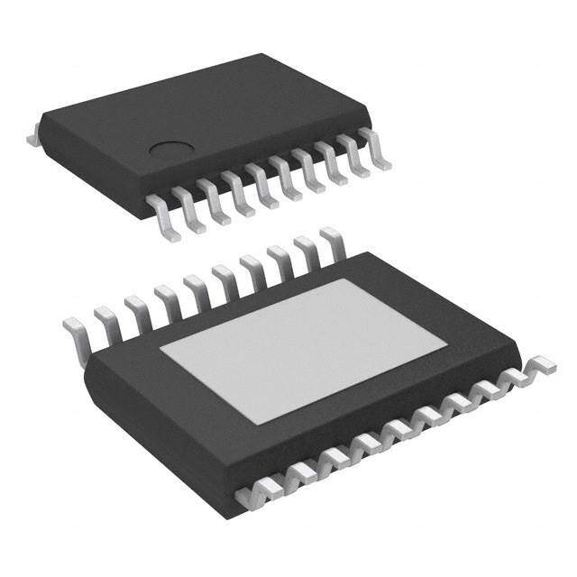
| 供应商器件封装 | 20-HTSSOP |
| 其它名称 | 296-10952-1 |
| 包装 | 剪切带 (CT) |
| 单位重量 | 81.800 mg |
| 同步整流器 | 无 |
| 商标 | Texas Instruments |
| 安装类型 | 表面贴装 |
| 安装风格 | SMD/SMT |
| 宽度 | 4.4 mm |
| 封装 | Reel |
| 封装/外壳 | 20-TSSOP(0.173",4.40mm 宽)裸焊盘 |
| 封装/箱体 | HTSSOP-20 |
| 工作温度 | -40°C ~ 85°C |
| 工作温度范围 | - 40 C to + 85 C |
| 工厂包装数量 | 2000 |
| 开关频率 | 320 kHz |
| 拓扑结构 | Boost |
| 最大工作温度 | + 85 C |
| 最大输入电压 | 3.6 V |
| 最小工作温度 | - 40 C |
| 最小输入电压 | 1.8 V |
| 标准包装 | 1 |
| 电压-输入 | 1.8 V ~ 3.6 V |
| 电压-输出 | 5V |
| 电流-输出 | 100mA |
| 类型 | 升压(升压),切换电容(充电泵) |
| 系列 | TPS60140 |
| 输入电压 | 1.8 V to 3.6 V |
| 输出数 | 1 |
| 输出电压 | 5 V |
| 输出电流 | 100 mA |
| 输出端数量 | 1 Output |
| 输出类型 | 固定 |
| 配用 | /product-detail/zh/TPS60140EVM-144/296-10951-ND/381813 |
| 频率-开关 | 320kHz |


- 商务部:美国ITC正式对集成电路等产品启动337调查
- 曝三星4nm工艺存在良率问题 高通将骁龙8 Gen1或转产台积电
- 太阳诱电将投资9.5亿元在常州建新厂生产MLCC 预计2023年完工
- 英特尔发布欧洲新工厂建设计划 深化IDM 2.0 战略
- 台积电先进制程称霸业界 有大客户加持明年业绩稳了
- 达到5530亿美元!SIA预计今年全球半导体销售额将创下新高
- 英特尔拟将自动驾驶子公司Mobileye上市 估值或超500亿美元
- 三星加码芯片和SET,合并消费电子和移动部门,撤换高东真等 CEO
- 三星电子宣布重大人事变动 还合并消费电子和移动部门
- 海关总署:前11个月进口集成电路产品价值2.52万亿元 增长14.8%


PDF Datasheet 数据手册内容提取
Product Sample & Technical Tools & Support & Folder Buy Documents Software Community TPS60140,TPS60141 SLVS273A–FEBRUARY2000–REVISEDNOVEMBER2015 TPS6014x Low Power DC-DC Converter Regulated 5-V, 100-mA Charge Pump Voltage Tripler 1 Features 3 Description • Regulated5V ±4%OutputVoltage The TPS6014x step-up, regulated charge pumps 1 generate a 5-V ±4% output voltage from a 1.8-V to • Upto100-mAOutputCurrent 3.6-V input voltage range. The devices are typically • 1.8-Vto3.6-VInputVoltageRange powered by two alkaline, NiCd, or NiMH battery cells • 65-µAQuiescentSupplyCurrent and provide an output current of minimum 100 mA from a 2-V input. Only four external capacitors are • 0.05-µAShutdownCurrent,BatteryIsIsolated needed to build a complete voltage tripler charge FromLoadinShutdown pump. • IntegratedLow-BatteryorPower-GoodIndicator The devices regulate the output by using the pulse- • Low-OutputVoltageRippleOverCompleteOutput skip topology. The controller is optimized for lowest CurrentRange output voltage ripple over the complete output current • Easy-to-DesignWithLow-EMIPowerSupply range. The output peak current and therefore the BecauseNoInductorsAreRequired output voltage ripple are drastically reduced compared to a conventional pulse-skip topology by • EvaluationModuleAvailable(TPS60140EVM-144) regulating the charge pump output resistance. At light • Availableina6.5-mm ×4.4-mm20-PinHTSSOP loads the maximum output resistance is limited to Package assurealowquiescentcurrent. 2 Applications The TPS60140 includes a low-battery comparator that issues a warning if the battery voltage drops • ReplacementofDC-DCConvertersWithInductors below a user-adjustable threshold voltage. The inBattery-PoweredApplications: TPS60141 features a power-good output that goes – TwoBatteryCellsto5-VConversions active when the output voltage reaches 90% of its nominalvalue. – PortableInstruments – MiniatureEquipment DeviceInformation(1) – Backup-BatteryBoostConverters PARTNUMBER PACKAGE BODYSIZE(NOM) – MedicalInstruments TPS6014x HTSSOP(20) 6.50mm×4.40mm – 5-VSmartCardSupplies (1) For all available packages, see the orderable addendum at theendofthedatasheet. TypicalApplicationSchematic EfficiencyvsOutputCurrent Input TPS60140 Output 1.8 V to 3.6 V 5V,100mA 90 IN OUT Co R1 IN FB 10µF 80 VI= 2.0 V R3 Low R2 LBI LBO Battery VI= 2.4 V 70 Warning % Ci C1+ C2+ C2 y− VI= 2.7 V 4.7µF c C1 C1− C2− 2.2µF en 60 2.2µF fici ENABLE NC Ef 50 PGND GND OFF/ON 40 30 0.1 1 10 100 1000 IO−Output Current−mA 1 An IMPORTANT NOTICE at the end of this data sheet addresses availability, warranty, changes, use in safety-critical applications, intellectualpropertymattersandotherimportantdisclaimers.PRODUCTIONDATA.
TPS60140,TPS60141 SLVS273A–FEBRUARY2000–REVISEDNOVEMBER2015 www.ti.com Table of Contents 1 Features.................................................................. 1 9.4 DeviceFunctionalModes........................................10 2 Applications........................................................... 1 10 ApplicationandImplementation........................ 11 3 Description............................................................. 1 10.1 ApplicationInformation..........................................11 4 RevisionHistory..................................................... 2 10.2 TypicalApplication ...............................................11 5 Description(continued)......................................... 3 11 PowerSupplyRecommendations..................... 15 6 DeviceComparisonTable..................................... 4 12 Layout................................................................... 15 12.1 LayoutGuidelines.................................................15 7 PinConfigurationandFunctions......................... 4 12.2 LayoutExample....................................................15 8 Specifications......................................................... 5 12.3 PowerDissipation.................................................15 8.1 AbsoluteMaximumRatings......................................5 13 DeviceandDocumentationSupport................. 17 8.2 ESDRatings ............................................................5 13.1 DeviceSupport......................................................17 8.3 RecommendedOperatingConditions.......................5 13.2 DocumentationSupport........................................17 8.4 ThermalInformation..................................................5 13.3 RelatedLinks........................................................17 8.5 ElectricalCharacteristics...........................................6 13.4 Trademarks...........................................................17 8.6 TypicalCharacteristics..............................................6 13.5 ElectrostaticDischargeCaution............................17 9 DetailedDescription.............................................. 7 13.6 Glossary................................................................17 9.1 Overview...................................................................7 14 Mechanical,Packaging,andOrderable 9.2 FunctionalBlockDiagrams.......................................7 Information........................................................... 17 9.3 FeatureDescription...................................................8 4 Revision History NOTE:Pagenumbersforpreviousrevisionsmaydifferfrompagenumbersinthecurrentversion. ChangesfromOriginal(February2000)toRevisionA Page • AddedESDRatingstable,FeatureDescriptionsection,DeviceFunctionalModes,ApplicationandImplementation section,PowerSupplyRecommendationssection,Layoutsection,DeviceandDocumentationSupportsection,and Mechanical,Packaging,andOrderableInformationsection ................................................................................................. 1 2 SubmitDocumentationFeedback Copyright©2000–2015,TexasInstrumentsIncorporated ProductFolderLinks:TPS60140 TPS60141
TPS60140,TPS60141 www.ti.com SLVS273A–FEBRUARY2000–REVISEDNOVEMBER2015 5 Description (continued) The logic shutdown function disables the converter, reduces the supply current to a maximum of 1 µA and disconnects the output from the input. Special current-control circuitry prevents excessive current from being drawn from the battery during start-up. This DC/DC converter requires no inductors, therefore, EMI is of little concern. The TPS6014x operates over a free-air temperature range of –40°C to 85°C. It is available in the small, thermallyenhanced20-pinHTSSOPpackage(PWP). Copyright©2000–2015,TexasInstrumentsIncorporated SubmitDocumentationFeedback 3 ProductFolderLinks:TPS60140 TPS60141
TPS60140,TPS60141 SLVS273A–FEBRUARY2000–REVISEDNOVEMBER2015 www.ti.com 6 Device Comparison Table PARTNUMBER PACKAGE PACKAGEDESIGNATOR DEVICEFEATURES TPS60140 Low-batterydetector 20-pinthermallyenhancedHTSSOP PWP 2-cellto5V,100mA TPS60141 Power-gooddetector 7 Pin Configuration and Functions PWPPackage(TPS60140) 20Pin-HTSSOP PWPPackage(TPS60141) TopView 20Pin-HTSSOP TopView GND 1 20 GND GND 1 20 GND GND 2 19 GND GND 2 19 GND ENABLE 3 18 LBI ENABLE 3 18 NC FB 4 17 LBO FB 4 17 PG OUT 5 16 NC OUT 5 16 NC C1+ 6 15 C2+ C1+ 6 15 C2+ IN 7 14 IN IN 7 14 IN C1− 8 13 C2− C1− 8 13 C2− PGND 9 12 PGND PGND 9 12 PGND PGND 10 11 PGND PGND 10 11 PGND PinFunctions PIN I/O DESCRIPTION NAME NO. C1+ 6 — PositiveterminaloftheflyingcapacitorC1 C1− 8 — NegativeterminaloftheflyingcapacitorC1 C2+ 15 — PositiveterminaloftheflyingcapacitorC2 C2− 13 — NegativeterminaloftheflyingcapacitorC2 ENABLEinput.ConnectENABLEtoINfornormaloperation.WhenENABLEisalogiclow,thedeviceturnsoffandthe ENABLE 3 I supplycurrentdecreasesto0.05µA.Theoutputisdisconnectedfromtheinputwhenthedeviceisplacedinshutdown. Feedbackinput.ConnectFBtoOUTasclosetotheloadaspossibletoachievebestregulation.Aresistivedividerisonthe FB 4 I chiptomatchtheoutputvoltagetotheinternalreferencevoltageof1.21V. 1,2,19, GND — Ground.Analoggroundforinternalreferenceandcontrolcircuitry.ConnecttoPGNDthroughashorttrace. 20 IN 7,14 I Supplyinput.BypassINtoPGNDwithcapacitorCIN.ConnectbothINterminalsthroughashorttrace. Lowbatterydetectoroutput(TPS60140)orpowergoodoutput(TPS60141).Open-drainoutputofthelow-batteryindicatoror LBO/PG 17 O power-goodcomparator.Itcansink1mA.TIrecommendsa100-kΩto1-MΩpullup.Leavetheterminalunconnectedifthe low-batteryorpower-gooddetectorfunctionisnotused. Lowbatterydetectorinput(TPS60140only).Thevoltageappliedtothisterminaliscomparedtotheinternal1.21-Vreference LBI/NC 18 I voltage.Connecttheterminaltogroundifthelow-batterycomparatorisnotused.OntheTPS60141,thisterminalisnot connectedtothechipandshouldremainunconnected. NC 16 — Notconnected OUT 5 O Regulated5-Vpoweroutput.BypassOUTtoPGNDwiththeoutputfiltercapacitorCOUT. PGND 9−12 — Powerground.Thecharge-pumpcurrentflowsthroughthisterminal.ConnectallPGNDterminalstogether. 4 SubmitDocumentationFeedback Copyright©2000–2015,TexasInstrumentsIncorporated ProductFolderLinks:TPS60140 TPS60141
TPS60140,TPS60141 www.ti.com SLVS273A–FEBRUARY2000–REVISEDNOVEMBER2015 8 Specifications 8.1 Absolute Maximum Ratings overoperatingfree-airtemperaturerange(unlessotherwisenoted) (1)(2) MIN MAX UNIT SupplyvoltageatINtoGNDandPGND −0.3 3.6 V VoltageatOUT,ENABLE,LBI,LBO,PG,FBtoGNDandPGND −0.3 5.4 V VoltageatC1+toGND −0.3 V +0.3 V OUT VoltageatC1–toGND −0.3 V +0.3 V IN VoltageatC2+toGND −0.3 V +0.3 V OUT VoltageatC2–toGND −0.3 V +0.3 V IN Continuousoutputcurrent 150 mA T Maximumjunctiontemperature 150 °C J T Storagetemperature –55 150 °C stg (1) StressesbeyondthoselistedunderAbsoluteMaximumRatingsmaycausepermanentdamagetothedevice.Thesearestressratings only,whichdonotimplyfunctionaloperationofthedeviceattheseoranyotherconditionsbeyondthoseindicatedunderRecommended OperatingConditions.Exposuretoabsolute-maximum-ratedconditionsforextendedperiodsmayaffectdevicereliability. (2) V ,V ,V ,andV canexceedV uptothemaximumratedvoltagewithoutincreasingtheleakagecurrentdrawnby (ENABLE) (LBI) (LBO) (PG) IN theseinputs. 8.2 ESD Ratings VALUE UNIT Human-bodymodel(HBM),perANSI/ESDA/JEDECJS-001(1) ±2000 V(ESD) Electrostaticdischarge Charged-devicemodel(CDM),perJEDECspecificationJESD22- V C101(2) ±500 (1) JEDECdocumentJEP155statesthat500-VHBMallowssafemanufacturingwithastandardESDcontrolprocess. (2) JEDECdocumentJEP157statesthat250-VCDMallowssafemanufacturingwithastandardESDcontrolprocess. 8.3 Recommended Operating Conditions overoperatingfree-airtemperaturerange(unlessotherwisenoted) MIN NOM MAX UNIT V Inputvoltage 1.8 3.6 V IN I max Continuousoutputcurrent 100 mA O T Operatingjunctiontemperature 125 °C J 8.4 Thermal Information TPS60140, TPS60141 THERMALMETRIC(1) UNIT PWP(HTSSOP) 20PINS R Junction-to-ambientthermalresistance 42 °C/W θJA R Junction-to-case(top)thermalresistance 23 °C/W θJC(top) R Junction-to-boardthermalresistance 20 °C/W θJB ψ Junction-to-topcharacterizationparameter 0.6 °C/W JT ψ Junction-to-boardcharacterizationparameter 20 °C/W JB R Junction-to-case(bottom)thermalresistance 1.6 °C/W θJC(bot) (1) Formoreinformationabouttraditionalandnewthermalmetrics,seetheSemiconductorandICPackageThermalMetricsapplication report,SPRA953. Copyright©2000–2015,TexasInstrumentsIncorporated SubmitDocumentationFeedback 5 ProductFolderLinks:TPS60140 TPS60141
TPS60140,TPS60141 SLVS273A–FEBRUARY2000–REVISEDNOVEMBER2015 www.ti.com 8.5 Electrical Characteristics C =4.7µF,C1=C2=2.2µF,C =10µF(1)atT =−40°Cto85°C,V =2V,FB=V andENABLE=V (unless IN OUT C IN OUT IN otherwisenoted) PARAMETER TESTCONDITIONS MIN TYP MAX UNIT V(UVLO) Undervoltagelockoutthreshold TC=25°C 1.6 1.8 V IOmax Maximumcontinuousoutputcurrent 100 mA 1.8V<VIN<2V,VOUT,Start-up=5V, 4.8 5.2 VO Outputvoltage 0<IOUT<IOmax/2,TC=0°Cto70°C V 2V<VIN<3.6V,0<IOUT<IOmax 4.8 5.2 Ilkg(OUT) Outputleakagecurrent VIN=2.4V,V(ENABLE)=GND 1 µA IQ Quiescentcurrent(no-loadinputcurrent) VIN=2.4V 65 90 µA I(SD) Shutdowncurrent VIN=2.4V,V(ENABLE)=GND 0.05 1 µA f(OSC) Oscillatorfrequency 210 320 450 kHz VIL ENABLEinputvoltagelow VIN=1.8V 0.3×VI V VIH ENABLEinputvoltagehigh VIN=3.6V 0.7×VI V Ilkg(ENABLE) ENABLEinputleakagecurrent V(ENABLE)=GNDorVIN 0.01 0.1 µA Outputloadregulation VIN=2.4V,1mA<IOUT<IOUTmax, 0.003 %/mA TC=25°C Outputlineregulation 2V<VIN<3.6V,VOUT=5V: 0.08 %/V IOUT=75mA,TC=25°C I(SC) Short-circuitcurrentlimit VIN<2.4V,VOUT=0V,TC=25°C 100 mA VIN=1.8Vto2.2V, V(TRIP,LBI) LBItripvoltage TPS60140 Hysteresis0.8%forrisingLBIvoltage, 1.15 1.21 1.27 V TC=0°Cto70°C IIN(LBI) LBIinputcurrent TPS60140 LBI=1.3V 20 100 nA VOUT(LBO) LBOoutputvoltagelow(2) TPS60140 V(LBI)=0V,I(LBO,SINK)=1mA 0.4 v Ilkg(LBO) LBOoutputleakagecurrent TPS60140 V(LBI)=1.3V,V(LBO)=5V 0.01 0.1 µA V(TRIP,PG) Power-goodtripvoltage TPS60141 TC=0°Cto70°C 0.86×VO 0.90×VO 0.94×VO V Power-goodtripvoltage Vhys(PG) hysteresis TPS60141 VOUTrampingdown,TC=0°Cto70°C 0.80% VOUT(PG) Power-goodoutputvoltagelow TPS60141 VOUT=0V,I(PG,SINK)=1mA 0.4 V Ilkg(PG) Power-goodleakagecurrent TPS60141 VOUT=5V,V(PG)=5V 0.01 0.1 µA (1) AllcapacitorsareceramiccapacitorsofthetypeX5RorX7R. (2) Duringstart-uptheLBOsignalisinvalidforthefirst500µs. 8.6 Typical Characteristics 75 330 70 TA= 85°C Hz 325 TA=−40°C A k µ−Supply Current−C 6605 TA= 25°C TA=−40°C Oscillator Frequency− 333112050 TA= 85°C TA= 25°C C − I 55 OSC) 305 f( 50 300 1.8 2.0 2.2 2.4 2.6 2.8 3.0 3.2 3.4 3.6 1.8 2.0 2.2 2.4 2.6 2.8 3.0 3.2 3.4 3.6 VI−InputVoltage−V VI−InputVoltage−V Figure1.QuiescentSupplyCurrentvsInputVoltage Figure2.OscillatorFrequencyvsInputVoltage 6 SubmitDocumentationFeedback Copyright©2000–2015,TexasInstrumentsIncorporated ProductFolderLinks:TPS60140 TPS60141
TPS60140,TPS60141 www.ti.com SLVS273A–FEBRUARY2000–REVISEDNOVEMBER2015 9 Detailed Description 9.1 Overview The TPS6014x devices regulate the output voltage using an improved pulse-skip topology. In pulse-skip mode the error amplifier disables switching of the power stages when it detects an output voltage higher than 5 V. The oscillator halts and the controller skips switching cycles. The error amplifier reactivates the oscillator and starts switching of the power stages again when the output voltage drops below 5 V. The output resistance of the chargepumpiscontrolledtoimprovetherippleperformance.Thislimitstheoutputcurrenttotheminimumthatis necessary to sustain a regulated output voltage. The benefit is that the ripple performance is nearly as good as withalinear-regulationtopology. At light loads a conventional pulse-skip regulation mode is used, but the charge pump output resistance is held at a high level. The pulse-skip regulation minimizes the operating current because the charge pump does not switch continuously and hence the gate-charge losses of the MOSFETs are reduced. Additionally, all functions except voltage reference, error amplifier, and low-battery or power-good comparator are deactivated when the output is higher than 5 V. When switching is disabled by the error amplifier, the load is also isolated from the input.Thisimprovedpulse-skipcontroltopologyisalsoreferredtoas active-cyclecontrol. 9.2 Functional Block Diagrams TPS60140 IN Oscillator C1+ C1 C1− PGND _ ChargePump IN Power Stage C2+ Control + ENABLE Circuit + C2 VREF − C2− OUT PGND FB LBO _ _ Shutdown/ LBI Start-up Control + + + + − 0.8× VI − VREF GND Figure3. TPS60140FunctionalBlockDiagram Copyright©2000–2015,TexasInstrumentsIncorporated SubmitDocumentationFeedback 7 ProductFolderLinks:TPS60140 TPS60141
TPS60140,TPS60141 SLVS273A–FEBRUARY2000–REVISEDNOVEMBER2015 www.ti.com Functional Block Diagrams (continued) TPS60141 IN Oscillator C1+ C1 C1− PGND _ Charge Pump IN Power Stage C2+ Control + ENABLE Circuit + C2 VREF − C2− OUT PGND FB PG _ _ Shutdown/ Start-up Control + + + + − 0.8× VI VREF − GND Figure4. TPS60141FunctionalBlockDiagram 9.3 Feature Description 9.3.1 UndervoltageLockout The TPS6014x devices have an undervoltage lockout feature that deactivates the device and places it in shutdownmodewhentheinputvoltagefallsbelow1.6V. 9.3.2 Low-BatteryDetector(TPS60140Only) The internal low-battery comparator trips at 1.21 V ± 5% when the voltage on pin LBI ramps down. The voltage V atwhichthelowbatterywarningisissuedcanbeadjustedwitharesistivedividerasshowninFigure5.TI (TRIP) recommends that the sum of resistors R1 and R2 to be in the 100-kΩ to 1-MΩ range. When choosing R1 and R2,beawareoftheinputleakagecurrentintotheLBIterminal. LBO is an open-drain output. TI recommends an external pullup resistor to OUT, in the 100-kΩ to 1-MΩ range. During start-up, the LBO output signal is invalid for the first 500 µs. LBO is high impedance when the device is disabled.Ifthelow-batterycomparatorfunctionisnotused,connectLBItogroundandleaveLBOunconnected. 8 SubmitDocumentationFeedback Copyright©2000–2015,TexasInstrumentsIncorporated ProductFolderLinks:TPS60140 TPS60141
TPS60140,TPS60141 www.ti.com SLVS273A–FEBRUARY2000–REVISEDNOVEMBER2015 Feature Description (continued) VO R3 IN VBAT LBO R1 LBI _ æ R1ö + V(TRIP) =1.21V´ç1+ ÷ è R2ø R2 + VREF − Figure5. ProgrammingoftheLow-BatteryComparatorTripVoltage A 100-nF ceramic capacitor should be connected in parallel to R2 if large line transients are expected. These voltage drops can inadvertently trigger the low-battery comparator and produce a wrong low-battery warning signalattheLBOpin. Formulastocalculatetheresistivedividerforlowbatterydetection,withV =1.15Vto1.27V: (LBI) V R2=1MW´ LBI V BAT (1) R1=1MW-R2 (2) Formulastocalculatetheminimumandmaximumtripvoltage: R1 +R2 V = V ´ (min) (max) trip(min) LBI(min) R2 (max) (3) R1 +R2 V = V ´ (man) (mix) trip(man) LBI(man) R2 (mix) (4) Table1.RecommendedValuesfortheResistiveDividerFromtheE96Series (±1%) V/V R1/kΩ R2/kΩ V MIN/V V MAX/V I (TRIP) (TRIP) 1.8 357 732 1.700 1.902 1.9 365 634 1.799 2.016 2 412 634 1.883 2.112 2.1 432 590 1.975 2.219 2.2 442 536 2.08 2.338 9.3.3 Power-GoodDetector(TPS60141) The power-good (PG) terminal is an open-drain output that is pulled low when the output is out of regulation. When the output rises to typically 90% of its nominal voltage, the power-good output is released. Power-good is highimpedanceinshutdown.InnormaloperationanexternalpullupresistormustbeconnectedbetweenPGand OUT. The resistor should be in the 100-kΩ to 1-MΩ range. If the power-good function is not used, the PG terminalshouldremainunconnected. Copyright©2000–2015,TexasInstrumentsIncorporated SubmitDocumentationFeedback 9 ProductFolderLinks:TPS60140 TPS60141
TPS60140,TPS60141 SLVS273A–FEBRUARY2000–REVISEDNOVEMBER2015 www.ti.com 9.4 Device Functional Modes 9.4.1 Start-UpProcedureandShutdown During start-up (that is, when ENABLE is set from logic low to logic high), the output capacitor is charged up with a limited current until the output voltage (V ) reaches 0.8 × V. When the start-up comparator detects this voltage O I limit, the IC begins switching. This precharging of the output capacitor ensures a short start-up time. In addition, the inrush current into an empty output capacitor is limited because the current through the switches is limited beforethechargepumpstartsswitching. Driving ENABLE low places the device in shutdown mode. This disables all switches, the oscillator, and control logic. The device typically draws 0.05 µA of supply current in this mode. Leakage current drawn from the output isaslowas1µA(maximum).ThedeviceexitsshutdownonceENABLEissettoahighlevel.Whenthedeviceis inshutdown,theloadisisolatedfromtheinput. 9.4.2 Short-CircuitProtection The TPS6014x devices are also short-circuit protected. The output current is limited to typically 100 mA during a hard short-circuit condition at the output; that is, when V is GND. In this case, the condition to enter the start- OUT up mode is met, the device stops switching and controls the on-resistance of the appropriate MOSFET switches tolimitthecurrent. 10 SubmitDocumentationFeedback Copyright©2000–2015,TexasInstrumentsIncorporated ProductFolderLinks:TPS60140 TPS60141
TPS60140,TPS60141 www.ti.com SLVS273A–FEBRUARY2000–REVISEDNOVEMBER2015 10 Application and Implementation NOTE Information in the following applications sections is not part of the TI component specification, and TI does not warrant its accuracy or completeness. TI’s customers are responsible for determining suitability of components for their purposes. Customers should validateandtesttheirdesignimplementationtoconfirmsystemfunctionality. 10.1 Application Information The TPS6014x charge pumps provide a regulated 5-V output from a 1.8-V to 3.6-V input voltage range. They candeliveramaximumcontinuousloadcurrentofatleast100mAatV =2Vminimum. I 10.2 Typical Application Input TPS60140 Output 1.8 V to 3.6 V 5V,100mA IN OUT Co R1 IN FB 10µF R3 Low R2 LBI LBO Battery Warning Ci C1+ C2+ C2 4.7µF 2.2µF C1 C1− C2− 2.2µF ENABLE NC PGND GND OFF/ON Figure6. TypicalApplicationSchematic 10.2.1 DesignRequirements Designed specifically for space-critical battery-powered applications, the complete charge pump circuit requires only four external capacitors. The design guideline provides a component selection to operate the device within theRecommendedOperatingConditions. Table2showsthelistofcomponentsfortheApplicationCurves. Table2.ComponentsforApplicationCurves REFERENCE VALUE DESCRIPTION MANUFACTURER PARTNUMBER C1,C2 2.2µF Ceramicflyingcapacitors TaiyoYuden EMK316BJ225KL-T C 4.7µF Ceramicinputcapacitor TaiyoYuden LMK316BJ475KL-T IN C 10µF Ceramicoutputcapacitor TaiyoYuden JMK316BJ106ML-T OUT LBIinputvoltage R1 357kΩ E96-Series adjustment LBIinputvoltage R2 619kΩ E96-Series adjustment Pullupresistorforthe R3 1MΩ open-drainoutputLBO Copyright©2000–2015,TexasInstrumentsIncorporated SubmitDocumentationFeedback 11 ProductFolderLinks:TPS60140 TPS60141
TPS60140,TPS60141 SLVS273A–FEBRUARY2000–REVISEDNOVEMBER2015 www.ti.com 10.2.2 DetailedDesignProcedure 10.2.2.1 CapacitorSelection The capacitance values of the TPS6014x external capacitors are closely linked to the output current and output ripple requirements. For lowest ripple, low ESR (< 0.1 Ω) capacitors should be used at the input and output of thechargepump. The input capacitor improves system efficiency by reducing the input impedance. It also stabilizes the input current of the power source. The input capacitor should be chosen according to the power supply used and the distance from the power source to the converter IC. The input capacitor selection also depends on the output ripple requirements. C is recommended to be about 2-times to 4-times as large as the flying capacitors. The IN lowertheESRoftheinputcapacitorC ,theloweristheoutputripple. IN The output capacitor C can be selected from 2× to 50× larger than the flying capacitor, depending on the OUT rippletolerance.ThelargerC andtheloweritsESR,thelowerwillbetheoutputvoltageripple. OUT Generally, the flying capacitors will be the smallest. Only ceramic capacitors are recommended because of their low ESR and because they retain their capacitance at the switching frequency. Be aware that, depending on the material used to manufacture them, ceramic capacitors might lose their capacitance over temperature and voltage. Ceramic capacitors of type X7R or X5R material will keep their capacitance over temperature and voltage, whereas Z5U or Y5V-type capacitors will decrease in capacitance. Table 3 lists recommended capacitor values. Table3.RecommendedCapacitorValues I C C C V TYP OUT IN (xF) OUT PP (mA) (µF) (µF) (µF) (mV) 0−50 4.7 2.2 4.7 40 0−100 4.7 2.2 10 40 0−100 4.7 2.2 22 18 If the measured output voltage ripple is too high for the application, improvements can be made. The first step is to increase the capacitance at the output. If the ripple is still too high, the second step would be to increase the capacitance at the input. For lower output currents, lower value flying capacitors can be used. Table 3 and Table4liststhemanufacturersofrecommendedcapacitors. Table4.RecommendedCapacitors(1) MANUFACTURER PARTNUMBER CAPACITANCE CASESIZE TYPE LMK212BJ105KG−T 1µF 805 Ceramic EMK316BJ225KL−T 2.2µF 1206 Ceramic LMK212BJ225MG−T 2.2µF 805 Ceramic TaiyoYuden LMK316BJ475KL−T 4.7µF 1206 Ceramic JMK316BJ106ML–T 10µF 1206 Ceramic LMK325BJ106MN−T 10µF 1210 Ceramic LMK432226MM−T 22µF 1812 Ceramic 0805ZC105KAT2A 1µF 805 Ceramic AVX 1206ZC225KAT2A 2.2µF 1206 Ceramic (1) Note:CasecodecompatibilitywithEIA535BAACandCECC30801moldedchips. Table5.RecommendedCapacitorManufacturers MANUFACTURER CAPACITORTYPE INTERNETSITE TaiyoYuden X7R/X5Rceramic http://www.t−yuden.com/ AVX X7R/X5Rceramic http://www.avxcorp.com/ 12 SubmitDocumentationFeedback Copyright©2000–2015,TexasInstrumentsIncorporated ProductFolderLinks:TPS60140 TPS60141
TPS60140,TPS60141 www.ti.com SLVS273A–FEBRUARY2000–REVISEDNOVEMBER2015 10.2.3 ApplicationCurves 90 90 IO= 50 mA 80 VI= 2.0 V 80 VI= 2.4 V % 70 % Efficiency− 60 VI= 2.7 V Efficiency− 6700 50 50 40 30 40 0.1 1 10 100 1000 1.8 2.0 2.2 2.4 2.6 2.8 3.0 3.2 3.4 3.6 IO−Output Current−mA VI−InputVoltage−V Figure7.EfficiencyvsOutputCurrent Figure8.EfficiencyvsInputVoltage 5.10 5.10 IO= 1 mA 5.05 5.05 V e− 5.00 −V 5.00 put Voltag 4.95 VI= 2.4 V VI= 2.7 V VI= 3.6 V ut Voltage 4.95 IO= 100 mA IO= 50 mA Out VI= 1.8 V utp −O 4.90 −O 4.90 V O V 4.85 4.85 4.80 4.80 0.1 1 10 100 1000 1.8 2.0 2.2 2.4 2.6 2.8 3.0 3.2 3.4 3.6 IO−Output Current−mA VI−InputVoltage−V Figure9.OutputVoltagevsOutputCurrent Figure10.OutputVoltagevsInputVoltage 5.25 5.25 5.20 VIOI== 21. 4m VA 5.20 VIOI== 21.04 mVA V5.15 V5.15 OutputVoltage−555...100050 OutputVoltage−555...100050 V−O4.95 V−O4.95 4.90 4.90 4.85 4.85 0 50 100 150 200 250 300 350 400 450 500 0 5 10 15 20 25 30 35 40 45 50 t−Time−µs t−Time−µs Figure11.OutputVoltageRipple Figure12.OutputVoltageRipple Copyright©2000–2015,TexasInstrumentsIncorporated SubmitDocumentationFeedback 13 ProductFolderLinks:TPS60140 TPS60141
TPS60140,TPS60141 SLVS273A–FEBRUARY2000–REVISEDNOVEMBER2015 www.ti.com 5.13 60 VI= 2.4 V V 5.11 IO= 100 mA me− 50 IO= 100 mA d ge−V 55..0097 Amplitu 40 V−OutputVoltaO 55..0053 utVoltageRipple 2300 IO= 10 mA 5.01 utp IO= 1 mA O 4.99 −p 10 Vp 4.97 0 0 2 4 6 8 10 12 14 16 18 20 1.8 2.0 2.2 2.4 2.6 2.8 3.0 3.2 3.4 3.6 t−Time−µs VI−InputVoltage−V Figure13.OutputVoltageRipple Figure14.OutputVoltageRippleAmplitudevs InputVoltage 60 V V VI= 2.4 V − VI= 2.4 V m e − 50 ag de olt u V 5.07 Amplit 40 Output 5.05 Ripple 30 V−O5.03 e g Volta 20 −mA V−Outputpp 10 utput Current 260 0 O 0 0 10 20 30 40 50 60 70 80 90 100 −O 0 2 4 6 8 10 12 14 16 18 20 IO−Output Current−mA I t−Time−ms Figure15.OutputVoltageRippleAmplitudevs Figure16.LoadTransientResponse OutputCurrent V 6 6 − ge VI= 2.4 V Volta IO= 50 mA 5 IO= 100 mA 5 ut Out −Outp 5.07 ge−V 4 4 −V VO 55..0053 utVolta 3 Enable 3 Voltage Voltage−V 3.0 V−OutpO 12 12 Enable ut np 0 0 I 2.5 − VI −1 −1 2.00 2 4 6 8 10 12 14 16 18 20 −0.1 0.0 0.1 0.2 0.3 0.4 0.5 0.6 t−Time−ms t−Time−ms Figure17.LineTransientResponse Figure18.OutputVoltagevsTime(Start-UpTiming) 14 SubmitDocumentationFeedback Copyright©2000–2015,TexasInstrumentsIncorporated ProductFolderLinks:TPS60140 TPS60141
TPS60140,TPS60141 www.ti.com SLVS273A–FEBRUARY2000–REVISEDNOVEMBER2015 11 Power Supply Recommendations The TPS6014x devices have no special requirements for its input power supply. The input power supply's output currentmustberatedaccordingtothesupplyvoltage,outputvoltageandoutputcurrentoftheTPS6014x. 12 Layout 12.1 Layout Guidelines Careful board layout is necessary due to the high transient currents and switching frequency of the converter. All capacitors should be soldered in close proximity to the IC. Connect ground and power ground terminals through a short, low-impedance trace. A PCB layout proposal for a two-layer board is given in Figure 19. The bottom layer of the board carries only ground potential for best performance. The layout also provides improved thermal performanceastheexposedleadframeofthePowerPADpackageissolderedtothePCB. An evaluation module for the TPS60140 is available and can be ordered under product code TPS60140EVM−144.TheEVMusesthelayoutshowninFigure19. 12.2 Layout Example NOTE: Actualsizeis15mmx25mm. Figure19. RecommendedComponentPlacementandBoardLayout Table6.ComponentIdentification IC1 TPS6014x C1,C2 Flyingcapacitors C3,C6 Inputcapacitors C4,C5 Outputcapacitors C7 StabilizationcapacitorforLBI R1,R2 ResistivedividerforLBI R3 PullupresistorforLBO The best performance of the converter is achieved with additional bypass capacitors C5 and C6 at the input and output.CapacitorC7shouldbeincludedifthelargelinetransientsareexpected.Thecapacitorsarenotrequired. Theycanbeomittedinmostapplications. 12.3 Power Dissipation The power dissipated in the TPS6014x depends mainly on input voltage and output current and is described by Equation5: P =I ´(3´V -V ) (DISS) O I O (5) Copyright©2000–2015,TexasInstrumentsIncorporated SubmitDocumentationFeedback 15 ProductFolderLinks:TPS60140 TPS60141
TPS60140,TPS60141 SLVS273A–FEBRUARY2000–REVISEDNOVEMBER2015 www.ti.com Power Dissipation (continued) By observation of Equation 5, it can be seen that the power dissipation is worse for the highest input voltage V I andthehighestoutputcurrentI .Foraninputvoltageof3.6Vandanoutputcurrentof100mA,thecalculated OUT power dissipation P is 580 mW. This is also the point where the charge pump operates with its lowest (DISS) efficiency,whichisonly45%,andhencewiththehighestpowerlosses. P must be less than that allowed by the package rating. The thermal resistance junction to ambient of the (DISS) thermally enhanced TSSOP is 178°C/W for an unsoldered package. The thermal resistance junction to case, withtheexposedthermalpadsolderedtoaninfinitiveheatsink,is3.5°C/W. With the recommended maximum junction temperature of 125°C and an assumed maximum ambient operating temperature of 85°C, the maximum allowed thermal resistance junction to ambient of the system can be calculatedusingEquation6. T max-T 125°C-85°C R max = J A = =69°C/W qJA P max 580 mW (DISS) (6) Using a board layout as described in the application information section, R is typically 56°C/W for an θJA unsolderedPowerPAD™and41°C/WforasolderedPowerPAD. For more information, refer to the PowerPAD application report, PowerPAD™ Thermally Enhanced Package (SLMA002). 16 SubmitDocumentationFeedback Copyright©2000–2015,TexasInstrumentsIncorporated ProductFolderLinks:TPS60140 TPS60141
TPS60140,TPS60141 www.ti.com SLVS273A–FEBRUARY2000–REVISEDNOVEMBER2015 13 Device and Documentation Support 13.1 Device Support 13.1.1 Third-PartyProductsDisclaimer TI'S PUBLICATION OF INFORMATION REGARDING THIRD-PARTY PRODUCTS OR SERVICES DOES NOT CONSTITUTE AN ENDORSEMENT REGARDING THE SUITABILITY OF SUCH PRODUCTS OR SERVICES OR A WARRANTY, REPRESENTATION OR ENDORSEMENT OF SUCH PRODUCTS OR SERVICES, EITHER ALONEORINCOMBINATIONWITHANYTIPRODUCTORSERVICE. 13.2 Documentation Support 13.2.1 RelatedDocumentation Forrelateddocumentationseethefollowing: • PowerPAD™ThermallyEnhancedPackage,SLMA002. • TPS6010x/TPS6011xChargePump,SLVA070. 13.3 Related Links The following table lists quick access links. Categories include technical documents, support and community resources,toolsandsoftware,andquickaccesstosampleorbuy. Table7.RelatedLinks TECHNICAL TOOLS& SUPPORT& PARTS PRODUCTFOLDER SAMPLE&BUY DOCUMENTS SOFTWARE COMMUNITY TPS60140 Clickhere Clickhere Clickhere Clickhere Clickhere TPS60141 Clickhere Clickhere Clickhere Clickhere Clickhere 13.4 Trademarks PowerPADisatrademarkofTexasInstruments. Allothertrademarksarethepropertyoftheirrespectiveowners. 13.5 Electrostatic Discharge Caution Thesedeviceshavelimitedbuilt-inESDprotection.Theleadsshouldbeshortedtogetherorthedeviceplacedinconductivefoam duringstorageorhandlingtopreventelectrostaticdamagetotheMOSgates. 13.6 Glossary SLYZ022—TIGlossary. Thisglossarylistsandexplainsterms,acronyms,anddefinitions. 14 Mechanical, Packaging, and Orderable Information The following pages include mechanical, packaging, and orderable information. This information is the most current data available for the designated devices. This data is subject to change without notice and revision of thisdocument.Forbrowser-basedversionsofthisdatasheet,refertotheleft-handnavigation. Copyright©2000–2015,TexasInstrumentsIncorporated SubmitDocumentationFeedback 17 ProductFolderLinks:TPS60140 TPS60141
PACKAGE OPTION ADDENDUM www.ti.com 6-Feb-2020 PACKAGING INFORMATION Orderable Device Status Package Type Package Pins Package Eco Plan Lead/Ball Finish MSL Peak Temp Op Temp (°C) Device Marking Samples (1) Drawing Qty (2) (6) (3) (4/5) TPS60140PWP ACTIVE HTSSOP PWP 20 70 Green (RoHS NIPDAU Level-2-260C-1 YEAR -40 to 85 TPS60140 & no Sb/Br) TPS60140PWPR ACTIVE HTSSOP PWP 20 2000 Green (RoHS NIPDAU Level-2-260C-1 YEAR -40 to 85 TPS60140 & no Sb/Br) TPS60140PWPRG4 ACTIVE HTSSOP PWP 20 2000 Green (RoHS NIPDAU Level-2-260C-1 YEAR -40 to 85 TPS60140 & no Sb/Br) TPS60141PWP ACTIVE HTSSOP PWP 20 70 Green (RoHS NIPDAU Level-2-260C-1 YEAR -40 to 85 TPS60141 & no Sb/Br) TPS60141PWPR ACTIVE HTSSOP PWP 20 2000 Green (RoHS NIPDAU Level-2-260C-1 YEAR -40 to 85 TPS60141 & no Sb/Br) (1) The marketing status values are defined as follows: ACTIVE: Product device recommended for new designs. LIFEBUY: TI has announced that the device will be discontinued, and a lifetime-buy period is in effect. NRND: Not recommended for new designs. Device is in production to support existing customers, but TI does not recommend using this part in a new design. PREVIEW: Device has been announced but is not in production. Samples may or may not be available. OBSOLETE: TI has discontinued the production of the device. (2) RoHS: TI defines "RoHS" to mean semiconductor products that are compliant with the current EU RoHS requirements for all 10 RoHS substances, including the requirement that RoHS substance do not exceed 0.1% by weight in homogeneous materials. Where designed to be soldered at high temperatures, "RoHS" products are suitable for use in specified lead-free processes. TI may reference these types of products as "Pb-Free". RoHS Exempt: TI defines "RoHS Exempt" to mean products that contain lead but are compliant with EU RoHS pursuant to a specific EU RoHS exemption. Green: TI defines "Green" to mean the content of Chlorine (Cl) and Bromine (Br) based flame retardants meet JS709B low halogen requirements of <=1000ppm threshold. Antimony trioxide based flame retardants must also meet the <=1000ppm threshold requirement. (3) MSL, Peak Temp. - The Moisture Sensitivity Level rating according to the JEDEC industry standard classifications, and peak solder temperature. (4) There may be additional marking, which relates to the logo, the lot trace code information, or the environmental category on the device. (5) Multiple Device Markings will be inside parentheses. Only one Device Marking contained in parentheses and separated by a "~" will appear on a device. If a line is indented then it is a continuation of the previous line and the two combined represent the entire Device Marking for that device. (6) Lead/Ball Finish - Orderable Devices may have multiple material finish options. Finish options are separated by a vertical ruled line. Lead/Ball Finish values may wrap to two lines if the finish value exceeds the maximum column width. Addendum-Page 1
PACKAGE OPTION ADDENDUM www.ti.com 6-Feb-2020 Important Information and Disclaimer:The information provided on this page represents TI's knowledge and belief as of the date that it is provided. TI bases its knowledge and belief on information provided by third parties, and makes no representation or warranty as to the accuracy of such information. Efforts are underway to better integrate information from third parties. TI has taken and continues to take reasonable steps to provide representative and accurate information but may not have conducted destructive testing or chemical analysis on incoming materials and chemicals. TI and TI suppliers consider certain information to be proprietary, and thus CAS numbers and other limited information may not be available for release. In no event shall TI's liability arising out of such information exceed the total purchase price of the TI part(s) at issue in this document sold by TI to Customer on an annual basis. Addendum-Page 2
PACKAGE MATERIALS INFORMATION www.ti.com 16-Feb-2019 TAPE AND REEL INFORMATION *Alldimensionsarenominal Device Package Package Pins SPQ Reel Reel A0 B0 K0 P1 W Pin1 Type Drawing Diameter Width (mm) (mm) (mm) (mm) (mm) Quadrant (mm) W1(mm) TPS60140PWPR HTSSOP PWP 20 2000 330.0 16.4 6.95 7.1 1.6 8.0 16.0 Q1 TPS60141PWPR HTSSOP PWP 20 2000 330.0 16.4 6.95 7.1 1.6 8.0 16.0 Q1 PackMaterials-Page1
PACKAGE MATERIALS INFORMATION www.ti.com 16-Feb-2019 *Alldimensionsarenominal Device PackageType PackageDrawing Pins SPQ Length(mm) Width(mm) Height(mm) TPS60140PWPR HTSSOP PWP 20 2000 350.0 350.0 43.0 TPS60141PWPR HTSSOP PWP 20 2000 350.0 350.0 43.0 PackMaterials-Page2
None
None
None
IMPORTANTNOTICEANDDISCLAIMER TI PROVIDES TECHNICAL AND RELIABILITY DATA (INCLUDING DATASHEETS), DESIGN RESOURCES (INCLUDING REFERENCE DESIGNS), APPLICATION OR OTHER DESIGN ADVICE, WEB TOOLS, SAFETY INFORMATION, AND OTHER RESOURCES “AS IS” AND WITH ALL FAULTS, AND DISCLAIMS ALL WARRANTIES, EXPRESS AND IMPLIED, INCLUDING WITHOUT LIMITATION ANY IMPLIED WARRANTIES OF MERCHANTABILITY, FITNESS FOR A PARTICULAR PURPOSE OR NON-INFRINGEMENT OF THIRD PARTY INTELLECTUAL PROPERTY RIGHTS. These resources are intended for skilled developers designing with TI products. You are solely responsible for (1) selecting the appropriate TI products for your application, (2) designing, validating and testing your application, and (3) ensuring your application meets applicable standards, and any other safety, security, or other requirements. These resources are subject to change without notice. TI grants you permission to use these resources only for development of an application that uses the TI products described in the resource. Other reproduction and display of these resources is prohibited. No license is granted to any other TI intellectual property right or to any third party intellectual property right. TI disclaims responsibility for, and you will fully indemnify TI and its representatives against, any claims, damages, costs, losses, and liabilities arising out of your use of these resources. TI’s products are provided subject to TI’s Terms of Sale (www.ti.com/legal/termsofsale.html) or other applicable terms available either on ti.com or provided in conjunction with such TI products. TI’s provision of these resources does not expand or otherwise alter TI’s applicable warranties or warranty disclaimers for TI products. Mailing Address: Texas Instruments, Post Office Box 655303, Dallas, Texas 75265 Copyright © 2020, Texas Instruments Incorporated