ICGOO在线商城 > 集成电路(IC) > PMIC - 稳压器 - DC DC 开关稳压器 > TL2575HV-15IKTTR
 Datasheet下载
- 型号: TL2575HV-15IKTTR
- 制造商: Texas Instruments
- 库位|库存: xxxx|xxxx
- 要求:
| 数量阶梯 | 香港交货 | 国内含税 |
| +xxxx | $xxxx | ¥xxxx |
查看当月历史价格
查看今年历史价格
TL2575HV-15IKTTR产品简介:
ICGOO电子元器件商城为您提供TL2575HV-15IKTTR由Texas Instruments设计生产,在icgoo商城现货销售,并且可以通过原厂、代理商等渠道进行代购。 TL2575HV-15IKTTR价格参考¥9.84-¥20.07。Texas InstrumentsTL2575HV-15IKTTR封装/规格:PMIC - 稳压器 - DC DC 开关稳压器, 固定 降压 开关稳压器 IC 正 15V 1 输出 1A TO-263-6,D²Pak(5 引线 + 接片),TO-263BA。您可以下载TL2575HV-15IKTTR参考资料、Datasheet数据手册功能说明书,资料中有TL2575HV-15IKTTR 详细功能的应用电路图电压和使用方法及教程。
TL2575HV-15IKTTR 是由 Texas Instruments(德州仪器)生产的一款 PMIC - DC/DC 开关稳压器。该型号属于 TL2575 系列,是一款高电压、低功耗的降压型开关稳压器,能够将较高的输入电压转换为稳定的 1.5V 输出电压。以下是其主要应用场景:

 1. 便携式电子设备
   - TL2575HV-15IKTTR 的高效能和低功耗特性使其非常适合用于便携式电子设备,例如手持终端、移动电源、蓝牙设备等。
   - 在这些应用中,它能够从电池供电的高电压输入(如锂离子电池的 3.6V 或更高)转换为稳定的 1.5V 输出,为 MCU(微控制器)、传感器或其他低电压组件供电。

 2. 通信设备
   - 该稳压器可以应用于通信领域的低功耗模块,例如无线通信模块、射频前端电路等。
   - 它的高效率和小尺寸设计有助于减少热量生成,从而提高系统的整体性能和可靠性。

 3. 工业自动化
   - 在工业控制领域,TL2575HV-15IKTTR 可以为各种传感器、数据采集模块和小型嵌入式系统提供稳定的电源支持。
   - 其高压输入能力(最高可达 36V)使其能够在复杂的工业环境中工作,适应宽范围的输入电压波动。

 4. 消费类电子产品
   - 该芯片适用于需要低电压输出的消费类电子产品,例如数码相机、游戏控制器、智能家居设备等。
   - 它的小封装尺寸(SOT-23 封装)使得其易于集成到空间受限的设计中。

 5. 医疗设备
   - 在医疗领域,TL2575HV-15IKTTR 可用于便携式健康监测设备(如血糖仪、脉搏血氧仪)或可穿戴设备。
   - 其低功耗特性有助于延长电池寿命,同时确保设备的稳定运行。

 6. 汽车电子
   - 虽然 TL2575HV-15IKTTR 并非专为汽车级应用设计,但在某些非关键的汽车电子子系统中(如车内娱乐系统或传感器模块),它也可以作为电源解决方案使用。

 特性总结:
- 输入电压范围:4.5V 至 36V
- 固定输出电压:1.5V
- 最大输出电流:500mA
- 高效能:高达 90% 的转换效率
- 小尺寸封装:SOT-23

综上所述,TL2575HV-15IKTTR 主要应用于需要高效、低功耗、小尺寸电源解决方案的场景,尤其适合便携式设备、通信模块、工业自动化以及消费类电子产品等领域。
| 参数 | 数值 |
| 产品目录 | 集成电路 (IC)半导体 |
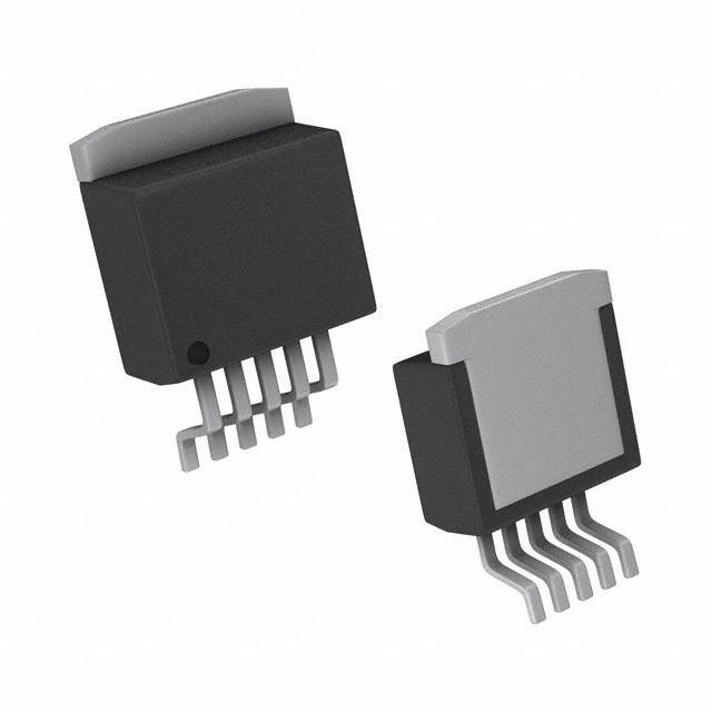
| 描述 | IC REG BUCK 15V 1A TO263稳压器—开关式稳压器 1-A Step-Down Vltge |
| 产品分类 | |
| 品牌 | Texas Instruments |
| 产品手册 | |
| 产品图片 |
|
| rohs | 符合RoHS无铅 / 符合限制有害物质指令(RoHS)规范要求 |
| 产品系列 | 电源管理 IC,稳压器—开关式稳压器,Texas Instruments TL2575HV-15IKTTR- |
| 数据手册 | |
| 产品型号 | TL2575HV-15IKTTR |
| PCN封装 | |
| PCN设计/规格 | |
| PWM类型 | - |
| 产品种类 | 稳压器—开关式稳压器 |
| 供应商器件封装 | DDPAK/TO-263-5 |
| 其它名称 | 296-21501-6 |
| 包装 | Digi-Reel® |
| 单位重量 | 1.591 g |
| 同步整流器 | 无 |
| 商标 | Texas Instruments |
| 安装类型 | 表面贴装 |
| 安装风格 | SMD/SMT |
| 宽度 | 8.42 mm |
| 封装 | Reel |
| 封装/外壳 | TO-263-6,D²Pak(5 引线+接片),TO-263BA |
| 封装/箱体 | TO-263-5 |
| 工作温度 | -40°C ~ 125°C |
| 工厂包装数量 | 500 |
| 开关频率 | 58 kHz |
| 最大工作温度 | + 125 C |
| 最大输入电压 | 60 V |
| 最小工作温度 | - 40 C |
| 最小输入电压 | 4.75 V |
| 标准包装 | 1 |
| 电压-输入 | 4.75 V ~ 60 V |
| 电压-输出 | 15V |
| 电流-输出 | 1A |
| 类型 | 降压(降压) |
| 系列 | TL2575HV-15 |
| 输出数 | 1 |
| 输出电压 | 15 V |
| 输出电流 | 1 A |
| 输出端数量 | 1 Output |
| 输出类型 | 固定 |
| 频率-开关 | 52kHz |


- 商务部:美国ITC正式对集成电路等产品启动337调查
- 曝三星4nm工艺存在良率问题 高通将骁龙8 Gen1或转产台积电
- 太阳诱电将投资9.5亿元在常州建新厂生产MLCC 预计2023年完工
- 英特尔发布欧洲新工厂建设计划 深化IDM 2.0 战略
- 台积电先进制程称霸业界 有大客户加持明年业绩稳了
- 达到5530亿美元!SIA预计今年全球半导体销售额将创下新高
- 英特尔拟将自动驾驶子公司Mobileye上市 估值或超500亿美元
- 三星加码芯片和SET,合并消费电子和移动部门,撤换高东真等 CEO
- 三星电子宣布重大人事变动 还合并消费电子和移动部门
- 海关总署:前11个月进口集成电路产品价值2.52万亿元 增长14.8%


PDF Datasheet 数据手册内容提取
Product Sample & Technical Tools & Support & Folder Buy Documents Software Community TL2575,TL2575HV SLVS638C–JANUARY2006–REVISEDNOVEMBER2014 TL2575, TL2575HV 1-A Simple Step-Down Switching Voltage Regulators 1 Features 3 Description • Fixed3.3-V,5-V,12-V,and15-VOptionswith The TL2575 and TL2575HV devices provide all the 1 active functions needed for a step-down (buck) ±5%Regulation(Max)OverLine,Load,and switching regulator in an integrated circuit. They TemperatureConditions require four to six external components for operation. • AdjustableOptionWithaRangeof1.23Vto37V They accept a wide input-voltage range of up to 60 V (57VforHVVersion)and±4%Regulation(Max) (TL2575-HV) and are available in fixed output OverLine,Load,andTemperatureConditions voltages of 3.3 V, 5 V, 12 V, 15 V, or an adjustable- • Specified1-AOutputCurrent output version. The TL2575 and TL2575HV devices have an integrated switch capable of delivering 1 A of • WideInputVoltageRange load current, with excellent line and load regulation. – 4.75Vto40V(60VforHVVersion) The device also offers internal frequency • RequiresOnlyFourExternalComponents(Fixed compensation, a fixed-frequency oscillator, cycle-by- Versions)andUsesReadilyAvailableStandard cycle current limiting, and thermal shutdown. In addition, a manual shutdown is available via an Inductors externalON/OFFpin. • 52-kHz(Typ)Fixed-FrequencyInternalOscillator • TTLShutdownCapabilityWith50-μA(Typ) DeviceInformation(1) StandbyCurrent PARTNUMBER PACKAGE BODYSIZE(NOM) • HighEfficiency PDIP(16) 19.31mmx6.35mm – AsHighas88%(Typ) TL2575,TL2575HV TO-263(5) 10.16mmx8.93mm • ThermalShutdownandCurrent-LimitProtection TO-220(5) 10.16mmx8.82mm withCycle-by-CycleCurrentLimiting (1) For all available packages, see the orderable addendum at theendofthedatasheet. 2 Applications • SimpleHigh-EfficiencyStep-Down(Buck) Regulators • Pre-RegulatorsforLinearRegulators • On-CardSwitchingRegulators • Positive-to-NegativeConverters(Buck-Boost) 4 Functional Block Diagram UnrDegCu Ilnapteudt +VIN1 RIengteurlnaatolr On/Off O5N/OFF CIN FEEDBACK 4 Fixed-Gain R2 ErrorAmplifier _+ Co+mparator Driver Sw1-iAtch R1 _ 1 kΩ OUTPUT L1 VOUT 2 + D1 COUT L O 1.23-V GND A BRaenfedr-eGnacpe O5s2c-ikllHatzor Reset SThhuetdrmowaln CLuirmreintt 3 D 3.3 V: R2 = 1.7 kΩ 5V:R2=3.1kΩ 12 V: R2 = 8.84 kΩ 15V:R2=11.3kΩ ADJ: R1 = Open, R2 = 0Ω PinnumbersarefortheKTT(TO-263)package. 1 An IMPORTANT NOTICE at the end of this data sheet addresses availability, warranty, changes, use in safety-critical applications, intellectualpropertymattersandotherimportantdisclaimers.PRODUCTIONDATA.
TL2575,TL2575HV SLVS638C–JANUARY2006–REVISEDNOVEMBER2014 www.ti.com Table of Contents 1 Features.................................................................. 1 9.1 Overview.................................................................11 2 Applications........................................................... 1 9.2 FunctionalBlockDiagram.......................................11 3 Description............................................................. 1 9.3 FeatureDescription.................................................12 9.4 DeviceFunctionalModes........................................12 4 FunctionalBlockDiagram.................................... 1 10 ApplicationandImplementation........................ 13 5 RevisionHistory..................................................... 2 10.1 TypicalApplication ...............................................13 6 PinConfigurationandFunctions......................... 3 11 PowerSupplyRecommendations..................... 20 7 Specifications......................................................... 4 12 Layout................................................................... 20 7.1 AbsoluteMaximumRatings .....................................4 12.1 LayoutGuidelines.................................................20 7.2 HandlingRatings......................................................4 12.2 LayoutExample....................................................20 7.3 RecommendedOperatingConditions.......................4 13 DeviceandDocumentationSupport................. 21 7.4 ThermalInformation..................................................4 7.5 ElectricalCharacteristics—TL2575........................5 13.1 RelatedLinks........................................................21 7.6 ElectricalCharacteristics—TL2575HV...................6 13.2 Trademarks...........................................................21 7.7 TypicalCharacteristics..............................................7 13.3 ElectrostaticDischargeCaution............................21 13.4 Glossary................................................................21 8 ParameterMeasurementInformation................10 14 Mechanical,Packaging,andOrderable 8.1 TestCircuits............................................................10 Information........................................................... 22 9 DetailedDescription............................................ 11 5 Revision History ChangesfromRevisionB(January2007)toRevisionC Page • UpdateddocumenttonewTIdatasheetformat.................................................................................................................... 1 • DeletedOrderingInformationtable........................................................................................................................................ 1 • AddedPinFunctionstable...................................................................................................................................................... 3 • AddedHandlingRatingstable................................................................................................................................................ 4 • ChangedThermalInformationtable....................................................................................................................................... 4 • AddedDetailedDescriptionsection..................................................................................................................................... 11 • AddedApplicationandImplementationsection.................................................................................................................... 13 • AddedPowerSupplyRecommendationsandLayoutsections............................................................................................ 20 2 SubmitDocumentationFeedback Copyright©2006–2014,TexasInstrumentsIncorporated ProductFolderLinks:TL2575 TL2575HV
TL2575,TL2575HV www.ti.com SLVS638C–JANUARY2006–REVISEDNOVEMBER2014 6 Pin Configuration and Functions KTT(TO-263)PACKAGE N(PDIP)PACKAGE (TOPVIEW) (TOPVIEW) 5 ON/OFF NC 1 16 VIN D 4 FEEDBACK NC 2 15 NC N 3 GND OUTPUT 3 14 NC G 2 OUTPUT NC 4 13 GND 1 V IN GND 5 12 GND NC 6 11 NC FEEDBACK 7 10 NC NC 8 9 ON/OFF NC−Nointernalconnection KV(TO-220STAGGEREDLEADS)PACKAGE (TOPVIEW) (SIDE VIEW) 5 ON/OFF D 4 FEEDBACK N 3 GND G 2 OUTPUT 1 VIN Pins 1, 3, 5 Pins 2, 4 PinFunctions PIN KTT N KV TYPE DESCRIPTION NAME TO-263 PDIP TO-220 Feedbackpin.ConnecttoV forfixed-voltageTL2575. OUT FEEDBACK 4 7 4 Input Connectbetweentwoadjustmentresistorsforadjustable- voltageTL2575. 5 GND 3 12 3 — Ground 13 1 2 4 6 NC — 8 — — Noconnect 10 11 14 15 ON/OFF 5 9 5 Input Manualshutdownpin OUTPUT 2 3 2 Output Outputpin V 1 16 1 Input Supplyinputpin IN Copyright©2006–2014,TexasInstrumentsIncorporated SubmitDocumentationFeedback 3 ProductFolderLinks:TL2575 TL2575HV
TL2575,TL2575HV SLVS638C–JANUARY2006–REVISEDNOVEMBER2014 www.ti.com 7 Specifications 7.1 Absolute Maximum Ratings(1) overoperatingfree-airtemperaturerange(unlessotherwisenoted) MIN MAX UNIT TL2575HV 60 V Supplyvoltage V IN TL2575 42 ON/OFFinputvoltagerange –0.3 V V IN OutputvoltagetoGND(steadystate) –1 V T Maximumjunctiontemperature 150 °C J (1) StressesbeyondthoselistedunderAbsoluteMaximumRatingsmaycausepermanentdamagetothedevice.Thesearestressratings only,andfunctionaloperationofthedeviceattheseoranyotherconditionsbeyondthoseindicatedunderRecommendedOperating Conditionsisnotimplied.Exposuretoabsolute-maximum-ratedconditionsforextendedperiodsmayaffectdevicereliability. 7.2 Handling Ratings MIN MAX UNIT T Storagetemperaturerange –65 150 °C stg Humanbodymodel(HBM),perANSI/ESDA/JEDECJS-001,all pins(1) 0 2000 V Electrostaticdischarge V (ESD) Chargeddevicemodel(CDM),perJEDECspecification JESD22-C101,allpins(2) 0 1000 (1) JEDECdocumentJEP155statesthat500-VHBMallowssafemanufacturingwithastandardESDcontrolprocess. (2) JEDECdocumentJEP157statesthat250-VCDMallowssafemanufacturingwithastandardESDcontrolprocess. 7.3 Recommended Operating Conditions overoperatingfree-airtemperaturerange(unlessotherwisenoted) MIN MAX UNIT TL2575HV 4.75 60 V Supplyvoltage V IN TL2575 4.75 40 T Operatingvirtualjunctiontemperature –40 125 °C J 7.4 Thermal Information KTT KV N THERMALMETRIC(1) UNIT 5PINS 5PINS 16PINS R Junction-to-ambientthermalresistance 26.5 26.5 67 θJA R Junction-to-case(top)thermalresistance 31.8 31.8 57 °C/W θJC(top) R Junction-to-case(bottom)thermalresistance 0.38 0.38 — θJC(bot) (1) Formoreinformationabouttraditionalandnewthermalmetrics,seetheICPackageThermalMetricsapplicationreport(SPRA953). 4 SubmitDocumentationFeedback Copyright©2006–2014,TexasInstrumentsIncorporated ProductFolderLinks:TL2575 TL2575HV
TL2575,TL2575HV www.ti.com SLVS638C–JANUARY2006–REVISEDNOVEMBER2014 7.5 Electrical Characteristics — TL2575 I =200mA,V =12Vfor3.3-V,5-V,andadjustableversions,V =25Vfor12-Vversion,V =30Vfor15-Vversion LOAD IN IN IN (unlessotherwisenoted)(seeFigure11) TL2575 PARAMETER TESTCONDITIONS T UNIT J MIN TYP MAX V =12V,I =0.2A 25°C 3.234 3.3 3.366 IN LOAD TL2575-33 4.75V≤V ≤40V, 25°C 3.168 3.3 3.432 IN 0.2A≤ILOAD≤1A Fullrange 3.135 3.465 V =12V,I =0.2A 25°C 4.9 5 5.1 IN LOAD TL2575-05 8V≤V ≤40V, 25°C 4.8 5 5.2 IN 0.2A≤ILOAD≤1A Fullrange 4.75 5.25 V Outputvoltage V OUT V =25V,I =0.2A 25°C 11.76 12 12.24 IN LOAD TL2575-12 15V≤V ≤40V, 25°C 11.52 12 12.48 IN 0.2A≤ILOAD≤1A Fullrange 11.4 12.6 V =30V,I =0.2A 25°C 14.7 15 15.3 IN LOAD TL2575-15 18V≤V ≤40V, 25°C 14.4 15 15.6 IN 0.2A≤ILOAD≤1A Fullrange 14.25 15 15.75 V =12V,V =5V, IN OUT 25°C 1.217 1.23 1.243 I =0.2A LOAD Feedbackvoltage TL2575-ADJ V 8V≤V ≤40V,V =5V, 25°C 1.193 1.23 1.267 IN OUT 0.2A≤ILOAD≤1A Fullrange 1.18 1.28 TL2575-33 V =12V,I =1A 75% IN LOAD TL2575-05 V =12V,I =1A 77% IN LOAD TL2575-12 V =15V,I =1A 88% η Efficiency IN LOAD 25°C TL2575-15 V =18V,I =1A 88% IN LOAD V =12V,V =5V, TL2575-ADJ IN OUT 77% I =1A LOAD 25°C 50 100 I Feedbackbiascurrent V =5V(ADJversiononly) nA IB OUT Fullrange 500 25°C 47 52 58 f Oscillatorfrequency(1) kHz o Fullrange 42 63 25°C 0.9 1.2 V Saturationvoltage I =1A(2) V SAT OUT Fullrange 1.4 Maximumdutycycle(3) 25°C 93% 98% 25°C 1.7 2.8 3.6 I Switchpeakcurrent(1)(2) A CL Fullrange 1.3 4 V =40(4),Output=0V 2 IN I Outputleakagecurrent 25°C mA L V =40(4),Output=–1V 7.5 30 IN I Quiescentcurrent(4) 25°C 5 10 mA Q I Standbyquiescentcurrent OFF(ON/OFF=5V) 25°C 50 200 μA STBY (1) Intheeventofanoutputshortoranoverloadcondition,self-protectionfeatureslowertheoscillatorfrequencyto≈18kHzandthe minimumdutycyclefrom5%to≈2%.Theresultingoutputvoltagedropsto≈40%ofitsnominalvalue,causingtheaveragepower dissipatedbytheICtolower. (2) Outputisnotconnectedtodiode,inductor,orcapacitor.Outputissourcingcurrent. (3) FEEDBACKisdisconnectedfromoutputandconnectedto0V. (4) Toforcetheoutputtransistoroff,FEEDBACKisdisconnectedfromoutputandconnectedto12Vfortheadjustable,3.3-V,and5-V versionsandto25Vforthe12-Vand15-Vversions. Copyright©2006–2014,TexasInstrumentsIncorporated SubmitDocumentationFeedback 5 ProductFolderLinks:TL2575 TL2575HV
TL2575,TL2575HV SLVS638C–JANUARY2006–REVISEDNOVEMBER2014 www.ti.com Electrical Characteristics — TL2575 (continued) I =200mA,V =12Vfor3.3-V,5-V,andadjustableversions,V =25Vfor12-Vversion,V =30Vfor15-Vversion LOAD IN IN IN (unlessotherwisenoted)(seeFigure11) TL2575 PARAMETER TESTCONDITIONS T UNIT J MIN TYP MAX ON/OFFhigh-levellogic 25°C 2.2 1.4 V OFF(V =0V) V IH inputvoltage OUT Fullrange 2.4 ON/OFFlow-levellogic 25°C 1.2 1 V ON(V =nominalvoltage) V IL inputvoltage OUT Fullrange 0.8 I ON/OFFhigh-levelinputcurrent OFF(ON/OFF=5V) 25°C 12 30 μA IH I ON/OFFlow-levelinputcurrent ON(ON/OFF=0V) 25°C 0 10 μA IL 7.6 Electrical Characteristics — TL2575HV I =200mA,V =12Vfor3.3-V,5-V,andadjustableversions,V =25Vfor12-Vversion,V =30Vfor15-Vversion LOAD IN IN IN (unlessotherwisenoted)(seeFigure11) TL2575HV PARAMETER TESTCONDITIONS T UNIT J MIN TYP MAX V =12V,I =0.2A 25°C 3.234 3.3 3.366 IN LOAD TL2575HV-33 4.75V≤V ≤60V, 25°C 3.168 3.3 3.450 IN 0.2A≤ILOAD≤1A Fullrange 3.135 3.482 V =12V,I =0.2A 25°C 4.9 5 5.1 IN LOAD TL2575HV-05 8V≤V ≤60V, 25°C 4.8 5 5.225 IN 0.2A≤ILOAD≤1A Fullrange 4.75 5.275 V Outputvoltage V OUT V =25V,I =0.2A 25°C 11.76 12 12.24 IN LOAD TL2575HV-12 15V≤V ≤60V, 25°C 11.52 12 12.54 IN 0.2A≤ILOAD≤1A Fullrange 11.4 12.66 V =30V,I =0.2A 25°C 14.7 15 15.3 IN LOAD TL2575HV-15 18V≤V ≤60V, 25°C 14.4 15 15.68 IN 0.2A≤ILOAD≤1A Fullrange 14.25 15 15.83 V =12V,V =5V, IN OUT 25°C 1.217 1.23 1.243 I =0.2A LOAD Feedbackvoltage TL2575HV-ADJ V 8V≤V ≤60V,V =5V, 25°C 1.193 1.23 1.273 IN OUT 0.2A≤ILOAD≤1A Fullrange 1.180 1.286 TL2575HV-33 V =12V,I =1A 75% IN LOAD TL2575HV-05 V =12V,I =1A 77% IN LOAD TL2575HV-12 V =15V,I =1A 88% η Efficiency IN LOAD 25°C TL2575HV-15 V =18V,I =1A 88% IN LOAD V =12V,V =5V, TL2575HV-ADJ IN OUT 77% I =1A LOAD 25°C 50 100 I Feedbackbiascurrent V =5V(ADJversiononly) nA IB OUT Fullrange 500 25°C 47 52 58 f Oscillatorfrequency(1) kHz o Fullrange 42 63 25°C 0.9 1.2 V Saturationvoltage I =1A(2) V SAT OUT Fullrange 1.4 Maximumdutycycle(3) 25°C 93% 98% (1) Intheeventofanoutputshortoranoverloadcondition,self-protectionfeatureslowertheoscillatorfrequencyto≈18kHzandthe minimumdutycyclefrom5%to≈2%.Theresultingoutputvoltagedropsto≈40%ofitsnominalvalue,causingtheaveragepower dissipatedbytheICtolower. (2) Outputisnotconnectedtodiode,inductor,orcapacitor.Outputissourcingcurrent. (3) FEEDBACKisdisconnectedfromoutputandconnectedto0V. 6 SubmitDocumentationFeedback Copyright©2006–2014,TexasInstrumentsIncorporated ProductFolderLinks:TL2575 TL2575HV
TL2575,TL2575HV www.ti.com SLVS638C–JANUARY2006–REVISEDNOVEMBER2014 Electrical Characteristics — TL2575HV (continued) I =200mA,V =12Vfor3.3-V,5-V,andadjustableversions,V =25Vfor12-Vversion,V =30Vfor15-Vversion LOAD IN IN IN (unlessotherwisenoted)(seeFigure11) TL2575HV PARAMETER TESTCONDITIONS T UNIT J MIN TYP MAX 25°C 1.7 2.8 3.6 I Switchpeakcurrent(1) (2) A CL Fullrange 1.3 4 V =60(4),Output=0V 2 IN I Outputleakagecurrent 25°C mA L V =60(4),Output=–1V 7.5 30 IN I Quiescentcurrent(4) 25°C 5 10 mA Q I Standbyquiescentcurrent OFF(ON/OFF=5V) 25°C 50 200 μA STBY ON/OFFhigh-levellogic 25°C 2.2 1.4 V OFF(V =0V) V IH inputvoltage OUT Fullrange 2.4 25°C 1.2 1 V ON/OFFlow-levellogicinputvoltage ON(V =nominalvoltage) V IL OUT Fullrange 0.8 I ON/OFFhigh-levelinputcurrent OFF(ON/OFF=5V) 12 30 μA IH 25°C I ON/OFFlow-levelinputcurrent ON(ON/OFF=0V) 0 10 μA IL (4) Toforcetheoutputtransistoroff,FEEDBACKisdisconnectedfromoutputandconnectedto12Vfortheadjustable,3.3-V,and5-V versionsandto25Vforthe12-Vand15-Vversions. 7.7 Typical Characteristics 1 1.4 0.8 VIN=20V 1.2 ILOAD=200mA ILOAD=200mA TJ=25°C % 0.6 TJ=25°C % 1 – 0.4 – 0.8 Change 0.2 Change 0.6 Voltage -0.20 Voltage 00..24 Output --00..64 Output -0.20 -0.8 -0.4 -1 -0.6 -50 -25 0 25 50 75 100 125 150 0 10 20 30 40 50 60 TA –Temperature–°C VIN –InputVoltage–V Figure1.NormalizedOutputVoltage Figure2.LineRegulation Copyright©2006–2014,TexasInstrumentsIncorporated SubmitDocumentationFeedback 7 ProductFolderLinks:TL2575 TL2575HV
TL2575,TL2575HV SLVS638C–JANUARY2006–REVISEDNOVEMBER2014 www.ti.com Typical Characteristics (continued) 2 3 DV = 5% 1.75 RINDOU=T 0.2W 2.5 V 1.5 Differential– 1.215 ILOAD= 1 A Current–A 1.52 put-Output 00.7.55 ILOAD= 200 mA I–OutputO 1 n I 0.5 0.25 0 0 -40 -25 -10 5 20 35 50 65 80 95 110125 -50 -25 0 25 50 75 100 125 150 TJ –JunctionTemperature–°C TJ –JunctionTemperature–°C Figure3.DropoutVoltage Figure4.CurrentLimit 20 500 V = 5V 18 VTOJU=T2=55°CV µA 450 VIN=40V ON/OFF 16 MeasuredatGNDpin – 400 –mA 14 urrent 350 Current 1102 scentC 235000 cent 8 ILOAD=1A Quie 200 Quies 6 ndby 150 I–Q 4 ILOAD=0.2A –Sta 100 VIN=12V 2 ISTBY 50 0 0 0 10 20 30 40 50 60 -50 -25 0 25 50 75 100 125 150 VIN –InputVoltage–V TJ –JunctionTemperature–°C Figure5.QuiescentCurrent Figure6.StandbyQuiescentCurrent 10 1.2 NormalizedatTJ=25°C 8 1.1 % 6 ncy– 4 VIN=12V e–V 1 alizedFreque -202 VIN=40V urationVoltag 00..89 TTJJ==–2450°C°C Norm -4 –Sat 0.7 f–NORM --86 VSAT 00..56 TJ=125°C -10 0.4 -50 -25 0 25 50 75 100 125 150 0 0.2 0.4 0.6 0.8 1 TJ –JunctionTemperature–°C ISW –SwitchCurrent–A Figure7.OscillatorFrequency Figure8.SwitchSaturationVoltage 8 SubmitDocumentationFeedback Copyright©2006–2014,TexasInstrumentsIncorporated ProductFolderLinks:TL2575 TL2575HV
TL2575,TL2575HV www.ti.com SLVS638C–JANUARY2006–REVISEDNOVEMBER2014 Typical Characteristics (continued) 5 100 Adjustableversiononly 90 Adjustableversiononly 4.5 80 4 A 70 n – 60 –V 3.5 ent 50 Voltage 2.53 asCurr 3400 ut Bi 20 V–InpIN 1.52 eedback -11000 F 1 – -20 IIB -30 0.5 -40 0 -50 -50 -25 0 25 50 75 100 125 150 -50 -25 0 25 50 75 100 125 150 TJ –JunctionTemperature–°C TJ –JunctionTemperature–°C Figure9.MinimumOperatingVoltage Figure10.FEEDBACKCurrent Copyright©2006–2014,TexasInstrumentsIncorporated SubmitDocumentationFeedback 9 ProductFolderLinks:TL2575 TL2575HV
TL2575,TL2575HV SLVS638C–JANUARY2006–REVISEDNOVEMBER2014 www.ti.com 8 Parameter Measurement Information 8.1 Test Circuits Fixed-Output Voltage FEEDBACK 4 +VIN TL2575-xx 1 Fixed Output OUTPUT L1 VOUT 2 330µH UnDrCeV gIInuNplautted + C10IN0µF 3 GND 5 ON/OFF D1 + COUT LOA 330µF D CIN= 100µF,Aluminum Electrolytic COUT= 330µF,Aluminum Electrolytic D1 = Schottky L1 = 330µH(for5-VVINwith 3.3-V VOUT, use 100µH) Adjustable-Output Voltage FEEDBACK 4 +VIN TL2575 1 (ADJ) OUTPUT L1 VOUT 2 330µH R2 U7nD-VrCe t goInu 4pla0ut-teVd + C10IN0µF 3 GND 5 ON/OFF D111DQ06 + COUT LOA 330µF D R1 VOUT=VREF(1 + R2 / R1) = 5 V VREF= 1.23 V R1 = 2 kΩ R2 = 6.12 kΩ PinnumbersarefortheKTT(TO-263)package. Figure11. TestCircuitsandLayoutGuidelines 10 SubmitDocumentationFeedback Copyright©2006–2014,TexasInstrumentsIncorporated ProductFolderLinks:TL2575 TL2575HV
TL2575,TL2575HV www.ti.com SLVS638C–JANUARY2006–REVISEDNOVEMBER2014 9 Detailed Description 9.1 Overview The TL2575 and TL2575HV devices greatly simplify the design of switching power supplies by conveniently providing all the active functions needed for a step-down (buck) switching regulator in an integrated circuit. Acceptingawideinput-voltagerangeofupto60V(TL2575-HV)andavailableinfixedoutputvoltagesof3.3V,5 V, 12 V, 15 V, or an adjustable-output version, the TL2575 and TL2575HV devices have an integrated switch capable of delivering 1 A of load current, with excellent line and load regulation. The device also offers internal frequency compensation, a fixed-frequency oscillator, cycle-by-cycle current limiting, and thermal shutdown. In addition,amanualshutdownisavailableviaanexternal ON/OFFpin. The TL2575 and TL2575HV devices represent superior alternatives to popular three-terminal linear regulators. Due to their high efficiency, the devices significantly reduce the size of the heatsink and, in many cases, no heatsink is required. Optimized for use with standard series of inductors available from several different manufacturers, the TL2575 and TL2575HV greatly simplify the design of switch-mode power supplies by requiringaminimaladditionofonlyfourtosixexternalcomponentsforoperation. The TL2575 and TL2575HV devices are characterized for operation over the virtual junction temperature range of–40°Cto125°C. 9.2 Functional Block Diagram VIN Internal ON/OFF Unregulated On/Off DC Input 1 Regulator 5 + CIN FEEDBACK 4 Fixed-Gain R2 ErrorAmplifier Comparator 1-A + + Driver Switch _ R1 _ 1 kΩ OUTPUT L1 VOUT 2 + D1 COUT L O 1.23-V GND A Band-Gap 52-kHz Thermal Current 3 D Reference Oscillator Reset Shutdown Limit 3.3 V: R2 = 1.7 kΩ 5V:R2=3.1kΩ 12 V: R2 = 8.84 kΩ 15V:R2=11.3kΩ ADJ: R1 = Open, R2 = 0Ω PinnumbersarefortheKTT(TO-263)package. Copyright©2006–2014,TexasInstrumentsIncorporated SubmitDocumentationFeedback 11 ProductFolderLinks:TL2575 TL2575HV
TL2575,TL2575HV SLVS638C–JANUARY2006–REVISEDNOVEMBER2014 www.ti.com 9.3 Feature Description 9.3.1 FeedbackConnection For fixed-voltage options, FEEDBACK must be wired to V . For the adjustable version, FEEDBACK must be OUT connected between the two programming resistors. Again, both of these resistors should be in close proximity to theregulator,andeachshouldbelessthan100kΩtominimizenoisepickup. 9.3.2 ON/OFFInput ON/OFF should be grounded or be a low-level TTL voltage (typically < 1.6 V) for normal operation. To shut down the TL2575 or TL2575HV devices and place in standby mode, a high-level TTL or CMOS voltage should be supplied to this pin. ON/OFF should not be left open and safely can be pulled up to V with or without a pullup IN resistor. 9.4 Device Functional Modes 9.4.1 StandbyMode When a high-level TTL or CMOS voltage is applied to the ON/OFF pin, the device enters standby mode, drawing atypicalquiescentcurrentof50µA. 12 SubmitDocumentationFeedback Copyright©2006–2014,TexasInstrumentsIncorporated ProductFolderLinks:TL2575 TL2575HV
TL2575,TL2575HV www.ti.com SLVS638C–JANUARY2006–REVISEDNOVEMBER2014 10 Application and Implementation NOTE Information in the following applications sections is not part of the TI component specification, and TI does not warrant its accuracy or completeness. TI’s customers are responsible for determining suitability of components for their purposes. Customers should validateandtesttheirdesignimplementationtoconfirmsystemfunctionality. 10.1 Typical Application FEEDBACK 4 U7n-rVe gtou l4a0te-Vd +VIN TL2575-05 OUTPUT L1 L2 5R-eVgulated DC Input 1 2 330 m H 20 m H Output 1-A Load 3 GND 5 ON/OFF + CIN D1 + COUT C1 + 100 m F 330 m F 100 m F 1N5819 Optional Output Ripple Filter PinnumbersarefortheKTT(TO-263)package. Figure12. TypicalApplicationCircuit(FixedVersion) 10.1.1 DesignRequirements • Inputcapacitorforstability • Outputcapacitorforloopstabilityandripplefiltering • Catchdiodetofilternoise • Outputinductordependingonthemodeofoperation 10.1.2 DetailedDesignProcedure 10.1.2.1 InputCapacitor(C ) IN For stability concerns, an input bypass capacitor (electrolytic, C ≥ 47 μF) needs to be located as close as IN possible to the regulator. For operating temperatures below –25°C, C may need to be larger in value. In IN addition, since most electrolytic capacitors have decreasing capacitances and increasing ESR as temperature drops,addingaceramicorsolidtantalumcapacitorinparallelincreasesthestabilityincoldtemperatures. Toextendthecapacitoroperatinglifetime,thecapacitorRMSripplecurrentratingshouldbecalculatedasshown inEquation1. I > 1.2(t /T)I C,RMS on LOAD where • t /T=V /V {buckregulator} on OUT IN • t /T=|V |/(|V |+V ){buck-boostregulator} (1) on OUT OUT IN 10.1.2.2 OutputCapacitor(C ) OUT For both loop stability and filtering of ripple voltage, an output capacitor is required, again in close proximity to the regulator. For best performance, low-ESR aluminum electrolytics are recommended, although standard aluminumelectrolyticsmaybeadequateforsomeapplicationsasshowninEquation2. Outputripplevoltage=(ESRofC )×(inductorripplecurrent) (2) OUT Copyright©2006–2014,TexasInstrumentsIncorporated SubmitDocumentationFeedback 13 ProductFolderLinks:TL2575 TL2575HV
TL2575,TL2575HV SLVS638C–JANUARY2006–REVISEDNOVEMBER2014 www.ti.com Typical Application (continued) Output ripple of 50 mV to 150 mV typically can be achieved with capacitor values of 220 μF to 680 μF. Larger C can reduce the ripple 20 mV to 50 mV peak to peak. To improve further on output ripple, paralleling of OUT standard electrolytic capacitors may be used. Alternatively, higher-grade capacitors such as high frequency, low inductance,orlowESRcanbeused. ThefollowingshouldbetakenintoaccountwhenselectingC : OUT • At cold temperatures, the ESR of the electrolytic capacitors can rise dramatically (typically 3× nominal value at –25°C). Because solid-tantalum capacitors have significantly better ESR specifications at cold temperatures, they should be used at operating temperature lower than –25°C. As an alternative, tantalums canalsobeparalleledtoaluminumelectrolyticsandshouldcontribute10%to20%tothetotalcapacitance. • Low ESR for C is desirable for low output ripple. However, the ESR should be greater than 0.05 Ω to OUT avoid the possibility of regulator instability. Hence, a sole tantalum capacitor used for C is most OUT susceptibletothisoccurrence. • The ripple current rating of the capacitor, 52 kHz, should be at least 50% higher than the peak-to-peak inductorripplecurrent. 10.1.2.3 CatchDiode As with other external components, the catch diode should be placed close to the output to minimize unwanted noise. Schottky diodes have fast switching speeds and low forward voltage drops and, thus, offer the best performance, especially for switching regulators with low output voltages (V < 5 V). If a high-efficiency, fast- OUT recovery, or ultra-fast-recovery diode is used in place of a Schottky, it should have a soft recovery (versus abrupt turn-offcharacteristics)toavoidthechanceofcausinginstabilityandEMI.Standard50-to60-Hzdiodes,suchas the1N4001or1N5400series,arenotsuitable. 10.1.2.4 Inductor Proper inductor selection is key to the performance-switching power-supply designs. One important factor to consider is whether the regulator is used in continuous mode (inductor current flows continuously and never drops to zero) or in discontinuous mode (inductor current goes to zero during the normal switching cycle). Each mode has distinctively different operating characteristics and, therefore, can affect the regulator performance and requirements. In many applications, the continuous mode is the preferred mode of operation, since it offers greateroutputpowerwithlowerpeakcurrents,andalsocanresultinloweroutputripplevoltage.Theadvantages of continuous mode of operation come at the expense of a larger inductor required to keep inductor current continuous,especiallyatlowoutputcurrentsand/orhighinputvoltages. The TL2575 and TL2575HV devices can operate in either continuous or discontinuous mode. With heavy load currents,theinductorcurrentflowscontinuouslyandtheregulatoroperatesincontinuousmode.Underlightload, the inductor fully discharges and the regulator is forced into the discontinuous mode of operation. For light loads (approximately 200 mA or less), this discontinuous mode of operation is perfectly acceptable and may be desirable solely to keep the inductor value and size small. Any buck regulator eventually operates in discontinuousmodewhentheloadcurrentislightenough. The type of inductor chosen can have advantages and disadvantages. If high performance or high quality is a concern, then more-expensive toroid core inductors are the best choice, as the magnetic flux is contained completely within the core, resulting in less EMI and noise in nearby sensitive circuits. Inexpensive bobbin core inductors, however, generate more EMI as the open core does not confine the flux within the core. Multiple switching regulators located in proximity to each other are particularly susceptible to mutual coupling of magnetic fluxes from each other’s open cores. In these situations, closed magnetic structures (such as a toroid, pot core, orE-core)aremoreappropriate. Regardless of the type and value of inductor used, the inductor never should carry more than its rated current. Doing so may cause the inductor to saturate, in which case the inductance quickly drops, and the inductor looks like a low-value resistor (from the dc resistance of the windings). As a result, switching current rises dramatically (until limited by the current-by-current limiting feature of the TL2575 and TL2575HV devices) and can result in overheatingoftheinductorandtheICitself. NOTE Differenttypesofinductorshavedifferentsaturationcharacteristics. 14 SubmitDocumentationFeedback Copyright©2006–2014,TexasInstrumentsIncorporated ProductFolderLinks:TL2575 TL2575HV
TL2575,TL2575HV www.ti.com SLVS638C–JANUARY2006–REVISEDNOVEMBER2014 Typical Application (continued) 10.1.2.5 OutputVoltageRippleandTransients As with any switching power supply, the output of the TL2575 and TL2575HV devices have a sawtooth ripple voltage at the switching frequency. Typically about 1% of the output voltage, this ripple is due mainly to the inductorsawtoothripplecurrentandtheESRoftheoutputcapacitor(seeOutputCapacitor(C )).Furthermore, OUT the output also may contain small voltage spikes at the peaks of the sawtooth waveform. This is due to the fast switching of the output switch and the parasitic inductance of C . These voltage spikes can be minimized OUT throughtheuseoflow-inductancecapacitors. There are several ways to reduce the output ripple voltage: a larger inductor, a larger C , or both. Another OUT method is to use a small LC filter (20 μH and 100 μF) at the output. This filter can reduce the output ripple voltagebyafactorof10(seeFigure11). 10.1.2.6 Grounding The power and ground connections of the TL2575 and TL2575HV devices must be low impedance to help maintain output stability. For the 5-pin packages, both pin 3 and tab are ground, and either connection can be used as they are both part of the same lead frame. With the 16-pin package, all the ground pins (including signal and power grounds) should be soldered directly to wide PCB copper traces to ensure low-inductance connectionsandgoodthermaldissipation. 10.1.2.7 ReverseCurrentConsiderations There is an internal diode from the output to VIN. Therefore, the device does not protect against reverse current andcaremustbetakentolimitcurrentinthisscenario. 10.1.2.8 BuckRegulatorDesignProcedure PROCEDURE(FixedOutput) EXAMPLE(FixedOutput) Known: Known: V =3.3V,5V,12V,or15V V =5V OUT OUT V =Maximuminputvoltage V =20V IN(Max) IN(Max) I =Maximumloadcurrent I =1A LOAD(Max) LOAD(Max) 1.InductorSelection(L1) 1.InductorSelection(L1) A.FromFigure13throughFigure16,selecttheappropriateinductor A.FromFigure14(TL2575-05),theintersectionof20-Vlineand1-A codebasedontheintersectionofV andI . linegivesaninductorcodeofL330. IN(Max) LOAD(Max) B.Theinductorchosenshouldberatedforoperationat52-kHzand B.L330→L1=330μH have a current rating of at least 1.15 × I to allow for the LOAD(Max) Choosefrom: ripple current. The actual peak current in L1 (in normal operation) canbecalculatedasfollows: 34042(Schott) I =I +(V –V )×t /2L1 PE-52627(PulseEngineering) L1(pk) LOAD(Max) IN OUT on Whereton=VOUT/VIN×(1/fosc) RL1952(Renco) 2.OutputCapacitorSelection(C ) 2.OutputCapacitorSelection(C ) OUT OUT A. The TL2575 control loop has a two-pole two-zero frequency A.C =100-μFto470-μF,standardaluminumelectrolytic OUT response. The dominant pole-zero pair is established by C and OUT L1. To meet stability requirements while maintaining an acceptable outputripplevoltage(V ≉0.01×V ),therecommendedrange ripple OUT for a standard aluminum electrolytic C is between 100 μF and OUT 470μF. B.C shouldhaveavoltageratingofatleast1.5×V .Butifa B. Although a C rated at 8 V is sufficient for V = 5 V, a OUT OUT OUT OUT lowoutputripplevoltageisdesired,choosecapacitorswithahigher- higher-voltage capacitor is chosen for its typically lower ESR (and voltage ratings than the minimum required, due to their typically hence lower output ripple voltage) → Capacitor voltage lowerESRs. rating=20V. 3.CatchDiodeSelection(D1)(seeTable1) 3.CatchDiodeSelection(D1)(seeTable1) Copyright©2006–2014,TexasInstrumentsIncorporated SubmitDocumentationFeedback 15 ProductFolderLinks:TL2575 TL2575HV
TL2575,TL2575HV SLVS638C–JANUARY2006–REVISEDNOVEMBER2014 www.ti.com Typical Application (continued) PROCEDURE(FixedOutput) EXAMPLE(FixedOutput) A.Innormaloperation,thecatchdioderequiresacurrentratingofat A.Pickadiodewith3-Arating. least 1.2 × I . For the most robust design, D1 should be LOAD(Max) ratedtohandleacurrentequaltotheTL2575maximumswitchpeak current; this represents the worst-case scenario of a continuous shortatV . OUT B. The diode requires a reverse voltage rating of at least B. Pick 30-V rated Schottky diode (1N5821, MBR330, 31QD03, or 1.25×V . SR303)or100-V ratedFastRecoverydiode (31DF1,MURD310,or IN(Max) HER302). 4.InputCapacitor(C ) 4.InputCapacitor(C ) IN IN An aluminum electrolytic or tantalum capacitor is needed for input C =100μF,25V,aluminumelectrolytic IN bypassing.LocateC asclosetotheV andGNDpinsaspossible. IN IN PROCEDURE(AdjustableOutput) EXAMPLE(AdjustableOutput) Known: Known: V V =10V OUT(Nom) OUT V =Maximuminputvoltage V =25V IN(Max) IN(Max) I =Maximumloadcurrent I =1A LOAD(Max) LOAD(Max) 1.ProgrammingOutputVoltage(SelectingR1andR2) 1.ProgrammingOutputVoltage(SelectingR1andR2) ReferringtoFigure2,V isdefinedby: SelectR1=1kΩ OUT V =V (1 + R2 ( whereV = 1.23V R2=1(10/1.23–1)=7.13kΩ OUT REF R1 REF SelectR2=7.15kΩ(closest1%value) Choose a value for R1 between 1 kΩ and 5 kΩ (use 1% metal-film resistorsforbesttemperaturecoefficientandstabilityovertime). (V ( R2 = R1 OUT – 1 V REF 2.InductorSelection(L1) 2.InductorSelection(L1) A.Calculatethe"set"volts-second(E×T)acrossL1: A.Calculatethe"set"volts-second(E×T)acrossL1: E×T=(V –V )×t E×T=(25–10)×(10/25)×(1000/52)[V×μs] IN OUT on E×T=(V –V )×(V /V )×{1000/f (inkHz)}[V×μs] E×T=115V×μs IN OUT OUT IN osc NOTE: Along with I , the "set" volts-second (E × T) constant LOAD establishes the minimum energy storage requirement for the inductor. B. Using Figure 17, select the appropriate inductor code based on B. Using Figure 17, the intersection of 115 V • μs and 1 A theintersectionofE×TvalueandI . correspondstoaninductorcodeofH470. LOAD(Max) C.Theinductorchosenshouldberatedforoperationat52-kHzand C.H470→L1=470μH have a current rating of at least 1.15 x I to allow for the LOAD(Max) Choosefrom: ripple current. The actual peak current in L1 (in normal operation) canbecalculatedasfollows: 34048(Schott) I =I +(V –V )×t /2L1 PE-53118(PulseEngineering) L1(pk) LOAD(Max) IN OUT on Whereton=VOUT/VIN×(1/fosc) RL1961(Renco) 3.OutputCapacitorSelection(C ) 3.OutputCapacitorSelection(C ) OUT OUT A. The TL2575 control loop has a two-pole two-zero frequency A.C ≥7785×25/(10×470)[μF] OUT response. The dominant pole-zero pair is established by C and OUT C ≥41.4μF L1. To meet stability requirements, C must meet the following OUT OUT requirement: To obtain an acceptable output voltage ripple → C ³7758 VIN(Max) (µF) COUT=220μFelectrolytic OUT V ·L1(µH) OUT However, C may need to be several times larger than the OUT calculated value above in order to achieve an acceptable output ripplevoltageof~0.01×V . OUT 16 SubmitDocumentationFeedback Copyright©2006–2014,TexasInstrumentsIncorporated ProductFolderLinks:TL2575 TL2575HV
TL2575,TL2575HV www.ti.com SLVS638C–JANUARY2006–REVISEDNOVEMBER2014 PROCEDURE(AdjustableOutput) EXAMPLE(AdjustableOutput) B.C shouldhaveavoltageratingofatleast1.5×V .Butifa OUT OUT lowoutputripplevoltageisdesired,choosecapacitorswithahigher voltageratingsthantheminimumrequiredduetotheirtypicallylower ESRs. 4.CatchDiodeSelection(D1)(seeTable1) 4.CatchDiodeSelection(D1)(seeTable1) A.Innormaloperation,thecatchdioderequiresacurrentratingofat A.Pickadiodewitha3-Arating. least 1.2 × I . For the most robust design, D1 should be LOAD(Max) rated for a current equal to the TL2575 maximum switch peak current; this represents the worst-case scenario of a continuous shortatV . OUT B. The diode requires a reverse voltage rating of at least B.Picka40-VratedSchottkydiode(1N5822,MBR340,31QD04,or 1.25×V . SR304)or100-V ratedFastRecoverydiode (31DF1,MURD310,or IN(Max) HER302) 5.InputCapacitor(C ) 5.InputCapacitor(C ) IN IN An aluminum electrolytic or tantalum capacitor is needed for input C =100μF,35V,aluminumelectrolytic IN bypassing.LocateC asclosetoV andGNDpinsaspossible. IN IN Table1.DiodeSelectionGuide SCHOTTKY FASTRECOVERY V R 1A 3A 1A 3A 1N5817 1N5820 20V MBR120P MBR320 SR102 SR302 1N5818 1N5821 MBR130P MBR330 30V 11DQ03 31DQ03 SR103 SR303 Thefollowingdiodes Thefollowingdiodes 1N5819 IN5822 areallratedto100V: areallratedto100V: MBR140P MBR340 11DF1 31DF1 40V 11DQ04 31DQ04 MUR110 MURD310 SR104 SR304 HER102 HER302 MBR150 MBR350 50V 11DQ05 31DQ05 SR105 SR305 MBR160 MBR360 60V 11DQ06 31DQ06 SR106 SR306 10.1.2.9 InductorSelectionGuide InductorValueSelectionGuideforContinuous-ModeOperation Figure14.TL2575-50 Figure13.TL2575-33 Copyright©2006–2014,TexasInstrumentsIncorporated SubmitDocumentationFeedback 17 ProductFolderLinks:TL2575 TL2575HV
TL2575,TL2575HV SLVS638C–JANUARY2006–REVISEDNOVEMBER2014 www.ti.com InductorValueSelectionGuideforContinuous-ModeOperation Figure15.TL2575-12 Figure16.TL2575-15 Figure17.TL2575-ADJ 10.1.3 ApplicationCurves V = 5V OUT { A 0V { B 0 A { C { 0 A D 4 µs/Div Outputripplevoltage,20mV/Div Figure18.SwitchingWaveforms 18 SubmitDocumentationFeedback Copyright©2006–2014,TexasInstrumentsIncorporated ProductFolderLinks:TL2575 TL2575HV
TL2575,TL2575HV www.ti.com SLVS638C–JANUARY2006–REVISEDNOVEMBER2014 InductorValueSelectionGuideforContinuous-ModeOperation 0.2 0.15 0.1 V 0.05 – e g 0 a olt e V -0.05 pl p Ri -0.1 -0.15 -0.2 -0.1 0 0.1 0.2 0.3 0.4 0.5 0.6 0.7 0.8 0.9 t–Time–ms 1.6 1.4 1.2 A – nt 1 e urr C 0.8 d a o L 0.6 – ILOAD 0.4 0.2 0 -0.1 0 0.1 0.2 0.3 0.4 0.5 0.6 0.7 0.8 0.9 t –Time–ms Figure19.LoadTransientResponse Copyright©2006–2014,TexasInstrumentsIncorporated SubmitDocumentationFeedback 19 ProductFolderLinks:TL2575 TL2575HV
TL2575,TL2575HV SLVS638C–JANUARY2006–REVISEDNOVEMBER2014 www.ti.com 11 Power Supply Recommendations This device operates with a power supply range of 4.75 V to 40 V (60 V for the TL2575-HV). A 100-µF decouplingcapacitorisrecommendedontheinputtofilternoise. 12 Layout 12.1 Layout Guidelines With any switching regulator, circuit layout plays an important role in circuit performance. Wiring and parasitic inductances, as well as stray capacitances, are subjected to rapidly switching currents, which can result in unwanted voltage transients. To minimize inductance and ground loops, the length of the leads indicated by heavy lines should be minimized. Optimal results can be achieved by single-point grounding (see Figure 11) or by ground-plane construction. For the same reasons, the two programming resistors used in the adjustable versionshouldbelocatedascloseaspossibletotheregulatortokeepthesensitivefeedbackwiringshort. 12.2 Layout Example /ON/OFF FEEDBACK GND GND Connect FEEDBACK OUTPUT between two output V resistors on adjustable IN version. GND GND Figure20. LayoutDiagram(KVPackage) 20 SubmitDocumentationFeedback Copyright©2006–2014,TexasInstrumentsIncorporated ProductFolderLinks:TL2575 TL2575HV
TL2575,TL2575HV www.ti.com SLVS638C–JANUARY2006–REVISEDNOVEMBER2014 13 Device and Documentation Support 13.1 Related Links The table below lists quick access links. Categories include technical documents, support and community resources,toolsandsoftware,andquickaccesstosampleorbuy. Table2.RelatedLinks TECHNICAL TOOLS& SUPPORT& PARTS PRODUCTFOLDER SAMPLE&BUY DOCUMENTS SOFTWARE COMMUNITY TL2575 Clickhere Clickhere Clickhere Clickhere Clickhere TL2575HV Clickhere Clickhere Clickhere Clickhere Clickhere 13.2 Trademarks Alltrademarksarethepropertyoftheirrespectiveowners. 13.3 Electrostatic Discharge Caution Thesedeviceshavelimitedbuilt-inESDprotection.Theleadsshouldbeshortedtogetherorthedeviceplacedinconductivefoam duringstorageorhandlingtopreventelectrostaticdamagetotheMOSgates. 13.4 Glossary SLYZ022—TIGlossary. Thisglossarylistsandexplainsterms,acronyms,anddefinitions. Copyright©2006–2014,TexasInstrumentsIncorporated SubmitDocumentationFeedback 21 ProductFolderLinks:TL2575 TL2575HV
TL2575,TL2575HV SLVS638C–JANUARY2006–REVISEDNOVEMBER2014 www.ti.com 14 Mechanical, Packaging, and Orderable Information The following pages include mechanical, packaging, and orderable information. This information is the most current data available for the designated devices. This data is subject to change without notice and revision of thisdocument.Forbrowser-basedversionsofthisdatasheet,refertotheleft-handnavigation. 22 SubmitDocumentationFeedback Copyright©2006–2014,TexasInstrumentsIncorporated ProductFolderLinks:TL2575 TL2575HV
PACKAGE OPTION ADDENDUM www.ti.com 6-Feb-2020 PACKAGING INFORMATION Orderable Device Status Package Type Package Pins Package Eco Plan Lead/Ball Finish MSL Peak Temp Op Temp (°C) Device Marking Samples (1) Drawing Qty (2) (6) (3) (4/5) TL2575-05IKTTR ACTIVE DDPAK/ KTT 5 500 Green (RoHS SN Level-3-245C-168 HR -40 to 125 TL2575-05I TO-263 & no Sb/Br) TL2575-05IKTTRG3 ACTIVE DDPAK/ KTT 5 500 Green (RoHS SN Level-3-245C-168 HR -40 to 125 TL2575-05I TO-263 & no Sb/Br) TL2575-05IKV ACTIVE TO-220 KV 5 50 Pb-Free SN N / A for Pkg Type -40 to 125 TL2575-05I (RoHS) TL2575-05IN ACTIVE PDIP N 16 25 Pb-Free NIPDAU N / A for Pkg Type -40 to 125 TL2575-05IN (RoHS) TL2575-12IKTTR ACTIVE DDPAK/ KTT 5 500 Green (RoHS SN Level-3-245C-168 HR -40 to 125 TL2575-12I TO-263 & no Sb/Br) TL2575-12IKV ACTIVE TO-220 KV 5 50 Pb-Free SN N / A for Pkg Type -40 to 125 TL2575-12I (RoHS) TL2575-12IN ACTIVE PDIP N 16 25 Pb-Free NIPDAU N / A for Pkg Type -40 to 125 TL2575-12IN (RoHS) TL2575-15IKTTR ACTIVE DDPAK/ KTT 5 500 Green (RoHS SN Level-3-245C-168 HR -40 to 125 TL2575-15I TO-263 & no Sb/Br) TL2575-15IKV ACTIVE TO-220 KV 5 50 Pb-Free SN N / A for Pkg Type -40 to 125 TL2575-15I (RoHS) TL2575-15IN ACTIVE PDIP N 16 25 Pb-Free NIPDAU N / A for Pkg Type -40 to 125 TL2575-15IN (RoHS) TL2575-33IKTTR ACTIVE DDPAK/ KTT 5 500 Green (RoHS SN Level-3-245C-168 HR -40 to 125 TL2575-33I TO-263 & no Sb/Br) TL2575-33IKV ACTIVE TO-220 KV 5 50 Pb-Free SN N / A for Pkg Type -40 to 125 TL2575-33I (RoHS) TL2575-33IN ACTIVE PDIP N 16 25 Pb-Free NIPDAU N / A for Pkg Type -40 to 125 TL2575-33IN (RoHS) TL2575-ADJIKTTR ACTIVE DDPAK/ KTT 5 500 Green (RoHS SN Level-3-245C-168 HR -40 to 125 TL2575ADJI TO-263 & no Sb/Br) TL2575-ADJIKTTRG3 ACTIVE DDPAK/ KTT 5 500 Green (RoHS SN Level-3-245C-168 HR -40 to 125 TL2575ADJI TO-263 & no Sb/Br) TL2575-ADJIKV ACTIVE TO-220 KV 5 50 Pb-Free SN N / A for Pkg Type -40 to 125 TL2575ADJI (RoHS) TL2575-ADJIN ACTIVE PDIP N 16 25 Pb-Free NIPDAU N / A for Pkg Type -40 to 125 TL2575-ADJIN (RoHS) Addendum-Page 1
PACKAGE OPTION ADDENDUM www.ti.com 6-Feb-2020 Orderable Device Status Package Type Package Pins Package Eco Plan Lead/Ball Finish MSL Peak Temp Op Temp (°C) Device Marking Samples (1) Drawing Qty (2) (6) (3) (4/5) TL2575-ADJINE4 ACTIVE PDIP N 16 25 Pb-Free NIPDAU N / A for Pkg Type -40 to 125 TL2575-ADJIN (RoHS) TL2575HV-05IKTTR ACTIVE DDPAK/ KTT 5 500 Green (RoHS SN Level-3-245C-168 HR -40 to 125 2BHV-05I TO-263 & no Sb/Br) TL2575HV-05IKV ACTIVE TO-220 KV 5 50 Pb-Free SN N / A for Pkg Type -40 to 125 TL2575HV-05I (RoHS) TL2575HV-05IN ACTIVE PDIP N 16 25 Pb-Free NIPDAU N / A for Pkg Type -40 to 125 TL2575HV-05IN (RoHS) TL2575HV-12IKTTR ACTIVE DDPAK/ KTT 5 500 Green (RoHS SN Level-3-245C-168 HR -40 to 125 2BHV-12I TO-263 & no Sb/Br) TL2575HV-12IKV ACTIVE TO-220 KV 5 50 Pb-Free SN N / A for Pkg Type -40 to 125 TL2575HV-12I (RoHS) TL2575HV-12IN ACTIVE PDIP N 16 25 Pb-Free NIPDAU N / A for Pkg Type -40 to 125 TL2575HV-12IN (RoHS) TL2575HV-15IKTTR ACTIVE DDPAK/ KTT 5 500 Green (RoHS SN Level-3-245C-168 HR -40 to 125 2BHV-15I TO-263 & no Sb/Br) TL2575HV-15IKV ACTIVE TO-220 KV 5 50 Pb-Free SN N / A for Pkg Type -40 to 125 TL2575HV-15I (RoHS) TL2575HV-15IN ACTIVE PDIP N 16 25 Pb-Free NIPDAU N / A for Pkg Type -40 to 125 TL2575HV-15IN (RoHS) TL2575HV-33IKTTR ACTIVE DDPAK/ KTT 5 500 Green (RoHS SN Level-3-245C-168 HR -40 to 125 2BHV-33I TO-263 & no Sb/Br) TL2575HV-33IKV ACTIVE TO-220 KV 5 50 Pb-Free SN N / A for Pkg Type -40 to 125 TL2575HV-33I (RoHS) TL2575HV-33IN ACTIVE PDIP N 16 25 Pb-Free NIPDAU N / A for Pkg Type -40 to 125 TL2575HV-33IN (RoHS) TL2575HV-ADJIKTTR ACTIVE DDPAK/ KTT 5 500 Green (RoHS SN Level-3-245C-168 HR -40 to 125 2BHV-ADJI TO-263 & no Sb/Br) TL2575HV-ADJIKV ACTIVE TO-220 KV 5 50 Pb-Free SN N / A for Pkg Type -40 to 125 TL2575HVADJI (RoHS) TL2575HV-ADJIN ACTIVE PDIP N 16 25 Pb-Free NIPDAU N / A for Pkg Type -40 to 125 TL2575HV-ADJIN (RoHS) (1) The marketing status values are defined as follows: ACTIVE: Product device recommended for new designs. LIFEBUY: TI has announced that the device will be discontinued, and a lifetime-buy period is in effect. NRND: Not recommended for new designs. Device is in production to support existing customers, but TI does not recommend using this part in a new design. Addendum-Page 2
PACKAGE OPTION ADDENDUM www.ti.com 6-Feb-2020 PREVIEW: Device has been announced but is not in production. Samples may or may not be available. OBSOLETE: TI has discontinued the production of the device. (2) RoHS: TI defines "RoHS" to mean semiconductor products that are compliant with the current EU RoHS requirements for all 10 RoHS substances, including the requirement that RoHS substance do not exceed 0.1% by weight in homogeneous materials. Where designed to be soldered at high temperatures, "RoHS" products are suitable for use in specified lead-free processes. TI may reference these types of products as "Pb-Free". RoHS Exempt: TI defines "RoHS Exempt" to mean products that contain lead but are compliant with EU RoHS pursuant to a specific EU RoHS exemption. Green: TI defines "Green" to mean the content of Chlorine (Cl) and Bromine (Br) based flame retardants meet JS709B low halogen requirements of <=1000ppm threshold. Antimony trioxide based flame retardants must also meet the <=1000ppm threshold requirement. (3) MSL, Peak Temp. - The Moisture Sensitivity Level rating according to the JEDEC industry standard classifications, and peak solder temperature. (4) There may be additional marking, which relates to the logo, the lot trace code information, or the environmental category on the device. (5) Multiple Device Markings will be inside parentheses. Only one Device Marking contained in parentheses and separated by a "~" will appear on a device. If a line is indented then it is a continuation of the previous line and the two combined represent the entire Device Marking for that device. (6) Lead/Ball Finish - Orderable Devices may have multiple material finish options. Finish options are separated by a vertical ruled line. Lead/Ball Finish values may wrap to two lines if the finish value exceeds the maximum column width. Important Information and Disclaimer:The information provided on this page represents TI's knowledge and belief as of the date that it is provided. TI bases its knowledge and belief on information provided by third parties, and makes no representation or warranty as to the accuracy of such information. Efforts are underway to better integrate information from third parties. TI has taken and continues to take reasonable steps to provide representative and accurate information but may not have conducted destructive testing or chemical analysis on incoming materials and chemicals. TI and TI suppliers consider certain information to be proprietary, and thus CAS numbers and other limited information may not be available for release. In no event shall TI's liability arising out of such information exceed the total purchase price of the TI part(s) at issue in this document sold by TI to Customer on an annual basis. OTHER QUALIFIED VERSIONS OF TL2575HV-05, TL2575HV-33 : •Automotive: TL2575HV-05-Q1, TL2575HV-33-Q1 NOTE: Qualified Version Definitions: •Automotive - Q100 devices qualified for high-reliability automotive applications targeting zero defects Addendum-Page 3
PACKAGE MATERIALS INFORMATION www.ti.com 24-Apr-2020 TAPE AND REEL INFORMATION *Alldimensionsarenominal Device Package Package Pins SPQ Reel Reel A0 B0 K0 P1 W Pin1 Type Drawing Diameter Width (mm) (mm) (mm) (mm) (mm) Quadrant (mm) W1(mm) TL2575-05IKTTR DDPAK/ KTT 5 500 330.0 24.4 10.8 16.3 5.11 16.0 24.0 Q2 TO-263 TL2575-05IKTTR DDPAK/ KTT 5 500 330.0 24.4 10.8 16.1 4.9 16.0 24.0 Q2 TO-263 TL2575-12IKTTR DDPAK/ KTT 5 500 330.0 24.4 10.8 16.3 5.11 16.0 24.0 Q2 TO-263 TL2575-15IKTTR DDPAK/ KTT 5 500 330.0 24.4 10.8 16.3 5.11 16.0 24.0 Q2 TO-263 TL2575-33IKTTR DDPAK/ KTT 5 500 330.0 24.4 10.8 16.3 5.11 16.0 24.0 Q2 TO-263 TL2575-33IKTTR DDPAK/ KTT 5 500 330.0 24.4 10.8 16.1 4.9 16.0 24.0 Q2 TO-263 TL2575-ADJIKTTR DDPAK/ KTT 5 500 330.0 24.4 10.8 16.3 5.11 16.0 24.0 Q2 TO-263 TL2575-ADJIKTTR DDPAK/ KTT 5 500 330.0 24.4 10.8 16.1 4.9 16.0 24.0 Q2 TO-263 TL2575HV-05IKTTR DDPAK/ KTT 5 500 330.0 24.4 10.8 16.1 4.9 16.0 24.0 Q2 TO-263 TL2575HV-05IKTTR DDPAK/ KTT 5 500 330.0 24.4 10.8 16.3 5.11 16.0 24.0 Q2 TO-263 TL2575HV-12IKTTR DDPAK/ KTT 5 500 330.0 24.4 10.8 16.3 5.11 16.0 24.0 Q2 PackMaterials-Page1
PACKAGE MATERIALS INFORMATION www.ti.com 24-Apr-2020 Device Package Package Pins SPQ Reel Reel A0 B0 K0 P1 W Pin1 Type Drawing Diameter Width (mm) (mm) (mm) (mm) (mm) Quadrant (mm) W1(mm) TO-263 TL2575HV-15IKTTR DDPAK/ KTT 5 500 330.0 24.4 10.8 16.3 5.11 16.0 24.0 Q2 TO-263 TL2575HV-33IKTTR DDPAK/ KTT 5 500 330.0 24.4 10.8 16.1 4.9 16.0 24.0 Q2 TO-263 TL2575HV-33IKTTR DDPAK/ KTT 5 500 330.0 24.4 10.8 16.3 5.11 16.0 24.0 Q2 TO-263 TL2575HV-ADJIKTTR DDPAK/ KTT 5 500 330.0 24.4 10.8 16.1 4.9 16.0 24.0 Q2 TO-263 TL2575HV-ADJIKTTR DDPAK/ KTT 5 500 330.0 24.4 10.8 16.3 5.11 16.0 24.0 Q2 TO-263 *Alldimensionsarenominal Device PackageType PackageDrawing Pins SPQ Length(mm) Width(mm) Height(mm) TL2575-05IKTTR DDPAK/TO-263 KTT 5 500 340.0 340.0 38.0 TL2575-05IKTTR DDPAK/TO-263 KTT 5 500 350.0 334.0 47.0 TL2575-12IKTTR DDPAK/TO-263 KTT 5 500 340.0 340.0 38.0 TL2575-15IKTTR DDPAK/TO-263 KTT 5 500 340.0 340.0 38.0 TL2575-33IKTTR DDPAK/TO-263 KTT 5 500 340.0 340.0 38.0 TL2575-33IKTTR DDPAK/TO-263 KTT 5 500 350.0 334.0 47.0 TL2575-ADJIKTTR DDPAK/TO-263 KTT 5 500 340.0 340.0 38.0 PackMaterials-Page2
PACKAGE MATERIALS INFORMATION www.ti.com 24-Apr-2020 Device PackageType PackageDrawing Pins SPQ Length(mm) Width(mm) Height(mm) TL2575-ADJIKTTR DDPAK/TO-263 KTT 5 500 350.0 334.0 47.0 TL2575HV-05IKTTR DDPAK/TO-263 KTT 5 500 350.0 334.0 47.0 TL2575HV-05IKTTR DDPAK/TO-263 KTT 5 500 340.0 340.0 38.0 TL2575HV-12IKTTR DDPAK/TO-263 KTT 5 500 340.0 340.0 38.0 TL2575HV-15IKTTR DDPAK/TO-263 KTT 5 500 340.0 340.0 38.0 TL2575HV-33IKTTR DDPAK/TO-263 KTT 5 500 350.0 334.0 47.0 TL2575HV-33IKTTR DDPAK/TO-263 KTT 5 500 340.0 340.0 38.0 TL2575HV-ADJIKTTR DDPAK/TO-263 KTT 5 500 350.0 334.0 47.0 TL2575HV-ADJIKTTR DDPAK/TO-263 KTT 5 500 340.0 340.0 38.0 PackMaterials-Page3
None
None
None
None
IMPORTANTNOTICEANDDISCLAIMER TI PROVIDES TECHNICAL AND RELIABILITY DATA (INCLUDING DATASHEETS), DESIGN RESOURCES (INCLUDING REFERENCE DESIGNS), APPLICATION OR OTHER DESIGN ADVICE, WEB TOOLS, SAFETY INFORMATION, AND OTHER RESOURCES “AS IS” AND WITH ALL FAULTS, AND DISCLAIMS ALL WARRANTIES, EXPRESS AND IMPLIED, INCLUDING WITHOUT LIMITATION ANY IMPLIED WARRANTIES OF MERCHANTABILITY, FITNESS FOR A PARTICULAR PURPOSE OR NON-INFRINGEMENT OF THIRD PARTY INTELLECTUAL PROPERTY RIGHTS. These resources are intended for skilled developers designing with TI products. You are solely responsible for (1) selecting the appropriate TI products for your application, (2) designing, validating and testing your application, and (3) ensuring your application meets applicable standards, and any other safety, security, or other requirements. These resources are subject to change without notice. TI grants you permission to use these resources only for development of an application that uses the TI products described in the resource. Other reproduction and display of these resources is prohibited. No license is granted to any other TI intellectual property right or to any third party intellectual property right. TI disclaims responsibility for, and you will fully indemnify TI and its representatives against, any claims, damages, costs, losses, and liabilities arising out of your use of these resources. TI’s products are provided subject to TI’s Terms of Sale (www.ti.com/legal/termsofsale.html) or other applicable terms available either on ti.com or provided in conjunction with such TI products. TI’s provision of these resources does not expand or otherwise alter TI’s applicable warranties or warranty disclaimers for TI products. Mailing Address: Texas Instruments, Post Office Box 655303, Dallas, Texas 75265 Copyright © 2020, Texas Instruments Incorporated