ICGOO在线商城 > 集成电路(IC) > PMIC - 稳压器 - DC DC 开关稳压器 > TPS61175PWP
 Datasheet下载
- 型号: TPS61175PWP
- 制造商: Texas Instruments
- 库位|库存: xxxx|xxxx
- 要求:
| 数量阶梯 | 香港交货 | 国内含税 |
| +xxxx | $xxxx | ¥xxxx |
查看当月历史价格
查看今年历史价格
TPS61175PWP产品简介:
ICGOO电子元器件商城为您提供TPS61175PWP由Texas Instruments设计生产,在icgoo商城现货销售,并且可以通过原厂、代理商等渠道进行代购。 TPS61175PWP价格参考。Texas InstrumentsTPS61175PWP封装/规格:PMIC - 稳压器 - DC DC 开关稳压器, 可调式 升压,反激,SEPIC 开关稳压器 IC 正 2.9V 1 输出 3A(开关) 14-TSSOP(0.173",4.40mm 宽)裸露焊盘。您可以下载TPS61175PWP参考资料、Datasheet数据手册功能说明书,资料中有TPS61175PWP 详细功能的应用电路图电压和使用方法及教程。
TPS61175PWP 是德州仪器(Texas Instruments)推出的一款高效同步升压 DC-DC 开关稳压器,属于 PMIC(电源管理集成电路)中的直流升压转换器类别。以下是其主要应用场景:

 1. 便携式电子设备
   - TPS61175PWP 的小尺寸和高效率特性使其非常适合应用于便携式电子设备,如智能手机、平板电脑、便携式音频播放器和可穿戴设备。
   - 它能够将低电压电池(如单节锂离子电池)的输出电压提升至更高的电平,以满足设备中不同模块的供电需求。

 2. USB 充电应用
   - 在 USB 充电场景中,TPS61175PWP 可用于将 USB 输入电压(通常为 5V)转换为更高的电压,以支持需要更高电压的负载或充电电路。
   - 其高效的升压能力有助于减少功率损耗,延长设备运行时间。

 3. LED 驱动
   - 该器件可以驱动多达 4 颗串联的白光 LED,适用于背光照明或指示灯应用。
   - 它通过 PWM 调光功能实现精确的亮度控制,适合于手机显示屏背光、汽车仪表盘照明等场景。

 4. 物联网 (IoT) 设备
   - 在 IoT 设备中,TPS61175PWP 提供稳定的电源输出,支持低功耗传感器、无线通信模块(如蓝牙、Wi-Fi)和其他外围组件。
   - 其高效率和宽输入电压范围(1.8V 至 5.5V)使其能够适应多种电池供电的 IoT 应用。

 5. 工业与消费类电子产品
   - 在工业领域,TPS61175PWP 可用于小型化设备的电源管理,例如手持扫描仪、便携式医疗设备和智能家居控制器。
   - 对于消费类电子产品,它可用于游戏手柄、遥控器和便携式投影仪等产品。

 6. 低功耗系统
   - TPS61175PWP 支持低静态电流(典型值为 25μA),这使其成为低功耗系统的理想选择,特别是在待机模式下需要最小功耗的应用中。

 总结
TPS61175PWP 凭借其高效能、小封装和灵活性,广泛应用于需要升压转换的各种场景。它特别适合电池供电设备和对空间、效率有严格要求的设计。
| 参数 | 数值 |
| 产品目录 | 集成电路 (IC)半导体 |
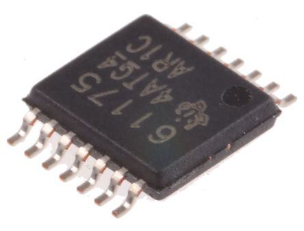
| 描述 | IC REG MULTI CONFIG ADJ 14HTSSOP稳压器—开关式稳压器 3A High Vltg Boost Converter |
| 产品分类 | |
| 品牌 | Texas Instruments |
| 产品手册 | |
| 产品图片 |
|
| rohs | 符合RoHS无铅 / 符合限制有害物质指令(RoHS)规范要求 |
| 产品系列 | 电源管理 IC,稳压器—开关式稳压器,Texas Instruments TPS61175PWP- |
| 数据手册 | |
| 产品型号 | TPS61175PWP |
| PWM类型 | 电流模式 |
| 产品目录页面 | |
| 产品种类 | 稳压器—开关式稳压器 |
| 供应商器件封装 | 14-HTSSOP |
| 其它名称 | 296-27016-5 |
| 包装 | 管件 |
| 单位重量 | 58 mg |
| 参考设计库 | http://www.digikey.com/rdl/4294959904/4294959903/453 |
| 同步整流器 | 是 |
| 商标 | Texas Instruments |
| 安装类型 | 表面贴装 |
| 安装风格 | SMD/SMT |
| 封装 | Tube |
| 封装/外壳 | 14-TSSOP (0.173",4.40mm 宽)裸焊盘 |
| 封装/箱体 | HTSSOP-14 |
| 工作温度 | -40°C ~ 85°C |
| 工作温度范围 | - 40 C to + 85 C |
| 工厂包装数量 | 90 |
| 开关频率 | 2.2 MHz |
| 拓扑结构 | Boost |
| 最大工作温度 | + 85 C |
| 最大输入电压 | 18 V |
| 最小工作温度 | - 40 C |
| 最小输入电压 | 2.9 V |
| 标准包装 | 90 |
| 特色产品 | http://www.digikey.com/cn/zh/ph/texas-instruments/tps61175.html |
| 电压-输入 | 2.9 V ~ 18 V |
| 电压-输出 | 2.9 V ~ 38 V |
| 电流-输出 | 3A |
| 类型 | 升压(升压),回扫,Sepic |
| 系列 | TPS61175 |
| 设计资源 | http://www.digikey.com/product-highlights/cn/zh/texas-instruments-webench-design-center/3176 |
| 输入电压 | 2.9 V to 18 V |
| 输出数 | 1 |
| 输出电压 | 2.9 V to 38 V |
| 输出电流 | 3 A |
| 输出端数量 | 1 Output |
| 输出类型 | 可调式 |
| 配用 | /product-detail/zh/TPS61175EVM-326/296-29315-ND/2232829/product-detail/zh/TPS61175EVM-588/296-31231-ND/2353731 |
| 频率-开关 | 210kHz ~ 2.2MHz |


- 商务部:美国ITC正式对集成电路等产品启动337调查
- 曝三星4nm工艺存在良率问题 高通将骁龙8 Gen1或转产台积电
- 太阳诱电将投资9.5亿元在常州建新厂生产MLCC 预计2023年完工
- 英特尔发布欧洲新工厂建设计划 深化IDM 2.0 战略
- 台积电先进制程称霸业界 有大客户加持明年业绩稳了
- 达到5530亿美元!SIA预计今年全球半导体销售额将创下新高
- 英特尔拟将自动驾驶子公司Mobileye上市 估值或超500亿美元
- 三星加码芯片和SET,合并消费电子和移动部门,撤换高东真等 CEO
- 三星电子宣布重大人事变动 还合并消费电子和移动部门
- 海关总署:前11个月进口集成电路产品价值2.52万亿元 增长14.8%


PDF Datasheet 数据手册内容提取
Product Order Technical Tools & Support & Folder Now Documents Software Community TPS61175 SLVS892F–DECEMBER2008–REVISEDAPRIL2019 TPS61175 3-A High-Voltage Boost Converter With Soft Start and Programmable Switching Frequency 1 Features 3 Description • 2.9-Vto18-VInputvoltagerange The TPS61175 device is a monolithic switching 1 regulator with integrated 3-A, 40-V power switch. The • 3-A,40-VInternalswitch device can be configured in several standard • High-efficiencypowerconversion:Upto93% switching-regulator topologies, including boost, • Frequencysetbyexternalresistor:200kHzto2.2 SEPIC, and flyback. The device has a wide input MHz voltagerangetosupportapplicationwithinputvoltage from multicell batteries or regulated 5-V, 12-V power • Synchronousexternalswitchingfrequency rails. • User-definedsoftstartintofullload The TPS61175 regulates the output voltage with • Skip-switchingcycleforoutputregulationatlight current mode pulse width modulation (PWM) control. load The switching frequency of PWM is set by either an • 14-PinHTSSOPpackagewith PowerPad™ external resistor or an external clock signal. The user • CreateacustomdesignusingtheTPS61175with can program the switching frequency from 200 kHz to 2.2MHz. theWEBENCHPowerDesigner The device features a programmable soft-start 2 Applications function to limit inrush current during start-up, and has other built-in protection features, such as pulse- • 5-Vto12-V,24-VPowerconversion by-pulse overcurrent limit and thermal shutdown. The • SupportsSEPICandflybacktopologies TPS61175 is available in 14-pin HTSSOP package • ADSLmodems withPowerPad. • TVtuners DeviceInformation(1) PARTNUMBER PACKAGE BODYSIZE(NOM) TPS61175 HTSSOP(14) 5.00mm×4.40mm (1) For all available packages, see the orderable addendum at theendofthedatasheet. SimplifiedSchematic VIN L1 D1 VOUT C1 C2 TPS61175 R1 VIN SW EN SW FREQ FB SS PGND COMP PGND R2 Syn PGND R4 C3 R3 AGND NC C4 Copyright©2016,TexasInstrumentsIncorporated 1 An IMPORTANT NOTICE at the end of this data sheet addresses availability, warranty, changes, use in safety-critical applications, intellectualpropertymattersandotherimportantdisclaimers.PRODUCTIONDATA.
TPS61175 SLVS892F–DECEMBER2008–REVISEDAPRIL2019 www.ti.com Table of Contents 1 Features.................................................................. 1 8 ApplicationandImplementation........................ 12 2 Applications........................................................... 1 8.1 ApplicationInformation............................................12 3 Description............................................................. 1 8.2 TypicalApplication .................................................12 4 RevisionHistory..................................................... 2 9 PowerSupplyRecommendations...................... 20 5 PinConfigurationandFunctions......................... 3 10 Layout................................................................... 20 6 Specifications......................................................... 4 10.1 LayoutGuidelines.................................................20 6.1 AbsoluteMaximumRatings .....................................4 10.2 LayoutExample....................................................20 6.2 ESDRatings..............................................................4 10.3 ThermalConsiderations........................................21 6.3 RecommendedOperatingConditions.......................4 11 DeviceandDocumentationSupport................. 22 6.4 ThermalInformation..................................................5 11.1 DeviceSupport......................................................22 6.5 ElectricalCharacteristics...........................................5 11.2 DevelopmentSupport...........................................22 6.6 TypicalCharacteristics..............................................6 11.3 ReceivingNotificationofDocumentationUpdates22 7 DetailedDescription.............................................. 8 11.4 CommunityResources..........................................22 7.1 Overview...................................................................8 11.5 Trademarks...........................................................22 7.2 FunctionalBlockDiagram.........................................8 11.6 ElectrostaticDischargeCaution............................22 7.3 FeatureDescription...................................................9 11.7 Glossary................................................................23 7.4 DeviceFunctionalModes........................................11 12 Mechanical,Packaging,andOrderable Information........................................................... 23 4 Revision History ChangesfromRevisionE(February2019)toRevisionF Page • ChangedSoftStartfigurereferencetopointtothecorrectsoftstartwaveform. .................................................................. 9 • Changed"≤"signinEquation7to"≥".................................................................................................................................. 14 ChangesfromRevisionD(April2016)toRevisionE Page • ChangedHandingRatingstabletoESDRatings;movedStorageTemperaturetoAbsoluteMaximumRatings ................ 4 • UpdatedsymbolsinThermalInformation.............................................................................................................................. 5 • AddedtheI fortheI calculationequation......................................................................................................... 14 IN(MAX) OUT(max) ChangesfromRevisionC(August2014)toRevisionD Page • RevisedsecondparagraphofMinimumONTimeandPulseSkippingsectionorclarity.................................................... 11 ChangesfromRevisionB(February2012)toRevisionC Page • AddedHandlingRatingtable,FeatureDescriptionsection,DeviceFunctionalModes,Applicationand Implementationsection,PowerSupplyRecommendationssection,Layoutsection,DeviceandDocumentation Supportsection,andMechanical,Packaging,andOrderableInformationsection................................................................ 1 ChangesfromRevisionA(October2010)toRevisionB Page • ReplacedtheDissipationRatingsTablewiththeThermalInformationTable........................................................................ 4 ChangesfromOriginal(December2008)toRevisionA Page • ChangedtheOrderingInformationtable-PartNumberFrom:TPS61175To:TPS61175PWP;Removedthe PackageMarkingcolumn ...................................................................................................................................................... 1 2 SubmitDocumentationFeedback Copyright©2008–2019,TexasInstrumentsIncorporated ProductFolderLinks:TPS61175
TPS61175 www.ti.com SLVS892F–DECEMBER2008–REVISEDAPRIL2019 5 Pin Configuration and Functions TSSOP 14Pins TopView SW 1 14 PGND SW 2 13 PGND VIN 3 12 PGND EN 4 11 NC SS 5 10 FREQ SYNC 6 9 FB AGND 7 8 COMP PinFunctions PIN DESCRIPTION I/O NAME NO. AGND 7 I SignalgroundoftheIC COMP 8 O Outputoftheinternaltransconductanceerroramplifier.AnexternalRCnetworkisconnectedtothispinto compensatetheregulator. EN 4 I Enablepin.Whenthevoltageofthispinfallsbelowtheenablethresholdformorethan10ms,theICturns off. FB 9 I Feedbackpinforpositivevoltageregulation.Connecttothecentertapofaresistordividertoprogramthe outputvoltage. FREQ 10 O Switchfrequencyprogrampin.Anexternalresistorisconnectedtothispintosetswitchfrequency.See applicationsectionforinformationonhowtosizetheFREQresistor. NC 11 I Reservedpin.Mustconnectthispintoground. PGND 12,13,14 I PowergroundoftheIC.ItisconnectedtothesourceofthePWMswitch. SS 5 O Softstartprogrammingpin.AcapacitorbetweentheSSpinandGNDpinprogramssoftstarttiming.See ApplicationandImplementationforinformationonhowtosizetheSScapacitor. SW 1,2 I ThisistheswitchingnodeoftheIC.ConnectSWtotheswitchedsideoftheinductor. SYNC 6 I Switchfrequencysynchronouspin.CustomerscanuseanexternalsignaltosettheICswitchfrequency between200-kHzand2.2-MHz.Ifnotused,thispinshouldbetiedtoAGNDasshortaspossibletoavoid noisecoupling. ThermalPad Thethermalpadshouldbesolderedtotheanalogground.Ifpossible,usethermalviatoconnecttotopand internalgroundplanelayersforidealpowerdissipation. VIN 3 I TheinputsupplypinfortheIC.ConnectVINtoasupplyvoltagebetween2.9Vand18V.Itisacceptable forthevoltageonthepintobedifferentfromtheboostpowerstageinputforapplicationsrequiringvoltage beyondVINrange. Copyright©2008–2019,TexasInstrumentsIncorporated SubmitDocumentationFeedback 3 ProductFolderLinks:TPS61175
TPS61175 SLVS892F–DECEMBER2008–REVISEDAPRIL2019 www.ti.com 6 Specifications 6.1 Absolute Maximum Ratings overoperatingfree-airtemperaturerange(unlessotherwisenoted)(1) MIN MAX UNIT SupplyvoltagesonpinVIN(2) –0.3 20 V VoltagesonpinsEN(2) –0.3 20 V VoltageonpinFB,FREQandCOMP(2) –0.3 3 V VoltageonpinSYNC,SS(2) –0.3 7 V VoltageonpinSW(2) –0.3 40 V Continuouspowerdissipation SeeThermalInformation Operatingjunctiontemperaturerange –40 150 °C Storagetemperature,T –65 150 °C stg (1) Stressesbeyondthoselistedunderabsolutemaximumratingsmaycausepermanentdamagetothedevice.Thesearestressratings onlyandfunctionaloperationofthedeviceattheseoranyotherconditionsbeyondthoseindicatedunderrecommendedoperating conditionsisnotimplied.Exposuretoabsolute-maximum-ratedconditionsforextendedperiodsmayaffectdevicereliability. (2) Allvoltagevaluesarewithrespecttonetworkgroundterminal. 6.2 ESD Ratings VALUE UNIT Human-bodymodel(HBM),perANSI/ESDA/JEDECJS-001(1) ±2000 V(ESD) Electrostaticdischarge Charged-devicemodel(CDM),perJEDECspecificationJESD22- V C101(2) ±500 (1) JEDECdocumentJEP155statesthat500-VHBMallowssafemanufacturingwithastandardESDcontrolprocess. (2) JEDECdocumentJEP157statesthat250-VCDMallowssafemanufacturingwithastandardESDcontrolprocess. 6.3 Recommended Operating Conditions overoperatingfree-airtemperaturerange(unlessotherwisenoted) MIN NOM MAX UNIT V Inputvoltage 2.9 18 V IN V Outputvoltage V 38 V O IN L Inductor(1) 4.7 47 μH f Switchingfrequency 200 2200 kHz SW C Inputcapacitor 4.7 μF I C Outputcapacitor 4.7 μF O V Externalswitchingfrequencylogic 5 V SYN T Operatingambienttemperature –40 85 °C A T Operatingjunctiontemperature –40 125 °C J (1) Theinductancevaluedependsontheswitchingfrequencyandendapplication.Whilelargervaluesmaybeused,valuesbetween4.7- μHand47-μHhavebeensuccessfullytestedinvariousapplications.RefertoSelectingtheInductorfordetail. 4 SubmitDocumentationFeedback Copyright©2008–2019,TexasInstrumentsIncorporated ProductFolderLinks:TPS61175
TPS61175 www.ti.com SLVS892F–DECEMBER2008–REVISEDAPRIL2019 6.4 Thermal Information TPS61175 THERMALMETRIC(1) PWP(HTSSOP) UNIT 14PINS R Junction-to-ambientthermalresistance 45.2 °C/W θJA R Junction-to-case(top)thermalresistance 34.9 °C/W θJC(top) R Junction-to-boardthermalresistance 30.1 °C/W θJB ψ Junction-to-topcharacterizationparameter 1.5 °C/W JT ψ Junction-to-boardcharacterizationparameter 29.9 °C/W JB R Junction-to-case(bottom)thermalresistance 5.8 °C/W θJC(bot) (1) Formoreinformationabouttraditionalandnewthermalmetrics,seetheSemiconductorandICPackageThermalMetricsapplication report(SPRA953). 6.5 Electrical Characteristics FSW=1.2MHz(R =80kΩ),V =3.6V,T =–40°Cto+85°C,typicalvaluesareatT =25°C(unlessotherwisenoted) freq IN A A PARAMETER TESTCONDITIONS MIN TYP MAX UNIT SUPPLYCURRENT V Inputvoltagerange 2.9 18 V IN I OperatingquiescentcurrentintoVin DevicePWMswitchingwithoutload 3.5 mA Q I Shutdowncurrent EN=GND 1.5 μA SD V Under-voltagelockoutthreshold 2.5 2.7 V UVLO V Under-voltagelockouthysteresis 130 mV hys ENABLEANDREFERENCECONTROL V ENlogichighvoltage V =2.9Vto18V 1.2 V enh IN V ENlogiclowvoltage V =2.9Vto18V 0.4 V enl IN V SYNlogichighvoltage 1.2 SYNh V SYNlogiclowvoltage 0.4 V SYNl R ENpulldownresistor 400 800 1600 kΩ en T Shutdowndelay,SSdischarge ENhightolow 10 ms off VOLTAGEANDCURRENTCONTROL V Voltagefeedbackregulationvoltage 1.204 1.229 1.254 V REF I Voltagefeedbackinputbiascurrent 200 nA FB I Comppinsinkcurrent V =V +200mV,V =1V 50 μA sink FB REF COMP I Comppinsourcecurrent V =V –200mV,V =1V 130 μA source FB REF COMP V Comppinclampvoltage HighClamp,V =1V 3 V CCLP FB LowClamp,V =1.5V 0.75 FB V Comppinthreshold Dutycycle=0% 0.95 V CTH G Erroramplifiertransconductance 240 340 440 μmho ea R Erroramplifieroutputresistance 10 MΩ ea f Erroramplifiercrossoverfrequency 500 KHz ea Copyright©2008–2019,TexasInstrumentsIncorporated SubmitDocumentationFeedback 5 ProductFolderLinks:TPS61175
TPS61175 SLVS892F–DECEMBER2008–REVISEDAPRIL2019 www.ti.com Electrical Characteristics (continued) FSW=1.2MHz(R =80kΩ),V =3.6V,T =–40°Cto+85°C,typicalvaluesareatT =25°C(unlessotherwisenoted) freq IN A A PARAMETER TESTCONDITIONS MIN TYP MAX UNIT FREQUENCY Rfreq=480kΩ 0.16 0.21 0.26 f Oscillatorfrequency Rfreq=80kΩ 1.0 1.2 1.4 MHz S Rfreq=40kΩ 1.76 2.2 2.64 D Maximumdutycycle V =1V,Rfreq=80kΩ 89% 93% max FB V FREQpinvoltage 1.229 V FREQ T Minimumonpulsewidth Rfreq=80kΩ 60 ns min_on POWERSWITCH R N-channelMOSFETon-resistance V =V =3.6V 0.13 0.25 Ω DS(ON) IN GS V =V =3.0V 0.13 0.3 IN GS I N-channelleakagecurrent V =40V,T =25°C 1 μA LN_NFET DS A OC,OVPANDSS I N-ChannelMOSFETcurrentlimit D=D 3 3.8 5 A LIM max I Softstartbiascurrent Vss=0V 6 μA SS THERMALSHUTDOWN T Thermalshutdownthreshold 160 °C shutdown T Thermalshutdownthresholdhysteresis 15 °C hysteresis 6.6 Typical Characteristics CircuitofFigure1;L1=D104C2-10μH;D1=SS3P6L-E3/86A,R4=80kΩ,R3=10kΩ,C4=22nF, C2=10μF;V =5V,V =24V,I =200mA(unlessotherwisenoted) IN OUT OUT Table1.TableOfGraphs FIGURE Efficiency V =5V,V =12V,24V,35V Figure1 IN OUT Efficiency V =5V,12V;V =24V Figure2 IN OUT Erroramplifier vsTemperature Figure3 transconductance Switchcurrentlimit vsTemperature Figure4 Switchcurrentlimit vsDutycycle Figure5 FBaccuracy vsTemperature Figure6 Linetransientresponse VIN=4.5Vto5V Figure12 Loadtransientresponse IOUT=100mAto300mA;referto'compensatingthecontrolloop'foroptimization Figure13 PWMOperation Figure14 Pulseskipping Noload Figure15 Start-up C3=47nF Figure16 6 SubmitDocumentationFeedback Copyright©2008–2019,TexasInstrumentsIncorporated ProductFolderLinks:TPS61175
TPS61175 www.ti.com SLVS892F–DECEMBER2008–REVISEDAPRIL2019 100 100 VI= 5 V 90 VO= 12 V 90 VI= 12 V VO= 24 V VI= 5 V % 80 % 80 ncy - ncy - cie VO= 35 V cie Effi 70 Effi 70 60 60 VO= 24 V 50 50 0 0.2 0.4 0.6 0.8 1 1.2 0 0.2 0.4 0.6 0.8 1 1.2 IO- Output Current -A IO- Output Current -A Figure1.EfficiencyvsOutputCurrent Figure2.EfficiencyvsOutputCurrent 400 5 os 380 4.5 h m A ce - mit - an Li onduct 360 urrent 4 Transc Overc A 340 3.5 E 320 3 -40 -20 0 20 40 60 80 100 120 0.2 0.4 0.6 0.8 1 TA- Free-Air Temperature - °C Duty Cycle - % Figure3.ErrorAmplifierTransconductancevsFree-Air Figure4.OvercurrentLimitvsDutyCycle Temperature 4 1240 3.9 1235 A mit - 3.8 mV vercurrent Li 3.7 FB Voltage - 1230 O 1225 3.6 3.5 1220 -40 -20 0 20 40 60 80 100 120 -40 -20 0 20 40 60 80 100 120 TA- Free-Air Temperature - °C TA- Free-Air Temperature - °C Figure5.OvercurrentLimitvsFree-AirTemperature Figure6.FBVoltagevsFree-AirTemperature Copyright©2008–2019,TexasInstrumentsIncorporated SubmitDocumentationFeedback 7 ProductFolderLinks:TPS61175
TPS61175 SLVS892F–DECEMBER2008–REVISEDAPRIL2019 www.ti.com 7 Detailed Description 7.1 Overview The TPS61175 integrates a 40-V low-side switch FET for up to 38-V output. The device regulates the output with current mode pulse width modulation (PWM) control. The PWM control circuitry turns on the switch at the beginning of each switching cycle. The input voltage is applied across the inductor and stores the energy as inductor current ramps up. During this portion of the switching cycle, the load current is provided by the output capacitor. When the inductor current rises to the threshold set by the error amplifier output, the power switch turns off and the external Schottky diode is forward biased. The inductor transfers stored energy to replenish the output capacitor and supply the load current. This operation repeats each every switching cycle. As shown in Functional Block Diagram, the duty cycle of the converter is determined by the PWM control comparator which compares the error amplifier output and the current signal. The switching frequency is programmed by the externalresistororsynchronizedtoanexternalclocksignal. A ramp signal from the oscillator is added to the current ramp to provide slope compensation. Slope compensation is necessary to avoid subharmonic oscillation that is intrinsic to the current mode control at duty cyclehigherthan50%.Iftheinductorvalueislowerthan4.7 μH,theslopecompensationmaynotbeadequate. The feedback loop regulates the FB pin to a reference voltage through a transconductance error amplifier. The output of the error amplifier is connected to the COMP pin. An external RC compensation network is connected totheCOMPpintooptimizethefeedbackloopforstabilityandtransientresponse. 7.2 Functional Block Diagram L1 D1 C1 C2 R1 FB VIN SW R2 FB EA EN Gate 1.229 V Driver Reference COMP R3 PWM Control C4 Ramp Current + Generator Sensor Oscillator SS FREQ SYNC AGND PGND C3 R4 Copyright©2016,TexasInstrumentsIncorporated 8 SubmitDocumentationFeedback Copyright©2008–2019,TexasInstrumentsIncorporated ProductFolderLinks:TPS61175
TPS61175 www.ti.com SLVS892F–DECEMBER2008–REVISEDAPRIL2019 7.3 Feature Description 7.3.1 SwitchingFrequency Theswitchfrequency is set by a resistor (R4) connected to the FREQ pin of the TPS61175. Do not leave this pin open. A resistor must always be connected for proper operation. See Table 2 and Figure 7 for resistor values andcorrespondingfrequencies. Table2.SwitchingFrequencyvsExternalResistor R4(kΩ) f (kHz) SW 443 240 256 400 176 600 80 1200 51 2000 3500 3000 2500 Hz k y - 2000 c n e u q 1500 e Fr f - 1000 500 0 10 100 1000 External Resistor - kW Figure7. SwitchingFrequencyvsExternalResistor Alternatively, the TPS61175 switching frequency will synchronize to an external clock signal that is applied to the SYNC pin. The logic level of the external clock is shown in the specification table. The duty cycle of the clock is recommended in the range of 10% to 90%. The resistor also must be connected to the FREQ pin when IC is switching by the external clock. The external clock frequency must be within ±20% of the corresponding frequency set by the resistor. For example, if the corresponding frequency as set by a resistor on the FREQ pin is1.2-MHz,theexternalclocksignalshouldbeintherangeof0.96MHzto1.44MHz. If the external clock signal is higher than the frequency per the resistor on the FREQ pin, the maximum duty cycle specification (D ) should be lowered by 2%. For instance, if the resistor set value is 2.5 MHz, and the MAX externalclockis3MHz,D is87%insteadof89%. MAX 7.3.2 SoftStart The TPS61175 has a built-in soft start circuit which significantly reduces the start-up current spike and output voltage overshoot. When the IC is enabled, an internal bias current (6 μA typically) charges a capacitor (C3) on the SS pin. The voltage at the capacitor clamps the output of the internal error amplifier that determines the duty cycle of PWM control, thereby the input inrush current is eliminated. Once the capacitor reaches 1.8 V, the soft start cycle is completed and the soft-start voltage no longer clamps the error amplifier output. Refer to Figure 16 for the soft start waveform. See Table 3 for C3 and corresponding soft start time. A 47-nF capacitor eliminates theoutputovershootandreducesthepeakinductorcurrentformostapplications. Copyright©2008–2019,TexasInstrumentsIncorporated SubmitDocumentationFeedback 9 ProductFolderLinks:TPS61175
TPS61175 SLVS892F–DECEMBER2008–REVISEDAPRIL2019 www.ti.com Table3.Soft-StartTimevsC3 V (V) V (V) LOAD(A) C (μF) f (MHz) C3(nF) t (ms) OVERSHOT(mV) IN OUT OUT SW SS 47 4 none 5 24 0.4 10 1.2 10 0.8 210 100 6.5 none 12 35 0.6 10 2 10 0.4 300 When the EN is pulled low for 10 ms, the IC enters shutdown and the SS capacitor discharges through a 5-kΩ resistorforthenextsoftstart. 7.3.3 OvercurrentProtection The TPS61175 has a cycle-by-cycle overcurrent limit protection that turns off the power switch once the inductor current reaches the overcurrent limit threshold. The PWM circuitry resets itself at the beginning of the next switch cycle. During an overcurrent event, the output voltage begins to droop as a function of the load on the output. When the FB voltage drops lower than 0.9 V, the switching frequency is automatically reduced to 1/4 of the set value. The switching frequency does not reset until the overcurrent condition is removed. This feature is disabled duringsoftstart. 7.3.4 EnableandThermalShutdown The TPS61175 enters shutdown when the EN voltage is less than 0.4 V for more than 10 ms. In shutdown, the input supply current for the device is less than 1.5 μA (maximum). The EN pin has an internal 800-kΩ pulldown resistortodisablethedevicewhenitisfloating. An internal thermal shutdown turns off the device when the typical junction temperature of 160°C is exceeded. TheICrestartswhenthejunctiontemperaturedropsby15°C. 7.3.5 UndervoltageLockout(UVLO) An undervoltage lockout circuit prevents mis-operation of the device at input voltages below 2.5-V (typical). When the input voltage is below the undervoltage threshold, the device remains off, and the internal switch FET is turned off. The UVLO threshold is set below minimum operating voltage of 2.9 V to avoid any transient VIN dip triggering the UVLO and causing the device to reset. For the input voltages between UVLO threshold and 2.9 V, thedeviceattemptstooperate,butthespecificationsarenotensured. 10 SubmitDocumentationFeedback Copyright©2008–2019,TexasInstrumentsIncorporated ProductFolderLinks:TPS61175
TPS61175 www.ti.com SLVS892F–DECEMBER2008–REVISEDAPRIL2019 7.4 Device Functional Modes 7.4.1 MinimumONTimeandPulseSkipping Once the PWM switch is turned on, the TPS61175 has minimum ON pulse width of 60 ns. This sets the limit of theminimumdutycycleof the PWM switch, and it is independent of the set switching frequency. When operating conditions result in the TPS61175 having a minimum ON pulse width less than 60 ns, the IC enters pulse- skipping mode. In this mode, the device keeps the power switch off for several switching cycles to keep the output voltage from rising above the regulated voltage. This operation typically occurs in light load condition when the PWM operates in discontinuous mode. Pulse skipping increases the output voltage ripple, see Figure15. When setting switching frequency higher than 1.2 MHz, TI recommends using an external synchronous clock as switching frequency to ensure pulse-skipping function works at light load. When using the internal switching frequency above 1.2 MHz, the pulse-skipping operation may not function. When the pulse-skipping function does not work at light load, the TPS61175 always runs in PWM mode with minimum ON pulse width. To keep the output voltage in regulation, a minimum load is required. The minimum load is related to the input voltage, output voltage, switching frequency, external inductor value and the maximum value of the minimum ON pulse width. Use Equation 1 and Equation 2 to calculate the required minimum load at the worst case. The maximum t min_ON could be estimated to 80 ns. C is the total parasite capacitance at the switching node SW pin. It could be SW estimatedto100pF. ( )2 V xt +(V +V -V )x LxC x ¦ 1 IN min_ON OUT D IN SW SW I = x WhenV +V -V <V (min_load) 2 Lx (V +V -V ) OUT D IN IN OUT D IN (1) ( )2 V xt +V x LxC x ¦ 1 IN min_ON IN SW SW I = x WhenV +V -V >V (min_load) 2 Lx (V +V -V ) OUT D IN IN OUT D IN (2) Copyright©2008–2019,TexasInstrumentsIncorporated SubmitDocumentationFeedback 11 ProductFolderLinks:TPS61175
TPS61175 SLVS892F–DECEMBER2008–REVISEDAPRIL2019 www.ti.com 8 Application and Implementation 8.1 Application Information The following section provides a step-by-step design approach for configuring the TPS61175 as a voltage regulating boost converter, as shown in Figure 8. When configured as SEPIC or flyback converter, a different designapproachisrequired. 8.2 Typical Application VIN L1 D1 VOUT C1 C2 TPS61175 VIN SW R1 EN SW FREQ FB SS PGND COMP PGND R2 R4 C3 R3 Syn PGND AGND NC C4 Copyright©2016,TexasInstrumentsIncorporated Figure8. BoostConverterConfiguration 8.2.1 DesignRequirements Table4.DesignParameters PARAMETERS VALUES Inputvoltage 5V Outputvoltage 24V Operatingfrequency 1.2MHz 8.2.2 DetailedDesignProcedure 8.2.2.1 CustomDesignwithWEBENCHTools ClickheretocreateacustomdesignusingtheTPS61175devicewiththe WEBENCH® PowerDesigner. 1. StartbyenteringyourV ,V andI requirements. IN OUT OUT 2. Optimize your design for key parameters like efficiency, footprint and cost using the optimizer dial and comparethisdesignwithotherpossiblesolutionsfromTexasInstruments. 3. WEBENCH Power Designer provides you with a customized schematic along with a list of materials with real timepricingandcomponentavailability. 4. Inmostcases,youwillalsobeableto: – Runelectricalsimulationstoseeimportantwaveformsandcircuitperformance, – Runthermalsimulationstounderstandthethermalperformanceofyourboard, – ExportyourcustomizedschematicandlayoutintopopularCADformats, – PrintPDFreportsforthedesign,andshareyourdesignwithcolleagues. 5. GetmoreinformationaboutWEBENCHtoolsatwww.ti.com/webench. 12 SubmitDocumentationFeedback Copyright©2008–2019,TexasInstrumentsIncorporated ProductFolderLinks:TPS61175
TPS61175 www.ti.com SLVS892F–DECEMBER2008–REVISEDAPRIL2019 8.2.2.2 DeterminingtheDutyCycle The TPS61175 has a maximum worst case duty cycle of 89% and a minimum on time of 60 ns. These two constraints place limitations on the operating frequency that can be used for a given input to output conversion ratio.Thedutycycleatwhichtheconverteroperatesisdependentonthemode in which the converter is running. If the converter is running in discontinuous conduction mode (DCM), where the inductor current ramps to zero at the end of each cycle, the duty cycle varies with changes to the load much more than it does when running in continuous conduction mode (CCM). In continuous conduction mode, where the inductor maintains a dc current, thedutycycleisrelatedprimarilytotheinputandoutputvoltagesascomputedinEquation3: V +V - V D = OUT D IN V +V OUT D (3) In discontinuous mode the duty cycle is a function of the load, input and output voltages, inductance and switchingfrequencyascomputedinEquation4: 2 ´ (V +V ) ´ I ´ L ´ ¦ D= OUT D OUT SW V 2 IN (4) All converters using a diode as the freewheeling or catch component have a load current level at which they transition from discontinuous conduction to continuous conduction. This is the point where the inductor current just falls to zero. At higher load currents, the inductor current does not fall to zero but remains flowing in a positive direction and assumes a trapezoidal wave shape as opposed to a triangular wave shape. This load boundary between discontinuous conduction and continuous conduction can be found for a set of converter parametersinEquation5: 2 (V +V - V ) ´ V OUT D IN IN I = OUT(crit) 2 2 ´ (V +V ) ´ ¦ ´ L OUT D SW (5) For loads higher than the result of Equation 5, the duty cycle is given by Equation 3 and for loads less that the results of Equation 4, the duty cycle is given Equation 5. For Equation 3 through Equation 5, the variable definitionsareasfollows: • V istheoutputvoltageoftheconverterinV OUT • V istheforwardconductionvoltagedropacrosstherectifierorcatchdiodeinV D • V istheinputvoltagetotheconverterinV IN • I istheoutputcurrentoftheconverterinA OUT • ListheinductorvalueinH • f istheswitchingfrequencyinHz SW Unless otherwise stated, the design equations that follow assume that the converter is running in continuous mode. 8.2.2.3 SelectingtheInductor Theselection of the inductor affects steady state operation as well as transient behavior and loop stability. These factors make it the most important component in power regulator design. There are three important inductor specifications, inductor value, DC resistance and saturation current. Considering inductor value alone is not enough. Inductor values can have ±20% tolerance with no current bias. When the inductor current approaches saturation level, its inductance can fall to some percentage of its 0-A value depending on how the inductor vendor defines saturation current. For CCM operation, the rule of thumb is to choose the inductor so that its inductor ripple current(ΔI )isnomorethanacertainpercentage(RPL%=20–40%)ofitsaverageDCvalue(I =I ). L IN(AVG) L(AVG) V ´ D (V + V - V ) ´ (1 - D) 1 DI = IN = OUT D IN = L L ´ ¦SW L ´ ¦SW é æ 1 1 öù êL´¦ ´ç + ÷ú êë SW èVOUT +VD - VIN VIN øúû P £RPL% ´ OUT V ´ η IN est (6) Copyright©2008–2019,TexasInstrumentsIncorporated SubmitDocumentationFeedback 13 ProductFolderLinks:TPS61175
TPS61175 SLVS892F–DECEMBER2008–REVISEDAPRIL2019 www.ti.com RearrangingandsolvingforLgives: η ´ V L ³ est IN é æ 1 1 öù êêë¦SW çèVOUT + VD - VIN +VIN ÷øúúû ´ RPL% POUT (7) Choosing the inductor ripple current to closer to 20% of the average inductor current results in a larger inductance value, maximizes the converter’s potential output current and minimizes EMI. Choosing the inductor ripple current closer to 40% of I results in a smaller inductance value, and a physically smaller inductor, L(AVG) improves transient response but results in potentially higher EMI and lower efficiency if the DCR of the smaller packaged inductor is significantly higher. Using an inductor with a smaller inductance value than computed above may result in the converter operating in DCM. This reduces the maximum output current of the boost converter, causes larger input voltage and output ripple, and typically reduces efficiency. Table 5 lists the recommendedinductorfortheTPS61175. Table5.RecommendedInductorsforTPS61175 L DCRMAX SATURATIONCURRENT SIZE PARTNUMBER VENDOR (μH) (mΩ) (A) (L×W×Hmm) D104C2 10 44 3.6 10.4×10.4×4.8 TOKO VLF10040 15 42 3.1 10×9.7×4 TDK CDRH105RNP 22 61 2.9 10.5×10.3×5.1 Sumida MSS1038 15 50 3.8 10×10.2×3.8 Coilcraft The device has built-in slope compensation to avoid subharmonic oscillation associated with current mode control. If the inductor value is lower than 4.7 μH, the slope compensation may not be adequate, and the loop can be unstable. Applications requiring inductors above 47 μH have not been evaluated. Therefore, the user is responsible for verifying operation if they select an inductor that is outside the 4.7-μH to 47-μH recommended range. 8.2.2.4 ComputingtheMaximumOutputCurrent Theover-currentlimitfortheintegratedpowerFETlimitsthemaximuminput current and thus the maximum input power for a given input voltage. Maximum output power is less than maximum input power due to power conversion losses. Therefore, the current limit setting, input voltage, output voltage and efficiency can all change the maximum current output (I ). The current limit clamps the peak inductor current, therefore the ripple OUT(MAX) hastobesubtractedtoderivemaximumDCcurrent. V u I u K V u I u(1(cid:16)%RPL/2)uK IN(max) IN(max) est IN(max) LIM est I OUT(max) V V OUT OUT where • I =overcurrentlimit LIM • η =efficiencyestimatebasedonsimilarapplicationsorcomputedabove (8) est For instance, when V = 12 V is boosted to V = 24 V, the inductor is 10 µH, the Schottky forward voltage is IN OUT 0.4 V, and the switching frequency is 1.2 MHz; then the maximum output current is 1.2 A in typical condition, assuming90%efficiencyanda%RPL=20%. 8.2.2.5 SettingOutputVoltage TosettheoutputvoltageineitherDCMorCCM,selectthevaluesofR1andR2accordingtoEquation9: æR1 ö Vout=1.229 V ´ ç + 1÷ èR2 ø æ Vout ö R1 =R2 ´ - 1 ç ÷ è1.229V ø (9) Considering the leakage current through the resistor divider and noise decoupling into FB pin, an optimum value for R2 is around 10 k. The output voltage tolerance depends on the V accuracy and the tolerance of R1 and FB R2. 14 SubmitDocumentationFeedback Copyright©2008–2019,TexasInstrumentsIncorporated ProductFolderLinks:TPS61175
TPS61175 www.ti.com SLVS892F–DECEMBER2008–REVISEDAPRIL2019 8.2.2.6 SettingtheSwitchingFrequency Choose the appropriate resistor from the resistance versus frequency table Table 2 or graph Figure 7. A resistor mustbeplacedfromtheFREQpintoground,evenifanexternaloscillationisappliedforsynchronization. Increasing switching frequency reduces the value of external capacitors and inductors, but also reduces the powerconversionefficiency.Theusershouldsetthefrequencyfortheminimumtolerableefficiency. 8.2.2.7 SettingtheSoft-StartTime Choose the appropriate capacitor from the soft-start table, Table 3. Increasing the soft-start time reduces the overshootduringstart-up. 8.2.2.8 SelectingtheSchottkyDiode The high switching frequency of the TPS61175 demands a high-speed rectification for optimum efficiency. Ensure that the diode’s average and peak current rating exceed the average output current and peak inductor current. In addition, the diode’s reverse breakdown voltage must exceed the switch FET rating voltage of 40 V. So, the VISHAY SS3P6L-E3/86A is recommended for TPS61175. The power dissipation of the diode's package mustbelargerthanI ×V . OUT(max) D 8.2.2.9 SelectingtheInputandOutputCapacitors The output capacitor is mainly selected to meet the requirements for the output ripple and load transient. Then the loop is compensated for the output capacitor selected. The output ripple voltage is related to the capacitor’s capacitance and its equivalent series resistance (ESR). Assuming a capacitor with zero ESR, the minimum capacitanceneededforagivenripplecanbecalculatedusingEquation10: ( ) V - V I OUT IN out C = out V ´ Fs ´ V OUT ripple (10) where V = peak to peak output ripple. The additional output ripple component caused by ESR is calculated ripple using: V =I×R ripple_ESR ESR Due to its low ESR, V can be neglected for ceramic capacitors, but must be considered if tantalum or ripple_ESR electrolyticcapacitorsareused. The minimum ceramic output capacitance needed to meet a load transient requirement can be estimated using Equation11: ΔI C = TRAN OUT 2 ´ p ´ f ´ ΔV LOOP-BW TRAN where • ΔI isthetransientloadcurrentstep TRAN • ΔV istheallowedvoltagedipfortheloadcurrentstep TRAN • f isthecontrolloopbandwidth(thatis,thefrequencywherethecontrolloopgaincrosseszero). (11) LOOP-BW Care must be taken when evaluating a ceramic capacitor’s derating under DC bias, aging and AC signal. For example, larger form factor capacitors (in 1206 size) have their self resonant frequencies in the range of the switching frequency. So the effective capacitance is significantly lower. The DC bias can also significantly reduce capacitance. Ceramic capacitors can loss as much as 50% of its capacitance at its rated voltage. Therefore, one mustaddmarginonthevoltageratingtoensureadequatecapacitanceattherequiredoutputvoltage. For a typical boost converter implementation, at least 4.7 μF of ceramic input and output capacitance is recommended. Additional input and output capacitance may be required to meet ripple and/or transient requirements. Thepopularvendorsforhighvalueceramiccapacitorsare: TDK(http://www.component.tdk.com/components.php) Murata(http://www.murata.com/cap/index.html) Copyright©2008–2019,TexasInstrumentsIncorporated SubmitDocumentationFeedback 15 ProductFolderLinks:TPS61175
TPS61175 SLVS892F–DECEMBER2008–REVISEDAPRIL2019 www.ti.com 8.2.2.10 CompensatingtheSmallSignalControlLoop All continuous mode boost converters have a right half plane zero (ƒ ) due to the inductor being removed RHPZ from the output during charging. In a traditional voltage mode controlled boost converter, the inductor and output capacitor form a small signal double pole. For a negative feedback system to be stable, the fed back signal must have a gain less than 1 before having 180 degrees of phase shift. With its double pole and RHPZ all providing phase shift, voltage mode boost converters are a challenge to compensate. In a converter with current mode control, there are essentially two loops, an inner current feedback loop created by the inductor current information sensed across R (40mΩ) and the output voltage feedback loop. The inner current loop allows SENSE the switch, inductor and modulator to be lumped together into a small signal variable current source controlled by theerroramplifier,asshowninFigure9. (1-D) R1 R SENSE _ + C2 RO 2 C4 Vref C5 (optional) R3 R2 RESR Figure9. SmallSignalModelofaCurrentModeBoostinCCM Thenewpowerstage,includingtheslopecompensation,smallsignalmodelbecomes: æ s öæ s ö ç1+ ÷ç1- ÷ G (s)= ROUT´(1-D)´è 2´p´¦ESR øè 2´p´¦RHPZ ø´He(s) PS 2´R s SENSE 1+ 2´p´¦ P (12) Where 2 ¦P = 2p´RO ´C2 (13) 1 ¦ » ESR 2p ´ R ´ C2 ESR (14) 2 R æ V ö ¦RHPZ = 2p O´ L ´ çèVOIUNT ÷ø (15) And 1 He(s)= éæ Seö ù s´êç1+ ÷´(1-D)-0.5ú ëè Snø û s2 1+ + ¦SW (p´¦SW)2 (16) He(s) models the inductor current sampling effect as well as the slope compensation effect on the small signal response. Note that if Sn > Se, for example, when L is smaller than recommended, the converter operates as a voltagemodeconverterandtheabovemodelnolongerholds. 16 SubmitDocumentationFeedback Copyright©2008–2019,TexasInstrumentsIncorporated ProductFolderLinks:TPS61175
TPS61175 www.ti.com SLVS892F–DECEMBER2008–REVISEDAPRIL2019 TheslopecompensationinTPS61175isshownasfollows: V +V - V Sn= OUT D IN ´ R L SENSE (17) 0.32 V/R4 0.5 mA Se= + 16´(1-D)´6pF 6 pF WhereR4isthefrequencysettingresistor (18) Figure10showsaBodeplotofatypicalCCMboostconverterpowerstage. 180 120 Gain 60 B ° d – ain− 0 hase G P –60 Phase –120 –180 fP f−Frequency−kHz Figure10. BodePlotofPowerStageGainandPhase The TPS61175 COMP pin is the output of the internal trans-conductance amplifier. Equation 19 shows the equationforfeedbackresistornetworkandtheerroramplifier. s 1+ R2 2´p´¦ H =G ´R ´ ´ Z EA EA EA R2+R1 æ s ö æ s ö ç1+ ÷´ç1+ ÷ è 2´p´¦P1ø è 2´p´¦P2 ø where • G andR aretheamplifier’strans-conductanceandoutputresistancelocatedintheElectrical EA EA Characteristicstable. (19) 1 ¦P1 = 2p´REA ´C4 (20) 1 ¦ = (optional) P2 2p´R3´C5 C5isoptionalandcanbemodeledas10pFstraycapacitance. (21) and 1 ¦ = Z 2p ´ R3 ´ C4 (22) Figure11showsatypicalbodeplotfortransferfunctionH(s). Copyright©2008–2019,TexasInstrumentsIncorporated SubmitDocumentationFeedback 17 ProductFolderLinks:TPS61175
TPS61175 SLVS892F–DECEMBER2008–REVISEDAPRIL2019 www.ti.com 180 90 Phase B ° d – Gain− Kcomp 0 Phase Gain –90 –180 <–fp1 fZ fC fp2 f−Frequency−kHz Figure11. BodePlotofFeedbackResistorsandCompensatedAmplifierGainandPhase The next step is to choose the loop crossover frequency, f . The higher in frequency that the loop gain stays C above zero before crossing over, the faster the loop response will be and therefore the lower the output voltage will droop during a step load. It is generally accepted that the loop gain cross over no higher than the lower of either 1/5 of the switching frequency, f , or 1/3 of the RHPZ frequency, f . To approximate a single pole roll- SW RHPZ offuptof ,selectR3sothatthecompensationgain,K ,atf onFigure11isthereciprocalofthegain,K , P2 COMP C PW readatfrequencyf fromtheFigure10bodeplot,ormoresimply: C K (f )=20× log(G ×R3 ×R2/(R2+R1))=1/K (f ) COMP C EA PW C This makes the total loop gain, T(s) = G (s) × H (s), zero at the f . Then, select C4 so that f ≅ f /10 and PS EA C Z C optionalf >f ×10.Followingthismethodshouldleadtoaloopwithaphasemarginnear45degrees. Lowering P2 C R3 while keeping f ≅ f /10 increases the phase margin and therefore increases the time it takes for the output Z C voltagetosettlefollowingastepload. In the TPS61175, if the FB pin voltage changes suddenly due to a load step on the output voltage, the error amplifier increases its transconductance for 8-ms in an effort to speed up the IC’s transient response and reduce output voltage droop due to the load step. For example, if the FB voltage decreases 10 mV due to load change, theerroramplifierincreasesitssourcecurrentthroughCOMPby5times;ifFBvoltageincreases11mV, the sink current through COMP is increased to 3.5 times normal value. This feature often results in saw tooth ringing on the output voltage, shown as Figure 13. Designing the loop for greater than 45 degrees of phase margin and greaterthan10-dbgainmarginminimizestheamplitudeofthisringing.Thisfeatureisdisabledduringsoftstart. 18 SubmitDocumentationFeedback Copyright©2008–2019,TexasInstrumentsIncorporated ProductFolderLinks:TPS61175
TPS61175 www.ti.com SLVS892F–DECEMBER2008–REVISEDAPRIL2019 8.2.3 ApplicationCurves VIN VOUT 1 V/div 500 mV/div AC AC VOUT 100 mV/div AC ILOAD 200 mA/div t - 200ms/div t - 100ms/div Figure12.LineTransientResponse Figure13.LoadTransientResponse VOUT SW 1 V/div 20 V/div 20 V offset VOUT 20 mV/div AC IL 500 mA/div I L 100 mA/div VOUT 100 mV/div AC t - 400 ns/div t - 400ms/div Figure14.PWMOperation Figure15.PulseSkipping EN 2 V/div VOUT 5 V/div I L 500 mA/div t - 1 ms/div Figure16.SoftStart-up Copyright©2008–2019,TexasInstrumentsIncorporated SubmitDocumentationFeedback 19 ProductFolderLinks:TPS61175
TPS61175 SLVS892F–DECEMBER2008–REVISEDAPRIL2019 www.ti.com 9 Power Supply Recommendations The device is designed to operate from an input voltage supply range between 2.9 V and 18 V. The input power supply’s output current must be rated according to the supply voltage, output voltage and output current of the TPS61175. 10 Layout 10.1 Layout Guidelines • As for all switching power supplies, especially those running at high switching frequency and high currents, layout is an important design step. If layout is not carefully done, the regulator could suffer from instability as well as noise problems. To maximize efficiency, switch rise and fall times are very fast. To prevent radiation ofhighfrequencynoise(forexample,EMI),properlayoutofthehighfrequencyswitchingpathisessential. • Minimize the length and area of all traces connected to the SW pin and always use a ground plane under the switchingregulatortominimizeinterplanecoupling. • The high current path including the switch, Schottky diode, and output capacitor, contains nanosecond rise andfalltimesandmustbekeptasshortaspossible. • The input capacitor must not only to be close to the VIN pin, but also to the GND pin in order to reduce the Iinputsupplyripple. 10.2 Layout Example VIN INPUT CAPACITOR VOUT INDUCTOR SCHOTTKY DIODE OUTPUT CAPACITOR SW SW PGND Minimizethe area of SW trace SW PGND PGND VIN PGND T he EN rm NC a lP a SS d FREQ SYNC FB AGND COMP FEEDBACK Placeenough AGND COMPENSATION VIAsaround NETWORK thermal pad to enhancethermal performance Figure17. TPS61175Layout 20 SubmitDocumentationFeedback Copyright©2008–2019,TexasInstrumentsIncorporated ProductFolderLinks:TPS61175
TPS61175 www.ti.com SLVS892F–DECEMBER2008–REVISEDAPRIL2019 10.3 Thermal Considerations Restrict the maximum IC junction temperature to 125°C under normal operating conditions. This restriction limits the power dissipation of the TPS61175. Calculate the maximum allowable dissipation, P (maximum), and keep D the actual dissipation less than or equal to P (maximum). The maximum-power-dissipation limit is determined D usingEquation23: 125°C - T P = A D(max) RqJA where • T isthemaximumambienttemperaturefortheapplication A • R isthethermalresistancejunction-to-ambientgiveninThermalInformation. (23) θJA The TPS61175 comes in a thermally enhanced TSSOP package. This package includes a thermal pad that improves the thermal capabilities of the package. The R of the TSSOP package greatly depends on the PCB θJA layout and thermal pad connection. The thermal pad must be soldered to the analog ground on the PCB. Using thermalviasunderneaththethermalpad. Copyright©2008–2019,TexasInstrumentsIncorporated SubmitDocumentationFeedback 21 ProductFolderLinks:TPS61175
TPS61175 SLVS892F–DECEMBER2008–REVISEDAPRIL2019 www.ti.com 11 Device and Documentation Support 11.1 Device Support 11.1.1 Third-PartyProductsDisclaimer TI'S PUBLICATION OF INFORMATION REGARDING THIRD-PARTY PRODUCTS OR SERVICES DOES NOT CONSTITUTE AN ENDORSEMENT REGARDING THE SUITABILITY OF SUCH PRODUCTS OR SERVICES OR A WARRANTY, REPRESENTATION OR ENDORSEMENT OF SUCH PRODUCTS OR SERVICES, EITHER ALONEORINCOMBINATIONWITHANYTIPRODUCTORSERVICE. 11.2 Development Support 11.2.1 CustomDesignwithWEBENCHTools ClickheretocreateacustomdesignusingtheTPS61175devicewiththe WEBENCH® PowerDesigner. 1. StartbyenteringyourV ,V andI requirements. IN OUT OUT 2. Optimize your design for key parameters like efficiency, footprint and cost using the optimizer dial and comparethisdesignwithotherpossiblesolutionsfromTexasInstruments. 3. WEBENCH Power Designer provides you with a customized schematic along with a list of materials with real timepricingandcomponentavailability. 4. Inmostcases,youwillalsobeableto: – Runelectricalsimulationstoseeimportantwaveformsandcircuitperformance, – Runthermalsimulationstounderstandthethermalperformanceofyourboard, – ExportyourcustomizedschematicandlayoutintopopularCADformats, – PrintPDFreportsforthedesign,andshareyourdesignwithcolleagues. 5. GetmoreinformationaboutWEBENCHtoolsatwww.ti.com/webench. 11.3 Receiving Notification of Documentation Updates To receive notification of documentation updates, navigate to the device product folder on ti.com. In the upper right corner, click on Alert me to register and receive a weekly digest of any product information that has changed.Forchangedetails,reviewtherevisionhistoryincludedinanyreviseddocument. 11.4 Community Resources The following links connect to TI community resources. Linked contents are provided "AS IS" by the respective contributors. They do not constitute TI specifications and do not necessarily reflect TI's views; see TI's Terms of Use. TIE2E™OnlineCommunity TI'sEngineer-to-Engineer(E2E)Community.Createdtofostercollaboration amongengineers.Ate2e.ti.com,youcanaskquestions,shareknowledge,exploreideasandhelp solveproblemswithfellowengineers. DesignSupport TI'sDesignSupport QuicklyfindhelpfulE2Eforumsalongwithdesignsupporttoolsand contactinformationfortechnicalsupport. 11.5 Trademarks PowerPad,E2EaretrademarksofTexasInstruments. WEBENCHisaregisteredtrademarkofTexasInstruments. Allothertrademarksarethepropertyoftheirrespectiveowners. 11.6 Electrostatic Discharge Caution Thesedeviceshavelimitedbuilt-inESDprotection.Theleadsshouldbeshortedtogetherorthedeviceplacedinconductivefoam duringstorageorhandlingtopreventelectrostaticdamagetotheMOSgates. 22 SubmitDocumentationFeedback Copyright©2008–2019,TexasInstrumentsIncorporated ProductFolderLinks:TPS61175
TPS61175 www.ti.com SLVS892F–DECEMBER2008–REVISEDAPRIL2019 11.7 Glossary SLYZ022—TIGlossary. Thisglossarylistsandexplainsterms,acronyms,anddefinitions. 12 Mechanical, Packaging, and Orderable Information The following pages include mechanical, packaging, and orderable information. This information is the most current data available for the designated devices. This data is subject to change without notice and revision of thisdocument.Forbrowser-basedversionsofthisdatasheet,refertotheleft-handnavigation. Copyright©2008–2019,TexasInstrumentsIncorporated SubmitDocumentationFeedback 23 ProductFolderLinks:TPS61175
PACKAGE OPTION ADDENDUM www.ti.com 6-Feb-2020 PACKAGING INFORMATION Orderable Device Status Package Type Package Pins Package Eco Plan Lead/Ball Finish MSL Peak Temp Op Temp (°C) Device Marking Samples (1) Drawing Qty (2) (6) (3) (4/5) TPS61175PWP ACTIVE HTSSOP PWP 14 90 Green (RoHS NIPDAU Level-2-260C-1 YEAR -40 to 85 61175 & no Sb/Br) TPS61175PWPR ACTIVE HTSSOP PWP 14 2000 Green (RoHS NIPDAU Level-2-260C-1 YEAR -40 to 85 61175 & no Sb/Br) (1) The marketing status values are defined as follows: ACTIVE: Product device recommended for new designs. LIFEBUY: TI has announced that the device will be discontinued, and a lifetime-buy period is in effect. NRND: Not recommended for new designs. Device is in production to support existing customers, but TI does not recommend using this part in a new design. PREVIEW: Device has been announced but is not in production. Samples may or may not be available. OBSOLETE: TI has discontinued the production of the device. (2) RoHS: TI defines "RoHS" to mean semiconductor products that are compliant with the current EU RoHS requirements for all 10 RoHS substances, including the requirement that RoHS substance do not exceed 0.1% by weight in homogeneous materials. Where designed to be soldered at high temperatures, "RoHS" products are suitable for use in specified lead-free processes. TI may reference these types of products as "Pb-Free". RoHS Exempt: TI defines "RoHS Exempt" to mean products that contain lead but are compliant with EU RoHS pursuant to a specific EU RoHS exemption. Green: TI defines "Green" to mean the content of Chlorine (Cl) and Bromine (Br) based flame retardants meet JS709B low halogen requirements of <=1000ppm threshold. Antimony trioxide based flame retardants must also meet the <=1000ppm threshold requirement. (3) MSL, Peak Temp. - The Moisture Sensitivity Level rating according to the JEDEC industry standard classifications, and peak solder temperature. (4) There may be additional marking, which relates to the logo, the lot trace code information, or the environmental category on the device. (5) Multiple Device Markings will be inside parentheses. Only one Device Marking contained in parentheses and separated by a "~" will appear on a device. If a line is indented then it is a continuation of the previous line and the two combined represent the entire Device Marking for that device. (6) Lead/Ball Finish - Orderable Devices may have multiple material finish options. Finish options are separated by a vertical ruled line. Lead/Ball Finish values may wrap to two lines if the finish value exceeds the maximum column width. Important Information and Disclaimer:The information provided on this page represents TI's knowledge and belief as of the date that it is provided. TI bases its knowledge and belief on information provided by third parties, and makes no representation or warranty as to the accuracy of such information. Efforts are underway to better integrate information from third parties. TI has taken and continues to take reasonable steps to provide representative and accurate information but may not have conducted destructive testing or chemical analysis on incoming materials and chemicals. TI and TI suppliers consider certain information to be proprietary, and thus CAS numbers and other limited information may not be available for release. In no event shall TI's liability arising out of such information exceed the total purchase price of the TI part(s) at issue in this document sold by TI to Customer on an annual basis. Addendum-Page 1
PACKAGE OPTION ADDENDUM www.ti.com 6-Feb-2020 OTHER QUALIFIED VERSIONS OF TPS61175 : •Automotive: TPS61175-Q1 NOTE: Qualified Version Definitions: •Automotive - Q100 devices qualified for high-reliability automotive applications targeting zero defects Addendum-Page 2
PACKAGE MATERIALS INFORMATION www.ti.com 12-Apr-2019 TAPE AND REEL INFORMATION *Alldimensionsarenominal Device Package Package Pins SPQ Reel Reel A0 B0 K0 P1 W Pin1 Type Drawing Diameter Width (mm) (mm) (mm) (mm) (mm) Quadrant (mm) W1(mm) TPS61175PWPR HTSSOP PWP 14 2000 330.0 12.4 6.9 5.6 1.6 8.0 12.0 Q1 PackMaterials-Page1
PACKAGE MATERIALS INFORMATION www.ti.com 12-Apr-2019 *Alldimensionsarenominal Device PackageType PackageDrawing Pins SPQ Length(mm) Width(mm) Height(mm) TPS61175PWPR HTSSOP PWP 14 2000 350.0 350.0 43.0 PackMaterials-Page2
None
None
None
None
None
IMPORTANTNOTICEANDDISCLAIMER TI PROVIDES TECHNICAL AND RELIABILITY DATA (INCLUDING DATASHEETS), DESIGN RESOURCES (INCLUDING REFERENCE DESIGNS), APPLICATION OR OTHER DESIGN ADVICE, WEB TOOLS, SAFETY INFORMATION, AND OTHER RESOURCES “AS IS” AND WITH ALL FAULTS, AND DISCLAIMS ALL WARRANTIES, EXPRESS AND IMPLIED, INCLUDING WITHOUT LIMITATION ANY IMPLIED WARRANTIES OF MERCHANTABILITY, FITNESS FOR A PARTICULAR PURPOSE OR NON-INFRINGEMENT OF THIRD PARTY INTELLECTUAL PROPERTY RIGHTS. These resources are intended for skilled developers designing with TI products. You are solely responsible for (1) selecting the appropriate TI products for your application, (2) designing, validating and testing your application, and (3) ensuring your application meets applicable standards, and any other safety, security, or other requirements. These resources are subject to change without notice. TI grants you permission to use these resources only for development of an application that uses the TI products described in the resource. Other reproduction and display of these resources is prohibited. No license is granted to any other TI intellectual property right or to any third party intellectual property right. TI disclaims responsibility for, and you will fully indemnify TI and its representatives against, any claims, damages, costs, losses, and liabilities arising out of your use of these resources. TI’s products are provided subject to TI’s Terms of Sale (www.ti.com/legal/termsofsale.html) or other applicable terms available either on ti.com or provided in conjunction with such TI products. TI’s provision of these resources does not expand or otherwise alter TI’s applicable warranties or warranty disclaimers for TI products. Mailing Address: Texas Instruments, Post Office Box 655303, Dallas, Texas 75265 Copyright © 2020, Texas Instruments Incorporated