ICGOO在线商城 > 集成电路(IC) > PMIC - 稳压器 - DC DC 开关稳压器 > TPS61256YFFR
 Datasheet下载
- 型号: TPS61256YFFR
- 制造商: Texas Instruments
- 库位|库存: xxxx|xxxx
- 要求:
| 数量阶梯 | 香港交货 | 国内含税 |
| +xxxx | $xxxx | ¥xxxx |
查看当月历史价格
查看今年历史价格
TPS61256YFFR产品简介:
ICGOO电子元器件商城为您提供TPS61256YFFR由Texas Instruments设计生产,在icgoo商城现货销售,并且可以通过原厂、代理商等渠道进行代购。 TPS61256YFFR价格参考¥3.17-¥7.10。Texas InstrumentsTPS61256YFFR封装/规格:PMIC - 稳压器 - DC DC 开关稳压器, Boost Switching Regulator IC Positive Fixed 5V 1 Output 2.4A (Switch) 9-UFBGA, DSBGA。您可以下载TPS61256YFFR参考资料、Datasheet数据手册功能说明书,资料中有TPS61256YFFR 详细功能的应用电路图电压和使用方法及教程。
TPS61256YFFR是德州仪器(Texas Instruments)推出的一款高效、同步升压DC-DC开关稳压器,适用于多种便携式和低功耗电子设备。其典型应用场景包括:

1. 可穿戴设备:如智能手表、健身追踪器等,这些设备通常采用单节锂电池供电,需要稳定的3.3V或更高电压为传感器、显示屏和无线模块供电,TPS61256YFFR可在低输入电压下高效升压,延长电池续航。

2. 物联网终端:在各类IoT节点中,该芯片可为Wi-Fi、蓝牙或Zigbee无线通信模块提供稳定电源,支持宽输入电压范围,适应电池电压波动。

3. 便携式医疗设备:如血糖仪、数字体温计、便携式心电监测仪等,要求电源体积小、效率高、噪声低,TPS61256YFFR的小封装(DSBGA-9)和高集成度满足此类需求。

4. 移动外设:例如USB OTG设备、小型条码扫描器或NFC读卡器,可通过升压将电池电压转换为标准5V输出,兼容USB供电规范。

5. 工业传感器与低功耗微控制器系统:在电池供电的远程传感节点中,为MCU、ADC、RF收发器等提供稳定电压,确保系统可靠运行。

该芯片具备高达1.4MHz的开关频率,支持小型电感和电容设计,节省PCB空间;同时提供过温保护、过流保护等安全功能,提升系统可靠性。综上,TPS61256YFFR广泛应用于对尺寸、效率和电池寿命有严苛要求的低功耗电子产品中。
| 参数 | 数值 |
| 产品目录 | 集成电路 (IC)半导体 |
| 描述 | IC REG BOOST SYNC 5V 0.9A 9DSBGA稳压器—开关式稳压器 3.5-MHz High Eff Step-Up Converter |
| 产品分类 | |
| 品牌 | Texas Instruments |
| 产品手册 | |
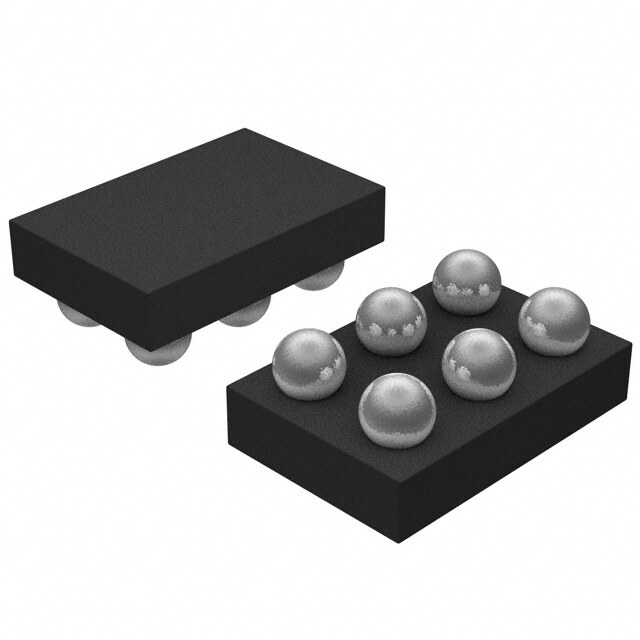
| 产品图片 |
|
| rohs | 符合RoHS无铅 / 符合限制有害物质指令(RoHS)规范要求 |
| 产品系列 | 电源管理 IC,稳压器—开关式稳压器,Texas Instruments TPS61256YFFR- |
| 数据手册 | |
| 产品型号 | TPS61256YFFR |
| PWM类型 | 电流模式 |
| 产品种类 | 稳压器—开关式稳压器 |
| 供应商器件封装 | 9-DSBGA(1.2x1.3) |
| 关闭 | Shutdown |
| 其它名称 | 296-29824-1 |
| 包装 | 剪切带 (CT) |
| 同步整流器 | 是 |
| 商标 | Texas Instruments |
| 安装类型 | 表面贴装 |
| 安装风格 | SMD/SMT |
| 封装 | Reel |
| 封装/外壳 | 9-UFBGA,DSBGA |
| 封装/箱体 | DSBGA-9 |
| 工作温度 | -40°C ~ 85°C |
| 工作温度范围 | - 40 C to + 85 C |
| 工厂包装数量 | 3000 |
| 开关频率 | 3.5 MHz |
| 拓扑结构 | Boost |
| 最大工作温度 | + 85 C |
| 最大输入电压 | 4.85 V |
| 最小工作温度 | - 40 C |
| 最小输入电压 | 2.5 V |
| 标准包装 | 1 |
| 电压-输入 | 2.5 V ~ 4.35 V |
| 电压-输出 | 5V |
| 电流-输出 | 900mA |
| 电源电压-最小 | 2.5 V |
| 电源电流 | 30 uA |
| 类型 | 升压(升压) |
| 系列 | TPS61256 |
| 输入电压 | 2.5 V to 4.85 V |
| 输出数 | 1 |
| 输出电压 | 5 V |
| 输出电流 | 900 mA |
| 输出端数量 | 1 Output |
| 输出类型 | 固定 |
| 配用 | /product-detail/zh/TPS61256EVM-711/296-31244-ND/2797914 |
| 频率-开关 | 3.5MHz |


- 商务部:美国ITC正式对集成电路等产品启动337调查
- 曝三星4nm工艺存在良率问题 高通将骁龙8 Gen1或转产台积电
- 太阳诱电将投资9.5亿元在常州建新厂生产MLCC 预计2023年完工
- 英特尔发布欧洲新工厂建设计划 深化IDM 2.0 战略
- 台积电先进制程称霸业界 有大客户加持明年业绩稳了
- 达到5530亿美元!SIA预计今年全球半导体销售额将创下新高
- 英特尔拟将自动驾驶子公司Mobileye上市 估值或超500亿美元
- 三星加码芯片和SET,合并消费电子和移动部门,撤换高东真等 CEO
- 三星电子宣布重大人事变动 还合并消费电子和移动部门
- 海关总署:前11个月进口集成电路产品价值2.52万亿元 增长14.8%


PDF Datasheet 数据手册内容提取
Product Sample & Technical Tools & Support & Folder Buy Documents Software Community TPS61253,TPS61254,TPS61256,TPS61258,TPS61259,TPS612592 SLVSAG8G–SEPTEMBER2011–REVISEDJUNE2016 TPS6125x 3.5-MHz High Efficiency Step-Up Converter In Chip Scale Packaging 1 Features The TPS6125x operates at a regulated 3.5-MHz switching frequency and enters power-save mode • 93%Efficiencyat3.5-MHzOperation 1 operation at light load currents to maintain high • 21-µAQuiescentCurrentinStandbyMode efficiency over the entire load current range. The • 37-µAQuiescentCurrentinNormalOperation PFM mode extends the battery life by reducing the quiescent current to 37 μA (typ) during light load • WideV RangeFrom2.3Vto5.5V IN operation. • V ≥V Operation IN OUT In addition, the TPS6125x device can also maintain • I ≥800mAatV =4.5V,V ≥2.65V OUT OUT IN its output biased at the input voltage level. In this • IOUT≥1000mAatVOUT=5.0V,VIN ≥ 3.3V mode, the synchronous rectifier is current limited • I ≥1500mA(Peak)atV =5.0V,V ≥ 3.3 allowing external load (e.g. audio amplifier) to be OUT OUT IN V powered with a restricted supply. In this mode, the quiescent current is reduced to 21 µA. During • ±2%TotalDCVoltageAccuracy shutdown, the load is completely disconnected from • Light-LoadPFMMode the battery. Input current in shutdown mode is less • SelectableStandbyModeorTrueLoad than1µA(typ),whichmaximizesbatterylife. DisconnectDuringShutdown The TPS6125x offers a very small solution size due • ThermalShutdownandOverloadProtection to minimum amount of external components. It allows • OnlyThreeSurface-MountExternalComponents the use of small inductors and input capacitors to Required achieveasmallsolutionsize. • TotalSolutionSize <25mm2 DeviceInformation(1) • 9-PinNanoFreeTM(CSP)Packaging PARTNUMBER PACKAGE BODYSIZE(NOM) TPS6125x DSBGA(9) 1.206mm×1.306mm 2 Applications (1) For all available packages, see the orderable addendum at • CellPhones,SmartPhones theendofthedatasheet. • MonoandStereoAPAApplications EfficiencyvsLoadCurrent • USBChargingPorts(5V) 3 Description 100 VO= 5.0 V The TPS6125x device provides a power supply 90 solution for battery-powered portable applications. 80 Intended for low-power applications, the TPS6125x supports up to 800-mA load current from a battery 70 dcWoisistchthcaahriwgpeididnedaiusncpltoouwrt vaaonsldta2cg.6ae5prVaacnaitgnoedrsoa.fllo2w.3sVthteou5s.5eVof,ltohwe Efficiency - %654000 . device supports applications powered by Li-Ion 30 batteries with extended voltage range. Different fixed 20 voltage output versions are available from 3.15 V to 10 5.0V. 0 5.4 5.1V4.8I- In4.5put 4.2Volta3.9ge - 3.6V 3.3 3.0 27..0.10.2 0.4 0.8 1.6I3.2O- O6.2utp12.6ut C25.1urr50.1ent -100.1 mA199.6398.1794.3 1 An IMPORTANT NOTICE at the end of this data sheet addresses availability, warranty, changes, use in safety-critical applications, intellectualpropertymattersandotherimportantdisclaimers.UNLESSOTHERWISENOTED,thisdocumentcontainsPRODUCTION DATA.
TPS61253,TPS61254,TPS61256,TPS61258,TPS61259,TPS612592 SLVSAG8G–SEPTEMBER2011–REVISEDJUNE2016 www.ti.com Table of Contents 1 Features.................................................................. 1 10 ApplicationandImplementation........................ 19 2 Applications........................................................... 1 10.1 ApplicationInformation..........................................19 3 Description............................................................. 1 10.2 TypicalApplication................................................19 4 RevisionHistory..................................................... 2 10.3 SystemExamples.................................................24 5 DeviceOptions....................................................... 4 11 PowerSupplyRecommendations..................... 26 6 PinConfigurationandFunctions......................... 4 12 Layout................................................................... 26 12.1 LayoutGuidelines.................................................26 7 Specifications......................................................... 5 12.2 LayoutExample....................................................26 7.1 AbsoluteMaximumRatings......................................5 12.3 ThermalConsiderations........................................27 7.2 ESDRatings..............................................................5 13 DeviceandDocumentationSupport................. 28 7.3 RecommendedOperatingConditions.......................5 7.4 ThermalInformation..................................................6 13.1 DeviceSupport......................................................28 7.5 ElectricalCharacteristics...........................................6 13.2 RelatedLinks........................................................28 7.6 TypicalCharacteristics..............................................9 13.3 ReceivingNotificationofDocumentationUpdates28 13.4 CommunityResources..........................................28 8 ParameterMeasurementInformation................14 13.5 Trademarks...........................................................28 9 DetailedDescription............................................ 15 13.6 ElectrostaticDischargeCaution............................28 9.1 Overview.................................................................15 13.7 Glossary................................................................28 9.2 FunctionalBlockDiagram.......................................15 14 Mechanical,Packaging,andOrderable 9.3 FeatureDescription.................................................16 Information........................................................... 29 9.4 DeviceFunctionalModes........................................17 14.1 PackageSummary................................................29 4 Revision History NOTE:Pagenumbersforpreviousrevisionsmaydifferfrompagenumbersinthecurrentversion. ChangesfromRevisionF(March2016)toRevisionG Page • ChangedthePackageDimensionssection.......................................................................................................................... 29 ChangesfromRevisionE(March2015)toRevisionF Page • AddeddeviceTPS612592...................................................................................................................................................... 4 ChangesfromRevisionD(December2014)toRevisionE Page • ChangedBodySize(NOM)from"1.60mm×1.60"to"1.206mm×1.306"intheDeviceInformationtable......................1 • AddedtablenotereferencetoThird-PartyProductsDisclaimer.......................................................................................... 19 ChangesfromRevisionC(August2012)toRevisionD Page • AddedESDRatingstable,FeatureDescriptionsection,DeviceFunctionalModes,ApplicationandImplementation section,PowerSupplyRecommendationssection,Layoutsection,DeviceandDocumentationSupportsection,and Mechanical,Packaging,andOrderableInformationsection.................................................................................................. 1 ChangesfromRevisionB(May2012)toRevisionC Page • AddedTPS61259todatasheetheaderasproductiondevice............................................................................................... 1 • ChangeddeviceTPS61259toproductionstatus................................................................................................................... 4 2 SubmitDocumentationFeedback Copyright©2011–2016,TexasInstrumentsIncorporated ProductFolderLinks:TPS61253 TPS61254 TPS61256 TPS61258 TPS61259 TPS612592
TPS61253,TPS61254,TPS61256,TPS61258,TPS61259,TPS612592 www.ti.com SLVSAG8G–SEPTEMBER2011–REVISEDJUNE2016 ChangesfromRevisionA(October2011)toRevisionB Page • AddedTPS61253andTPS61258todatasheetheaderasproductiondevices.................................................................... 1 • ChangeddevicesTPS61253andTPS61258toproductionstatus........................................................................................ 4 • ChangedgraphicentityforFigure3..................................................................................................................................... 10 • ChangedgraphicentityforFigure10andFigure13............................................................................................................ 11 • ChangedgraphicentityforFigure23................................................................................................................................... 13 Copyright©2011–2016,TexasInstrumentsIncorporated SubmitDocumentationFeedback 3 ProductFolderLinks:TPS61253 TPS61254 TPS61256 TPS61258 TPS61259 TPS612592
TPS61253,TPS61254,TPS61256,TPS61258,TPS61259,TPS612592 SLVSAG8G–SEPTEMBER2011–REVISEDJUNE2016 www.ti.com 5 Device Options T PARTNUMBER(1) OUTPUT DEVICE A VOLTAGE SPECIFICFEATURES Supports5V,upto1500mApeakloading TPS61253 5.0V downto3.3Vinputvoltage Supports4.5V/800mAloading TPS61254 4.5V downto2.65Vinputvoltage TPS61255(2) 3.75V Supports5V/900mAloading TPS61256 5.0V downto3.3Vinputvoltage –40°Cto85°C TPS61257(2) 4.3V Supports4.5V,upto1500mApeakloading TPS61258 4.5V downto3.3Vinputvoltage Supports5.1V,upto1500mApeakloading TPS61259 5.1V downto3.3Vinputvoltage Supports5.2V,upto1500mApeakloading TPS612592 5.2V downto3.3Vinputvoltage (1) Forallavailablepackages,seetheorderableaddendumattheendofthedatasheet. (2) Productpreview.ContactTIfactoryformoreinformation 6 Pin Configuration and Functions A1 A2 A3 A3 A2 A1 B1 B2 B3 B3 B2 B1 C1 C2 C3 C3 C2 C1 PinFunctions PIN I/O DESCRIPTION NAME NO. Thisisthemodeselectionpinofthedeviceandisonlyofrelevancewhenthedeviceisdisabled (EN=Low).Thispinmustnotbeleftfloatingandmustbeterminated.RefertoTable2formore details. BP C3 I BP=Low:Thedeviceisintrueshutdownmode. BP=High:Theoutputisbiasedattheinputvoltagelevelwithamaximumloadcurrentcapabilityof ca.150mA.Instandbymode,thedeviceonlyconsumesastandbycurrentof21µA(typ). Thisistheenablepinofthedevice.Connectingthispintogroundforcesthedeviceintoshutdown EN B3 I mode.Pullingthispinhighenablesthedevice.Thispinmustnotbeleftfloatingandmustbe terminated. GND C1,C2 Groundpin. SW B1,B2 I/O ThisistheswitchpinoftheconverterandisconnectedtothedrainoftheinternalPowerMOSFETs. VIN A3 I Powersupplyinput. VOUT A1,A2 O Boostconverteroutput. 4 SubmitDocumentationFeedback Copyright©2011–2016,TexasInstrumentsIncorporated ProductFolderLinks:TPS61253 TPS61254 TPS61256 TPS61258 TPS61259 TPS612592
TPS61253,TPS61254,TPS61256,TPS61258,TPS61259,TPS612592 www.ti.com SLVSAG8G–SEPTEMBER2011–REVISEDJUNE2016 7 Specifications 7.1 Absolute Maximum Ratings overoperatingfree-airtemperaturerange(unlessotherwisenoted)(1) MIN MAX UNIT Inputvoltage VoltageatVIN(2),VOUT(2),SW(2),EN(2),BP(2) –0.3 7 V ContinuousaveragecurrentintoSW (3) 1.8 Inputcurrent A PeakcurrentintoSW (4) 3.5 Powerdissipation Internallylimited Operating,T (5) –40 85 A Temperature Operatingvirtualjunction,T –40 150 °C J Storage,T –65 150 stg (1) Stressesbeyondthoselistedunderabsolutemaximumratingsmaycausepermanentdamagetothedevice.Thesearestressratings only,andfunctionaloperationofthedeviceattheseoranyotherconditionsbeyondthoseindicatedunderrecommendedoperating conditionsisnotimplied.Exposuretoabsolute-maximum-ratedconditionsforextendedperiodsmyaffectdevicereliability. (2) Allvoltagesarewithrespecttonetworkgroundterminal. (3) Limitthejunctiontemperatureto105°Cforcontinuousoperationatmaximumoutputpower. (4) Limitthejunctiontemperatureto125°Cfor5%dutycycleoperation. (5) Inapplicationswherehighpowerdissipationand/orpoorpackagethermalresistanceispresent,themaximumambienttemperaturemay havetobederated.Maximumambienttemperature(T )isdependentonthemaximumoperatingjunctiontemperature(T ),the A(max) J(max) maximumpowerdissipationofthedeviceintheapplication(P ),andthejunction-to-ambientthermalresistanceofthepart/package D(max) intheapplication(θ ),asgivenbythefollowingequation:T =T –(θ XP ).Toachieveoptimumperformance,itis JA A(max) J(max) JA D(max) recommendedtooperatethedevicewithamaximumjunctiontemperatureof105°C. 7.2 ESD Ratings VALUE UNIT Human-bodymodel(HBM),perANSI/ESDA/JEDECJS-001(1) ±2000 Charged-devicemodel(CDM),perJEDECspecificationJESD22- ±1000 V(ESD) Electrostaticdischarge C101(2) V Machinemodel(MM) ±200 (1) JEDECdocumentJEP155statesthat500-VHBMallowssafemanufacturingwithastandardESDcontrolprocess.Manufacturingwith lessthan500-VHBMispossiblewiththenecessaryprecautions. (2) JEDECdocumentJEP157statesthat250-VCDMallowssafemanufacturingwithastandardESDcontrolprocess.Manufacturingwith lessthan250-VCDMispossiblewiththenecessaryprecautions. 7.3 Recommended Operating Conditions MIN NOM MAX UNIT TPS61253 2.65(1) 4.85 TPS61254 2.5 4.35 TPS61256 2.5 4.85 V Inputvoltagerange TPS61257 2.5 4.15 V I TPS61258 2.65(1) 4.35 TPS61259 2.65(1) 4.85 TPS612592 2.65(1) 4.85 R Minimumresistiveloadforstart-up TPS6125x 55 Ω L L Inductance 0.7 1.0 2.9 µH C Outputcapacitance 3.5 5 50 µF O T Ambienttemperature –40 85 °C A T Operatingjunctiontemperature –40 125 °C J (1) Upto1000mApeakoutputcurrent. Copyright©2011–2016,TexasInstrumentsIncorporated SubmitDocumentationFeedback 5 ProductFolderLinks:TPS61253 TPS61254 TPS61256 TPS61258 TPS61259 TPS612592
TPS61253,TPS61254,TPS61256,TPS61258,TPS61259,TPS612592 SLVSAG8G–SEPTEMBER2011–REVISEDJUNE2016 www.ti.com 7.4 Thermal Information TPS6125x THERMALMETRIC(1) YFF UNIT 9PINS R Junction-to-ambientthermalresistance 108.3 θJA R Junction-to-case(top)thermalresistance 1.0 θJC(top) R Junction-to-boardthermalresistance 18 °C/W θJB ψ Junction-to-topcharacterizationparameter 4.2 JT ψ Junction-to-boardcharacterizationparameter 17.9 JB (1) Formoreinformationabouttraditionalandnewthermalmetrics,seetheSemiconductorandICPackageThermalMetricsapplication report. 7.5 Electrical Characteristics MinimumandmaximumvaluesareatV =2.3Vto5.5V,EN=1.8V,T =–40°Cto85°C;CircuitofParameterMeasurement IN A Informationsection(unlessotherwisenoted).TypicalvaluesareatV =3.6V,EN=1.8V,T =25°C(unlessotherwise IN A noted). PARAMETER TESTCONDITIONS MIN TYP MAX UNIT SUPPLYCURRENT I =0mA,V =3.6V 30 45 µA OUT IN Operatingquiescentcurrent EN=V ,BP=GND IN intoVINOperatingquiescentcurrent Devicenotswitching 7 15 µA IQ intoVOUTStandbymodequiescentcurrent I =0mA,V =V =3.6V 11 20 µA intoV Standbymodequiescentcurrent OUT IN OUT IN intoVOUT EN=GND,BP=VIN 9.5 15 µA Devicenotswitching I Shutdowncurrent EN=GND,BP=GND 0.85 5.0 μA SD Falling 2.0 2.1 V V Under-voltagelockoutthreshold UVLO Hysteresis 0.1 V ENABLE,BYPASS V Low-levelinputvoltage 0.4 V IL V High-levelinputvoltage 1.0 V IH I Inputleakagecurrent InputconnectedtoGNDorV 0.5 µA lkg IN 6 SubmitDocumentationFeedback Copyright©2011–2016,TexasInstrumentsIncorporated ProductFolderLinks:TPS61253 TPS61254 TPS61256 TPS61258 TPS61259 TPS612592
TPS61253,TPS61254,TPS61256,TPS61258,TPS61259,TPS612592 www.ti.com SLVSAG8G–SEPTEMBER2011–REVISEDJUNE2016 Electrical Characteristics (continued) MinimumandmaximumvaluesareatV =2.3Vto5.5V,EN=1.8V,T =–40°Cto85°C;CircuitofParameterMeasurement IN A Informationsection(unlessotherwisenoted).TypicalvaluesareatV =3.6V,EN=1.8V,T =25°C(unlessotherwise IN A noted). PARAMETER TESTCONDITIONS MIN TYP MAX UNIT OUTPUT 2.3V≤V ≤4.85V,I =0mA IN OUT 4.92 5 5.08 PWMoperation.OpenLoop 3.3V≤V ≤4.85V,0mA≤I ≤1000mA IN OUT 4.85 5 5.2 PFM/PWMoperation RegulatedDCoutputvoltage TPS61253 V 3.3V≤V ≤4.85V,0mA≤I ≤1500mA IN OUT PFM/PWMoperation 4.75 5 5.2 Pulsedloadtest;Pulsewidth≤20ms; Dutycycle≤10% 2.3V≤V ≤4.35V,I =0mA IN OUT 4.43 4.5 4.57 PWMoperation.OpenLoop RegulatedDCoutputvoltage TPS61254 V 2.65V≤V ≤4.35V,0mA≤I ≤800mA IN OUT 4.4 4.5 4.65 PFM/PWMoperation 2.3V≤V ≤4.85V,I =0mA IN OUT 4.92 5 5.08 PWMoperation.OpenLoop RegulatedDCoutputvoltage TPS61256 V 2.65V≤V ≤4.85V,0mA≤I ≤700mA IN OUT 4.9 5 5.2 PFM/PWMoperation VOUT 2.3V≤VIN≤4.15V,IOUT=0mA 4.23 4.3 4.37 PWMoperation.Openloop. RegulatedDCoutputvoltage TPS61257 V 2.65V≤V ≤4.15V,0mA≤I ≤800mA IN OUT 4.2 4.3 4.45 PFM/PWMoperation 2.3V≤V ≤4.35V,I =0mA IN OUT 4.43 4.5 4.57 PWMoperation.OpenLoop RegulatedDCoutputvoltage TPS61258 3.3V≤VIN≤4.35V,0mA≤IOUT≤1500mA V PFM/PWMoperation 4.3 4.5 4.65 Pulsedloadtest;Pulsewidth≤20ms; Dutycycle≤10% 2.3V≤V ≤4.85V,I =0mA IN OUT 5.02 5.1 5.18 PWMoperation.OpenLoop RegulatedDCoutputvoltage TPS61259 3.4V≤VIN≤4.85V,0mA≤IOUT≤1500mA V PFM/PWMoperation 4.75 5.1 5.3 Pulsedloadtest;Pulsewidth≤20ms; Dutycycle≤10% 2.7V≤V ≤4.8V,I =0mA RegulatedDCoutputvoltage TPS612592 IN OUT 5.1 5.2 5.3 V PWMoperation.OpenLoop Power-savemodeoutputripple PFMoperation,I =1mA 45 voltage OUT TPS61254 Standbymodeoutputripple mVpk voltage TPS61258 EN=GND,BP=VIN,IOUT=0mA 80 ΔV PWMmodeoutputripplevoltage PWMoperation,I =200mA 20 OUT OUT Power-savemodeoutputripple TPS61253 PFMoperation,I =1mA 50 voltage TPS61256 OUT mVpk Standbymodeoutputripple TPS61259 EN=GND,BP=V ,I =0mA 80 voltage TPS612592 IN OUT Copyright©2011–2016,TexasInstrumentsIncorporated SubmitDocumentationFeedback 7 ProductFolderLinks:TPS61253 TPS61254 TPS61256 TPS61258 TPS61259 TPS612592
TPS61253,TPS61254,TPS61256,TPS61258,TPS61259,TPS612592 SLVSAG8G–SEPTEMBER2011–REVISEDJUNE2016 www.ti.com Electrical Characteristics (continued) MinimumandmaximumvaluesareatV =2.3Vto5.5V,EN=1.8V,T =–40°Cto85°C;CircuitofParameterMeasurement IN A Informationsection(unlessotherwisenoted).TypicalvaluesareatV =3.6V,EN=1.8V,T =25°C(unlessotherwise IN A noted). PARAMETER TESTCONDITIONS MIN TYP MAX UNIT POWERSWITCH High-sideMOSFETonresistance 170 r mΩ DS(on) Low-sideMOSFETonresistance 100 I ReverseleakagecurrentintoVOUT EN=GND,BP=GND 3.5 µA lkg TPS61253 TPS61258 EN=V ,BP=GND.OpenLoop 3300 3620 3900 TPS61259 IN Switchvalleycurrentlimit TPS612592 mA I TPS61254 LIM TPS61256 EN=V ,BP=GND.OpenLoop 1900 2150 2400 IN TPS61257 Pre-chargemodecurrentlimit EN=GND,BP=V 165 215 265 mA (linearmode) IN Overtemperatureprotection 140 °C Overtemperaturehysteresis 20 °C OSCILLATOR f Oscillatorfrequency V =3.6VV =4.5V 3.5 MHz OSC IN OUT TIMING BP=GND,I =0mA. TPS6125x OUT 70 µs TimefromactiveENtostartswitching TPS61253 Start-uptime TPS61254 TPS61256 BP=GND,I =0mA. OUT 400 µs TPS61258 TimefromactiveENtoV OUT TPS61259 TPS612592 8 SubmitDocumentationFeedback Copyright©2011–2016,TexasInstrumentsIncorporated ProductFolderLinks:TPS61253 TPS61254 TPS61256 TPS61258 TPS61259 TPS612592
TPS61253,TPS61254,TPS61256,TPS61258,TPS61259,TPS612592 www.ti.com SLVSAG8G–SEPTEMBER2011–REVISEDJUNE2016 7.6 Typical Characteristics Table1.TableofGraphs FIGURE vsOutputcurrent Figure1,Figure2, η Efficiency Figure3,Figure5 vsInputvoltage Figure4 vsOutputcurrent Figure6,Figure7, Figure8,Figure9, V DCoutputvoltage Figure10, O Figure14 vsInputvoltage Figure11 vsInputvoltage Figure12, I Maximumoutputcurrent O Figure13 vsOutputcurrent Figure15, ΔV Peak-to-peakoutputripplevoltage Figure16, O Figure17 vsInputvoltage Figure18, I Supplycurrent CC Figure19 vsDifferentialinput-outputvoltage Figure20, DCpre-chargecurrent Figure21 I LIM vsTemperature Figure22, Valleycurrentlimit Figure23 r MOSFETr vsTemperature Figure24 DS(on) DS(on) 100 100 V = 4.5 V VO= 5 V (TPS61256) VI= 4.5 V 95 I 95 PFM/PWM Operation 90 90 85 V = 3.3 V 85 % I V = 3.6 V Efficiency - 778050 VI= 2.5 V VI= 2.7 V VI= 3 V VI= 3.6 V Efficiency - % 778050 VI= 2V.5I V= 2.7 VVI= 3 V VI= 3.3 VI 65 65 60 60 55 VO= 4.5 V 55 PFM/PWM Operation 50 50 0.1 1 10 100 1000 0.1 1 10 100 1000 IO- Output Current - mA IO- Output Current - mA Figure1.EfficiencyvsOutputCurrent Figure2.EfficiencyvsOutputCurrent Copyright©2011–2016,TexasInstrumentsIncorporated SubmitDocumentationFeedback 9 ProductFolderLinks:TPS61253 TPS61254 TPS61256 TPS61258 TPS61259 TPS612592
TPS61253,TPS61254,TPS61256,TPS61258,TPS61259,TPS612592 SLVSAG8G–SEPTEMBER2011–REVISEDJUNE2016 www.ti.com 100 100 95 VI= 4.2 V VI= 4.5 V 98 VPFOM=/ P5 WVM Operation 96 90 94 IO= 300 mA 92 85 V = 3.6 V VI= 3.3 V I 90 Efficiency - % 778050 Efficiency - % 88882468 I = 800 mAIO= 100 mA IO= 10 mA 80 O 65 78 60 76 V = 5 V (TPS61253), 55 IOO= Pulse Operation (tpulse= 20 ms,d= 10%), 74 PFM/PWM Operation 72 50 70 0 1 10 100 1000 10000 2.52.72.93.13.33.53.73.94.14.34.54.74.95.15.35.5 IO- Output Current - mA VI- Input Voltage - V Figure3.EfficiencyvsOutputCurrent Figure4.EfficiencyvsInputVoltage 100 4.59 V = 2.7 V I V = 4.5 V I 90 V = 3.3 V I 80 VI= 3 V 4.55 V y - % 6700 VI= 4.5 V VI= 3.6 V Voltage - VI= 2.5 V nc 50 ut 4.50 e p Effici 40 C Out VI= 3.6 V D 30 - O V 4.46 20 10 VO~ VI VO= 4.5 V Standby Operation PFM/PWM Operation 0 4.41 0.01 0.1 1 10 100 0.1 1 10 100 1000 IO- Output Current - mA IO- Output Current - mA Figure5.EfficiencyvsOutputCurrent Figure6.DCOutputVoltagevsOutputCurrent 5.15 4.545 VO= 5 V (TPS61256) VO= 4.5 V PFM/PWM Operation PWM Operation V = 4.5 V Output Voltage - V 5.50.51 VI= 4.5 VVI= 5 V Output Voltage - V 4.445.55 VVIVI==I =22 ..357 VVV I - DC O VI= 3.6 V VI= 2.5 V - DC O VVI== 33..63 VV V 5 V 4.41 I V = 4.2 V I 4.95 4.365 0.1 1 10 100 1000 500 700 900 1100 1300 1500 1700 1900 IO- Output Current - mA IO- Output Current - mA Figure7.DCOutputVoltagevsOutputCurrent Figure8.DCOutputVoltagevsOutputCurrent 10 SubmitDocumentationFeedback Copyright©2011–2016,TexasInstrumentsIncorporated ProductFolderLinks:TPS61253 TPS61254 TPS61256 TPS61258 TPS61259 TPS612592
TPS61253,TPS61254,TPS61256,TPS61258,TPS61259,TPS612592 www.ti.com SLVSAG8G–SEPTEMBER2011–REVISEDJUNE2016 5.05 5.1 VO= 5 V (TPS61256) VO= 5 V (TPS61253), PWM Operation V = 3.6 V IO= Pulse Operation (tpulse= 20 ms,d= 10%), I VI= 4.2 V 5.05 PWM Operation 5 VI= 4.5 V VI= 4.2 V VI= 4.5 V V V 5 e - VI= 2.5 V e - g g ut Volta 4.95 VVII== 32 .V7 V ut Volta 4.95 VI= 3 V Outp 4.9 VI= 3.3 V Outp 4.9 VI= 3.3 V V- DC O V- DC O4.85 VI= 3.6 V 4.85 4.8 4.8 500 700 900 1100 1300 1500 1700 1900 4.75 10001100120013001400150016001700180019002000 I - Output Current - mA O I - Output Current - mA O Figure9.DCOutputVoltagevsOutputCurrent Figure10.DCOutputVoltagevsOutputCurrent 5.55 2300 V = 5 V O V = 5 V (TPS61256) 5.5 PFM/PWM Operation 2100 PWOM Operation 5.45 A utput Voltage - V 55..5523..5534 IO=I O50=0 8 m00A mA Output Current - m 1111357900000000 TA= 25°CTA= -40T°CA= 85°C O 5.2 m C u D m 1100 V- O5.51.51 IO= 10 mA IO= 100 mA - Maxi 900 O 5.05 I 700 5 500 4.95 2.52.72.93.13.33.53.73.94.14.34.54.74.95.15.35.5 2.5 2.75 3 3.25 3.5 3.75 4 4.25 4.5 4.75 5 VI- Input Voltage - V VI- Input Voltage - V Figure11.DCOutputVoltagevsInputVoltage Figure12.MaximumOutputCurrentvsInputVoltage 3000 5 V ~ V 4.8 O I 2800 V = 4.5 V Standby Operation 4.6 I A 2600 m 4.4 VI= 4.2 V I- Maximum Output Current - O 1111222246802400000000000000 TA= 25T A°C= -40 °CTA= 85 °C TA= 65 °C V- DC Output Voltage - VO2233334.......683246842 VVVVIIII==== 3323... 367V VVV 1000 VIO== P 5u Vls e(T OPpSe6r1a2t5io3n), (t = 20 ms,d= 10%) 2.4 VI= 2.5 V O pulse 2.2 PWM Operation 800 2 2.5 2.75 3 3.25 3.5 3.75 4 4.25 4.5 4.75 5 0 20 40 60 80 100120140160180200220240 VI- Input Voltage - V IO- Output Current - mA Figure13.MaximumOutputCurrentvsInputVoltage Figure14.DCOutputVoltagevsOutputCurrent Copyright©2011–2016,TexasInstrumentsIncorporated SubmitDocumentationFeedback 11 ProductFolderLinks:TPS61253 TPS61254 TPS61256 TPS61258 TPS61259 TPS612592
TPS61253,TPS61254,TPS61256,TPS61258,TPS61259,TPS612592 SLVSAG8G–SEPTEMBER2011–REVISEDJUNE2016 www.ti.com 60 60 V = 5 V (TPS61256) O V = 5 V (TPS61256) mV 55 PFM/PWM Operation VI= 2.7 V mV 55 PFOM/PWM Operation e - 50 e - 50 g V = 3.3 V g olta 45 I olta 45 VI= 2.7 V ple V 40 VI= 3.6 V ple V 40 VI= 3.3 V p p Ri 35 Ri 35 V = 3.6 V utput 30 utput 30 VI= 4.I5 V k O 25 VI= 4.5 V k O 25 a a Pe 20 Pe 20 o- o- k-t 15 k-t 15 a a Pe 10 Pe 10 - - VO 5CO= 10μF 6.3V (0603) X5R, muRataGRM188R60J106ME84D VO 5 CO= 22μF 10V (1210) X5R, muRata GRM32ER71A226K 0 0 0 100 200 300 400 500 600 700 800 900 1000 0 100 200 300 400 500 600 700 800 900 1000 IO- Output Current - mA IO- Output Current - mA Figure15.Peak-to-PeakOutputRippleVoltagevsOutput Figure16.Peak-to-PeakOutputRippleVoltagevsOutput Current Current 60 80 V = 5 V (TPS61253) mV 55 PFOM/PWM Operation 75 VO= 5 V e - 50 70 IO= 0 mA g a olt 45 65 ple V 40 VI= 3.3 V A 60 TA= 85°C Output Rip 233505 VI= 3.6 V Current -m 455505 TA= 25°C Peak 20 pply 40 ak-to- 15 VI= 4.5 V Su 3305 TA= -40°C Pe 10 - CO = x2 10mF 6.3 V (0603) X5R, 25 VO 5 muRata GRM188R60J106ME84D 20 0 0 200 400 600 800 1000 1200 1400 15 I - Output Current - mA 2.5 2.7 2.9 3.1 3.3 3.5 3.7 3.9 4.1 4.3 4.5 4.7 4.9 O V - Input Voltage - V I Figure17.Peak-to-PeakOutputRippleVoltagevsOutput Figure18.SupplyCurrentvsInputVoltage Current 45 250 VI~ VO 245 40 IO= 0 mA T = -40°C 240 Standby Operation A 235 230 ent -Am 233505 TA= 85°C TA= 25°C urrent - mA 222220112250505 TVAI== 4 2.55 °VC, TVAI== 2 2.75 °VC, pply Curr 20 Charge C 112990050 VI= 3.6 V, Su 15 Pre- 118805 TA= 25°C C 175 10 D 170 165 5 160 155 0 150 2.52.72.93.13.33.53.73.94.14.34.54.74.95.15.35.5 0 0.30.60.91.21.51.82.12.4 2.7 3 3.33.63.94.24.5 VI- Input Voltage - V Differential Input - Output Voltage - V Figure19.SupplyCurrentvsInputVoltage Figure20.DCPre-ChargeCurrentvsDifferentialInput- OutputVoltage 12 SubmitDocumentationFeedback Copyright©2011–2016,TexasInstrumentsIncorporated ProductFolderLinks:TPS61253 TPS61254 TPS61256 TPS61258 TPS61259 TPS612592
TPS61253,TPS61254,TPS61256,TPS61258,TPS61259,TPS612592 www.ti.com SLVSAG8G–SEPTEMBER2011–REVISEDJUNE2016 250 25 245 V = 3.6 V Sample Size = 200 IN 240 235 T = 130°C 230 20 J urrent - mA 222220112250505 TVAI== 3 8.65 °VC, TVAI== 3 2.65 °VC, ntage - %15 TTJJ== - 2205°°CC C e harge 112990050 e Perc10 C V = 3.6 V, pl e- 185 I m Pr 180 TA= -40°C Sa C 175 D 170 5 165 160 155 150 0 0 0.3 0.6 0.9 1.2 1.5 1.8 2.1 2.4 2.7 3 3.3 3.6 002550750025507500255075002550750025507500 Differential Input - Output Voltage - V 191919192020202021212121222222222323232324 I - Valley Current Limit - mA Figure21.DCPre-ChargeCurrentvsDifferentialInput- LIM OutputVoltage Figure22.ValleyCurrentLimit 25 200 TPS61253 V = 5 V V = 3.6 V, O IN 180 Sample Size = 200 T = 125°C J 20 160 Rectifier MOSFET W T = 25°C m centage - %15 J sistance - 112400 mple Per10 TJ= -20°C - On-Re 10800 Switch MOSFET a n) S S(o 60 D 5 R 40 20 0 00255075002550750025507500255075002550750025507500 0 33333333343434343535353536363636373737373838383839 -30 -10 10 30 50 70 90 110 130 ILIM- Valley Current Limit - mA TJ- Junction Temperature - °C Figure23.ValleyCurrentLimit Figure24.MOSFETr vsTemperature DS(on) Copyright©2011–2016,TexasInstrumentsIncorporated SubmitDocumentationFeedback 13 ProductFolderLinks:TPS61253 TPS61254 TPS61256 TPS61258 TPS61259 TPS612592
TPS61253,TPS61254,TPS61256,TPS61258,TPS61259,TPS612592 SLVSAG8G–SEPTEMBER2011–REVISEDJUNE2016 www.ti.com 8 Parameter Measurement Information TPS6125x L SW VOUT V 1μH OUT V VIN BP IN C O C 10 uF I EN GND 4.7μF EN BP Shutdown, True Load Disconnect (SD) 0 0 Standby Mode, Output Pre-Biased (SM) 0 1 Boost Operating Mode (BST) 1 X Figure25. ParameterMeasurementSchematic 14 SubmitDocumentationFeedback Copyright©2011–2016,TexasInstrumentsIncorporated ProductFolderLinks:TPS61253 TPS61254 TPS61256 TPS61258 TPS61259 TPS612592
TPS61253,TPS61254,TPS61256,TPS61258,TPS61259,TPS612592 www.ti.com SLVSAG8G–SEPTEMBER2011–REVISEDJUNE2016 9 Detailed Description 9.1 Overview The TPS6125x synchronous step-up converter typically operates at a quasi-constant 3.5-MHz frequency pulse width modulation (PWM) at moderate to heavy load currents. At light load currents, the TPS6125x converter operatesinpower-savemodewithpulsefrequencymodulation(PFM). DuringPWMoperation,theconverterusesanovelquasi-constanton-timevalleycurrentmodecontrolschemeto achieve excellent line/load regulation and allows the use of a small ceramic inductor and capacitors. Based on theV /V ratio,asimplecircuitpredictstherequiredon-time. IN OUT At the beginning of the switching cycle, the low-side N-MOS switch is turned-on and the inductor current ramps up to a peak current that is defined by the on-time and the inductance. In the second phase, once the on-timer has expired, the rectifier is turned-on and the inductor current decays to a preset valley current threshold. Finally, theswitchingcyclerepeatsbysettingtheontimeragainandactivatingthelow-sideN-MOSswitch. In general, a dc/dc step-up converter can only operate in "true" boost mode, i.e. the output “boosted” by a certain amount above the input voltage. The TPS6125x device operates differently as it can smoothly transition in and out of zero duty cycle operation. Therefore the output can be kept as close as possible to its regulation limits even though the converter is subject to an input voltage that tends to be excessive. In this operation mode, the outputcurrentcapabilityoftheregulatorislimitedtoca.150mA.RefertoFigure11 forfurtherdetails. The current mode architecture with adaptive slope compensation provides excellent transient load response, requiring minimal output filtering. Internal soft-start and loop compensation simplifies the design process while minimizingthenumberofexternalcomponents. 9.2 Functional Block Diagram SW VOUT VIN er NMOS PMOS v Dri Valley e Current at Sense G Modulator Errormplifier A Softstart V REF Thermal EN Shutdown Control Logic Undervoltage BP Lockout GND Copyright © 2016,Texas Instruments Incorporated Copyright©2011–2016,TexasInstrumentsIncorporated SubmitDocumentationFeedback 15 ProductFolderLinks:TPS61253 TPS61254 TPS61256 TPS61258 TPS61259 TPS612592
TPS61253,TPS61254,TPS61256,TPS61258,TPS61259,TPS612592 SLVSAG8G–SEPTEMBER2011–REVISEDJUNE2016 www.ti.com 9.3 Feature Description 9.3.1 CurrentLimitOperation The TPS6125x device employs a valley current limit sensing scheme. Current limit detection occurs during the off-timebysensingofthevoltagedropacrossthesynchronousrectifier. The output voltage is reduced as the power stage of the device operates in a constant current mode. The maximum continuous output current (I ), before entering current limit (CL) operation, can be defined by OUT(CL) Equation1. 1 I =(1-D) g (I + DI ) OUT(CL) VALLEY 2 L (1) Thedutycycle(D)canbeestimatedbyEquation2 V g h D=1- IN V OUT (2) andthepeak-to-peakcurrentripple(ΔI )iscalculatedbyEquation3 L V D DI = IN g L L f (3) The output current, I , is the average of the rectifier ripple current waveform. When the load current is OUT(DC) increased such that the lower peak is above the current limit threshold, the off-time is increased to allow the current to decrease to this threshold before the next on-time begins (so called frequency fold-back mechanism). Whenthecurrentlimitisreachedtheoutputvoltagedecreasesduringfurtherloadincrease. Figure26illustratestheinductorandrectifiercurrentwaveformsduringcurrentlimitoperation. IPEAK IL CTuhrrreensth Loilmdit IVALLEY= ILIM Rectifier Current DIL IOUT(CL) IOUT(DC) Increased Load Current IIN(DC) f Inductorr Current IIN(DC) DIL ΔIL=VIN×D L f Figure26. Inductor/RectifierCurrentsinCurrentLimitOperation 9.3.2 Enable TheTPS6125xdevicestartsoperationwhenENissethighandstartsupwiththesoft-startsequence.Forproper operation,theENpinmustbeterminatedandmustnotbeleftfloating. Pulling the EN and BP pins low forces the device in shutdown, with a shutdown current of typically 1 µA. In this mode, true load disconnect between the battery and load prevents current flow from V to V , as well as IN OUT reverseflowfromV toV . OUT IN PullingtheENpinlowandtheBPpinhighforcesthedeviceinstandbymode,refertotheStandbyMode section formoredetails. 16 SubmitDocumentationFeedback Copyright©2011–2016,TexasInstrumentsIncorporated ProductFolderLinks:TPS61253 TPS61254 TPS61256 TPS61258 TPS61259 TPS612592
TPS61253,TPS61254,TPS61256,TPS61258,TPS61259,TPS612592 www.ti.com SLVSAG8G–SEPTEMBER2011–REVISEDJUNE2016 Feature Description (continued) 9.3.3 LoadDisconnectandReverseCurrentProtection Regular boost converters do not disconnect the load from the input supply and therefore a connected battery will be discharged during shutdown. The advantage of TPS6125x is that this converter disconnects the output from the input of the power supply when it is disabled (so called true shutdown mode). In case of a connected battery itpreventsitfrombeingdischargedduringshutdownoftheconverter. 9.3.4 Softstart The TPS6125x device has an internal softstart circuit that limits the inrush current during start-up. The first step in the start-up cycle is the pre-charge phase. During pre-charge, the rectifying switch is turned on until the output capacitor is charged to a value close to the input voltage. The rectifying switch is current limited (approximately 200mA)duringthisphase.Thismechanismisusedtolimittheoutputcurrentundershort-circuitcondition. Once the output capacitor has been biased to the input voltage, the converter starts switching. The soft-start system progressively increases the on-time as a function of the input-to-output voltage ratio. As soon as the outputvoltageisreached,theregulationlooptakescontrolandfullcurrentoperationispermitted. 9.3.5 UndervoltageLockout The under voltage lockout circuit prevents the device from malfunctioning at low input voltages and the battery fromexcessivedischarge.ItdisablestheoutputstageoftheconverteroncethefallingV tripstheunder-voltage IN lockout threshold V which is typically 2.0V. The device starts operation once the rising V trips V UVLO IN UVLO thresholdplusitshysteresisof100mVattypically2.1V. 9.3.6 ThermalRegulation TheTPS6125xdevicecontainsathermalregulationloopthatmonitorsthedietemperatureduringthepre-charge phase. If the die temperature rises to high values of about 110 °C, the device automatically reduces the current to prevent the die temperature from increasing further. Once the die temperature drops about 10 °C below the threshold, the device will automatically increase the current to the target value. This function also reduces the currentduringashort-circuitcondition. 9.3.7 ThermalShutdown As soon as the junction temperature, T , exceeds 140°C (typ.) the device goes into thermal shutdown. In this J mode, the high-side and low-side MOSFETs are turned-off. When the junction temperature falls below the thermalshutdownminusitshysteresis,thedevicecontinuoustheoperation. 9.4 Device Functional Modes 9.4.1 PowerSaveMode The TPS6125x integrates a power save mode to improve efficiency at light load. In power save mode the converteronlyoperateswhentheoutputvoltagetripsbelowasetthresholdvoltage. It ramps up the output voltage with several pulses and goes into power save mode once the output voltage exceedsthesetthresholdvoltage. The PFM mode is left and PWM mode entered in case the output current can not longer be supported in PFM mode. Copyright©2011–2016,TexasInstrumentsIncorporated SubmitDocumentationFeedback 17 ProductFolderLinks:TPS61253 TPS61254 TPS61256 TPS61258 TPS61259 TPS612592
TPS61253,TPS61254,TPS61256,TPS61258,TPS61259,TPS612592 SLVSAG8G–SEPTEMBER2011–REVISEDJUNE2016 www.ti.com Device Functional Modes (continued) Figure27. PowerSave 9.4.2 StandbyMode The TPS6125x device is able to maintain its output biased at the input voltage level. In so called standby mode (EN = 0, BP = 1), the synchronous rectifier is current limited to ca. 150mA allowing an external load (e.g. audio amplifier) to be powered with a restricted supply. The output voltage is slightly reduced due to voltage drop across the rectifier MOSFET and the inductor DC resistance. The device consumes only a standby current of 21 µA(typ). Table2.OperatingModeControl OPERATINGMODE EN BP Shutdown,TrueLoadDisconnect(SD) 0 0 StandbyMode,OutputPre-Biased(SM) 0 1 1 0 BoostOperatingMode(BST) 1 1 18 SubmitDocumentationFeedback Copyright©2011–2016,TexasInstrumentsIncorporated ProductFolderLinks:TPS61253 TPS61254 TPS61256 TPS61258 TPS61259 TPS612592
TPS61253,TPS61254,TPS61256,TPS61258,TPS61259,TPS612592 www.ti.com SLVSAG8G–SEPTEMBER2011–REVISEDJUNE2016 10 Application and Implementation NOTE Information in the following applications sections is not part of the TI component specification, and TI does not warrant its accuracy or completeness. TI’s customers are responsible for determining suitability of components for their purposes. Customers should validateandtesttheirdesignimplementationtoconfirmsystemfunctionality. 10.1 Application Information With a wide input voltage range of 2.3 V to 5.5 V, the TPS6125x supports applications powered by Li-Ion batteries with extended voltage range. Intended for low-power applications, it supports up to 800-mA load current from a battery discharged as low as 2.65 V and allows the use of low cost chip inductor and capacitors. Different fixed voltage output versions are available from 3.15 V to 5.0 V. The TPS6125x offers a very small solution size due to minimum amount of external components. It allows the use of small inductors and input capacitors to achieveasmallsolutionsize.Duringshutdown,theloadiscompletelydisconnectedfromthebattery. 10.2 Typical Application ThissectiondetailsanapplicationwithTPS61256tooutputfixed5.0V. V TPS61256 OUT L 5.0 V at 700mA SW VOUT VIN 1μH 2.65 V .. 4.85 V VIN BP C O C 10mF I EN GND 4.7μF Copyright © 2016,Texas Instruments Incorporated Figure28. SmallestSolutionSizeApplication 10.2.1 DesignRequirements In this example, TPS61256 is used to design a 5-V power supply with up to 700-mA output current capability. The TPS61256 can be powered by one-cell Li-ion battery, and in this example the input voltage range is from 2.65Vto4.85V. 10.2.2 DetailedDesignProcedure Table3.ListofComponents REFERENCE DESCRIPTION PARTNUMBER,MANUFACTURER(1) L(2) 1.0μH,1.8A,48mΩ,3.2x2.5x1.0mmmax.height LQM32PN1R0MG0,muRata L(3) 1.0μH,3.7A,37mΩ,3.2x2.5x1.2mmmax.height DFE322512C,TOKO C 4.7μF,6.3V,0402,X5Rceramic GRM155R60J475M,muRata I C 10μF,6.3V,0603,X5Rceramic GRM188R60J106ME84,muRata O (1) SeeThird-PartyProductsDiscalimer (2) InductorusedtocharacterizeTPS61254YFF,TPS61255YFF,TPS61256YFFandTPS61257YFFdevices. (3) InductorusedtocharacterizeTPS61253YFF,TPS61258YFFandTPS61259YFFdevices. 10.2.2.1 InductorSelection A boost converter normally requires two main passive components for storing energy during the conversion, an inductor and an output capacitor. It is advisable to select an inductor with a saturation current rating higher than thepossiblepeakcurrentflowingthroughthepowerswitches. The inductor peak current varies as a function of the load, the input and output voltages and can be estimated usingEquation4. Copyright©2011–2016,TexasInstrumentsIncorporated SubmitDocumentationFeedback 19 ProductFolderLinks:TPS61253 TPS61254 TPS61256 TPS61258 TPS61259 TPS612592
TPS61253,TPS61254,TPS61256,TPS61258,TPS61259,TPS612592 SLVSAG8G–SEPTEMBER2011–REVISEDJUNE2016 www.ti.com V gD I V g h I = IN + OUT with D =1- IN L(PEAK) 2 g f g L (1-D)gh V OUT (4) Selecting an inductor with insufficient saturation performance can lead to excessive peak current in the converter.Thiscouldeventuallyharmthedeviceandreduceitsreliability. When selecting the inductor, as well as the inductance, parameters of importance are: maximum current rating, seriesresistance,andoperatingtemperature.TheinductorDCcurrentratingshouldbegreater(bysomemargin) than the maximum input average current, refer to Equation 5 and Current Limit Operation section for more details. V 1 I = OUT g g I L(DC) V h OUT IN (5) The TPS6125x series of step-up converters have been optimized to operate with a effective inductance in the range of 0.7 µH to 2.9 µH and with output capacitors in the range of 10 µF to 47 µF. The internal compensation is optimized for an output filter of L = 1 µH and C = 10 µF. Larger or smaller inductor values can be used to O optimize the performance of the device for specific operating conditions. For more details, see the Checking LoopStabilitysection. In high-frequency converter applications, the efficiency is essentially affected by the inductor AC resistance (i.e. quality factor) and to a smaller extent by the inductor DCR value. To achieve high efficiency operation, care should be taken in selecting inductors featuring a quality factor above 25 at the switching frequency. Increasing the inductor value produces lower RMS currents, but degrades transient response. For a given physical inductor size,increasedinductanceusuallyresultsinaninductorwithlowersaturationcurrent. The total losses of the coil consist of both the losses in the DC resistance, R , and the following frequency- (DC) dependentcomponents: • Thelossesinthecorematerial(magnetichysteresisloss,especiallyathighswitchingfrequencies) • Additionallossesintheconductorfromtheskineffect(currentdisplacementathighfrequencies) • Magneticfieldlossesoftheneighboringwindings(proximityeffect) • Radiationlosses ThefollowinginductorseriesfromdifferentsuppliershavebeenusedwiththeTPS6125xconverters. Table4.ListofInductors MANUFACTURER(1) SERIES DIMENSIONS(inmm) HITACHIMETALS KSLI-322512BL1-1R0 3.2x2.5x1.2max.height LQM32PN1R0MG0 3.2x2.5x1.0max.height MURATA LQM2HPN1R0MG0 2.5x2.0x1.0max.height LQM21PN1R5MC0 2.0x1.2x0.55maxheight DFE322512C-1R0 3.2x2.5x1.2max.height TOKO MDT2012-CLR1R0AM 2.0x1.2x0.58maxheight (1) SeeThird-PartyProductsDisclaimer 10.2.2.2 OutputCapacitor For the output capacitor, it is recommended to use small ceramic capacitors placed as close as possible to the VOUT and GND pins of the IC. If, for any reason, the application requires the use of large capacitors which can not be placed close to the IC, using a smaller ceramic capacitor in parallel to the large one is highly recommended. This small capacitor should be placed as close as possible to the V and GND pins of the IC. OUT Togetanestimateoftherecommendedminimumoutputcapacitance,Equation6 canbeused. I g (V V ) C = OUT OUT - IN MIN f g DV gV OUT (6) Wherefistheswitchingfrequencywhichis3.5MHz(typ.)and ΔVisthemaximumallowedoutputripple. 20 SubmitDocumentationFeedback Copyright©2011–2016,TexasInstrumentsIncorporated ProductFolderLinks:TPS61253 TPS61254 TPS61256 TPS61258 TPS61259 TPS612592
TPS61253,TPS61254,TPS61256,TPS61258,TPS61259,TPS612592 www.ti.com SLVSAG8G–SEPTEMBER2011–REVISEDJUNE2016 With a chosen ripple voltage of 20mV, a minimum effective capacitance of 9μF is needed. The total ripple is larger due to the ESR of the output capacitor. This additional component of the ripple can be calculated using Equation7 V =I gR ESR OUT ESR (7) An MLCC capacitor with twice the value of the calculated minimum should be used due to DC bias effects. This is required to maintain control loop stability. The output capacitor requires either an X7R or X5R dielectric. Y5V and Z5U dielectric capacitors, aside from their wide variation in capacitance over temperature, become resistive at high frequencies. There are no additional requirements regarding minimum ESR. Larger capacitors cause lower output voltage ripple as well as lower output voltage drop during load transients but the total output capacitancevalueshouldnotexceedca.50µF. DC bias effect: high cap. ceramic capacitors exhibit DC bias effects, which have a strong influence on the device's effective capacitance. Therefore the right capacitor value has to be chosen very carefully. Package size and voltage rating in combination with material are responsible for differences between the rated capacitor value and it's effective capacitance. For instance, a 10-µF X5R 6.3-V 0603 MLCC capacitor would typically show an effectivecapacitanceoflessthan4 µF(under5Vbiascondition,hightemperature). In applications featuring high pulsed load currents (e.g. TPS61253 based solution) it is recommended to run the converter with a reasonable amount of effective output capacitance, for instance x2 10-µF X5R 6.3-V 0603 MLCCcapacitorsconnectedinparallel. 10.2.2.3 InputCapacitor Multilayer ceramic capacitors are an excellent choice for input decoupling of the step-up converter as they have extremely low ESR and are available in small footprints. Input capacitors should be located as close as possible to the device. While a 4.7-μF input capacitor is sufficient for most applications, larger values may be used to reduceinputcurrentripplewithoutlimitations. Take care when using only ceramic input capacitors. When a ceramic capacitor is used at the input and the power is being supplied through long wires, such as from a wall adapter, a load step at the output can induce ringing at the VIN pin. This ringing can couple to the output and be mistaken as loop instability or could even damage the part. Additional "bulk" capacitance (electrolytic or tantalum) should in this circumstance be placed between C and the power source lead to reduce ringing that can occur between the inductance of the power I sourceleadsandC. I 10.2.2.4 CheckingLoopStability Thefirststepofcircuitandstabilityevaluationistolookfromasteady-stateperspectiveatthefollowingsignals: • Switchingnode,SW • Inductorcurrent,I L • Outputripplevoltage,V OUT(AC) These are the basic signals that need to be measured when evaluating a switching converter. When the switching waveform shows large duty cycle jitter or the output voltage or inductor current shows oscillations, the regulationloopmaybeunstable.Thisisoftenaresultofboardlayoutand/orL-Ccombination. As a next step in the evaluation of the regulation loop, the load transient response is tested. The time between the application of the load transient and the turn on of the P-channel MOSFET, the output capacitor must supply all of the current required by the load. V immediately shifts by an amount equal to ΔI x ESR, where ESR OUT (LOAD) is the effective series resistance of C . ΔI begins to charge or discharge C generating a feedback OUT (LOAD) OUT error signal used by the regulator to return V to its steady-state value. The results are most easily interpreted OUT whenthedeviceoperatesinPWMmode. During this recovery time, V can be monitored for settling time, overshoot or ringing that helps judge the OUT converter’s stability. Without any ringing, the loop has usually more than 45° of phase margin. Because the damping factor of the circuitry is directly related to several resistive parameters (e.g., MOSFET r ) that are DS(on) temperature dependant, the loop stability analysis has to be done over the input voltage range, load current range,andtemperaturerange. Copyright©2011–2016,TexasInstrumentsIncorporated SubmitDocumentationFeedback 21 ProductFolderLinks:TPS61253 TPS61254 TPS61256 TPS61258 TPS61259 TPS612592
TPS61253,TPS61254,TPS61256,TPS61258,TPS61259,TPS612592 SLVSAG8G–SEPTEMBER2011–REVISEDJUNE2016 www.ti.com 10.2.3 ApplicationCurves FIGURE PFMoperation Figure29 PWMoperation Figure30 Combinedline/loadtransientresponse Figure31 Loadtransientresponse Figure32,Figure34 ACloadtransientresponse Figure33,Figure35 Start-up Figure36,Figure37 spacing VVIOIO=== 34 5.06. 0 mV V,A, VVIOIO=== 32 5.06.00 V mV,,A Figure29.Power-SaveModeOperation Figure30.PWMOperation VO= 5.0 V VI= 3.6 V, 50 to 500 mALoad Step VO= 5.0 V 50mAto 500mA Load Step 3.3V to 3.9V Line Step Figure31.CombinedLine/LoadTransientResponse Figure32.LoadTransientResponseinPFM/PWM Operation 22 SubmitDocumentationFeedback Copyright©2011–2016,TexasInstrumentsIncorporated ProductFolderLinks:TPS61253 TPS61254 TPS61256 TPS61258 TPS61259 TPS612592
TPS61253,TPS61254,TPS61256,TPS61258,TPS61259,TPS612592 www.ti.com SLVSAG8G–SEPTEMBER2011–REVISEDJUNE2016 VVIO== 3 5.6.0 V V, 0 to 400mALoad Sweep 50 to 500 mALoad Step VVIO== 3 5.6.0 V V, C = 22μF 10V (1210) X5R, muRata O Figure33.ACLoadTransientResponse Figure34.LoadTransientResponseinPFM/PWM Operation VI= 3.6 V, 0 to 400mALoad VO= 5.0 VI= 3.6 V, VO= 5.0 V, IO= 0 mA C = 22μF 10V (1210) X5R, muRata O Figure35.ACLoadTransientResponse Figure36.Start-Up VI= 2.7 V VI= 4.5 V VI= 3.6 V VO= 5.0 V, IO= 0 mA Figure37.Start-Up Copyright©2011–2016,TexasInstrumentsIncorporated SubmitDocumentationFeedback 23 ProductFolderLinks:TPS61253 TPS61254 TPS61256 TPS61258 TPS61259 TPS612592
TPS61253,TPS61254,TPS61256,TPS61258,TPS61259,TPS612592 SLVSAG8G–SEPTEMBER2011–REVISEDJUNE2016 www.ti.com 10.3 System Examples CLASS-DAPA Audio Input L Audio Input L TPS61253 L 5V,upto1500mA SW VOUT ENAPA 1μH VIN BP 10 uF (x2) V 3.3 V .. 4.35 VIN 10μF EN GND CLASS-DAPA Audio Input R EN DC/DC Audio Input R ENAPA HIGH-POWER CLASS-DAUDIOAMPLIFIER Copyright © 2016,Texas Instruments Incorporated Figure38. "Boosted"StereoAudioPowerSupply 4.7µF CLASS-DAPA Audio Input L Audio Input L ENAPA L TPS61253 5V,upto1500mA SW VOUT 1μH 4.7µF VIN BP V 10 µF (x2) CLASS-DAPA 3.3 V .. 4.35 VIN 10μF EN GND Audio Input R Audio Input R EN DC/DC ENAPA HIGH-POWER CLASS-DAUDIOAMPLIFIER TPD4S214 VUSB VOTG_IN VBUS 5V, 500mA 100nF 4.7µF Data USB-OTG Port EN DET D+ FLT D- ADJ ID GND VIO USB PHY Copyright © 2016,Texas Instruments Incorporated Figure39. SingleCellLi-IonPowerSolutionforTabletPCsFeaturing "Boosted"AudioPowerSupplyandUSB-OTGI/F 24 SubmitDocumentationFeedback Copyright©2011–2016,TexasInstrumentsIncorporated ProductFolderLinks:TPS61253 TPS61254 TPS61256 TPS61258 TPS61259 TPS612592
TPS61253,TPS61254,TPS61256,TPS61258,TPS61259,TPS612592 www.ti.com SLVSAG8G–SEPTEMBER2011–REVISEDJUNE2016 System Examples (continued) CLASS-DAPA Audio Input Audio Input TPS61254 L 4.5 V / V SW VOUT IN EN IHF 1μH VIN BP EN HP 10 uF V 2.65 V .. 4.35 VIN 4.7μF EN GND CLASS-ABAPA Audio Input EN DC/DC Audio Input EN HP AUDIOAMPLIFIER (HANDS-FREE, HEADPHONE) Copyright © 2016,Texas Instruments Incorporated Figure40. CombinedAudioAmplifierPowerSupply TPS61256 L 5.0 V, up to 750mA SW VOUT VIN 1μH 3.3 V .. 4.8 V Class-DAPA VIN BP Audio Input 10 uF Audio Input 4.7μF EN GND EN EN DC/DC ENAPA Copyright © 2016,Texas Instruments Incorporated Figure41. "Boosted"AudioPowerSupply TPS22945 5V HDMI Power IN OUT 5V, 100mA 1μF 100nF Data HDMI Port Enable DC/DC Enable USB, HDMI VIO OC ≥1000µs ≥0µs Enable HDMI ON GND L TPS61259 TPS2052B 3.2 VV .I.N 5.25 V 1μH L VOUT 100nF IN OUT15V USB Power 5V, 500mA VIN BP 100nF 150µF(1)(2) Data USB Port #1 10 uF 4.7μF EN GND OC1 5V USB Power Enable USB1 EN1 OUT2 5V, 500mA OC2 100nF 150µF(1)(2) Data USB Port #2 Enable USB2 EN2 GND Enable DC/DC (1)Requirement for USB host applications. VIO Downstream facing ports should be bypassed with 120µF min. per hub. (2)Bypass capacitor should be tantalum type (>10V rated voltage). Copyright © 2016,Texas Instruments Incorporated Figure42. SingleCellLi-IonPowerSolutionforTabletPCsFeaturingx2USBHostPorts,HDMII/F Copyright©2011–2016,TexasInstrumentsIncorporated SubmitDocumentationFeedback 25 ProductFolderLinks:TPS61253 TPS61254 TPS61256 TPS61258 TPS61259 TPS612592
TPS61253,TPS61254,TPS61256,TPS61258,TPS61259,TPS612592 SLVSAG8G–SEPTEMBER2011–REVISEDJUNE2016 www.ti.com 11 Power Supply Recommendations The power supply can be three-cell alkaline, NiCd or NiMH, or one-cell Li-Ion or Li-Polymer battery. The input supply should be well regulated with the rating of TPS6125x. If the input supply is located more than a few inchesfromthedevice,additionalbulkcapacitancemayberequiredinadditiontotheceramicbypasscapacitors. Anelectrolyticortantalumcapacitorwithavalueof47 µFisatypicalchoice. 12 Layout 12.1 Layout Guidelines For all switching power supplies, the layout is an important step in the design, especially at high peak currents and high switching frequencies. If the layout is not carefully done, the regulator could show stability problems as well as EMI problems. Therefore, use wide and short traces for the main current path and for the power ground tracks. The input capacitor, output capacitor, and the inductor should be placed as close as possible to the IC. Use a common ground node for power ground and a different one for control ground to minimize the effects of groundnoise.ConnectthesegroundnodesatanyplaceclosetothegroundpinsoftheIC. 12.2 Layout Example BP GND GND EN U1 T U N CI O C V V OUT IN L1 Figure43. SuggestedLayout(Top) 26 SubmitDocumentationFeedback Copyright©2011–2016,TexasInstrumentsIncorporated ProductFolderLinks:TPS61253 TPS61254 TPS61256 TPS61258 TPS61259 TPS612592
TPS61253,TPS61254,TPS61256,TPS61258,TPS61259,TPS612592 www.ti.com SLVSAG8G–SEPTEMBER2011–REVISEDJUNE2016 12.3 Thermal Considerations Implementation of integrated circuits in low-profile and fine-pitch surface-mount packages typically requires special attention to power dissipation. Many system-dependent issues such as thermal coupling, airflow, added heat sinks and convection surfaces, and the presence of other heat-generating components affect the power- dissipationlimitsofagivencomponent. Threebasicapproachesforenhancingthermalperformancearelistedbelow: • ImprovingthepowerdissipationcapabilityofthePCBdesign • ImprovingthethermalcouplingofthecomponenttothePCB • Introducingairflowinthesystem As power demand in portable designs is more and more important, designers must figure the best trade-off between efficiency, power dissipation and solution size. Due to integration and miniaturization, junction temperature can increase significantly which could lead to bad application behaviors (i.e. premature thermal shutdownorworstcasereducedevicereliability). Junction-to-ambient thermal resistance is highly application and board-layout dependent. In applications where high maximum power dissipation exists (e.g. TPS61253 or TPS61259 based solutions), special care must be paid to thermal dissipation issues in board design. The device operating junction temperature (T ) should be kept J below125°C. Copyright©2011–2016,TexasInstrumentsIncorporated SubmitDocumentationFeedback 27 ProductFolderLinks:TPS61253 TPS61254 TPS61256 TPS61258 TPS61259 TPS612592
TPS61253,TPS61254,TPS61256,TPS61258,TPS61259,TPS612592 SLVSAG8G–SEPTEMBER2011–REVISEDJUNE2016 www.ti.com 13 Device and Documentation Support 13.1 Device Support 13.1.1 Third-PartyProductsDisclaimer TI'S PUBLICATION OF INFORMATION REGARDING THIRD-PARTY PRODUCTS OR SERVICES DOES NOT CONSTITUTE AN ENDORSEMENT REGARDING THE SUITABILITY OF SUCH PRODUCTS OR SERVICES OR A WARRANTY, REPRESENTATION OR ENDORSEMENT OF SUCH PRODUCTS OR SERVICES, EITHER ALONEORINCOMBINATIONWITHANYTIPRODUCTORSERVICE. 13.2 Related Links The table below lists quick access links. Categories include technical documents, support and community resources,toolsandsoftware,andquickaccesstosampleorbuy. Table5.RelatedLinks TECHNICAL TOOLS& SUPPORT& PARTS PRODUCTFOLDER SAMPLE&BUY DOCUMENTS SOFTWARE COMMUNITY TPS61253 Clickhere Clickhere Clickhere Clickhere Clickhere TPS61254 Clickhere Clickhere Clickhere Clickhere Clickhere TPS61256 Clickhere Clickhere Clickhere Clickhere Clickhere TPS61258 Clickhere Clickhere Clickhere Clickhere Clickhere TPS61259 Clickhere Clickhere Clickhere Clickhere Clickhere TPS612592 Clickhere Clickhere Clickhere Clickhere Clickhere 13.3 Receiving Notification of Documentation Updates To receive notification of documentation updates — go to the product folder for your device on ti.com. In the upper right-hand corner, click the Alert me button to register and receive a weekly digest of product information thathaschanged(ifany).Forchangedetails,checktherevisionhistoryofanyreviseddocument. 13.4 Community Resources The following links connect to TI community resources. Linked contents are provided "AS IS" by the respective contributors. They do not constitute TI specifications and do not necessarily reflect TI's views; see TI's Terms of Use. TIE2E™OnlineCommunity TI'sEngineer-to-Engineer(E2E)Community.Createdtofostercollaboration amongengineers.Ate2e.ti.com,youcanaskquestions,shareknowledge,exploreideasandhelp solveproblemswithfellowengineers. DesignSupport TI'sDesignSupport QuicklyfindhelpfulE2Eforumsalongwithdesignsupporttoolsand contactinformationfortechnicalsupport. 13.5 Trademarks E2EisatrademarkofTexasInstruments. Allothertrademarksarethepropertyoftheirrespectiveowners. 13.6 Electrostatic Discharge Caution Thesedeviceshavelimitedbuilt-inESDprotection.Theleadsshouldbeshortedtogetherorthedeviceplacedinconductivefoam duringstorageorhandlingtopreventelectrostaticdamagetotheMOSgates. 13.7 Glossary SLYZ022—TIGlossary. Thisglossarylistsandexplainsterms,acronyms,anddefinitions. 28 SubmitDocumentationFeedback Copyright©2011–2016,TexasInstrumentsIncorporated ProductFolderLinks:TPS61253 TPS61254 TPS61256 TPS61258 TPS61259 TPS612592
TPS61253,TPS61254,TPS61256,TPS61258,TPS61259,TPS612592 www.ti.com SLVSAG8G–SEPTEMBER2011–REVISEDJUNE2016 14 Mechanical, Packaging, and Orderable Information The following pages include mechanical, packaging, and orderable information. This information is the most current data available for the designated devices. This data is subject to change without notice and revision of thisdocument.Forbrowser-basedversionsofthisdatasheet,refertotheleft-handnavigation. 14.1 Package Summary ChipScalePackage ChipScalePackage (BottomView) (TopView) A3 A2 A1 YMS D B3 B2 B1 CC LLLL C3 C2 C1 A1 E Code: • YM-2digitdatecode • S-assemblysitecode • CC-chipcode(seeorderingtable) • LLLL-lottracecode 14.1.1 PackageDimensions The dimensions for the YFF-9 package are shown in Table 6. See the package drawing at the end of this data sheet. Table6.YFF-9PackageDimensions PACKAGEDDEVICES D E TPS6125xYFF max=1.236mm;min=1.176mm max=1.336mm,min=1.276mm Copyright©2011–2016,TexasInstrumentsIncorporated SubmitDocumentationFeedback 29 ProductFolderLinks:TPS61253 TPS61254 TPS61256 TPS61258 TPS61259 TPS612592
TPS61253,TPS61254,TPS61256,TPS61258,TPS61259,TPS612592 SLVSAG8G–SEPTEMBER2011–REVISEDJUNE2016 www.ti.com PACKAGE OUTLINE YFF0009 DSBGA- 0.625 mm max height SCALE 10.000 DIE SIZE BALLGRIDARRAY B E A BALLA1 CORNER D 0.625 MAX C SEATING PLANE 0.30 0.12 BALLTYP 0.05 C 0.8 TYP C B SYMM 0.8 TYP 0.4 TYP A 9X 0.3 1 2 3 0.2 SYMM 0.015 C A B 0.4 TYP 4219552/A 05/2016 NOTES: 1.All linear dimensions are in millimeters.Any dimensions in parenthesis are for reference only. Dimensioning and tolerancing perASMEY14.5M. 2.This drawing is subject to change without notice. www.ti.com 30 SubmitDocumentationFeedback Copyright©2011–2016,TexasInstrumentsIncorporated ProductFolderLinks:TPS61253 TPS61254 TPS61256 TPS61258 TPS61259 TPS612592
TPS61253,TPS61254,TPS61256,TPS61258,TPS61259,TPS612592 www.ti.com SLVSAG8G–SEPTEMBER2011–REVISEDJUNE2016 EXAMPLE BOARD LAYOUT YFF0009 DSBGA- 0.625 mm max height DIE SIZE BALLGRIDARRAY (0.4)TYP 9X ( 0.23) 1 2 3 A (0.4)TYP SYMM B C SYMM LAND PATTERN EXAMPLE SCALE:30X 0.05 MAX ( 0.23) 0.05 MIN METALUNDER METAL SOLDER MASK SOLDER MASK ( 0.23) OPENING SOLDER MASK OPENING NON-SOLDER MASK SOLDER MASK DEFINED DEFINED (PREFERRED) SOLDER MASK DETAILS NOTTO SCALE 4219552/A 05/2016 NOTES: (continued) 3. Final dimensions may vary due to manufacturing tolerance considerations and also routing constraints. For more information, seeTexas Instruments literature number SNVA009 (www.ti.com/lit/snva009). www.ti.com Copyright©2011–2016,TexasInstrumentsIncorporated SubmitDocumentationFeedback 31 ProductFolderLinks:TPS61253 TPS61254 TPS61256 TPS61258 TPS61259 TPS612592
TPS61253,TPS61254,TPS61256,TPS61258,TPS61259,TPS612592 SLVSAG8G–SEPTEMBER2011–REVISEDJUNE2016 www.ti.com EXAMPLE STENCIL DESIGN YFF0009 DSBGA- 0.625 mm max height DIE SIZE BALLGRIDARRAY (0.4)TYP 9X ( 0.25) (R0.05)TYP 1 2 3 A (0.4)TYP B SYMM METAL TYP C SYMM SOLDER PASTE EXAMPLE BASED ON 0.1 mmTHICK STENCIL SCALE:30X 4219552/A 05/2016 NOTES: (continued) 4. Laser cutting apertures with trapezoidal walls and rounded corners may offer better paste release. www.ti.com 32 SubmitDocumentationFeedback Copyright©2011–2016,TexasInstrumentsIncorporated ProductFolderLinks:TPS61253 TPS61254 TPS61256 TPS61258 TPS61259 TPS612592
PACKAGE OPTION ADDENDUM www.ti.com 9-Jun-2016 PACKAGING INFORMATION Orderable Device Status Package Type Package Pins Package Eco Plan Lead/Ball Finish MSL Peak Temp Op Temp (°C) Device Marking Samples (1) Drawing Qty (2) (6) (3) (4/5) TPS61253YFFR ACTIVE DSBGA YFF 9 3000 Green (RoHS SNAGCU Level-1-260C-UNLIM -40 to 85 SBF & no Sb/Br) TPS61253YFFT ACTIVE DSBGA YFF 9 250 Green (RoHS SNAGCU Level-1-260C-UNLIM -40 to 85 SBF & no Sb/Br) TPS61254YFFR ACTIVE DSBGA YFF 9 3000 Green (RoHS SNAGCU Level-1-260C-UNLIM -40 to 85 QWR & no Sb/Br) TPS61254YFFT ACTIVE DSBGA YFF 9 250 Green (RoHS SNAGCU Level-1-260C-UNLIM -40 to 85 QWR & no Sb/Br) TPS61256YFFR ACTIVE DSBGA YFF 9 3000 Green (RoHS SNAGCU Level-1-260C-UNLIM -40 to 85 RAV & no Sb/Br) TPS61256YFFT ACTIVE DSBGA YFF 9 250 Green (RoHS SNAGCU Level-1-260C-UNLIM -40 to 85 RAV & no Sb/Br) TPS61258YFFR ACTIVE DSBGA YFF 9 3000 Green (RoHS SNAGCU Level-1-260C-UNLIM -40 to 85 SAZ & no Sb/Br) TPS61258YFFT ACTIVE DSBGA YFF 9 250 Green (RoHS SNAGCU Level-1-260C-UNLIM -40 to 85 SAZ & no Sb/Br) TPS612592YFFR ACTIVE DSBGA YFF 9 3000 Green (RoHS SNAGCU Level-1-260C-UNLIM -40 to 85 14A & no Sb/Br) TPS612592YFFT ACTIVE DSBGA YFF 9 250 Green (RoHS SNAGCU Level-1-260C-UNLIM -40 to 85 14A & no Sb/Br) TPS61259YFFR ACTIVE DSBGA YFF 9 3000 Green (RoHS SNAGCU Level-1-260C-UNLIM -40 to 85 SAY & no Sb/Br) TPS61259YFFT ACTIVE DSBGA YFF 9 250 Green (RoHS SNAGCU Level-1-260C-UNLIM -40 to 85 SAY & no Sb/Br) (1) The marketing status values are defined as follows: ACTIVE: Product device recommended for new designs. LIFEBUY: TI has announced that the device will be discontinued, and a lifetime-buy period is in effect. NRND: Not recommended for new designs. Device is in production to support existing customers, but TI does not recommend using this part in a new design. PREVIEW: Device has been announced but is not in production. Samples may or may not be available. OBSOLETE: TI has discontinued the production of the device. (2) Eco Plan - The planned eco-friendly classification: Pb-Free (RoHS), Pb-Free (RoHS Exempt), or Green (RoHS & no Sb/Br) - please check http://www.ti.com/productcontent for the latest availability information and additional product content details. TBD: The Pb-Free/Green conversion plan has not been defined. Addendum-Page 1
PACKAGE OPTION ADDENDUM www.ti.com 9-Jun-2016 Pb-Free (RoHS): TI's terms "Lead-Free" or "Pb-Free" mean semiconductor products that are compatible with the current RoHS requirements for all 6 substances, including the requirement that lead not exceed 0.1% by weight in homogeneous materials. Where designed to be soldered at high temperatures, TI Pb-Free products are suitable for use in specified lead-free processes. Pb-Free (RoHS Exempt): This component has a RoHS exemption for either 1) lead-based flip-chip solder bumps used between the die and package, or 2) lead-based die adhesive used between the die and leadframe. The component is otherwise considered Pb-Free (RoHS compatible) as defined above. Green (RoHS & no Sb/Br): TI defines "Green" to mean Pb-Free (RoHS compatible), and free of Bromine (Br) and Antimony (Sb) based flame retardants (Br or Sb do not exceed 0.1% by weight in homogeneous material) (3) MSL, Peak Temp. - The Moisture Sensitivity Level rating according to the JEDEC industry standard classifications, and peak solder temperature. (4) There may be additional marking, which relates to the logo, the lot trace code information, or the environmental category on the device. (5) Multiple Device Markings will be inside parentheses. Only one Device Marking contained in parentheses and separated by a "~" will appear on a device. If a line is indented then it is a continuation of the previous line and the two combined represent the entire Device Marking for that device. (6) Lead/Ball Finish - Orderable Devices may have multiple material finish options. Finish options are separated by a vertical ruled line. Lead/Ball Finish values may wrap to two lines if the finish value exceeds the maximum column width. Important Information and Disclaimer:The information provided on this page represents TI's knowledge and belief as of the date that it is provided. TI bases its knowledge and belief on information provided by third parties, and makes no representation or warranty as to the accuracy of such information. Efforts are underway to better integrate information from third parties. TI has taken and continues to take reasonable steps to provide representative and accurate information but may not have conducted destructive testing or chemical analysis on incoming materials and chemicals. TI and TI suppliers consider certain information to be proprietary, and thus CAS numbers and other limited information may not be available for release. In no event shall TI's liability arising out of such information exceed the total purchase price of the TI part(s) at issue in this document sold by TI to Customer on an annual basis. Addendum-Page 2
PACKAGE MATERIALS INFORMATION www.ti.com 14-Feb-2019 TAPE AND REEL INFORMATION *Alldimensionsarenominal Device Package Package Pins SPQ Reel Reel A0 B0 K0 P1 W Pin1 Type Drawing Diameter Width (mm) (mm) (mm) (mm) (mm) Quadrant (mm) W1(mm) TPS61253YFFR DSBGA YFF 9 3000 180.0 8.4 1.41 1.31 0.69 4.0 8.0 Q1 TPS61253YFFT DSBGA YFF 9 250 180.0 8.4 1.41 1.31 0.69 4.0 8.0 Q1 TPS61254YFFR DSBGA YFF 9 3000 180.0 8.4 1.41 1.31 0.69 4.0 8.0 Q1 TPS61254YFFT DSBGA YFF 9 250 180.0 8.4 1.41 1.31 0.69 4.0 8.0 Q1 TPS61256YFFR DSBGA YFF 9 3000 180.0 8.4 1.41 1.31 0.69 4.0 8.0 Q1 TPS61256YFFT DSBGA YFF 9 250 180.0 8.4 1.41 1.31 0.69 4.0 8.0 Q1 TPS61258YFFR DSBGA YFF 9 3000 180.0 8.4 1.41 1.31 0.69 4.0 8.0 Q1 TPS61258YFFT DSBGA YFF 9 250 180.0 8.4 1.41 1.31 0.69 4.0 8.0 Q1 TPS612592YFFR DSBGA YFF 9 3000 180.0 8.4 1.41 1.31 0.69 4.0 8.0 Q1 TPS612592YFFT DSBGA YFF 9 250 180.0 8.4 1.41 1.31 0.69 4.0 8.0 Q1 TPS61259YFFR DSBGA YFF 9 3000 180.0 8.4 1.41 1.31 0.69 4.0 8.0 Q1 TPS61259YFFT DSBGA YFF 9 250 180.0 8.4 1.41 1.31 0.69 4.0 8.0 Q1 PackMaterials-Page1
PACKAGE MATERIALS INFORMATION www.ti.com 14-Feb-2019 *Alldimensionsarenominal Device PackageType PackageDrawing Pins SPQ Length(mm) Width(mm) Height(mm) TPS61253YFFR DSBGA YFF 9 3000 182.0 182.0 20.0 TPS61253YFFT DSBGA YFF 9 250 182.0 182.0 20.0 TPS61254YFFR DSBGA YFF 9 3000 182.0 182.0 20.0 TPS61254YFFT DSBGA YFF 9 250 182.0 182.0 20.0 TPS61256YFFR DSBGA YFF 9 3000 182.0 182.0 20.0 TPS61256YFFT DSBGA YFF 9 250 182.0 182.0 20.0 TPS61258YFFR DSBGA YFF 9 3000 182.0 182.0 20.0 TPS61258YFFT DSBGA YFF 9 250 182.0 182.0 20.0 TPS612592YFFR DSBGA YFF 9 3000 182.0 182.0 20.0 TPS612592YFFT DSBGA YFF 9 250 182.0 182.0 20.0 TPS61259YFFR DSBGA YFF 9 3000 182.0 182.0 20.0 TPS61259YFFT DSBGA YFF 9 250 182.0 182.0 20.0 PackMaterials-Page2
IMPORTANTNOTICEANDDISCLAIMER TIPROVIDESTECHNICALANDRELIABILITYDATA(INCLUDINGDATASHEETS),DESIGNRESOURCES(INCLUDINGREFERENCE DESIGNS),APPLICATIONOROTHERDESIGNADVICE,WEBTOOLS,SAFETYINFORMATION,ANDOTHERRESOURCES“ASIS” ANDWITHALLFAULTS,ANDDISCLAIMSALLWARRANTIES,EXPRESSANDIMPLIED,INCLUDINGWITHOUTLIMITATIONANY IMPLIEDWARRANTIESOFMERCHANTABILITY,FITNESSFORAPARTICULARPURPOSEORNON-INFRINGEMENTOFTHIRD PARTYINTELLECTUALPROPERTYRIGHTS. TheseresourcesareintendedforskilleddevelopersdesigningwithTIproducts.Youaresolelyresponsiblefor(1)selectingtheappropriate TIproductsforyourapplication,(2)designing,validatingandtestingyourapplication,and(3)ensuringyourapplicationmeetsapplicable standards,andanyothersafety,security,orotherrequirements.Theseresourcesaresubjecttochangewithoutnotice.TIgrantsyou permissiontousetheseresourcesonlyfordevelopmentofanapplicationthatusestheTIproductsdescribedintheresource.Other reproductionanddisplayoftheseresourcesisprohibited.NolicenseisgrantedtoanyotherTIintellectualpropertyrightortoanythird partyintellectualpropertyright.TIdisclaimsresponsibilityfor,andyouwillfullyindemnifyTIanditsrepresentativesagainst,anyclaims, damages,costs,losses,andliabilitiesarisingoutofyouruseoftheseresources. TI’sproductsareprovidedsubjecttoTI’sTermsofSale(www.ti.com/legal/termsofsale.html)orotherapplicabletermsavailableeitheron ti.comorprovidedinconjunctionwithsuchTIproducts.TI’sprovisionoftheseresourcesdoesnotexpandorotherwisealterTI’sapplicable warrantiesorwarrantydisclaimersforTIproducts. MailingAddress:TexasInstruments,PostOfficeBox655303,Dallas,Texas75265 Copyright©2019,TexasInstrumentsIncorporated