ICGOO在线商城 > 集成电路(IC) > PMIC - 稳压器 - DC DC 开关稳压器 > TPS54540DDA

 Datasheet下载
- 型号: TPS54540DDA
- 制造商: Texas Instruments
- 库位|库存: xxxx|xxxx
- 要求:
| 数量阶梯 | 香港交货 | 国内含税 |
| +xxxx | $xxxx | ¥xxxx |
查看当月历史价格
查看今年历史价格
TPS54540DDA产品简介:
ICGOO电子元器件商城为您提供TPS54540DDA由Texas Instruments设计生产,在icgoo商城现货销售,并且可以通过原厂、代理商等渠道进行代购。 TPS54540DDA价格参考¥20.54-¥22.98。Texas InstrumentsTPS54540DDA封装/规格:PMIC - 稳压器 - DC DC 开关稳压器, 可调式 降压,分压轨 开关稳压器 IC 正 0.8V 1 输出 5A 8-PowerSOIC(0.154",3.90mm 宽)。您可以下载TPS54540DDA参考资料、Datasheet数据手册功能说明书,资料中有TPS54540DDA 详细功能的应用电路图电压和使用方法及教程。
TPS54540DDA是德州仪器(Texas Instruments)推出的一款高性能同步降压DC-DC开关稳压器,广泛应用于需要高效、紧凑电源解决方案的场景。以下是其主要应用场景:

1. 通信设备:包括基站、路由器和交换机等。这些设备通常需要稳定且高效的电源管理,以确保长时间运行和高可靠性。TPS54540DDA能够提供高达28V的输入电压范围,并支持最高6A的连续输出电流,满足通信设备对电源的需求。

2. 工业自动化系统:如PLC(可编程逻辑控制器)、传感器和执行器等。这类应用要求电源具备良好的瞬态响应能力和低纹波特性,以保证系统的稳定性和精度。TPS54540DDA的快速瞬态响应和低噪声设计非常适合此类应用。

3. 服务器与数据中心:现代服务器和数据中心对电源效率和密度有严格要求。TPS54540DDA采用同步整流技术,实现了高达97%的转换效率,同时其小尺寸封装有助于提高电路板空间利用率,降低整体功耗。

4. 消费电子产品:例如笔记本电脑、平板电脑和其他便携式设备。这些产品追求轻薄设计和长续航时间,TPS54540DDA以其高集成度和灵活性,可以简化电源设计,减少外部元件数量,从而降低成本并提升产品的竞争力。

5. 汽车电子系统:涵盖信息娱乐系统、驾驶辅助系统等。汽车环境中的电源波动较大,TPS54540DDA具有宽输入电压范围和强大的过流保护功能,能够在复杂的工作条件下保持稳定输出,确保车载电子系统的正常运作。

总之,TPS54540DDA凭借其卓越的性能和广泛的适用性,在多个领域中发挥着重要作用,为各种电子设备提供了可靠的电源保障。
| 参数 | 数值 |
| 产品目录 | 集成电路 (IC)半导体 |
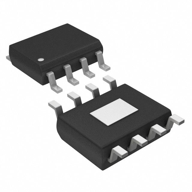
| 描述 | IC REG BUCK ADJ 5A 8SOPWRPAD稳压器—开关式稳压器 42V,5A,SD DC-DC Converter |
| DevelopmentKit | TPS54540EVM-558 |
| 产品分类 | |
| 品牌 | Texas Instruments |
| 产品手册 | http://www.ti.com/litv/slvsbx7a |
| 产品图片 |
|
| rohs | 符合RoHS无铅 / 符合限制有害物质指令(RoHS)规范要求 |
| 产品系列 | 电源管理 IC,稳压器—开关式稳压器,Texas Instruments TPS54540DDAECO-MODE™ |
| 数据手册 | |
| 产品型号 | TPS54540DDA |
| PCN设计/规格 | |
| PWM类型 | 电流模式 |
| 产品种类 | 稳压器—开关式稳压器 |
| 供应商器件封装 | 8-SO PowerPad |
| 其它名称 | 296-36231-5 |
| 包装 | 管件 |
| 同步整流器 | 无 |
| 商标 | Texas Instruments |
| 安装类型 | 表面贴装 |
| 安装风格 | SMD/SMT |
| 封装 | Tube |
| 封装/外壳 | 8-SOIC(0.154",3.90mm 宽)裸焊盘 |
| 封装/箱体 | HSOP-8 |
| 工作温度 | -40°C ~ 150°C |
| 工作温度范围 | - 40 C to + 150 C |
| 工厂包装数量 | 75 |
| 开关频率 | 100 kHz to 2.5 MHz |
| 拓扑结构 | Buck |
| 最大工作温度 | + 150 C |
| 最大输入电压 | 42 V |
| 最小工作温度 | - 40 C |
| 最小输入电压 | 4.5 V |
| 标准包装 | 75 |
| 电压-输入 | 4.5 V ~ 42 V |
| 电压-输出 | 0.8 V ~ 41.1 V |
| 电流-输出 | 5A |
| 类型 | 降压(降压) |
| 系列 | TPS54540 |
| 输出数 | 1 |
| 输出电压 | 800 mV to 41.1 V |
| 输出电流 | 5 A |
| 输出端数量 | 1 Output |
| 输出类型 | 可调式 |
| 频率-开关 | 100kHz ~ 2.5MHz |


- 商务部:美国ITC正式对集成电路等产品启动337调查
- 曝三星4nm工艺存在良率问题 高通将骁龙8 Gen1或转产台积电
- 太阳诱电将投资9.5亿元在常州建新厂生产MLCC 预计2023年完工
- 英特尔发布欧洲新工厂建设计划 深化IDM 2.0 战略
- 台积电先进制程称霸业界 有大客户加持明年业绩稳了
- 达到5530亿美元!SIA预计今年全球半导体销售额将创下新高
- 英特尔拟将自动驾驶子公司Mobileye上市 估值或超500亿美元
- 三星加码芯片和SET,合并消费电子和移动部门,撤换高东真等 CEO
- 三星电子宣布重大人事变动 还合并消费电子和移动部门
- 海关总署:前11个月进口集成电路产品价值2.52万亿元 增长14.8%


PDF Datasheet 数据手册内容提取
Product Order Technical Tools & Support & Folder Now Documents Software Community TPS54540 SLVSBX7B–MAY2013–REVISEDMARCH2017 TPS54540 4.5-V to 42-V Input, 5 A, Step Down DC-DC Converter with Eco-mode™ 1 Features 3 Description • HighEfficiencyatLightLoadswithPulseSkipping The TPS54540 is a 42 V, 5 A, step down regulator 1 with an integrated high side MOSFET. The device Eco-mode™ survives load dump pulses up to 45V per ISO 7637. • 92-mΩ High-SideMOSFET Current mode control provides simple external • 146μAOperatingQuiescentCurrentand compensation and flexible component selection. A 2μAShutdownCurrent low ripple pulse skip mode reduces the no load supply current to 146 μA. Shutdown supply current is • 100kHzto2.5MHzFixedSwitchingFrequency reducedto2μAwhentheenablepinispulledlow. • SynchronizestoExternalClock Undervoltage lockout is internally set at 4.3 V but can • LowDropoutatLightLoadswithIntegratedBOOT beincreasedusingtheenablepin.Theoutputvoltage RechargeFET start up ramp is internally controlled to provide a • AdjustableUVLOVoltageandHysteresis controlledstartupandeliminateovershoot. • 0.8V1%InternalVoltageReference A wide switching frequency range allows either • 8-TerminalHSOPwith PowerPAD™Package efficiencyorexternalcomponentsizetobeoptimized. • –40°Cto150°CT OperatingRange Output current is limited cycle-by-cycle. Frequency J foldback and thermal shutdown protects internal and • CreateaCustomDesignusingtheTPS54540with externalcomponentsduringanoverloadcondition. theWEBENCH®PowerDesigner The TPS54540 is available in an 8-terminal thermally 2 Applications enhancedHSOPPowerPAD™package. • IndustrialAutomationandMotorControl DeviceInformation • VehicleAccessories:GPS,Entertainment PARTNUMBER PACKAGE BODYSIZE • USBDedicatedChargingPortsandBattery TPS54540 HSOP(8) 4,89mmx3,9mm Chargers • 12Vand24VIndustrial,Automotiveand CommunicationsPowerSystems spacer SimplifiedSchematic EfficiencyvsLoadCurrent VIN VIN BOOT 100 36V to12V 95 TPS54540 EN SW VOUT 90 %) 85 COMP y( 12V to3.3 V nc 80 e 12V to5V ci RT/CLK FB Effi 75 70 GND 65 VOUT= 12 V, f sw = 800 kHz V = 5 V and 3.3 V, f sw = 400 kHz OUT Copyright © 2017, Texas Instruments Incorporated 60 0 0.5 1 1.5 2 2.5 3 3.5 4 4.5 5 IO-OutputCurrent(A) C024 1 An IMPORTANT NOTICE at the end of this data sheet addresses availability, warranty, changes, use in safety-critical applications, intellectualpropertymattersandotherimportantdisclaimers.PRODUCTIONDATA.
TPS54540 SLVSBX7B–MAY2013–REVISEDMARCH2017 www.ti.com Table of Contents 1 Features.................................................................. 1 7.4 DeviceFunctionalModes........................................23 2 Applications........................................................... 1 8 ApplicationandImplementation........................ 25 3 Description............................................................. 1 8.1 ApplicationInformation............................................25 4 RevisionHistory..................................................... 2 8.2 TypicalApplication..................................................25 5 PinConfigurationandFunctions......................... 4 9 PowerSupplyRecommendations...................... 36 6 Specifications......................................................... 5 10 Layout................................................................... 37 6.1 AbsoluteMaximumRatings......................................5 10.1 SafeOperatingArea.............................................37 6.2 ESDRatings..............................................................5 10.2 LayoutGuidelines.................................................38 6.3 RecommendedOperatingConditions.......................5 10.3 LayoutExample....................................................38 6.4 ThermalInformation..................................................5 11 DeviceandDocumentationSupport................. 39 6.5 ElectricalCharacteristics...........................................6 11.1 CustomDesignwithWEBENCH®Tools..............39 6.6 TimingRequirements................................................7 11.2 ReceivingNotificationofDocumentationUpdates39 6.7 TypicalCharacteristics..............................................7 11.3 CommunityResources..........................................39 7 DetailedDescription............................................ 11 11.4 Trademarks...........................................................39 7.1 Overview.................................................................11 11.5 ElectrostaticDischargeCaution............................39 7.2 FunctionalBlockDiagram.......................................12 11.6 Glossary................................................................39 7.3 FeatureDescription.................................................12 12 Mechanical,Packaging,andOrderable Information........................................................... 39 4 Revision History ChangesfromRevisionA(March2014)toRevisionB Page • AddedtheWEBENCHinformationintheFeatures,DetailedDesignProcedure,andDeviceSupportsections..................1 • ChangedtheHandlingRatingstableToESDRatingstable.................................................................................................. 5 • ChangedV MINValueFrom:4.5VTo:V +V ,andaddedNote1intheRecommendedOperatingConditions..........5 IN O DO • Deletedlastgraph:"5VStartandStopVoltage"fromtheTypicalCharacteristics............................................................. 10 • UpdatedtextandaddedEquation1intheLowDropoutOperationandBootstrapVoltage(BOOT) ................................. 13 • Deletedtext:"Thestartandstopvoltageforatypical5V..."fromtheLowDropoutOperationandBootstrapVoltage (BOOT)section..................................................................................................................................................................... 13 • ChangedEquation7andEquation8. ................................................................................................................................. 15 • ChangedEquation27 .......................................................................................................................................................... 26 • Addednewsection:MinimumV ......................................................................................................................................... 31 IN • Deleted2graphsnamed"LowDropoutOperation"fromtheApplicationCurvessection .................................................. 33 ChangesfromOriginal(May2013)toRevisionA Page • AddedDeviceInformationtable,RecommendedOperatingConditionstable,PinConfigurationandFunctions section,HandlingRatingstable,FeatureDescriptionsection,DeviceFunctionalModes,Applicationand Implementationsection,PowerSupplyRecommendationssection,Layoutsection,DeviceandDocumentation Supportsection,andMechanical,Packaging,andOrderableInformationsection................................................................ 1 • ChangedtheElectricalCharacteristicsConditionsFrom:VIN=4.5to60VTo:VIN=4.5to42V...................................... 6 • ChangedtheOperating:nonswitchingsupplycurrentTESTCONDITIONSFrom:FB=0.83VTo:FB=0.9V.................. 6 • ChangedRT/CLKhighthresholdMAXvalueFrom:1.7VTo:2V ....................................................................................... 6 • Changedthetitleofgraph"5VStartandStopVoltage"toincludealinktotheLowDropoutOperationsection. ............10 • ChangedtheFBD,removedtheLogicblockandShutdownsignalfromtheOVcomparator............................................. 12 • ChangedVF=ForwardDropoftheCatchDiodeTo:V =ForwardDropoftheCatchDiode .......................................... 14 D • DeletedvalueTSW=1/FswfromthelistfollowingEquation2......................................................................................... 14 • ChangedVB2SW=VBOOT+VFTo:VB2SW=VBOOT+V ........................................................................................... 14 D • ChangedVBOOT=(1.41xV -0.554-VF/TSW-1.847x103xIB2SW)/(1.41+1/Tsw)To:VBOOT=(1.41x IN 2 SubmitDocumentationFeedback Copyright©2013–2017,TexasInstrumentsIncorporated ProductFolderLinks:TPS54540
TPS54540 www.ti.com SLVSBX7B–MAY2013–REVISEDMARCH2017 V -0.554-V xƒ -1.847x10³xIB2SW)/(1.41+ƒ )............................................................................................... 14 IN D SW SW • Deletedfigure:"5VStart/StopVoltage"................................................................................................................................ 14 • AddedatitletoFigure23..................................................................................................................................................... 14 • ChangedthesectiontitleFrom:SelectingtheSwitchingFrequencyTo:AccurateCurrentLimitOperationand MaximumSwitchingFrequency............................................................................................................................................ 16 • ChangedtextintheSynchronizationtoRT/CLKterminalsectionFrom:"0.5Vandhigherthan1.7V"To:"0.5Vand higherthan2V" ................................................................................................................................................................... 17 • ChangedEquation33From:(5.13V2-5V2)To:3.43V2-3.3V2)...................................................................................... 28 • ChangedFigure36,VOUTFrom:200mV/divTo100mV/div ............................................................................................ 33 • ChangedFigure38,ENFrom:1V/divTo:2V/div,VOUTFrom:4V/divTo:2V/div,andTime=2ms/divTo:Time =20ms/div........................................................................................................................................................................... 33 • ChangedFigure39,VOUTFrom:4V/divTo:2V/div......................................................................................................... 33 Copyright©2013–2017,TexasInstrumentsIncorporated SubmitDocumentationFeedback 3 ProductFolderLinks:TPS54540
TPS54540 SLVSBX7B–MAY2013–REVISEDMARCH2017 www.ti.com 5 Pin Configuration and Functions HSOICPackage (TopView) BOOT 1 8 SW VIN 2 7 GND PowerPAD 9 EN 3 6 COMP RT/CLK 4 5 FB PinFunctions TERMINAL I/O DESCRIPTION NAME NO. AbootstrapcapacitorisrequiredbetweenBOOTandSW.Ifthevoltageonthiscapacitorisbelowtheminimum BOOT 1 O requiredtooperatethehighsideMOSFET,theoutputisswitchedoffuntilthecapacitorisrefreshed. VIN 2 I Inputsupplyvoltagewith4.5Vto42Voperatingrange. Enableterminal,withinternalpull-upcurrentsource.Pullbelow1.2Vtodisable.Floattoenable.Adjustthe EN 3 I inputundervoltagelockoutwithtworesistors.SeetheEnableandAdjustingUndervoltageLockoutsection. ResistorTimingandExternalClock.Aninternalamplifierholdsthisterminalatafixedvoltagewhenusingan externalresistortogroundtosettheswitchingfrequency.IftheterminalispulledabovethePLLupper RT/CLK 4 I threshold,amodechangeoccursandtheterminalbecomesasynchronizationinput.Theinternalamplifieris disabledandtheterminalisahighimpedanceclockinputtotheinternalPLL.Ifclockingedgesstop,the internalamplifierisre-enabledandtheoperatingmodereturnstoresistorfrequencyprogramming. FB 5 I Invertinginputofthetransconductance(gm)erroramplifier. Erroramplifieroutputandinputtotheoutputswitchcurrent(PWM)comparator.Connectfrequency COMP 6 O compensationcomponentstothisterminal. GND 7 – Ground SW 8 I Thesourceoftheinternalhigh-sidepowerMOSFETandswitchingnodeoftheconverter. Thermal GNDterminalmustbeelectricallyconnectedtotheexposedpadontheprintedcircuitboardforproper 9 – Pad operation. 4 SubmitDocumentationFeedback Copyright©2013–2017,TexasInstrumentsIncorporated ProductFolderLinks:TPS54540
TPS54540 www.ti.com SLVSBX7B–MAY2013–REVISEDMARCH2017 6 Specifications 6.1 Absolute Maximum Ratings(1) overoperatingfree-airtemperaturerange(unlessotherwisenoted) VALUE UNIT MIN MAX VIN –0.3 45 EN –0.3 8.4 BOOT 53 Inputvoltage V FB –0.3 3 COMP –0.3 3 RT/CLK –0.3 3.6 BOOT-SW 8 Outputvoltage SW –0.6 45 V SW,10-nsTransient –2 45 Operatingjunctiontemperature,T –40 150 °C J Storagetemperature,T –65 150 °C STG (1) Stressesbeyondthoselistedunderabsolutemaximumratingsmaycausepermanentdamagetothedevice.Thesearestressratings onlyandfunctionaloperationofthedeviceattheseoranyotherconditionsbeyondthoseindicatedunderrecommendedoperating conditionsisnotimplied.Exposuretoabsolute-maximum-ratedconditionsforextendedperiodsmayaffectdevicereliability. 6.2 ESD Ratings VALUE UNIT HumanBodyModel(HBM)ESDStressVoltage (2) ±2000 V V (1) ESD ChargedDeviceModel(HBM)ESDStressVoltage (3) ±500 V (1) Electrostaticdischarge(ESD)tomeasuredevicesensitivityandimmunitytodamagecausedbyassemblylineelectrostaticdischarges intothedevice. (2) LevellistedaboveisthepassinglevelperANSI/ESDA/JEDECJS-001.JEDECdocumentJEP155statesthat500VHBMallowssafe manufacturingwithastandardESDcontrolprocess.terminalslistedas1000Vmayactuallyhavehigherperformance. (3) LevellistedaboveisthepassinglevelperEIA-JEDECJESD22-C101.JEDECdocumentJEP157statesthat250VCDMallowssafe manufacturingwithastandardESDcontrolprocess.terminalslistedas250Vmayactuallyhavehigherperformance. 6.3 Recommended Operating Conditions overoperatingfree-airtemperaturerange(unlessotherwisenoted) MIN MAX UNIT VIN Supplyinputvoltage(1) VO+VDO 42 V VO Outputvoltage 0.8 41.1 V IO Outputcurrent 0 5 A TJ JunctionTemperature –40 150 °C (1) SeeEquation1 6.4 Thermal Information TPS54540 THERMALMETRIC(1)(2) UNIT DDA(8PINS) θJA Junction-to-ambientthermalresistance(standardboard) 42.0 °C/W ψJT Junction-to-topcharacterizationparameter 5.9 °C/W ψJB Junction-to-boardcharacterizationparameter 23.4 °C/W θJCtop Junction-to-case(top)thermalresistance 45.8 °C/W θJCbot Junction-to-case(bottom)thermalresistance 3.6 °C/W θJB Junction-to-boardthermalresistance 23.4 v (1) Formoreinformationabouttraditionalandnewthermalmetrics,seetheICPackageThermalMetricsapplicationreport,SPRA953. (2) PowerratingataspecificambienttemperatureTAshouldbedeterminedwithajunctiontemperatureof150°C.Thisisthepointwhere distortionstartstosubstantiallyincrease.Seepowerdissipationestimateinapplicationsectionofthisdatasheetformoreinformation. Copyright©2013–2017,TexasInstrumentsIncorporated SubmitDocumentationFeedback 5 ProductFolderLinks:TPS54540
TPS54540 SLVSBX7B–MAY2013–REVISEDMARCH2017 www.ti.com 6.5 Electrical Characteristics T =–40°Cto150°C,VIN=4.5to42V(unlessotherwisenoted) J PARAMETER TESTCONDITIONS MIN TYP MAX UNIT SUPPLYVOLTAGE(VINTERMINAL) Operatinginputvoltage 4.5 42 V Internalundervoltagelockoutthreshold Rising 4.1 4.3 4.48 V Internalundervoltagelockoutthreshold 325 mV hysteresis Shutdownsupplycurrent EN=0V,25°C,4.5V≤VIN≤42V 2.25 4.5 μA Operating:nonswitchingsupplycurrent FB=0.9V,TA=25°C 146 175 ENABLEANDUVLO(ENTERMINAL) Enablethresholdvoltage Novoltagehysteresis,risingandfalling 1.1 1.2 1.3 V Enablethreshold+50mV –4.6 Inputcurrent μA Enablethreshold–50mV –0.58 –1.2 –1.8 Hysteresiscurrent –2.2 –3.4 –4.5 μA VOLTAGEREFERENCE Voltagereference 0.792 0.8 0.808 V HIGH-SIDEMOSFET On-resistance VIN=12V,BOOT-SW=6V 92 190 mΩ ERRORAMPLIFIER Inputcurrent 50 nA Erroramplifiertransconductance(gM) –2μA<ICOMP<2μA,VCOMP=1V 350 μMhos Esorrfot-rstaamrtplifiertransconductance(gM)during –2μA<ICOMP<2μA,VCOMP=1V,VFB=0.4V 77 μMhos Erroramplifierdcgain VFB=0.8V 10,000 V/V Minunitygainbandwidth 2500 kHz Erroramplifiersource/sink V(COMP)=1V,100mVoverdrive ±30 μA COMPtoSWcurrenttransconductance 17 A/V CURRENTLIMIT AllVINandtemperatures,OpenLoop(1) 6.3 7.5 8.8 Currentlimitthreshold Alltemperatures,VIN=12V,OpenLoop(1) 6.3 7.5 8.3 A VIN=12V,TA=25°C,OpenLoop(1) 7.1 7.5 7.9 THERMALSHUTDOWN Thermalshutdown 176 °C Thermalshutdownhysteresis 12 °C TIMINGRESISTORANDEXTERNALCLOCK(RT/CLKTERMINAL) SwitchingfrequencyrangeusingRTmode 100 2500 kHz fSW Switchingfrequency RT=200kΩ 450 500 550 kHz SwitchingfrequencyrangeusingCLKmode 160 2300 kHz RT/CLKhighthreshold 1.55 2 V RT/CLKlowthreshold 0.5 1.2 V (1) OpenLoopcurrentlimitmeasureddirectlyattheSWterminalandisindependentoftheinductorvalueandslopecompensation. 6 SubmitDocumentationFeedback Copyright©2013–2017,TexasInstrumentsIncorporated ProductFolderLinks:TPS54540
TPS54540 www.ti.com SLVSBX7B–MAY2013–REVISEDMARCH2017 6.6 Timing Requirements PARAMETER TESTCONDITIONS MIN TYP MAX UNIT ENABLEANDUVLO(ENTERMINAL) EnabletoCOMPactive VIN=12V,TA=25°C 540 µs INTERNALSOFT-STARTTIME Soft-StartTime fSW=500kHz,10%to90% 2.1 ms Soft-StartTime fSW=2.5MHz,10%to90% 0.42 ms HIGH-SIDEMOSFET On-resistance VIN=12V,BOOT-SW=6V 92 190 mΩ TIMINGRESISTORANDEXTERNALCLOCK(RT/CLKTERMINAL) MinimumCLKinputpulsewidth 15 ns RT/CLKfallingedgetoSWrisingedge Measuredat500kHzwithRTresistorinseries 55 ns delay PLLlockintime Measuredat500kHz 78 μs 6.7 Typical Characteristics 0.25 0.814 (cid:13)nce () 0.2 e ( V) 0.809 esista 0.15 eranc 0.804 R ef e R 0.799 at e On-St 0.1 Voltag 0.794 - DSON0.05 BOOT-SW = 3 V V - FB0.789 R BOOT-SW = 6 V 0 0.784 –50 –25 0 25 50 75 100 125 150 –50 –25 0 25 50 75 100 125 150 TJ - Junction Temperature ((cid:131)C) C025 TJ - Junction Temperature ((cid:131)C) C026 Figure1.OnResistancevsJunctionTemperature Figure2.VoltageReferencevsJunctionTemperature 9 9 –S4e0ri e(cid:131)Cs1 2S5e r(cid:131)iCes 2 urrent (A) 8.85 Current (A) 8.58 1S5e0ri e(cid:131)Cs4 witch C 7.5 Switch 7.5 e S de 7 h Sid 7 gh Si g Hi 6.5 Hi 6.5 6 6 0 7 14 21 28 35 42 -50 -25 0TJ - Ju2n5ction T5e0mpera7tu5re (qC10)0 125 150 VI - Input Voltage (V) C028 Figure4.SwitchCurrentLimitvsInputVoltage Figure3.SwitchCurrentLimitvsJunctionTemperature Copyright©2013–2017,TexasInstrumentsIncorporated SubmitDocumentationFeedback 7 ProductFolderLinks:TPS54540
TPS54540 SLVSBX7B–MAY2013–REVISEDMARCH2017 www.ti.com Typical Characteristics (continued) 550 500 F - Switching Frequency (kHz) S444455555678901234000000000 F - Switching Frequency (kHz) SW11223344050505055000000000 450 0 –50 –25 0 25 50 75 100 125 150 200 300 400 500 600 700 800 900 1000 TJ - Junction Temperature ((cid:131)C) C029 RT/CLK - Resistance (k(cid:13)) C030 Figure5.SwitchingFrequencyvsJunctionTemperature Figure6.SwitchingFrequencyvsRT/CLKResistance LowFrequencyRange 2500 500 z) 2300 H 450 k 2100 y ( c 1900 n 400 e qu 1700 V) Fre 1500 µA/ 350 hing 1300 gm ( witc 1100 300 S - W 900 250 S F 700 500 200 0 50 100 150 200 –50 –25 0 25 50 75 100 125 150 RT/CLK - Resistance (k(cid:13)) C031 TJ - Junction Temperature ((cid:131)C) C032 Figure7.SwitchingFrequencyvsRT/CLKResistance Figure8.EATransconductancevsJunctionTemperature HighFrequencyRange 120 1.3 1.29 110 1.28 100 1.27 V) 8900 old (V) 111...222456 gm (µA/ 567000 EN - Thresh 1111....11222.91232 40 1.18 1.17 30 1.16 20 1.15 –50 –25 0 25 50 75 100 125 150 –50 –25 0 25 50 75 100 125 150 TJ - Junction Temperature ((cid:131)C) C033 TJ - Junction Temperature ((cid:131)C) C034 Figure9.EATransconductanceDuringSoft-Startvs Figure10.ENTerminalVoltagevsJunctionTemperature JunctionTemperature 8 SubmitDocumentationFeedback Copyright©2013–2017,TexasInstrumentsIncorporated ProductFolderLinks:TPS54540
TPS54540 www.ti.com SLVSBX7B–MAY2013–REVISEDMARCH2017 Typical Characteristics (continued) –3.5 –0.5 –3.7 –0.7 –3.9 –0.9 –4.1 –1.1 A) –4.3 A) –1.3 (uN–4.5 (µN–1.5 IE–4.7 IE–1.7 –4.9 –1.9 –5.1 –2.1 –5.3 –2.3 –5.5 –2.5 –50 –25 0 25 50 75 100 125 150 –50 –25 0 25 50 75 100 125 150 TJ - Junction Temperature ((cid:131)C) C035 TJ - Junction Temperature ((cid:131)C) C036 Figure11.ENTerminalCurrentvsJunctionTemperature Figure12.ENTerminalCurrentvsJunctionTemperature –2.5 100 VSerie Fsa2l ling –2.7 y SENSE –2.9 uenc VSSENeSrEie Rs4is ing µA) –3.1 Freq 75 s ( –3.3 ng I - HysteresiEN–––333...975 ominal Switchi 2550 –4.1 N of –4.3 % –4.5 0 –50 –25 0 25 50 75 100 125 150 0.0 0.1 0.2 0.3 0.4 0.5 0.6 0.7 0.8 TJ - Junction Temperature ((cid:131)C) C037 VSENSE (V) C038 Figure13.ENTerminalCurrentHysteresisvsJunction Figure14.SwitchingFrequencyvsV SENSE Temperature 3 3 T =S 2e5ri(cid:131)eCs2 J 2.5 2.5 2 2 A) A) (µN1.5 (µN1.5 IVI IVI 1 1 0.5 0.5 0 0 –50 –25 0 25 50 75 100 125 150 0 7 14 21 28 35 42 TJ - Junction Temperature ((cid:131)C) C039 VIN - Input Voltage (V) C040 Figure15.ShutdownSupplyCurrentvsJunction Figure16.ShutdownSupplyCurrentvsInputVoltage(V ) IN Temperature Copyright©2013–2017,TexasInstrumentsIncorporated SubmitDocumentationFeedback 9 ProductFolderLinks:TPS54540
TPS54540 SLVSBX7B–MAY2013–REVISEDMARCH2017 www.ti.com Typical Characteristics (continued) 210 210 TS =e r2ie5s(cid:131)C2 J 190 190 170 170 A) 150 A) 150 µ µ (N (N IVI130 IVI130 110 110 90 90 70 70 –50 –25 0 25 50 75 100 125 150 0 7 14 21 28 35 42 TJ - Junction Temperature ((cid:131)C) C041 VIN - Input Voltage (V) C042 Figure17.V SupplyCurrentvsJunctionTemperature Figure18.V SupplyCurrentvsInputVoltage IN IN 2.6 4.5 BOOT-PH UVLO Falling UVLO Start Switching 2.5 BOOT-PH UVLO Rising 4.4 UVLO Stop Switching 2.4 4.3 V) H ( 2.3 4.2 OT-P 2.2 (V) N4.1 O VI V - BI2.1 4.0 2.0 3.9 1.9 3.8 1.8 3.7 –50 –25 0 25 50 75 100 125 150 –50 –25 0 25 50 75 100 125 150 TJ - Junction Temperature ((cid:131)C) C043 TJ - Junction Temperature ((cid:131)C) C044 Figure19.BOOT-SWUVLOvsJunctionTemperature Figure20.InputVoltageUVLOvsJunctionTemperature 10 1122 V V, ,2 255(cid:131)C C 9 8 ms) 7 e ( 6 m Ti 5 art St 4 oft- 3 S 2 1 0 110000 3 03000 5 0 500 0 7 0700 0 9 09000 1 11 01000 1 3 1 0 300 10 5 1 0 5000 1 7 10 700 10 9 10 900 20 1 20 100 20 3 20 300 20 5 20 500 0 Switching Frequency (kHz) C045 Figure21.Soft-StartTimevsSwitchingFrequency 10 SubmitDocumentationFeedback Copyright©2013–2017,TexasInstrumentsIncorporated ProductFolderLinks:TPS54540
TPS54540 www.ti.com SLVSBX7B–MAY2013–REVISEDMARCH2017 7 Detailed Description 7.1 Overview The TPS54540 is a 42 V, 5 A, step-down (buck) regulator with an integrated high side n-channel MOSFET. The device implements constant frequency, current mode control which reduces output capacitance and simplifies external frequency compensation. The wide switching frequency range of 100 kHz to 2500 kHz allows either efficiency or size optimization when selecting the output filter components. The switching frequency is adjusted usingaresistortogroundconnectedtotheRT/CLKterminal.Thedevicehasaninternalphase-lockedloop(PLL) connected to the RT/CLK terminal that will synchronize the power switch turn on to a falling edge of an external clocksignal. The TPS54540 has a default input start-up voltage of approximately 4.3 V. The EN terminal can be used to adjust the input voltage undervoltage lockout (UVLO) threshold with two external resistors. An internal pull up currentsourceenablesoperationwhentheENterminalisfloating.Theoperatingcurrentis146 μAundernoload condition(notswitching).Whenthedeviceisdisabled,thesupplycurrentis2 μA. The integrated 92 mΩ high side MOSFET supports high efficiency power supply designs capable of delivering 5 amperes of continuous current to a load. The gate drive bias voltage for the integrated high side MOSFET is supplied by a bootstrap capacitor connected from the BOOT to SW terminals. The TPS54540 reduces the external component count by integrating the bootstrap recharge diode. The BOOT terminal capacitor voltage is monitored by a UVLO circuit which turns off the high side MOSFET when the BOOT to SW voltage falls below a preset threshold. An automatic BOOT capacitor recharge circuit allows the TPS54540 to operate at high duty cycles approaching 100%. Therefore, the maximum output voltage is near the minimum input supply voltage of theapplication.Theminimumoutputvoltageistheinternal0.8Vfeedbackreference. Output overvoltage transients are minimized by an Overvoltage Transient Protection (OVP) comparator. When the OVP comparator is activated, the high side MOSFET is turned off and remains off until the output voltage is lessthan106%ofthedesiredoutputvoltage. The TPS54540 includes an internal soft-start circuit that slows the output rise time during start-up to reduce in- rush current and output voltage overshoot. Output overload conditions reset the soft-start timer. When the overloadconditionisremoved,thesoft-startcircuitcontrolstherecoveryfromthefaultoutputleveltothenominal regulation voltage. A frequency foldback circuit reduces the switching frequency during start-up and overcurrent faultconditionstohelpmaintaincontroloftheinductorcurrent. Copyright©2013–2017,TexasInstrumentsIncorporated SubmitDocumentationFeedback 11 ProductFolderLinks:TPS54540
TPS54540 SLVSBX7B–MAY2013–REVISEDMARCH2017 www.ti.com 7.2 Functional Block Diagram EN VIN Thermal Shutdown UVLO Enable OV Comparator Shutdown Shutdown Logic Enable Threshold Boot Charge Voltage Minimum Boot Reference Clamp UVLO CSuernresnet Pulse Error S kip Amplifier PWM FB Comparator BOOT Logic Shutdown 6 Slope Compensation COMP SW Frequency Foldback Reference DAC for Soft-Start Maximum Clamp Oscillator with PLL 8/8/ 2012 A 0192789 GND POWERPAD RT/CLK Copyright ' 2016, Texas Instruments Incorporated 7.3 Feature Description 7.3.1 FixedFrequencyPWMControl The TPS54540 uses fixed frequency, peak current mode control with adjustable switching frequency. The output voltage is compared through external resistors connected to the FB terminal to an internal voltage reference by an error amplifier. An internal oscillator initiates the turn on of the high side power switch. The error amplifier output at the COMP terminal controls the high side power switch current. When the high side MOSFET switch current reaches the threshold level set by the COMP voltage, the power switch is turned off. The COMP terminal voltage will increase and decrease as the output current increases and decreases. The device implements current limiting by clamping the COMP terminal voltage to a maximum level. The pulse skipping Eco-mode is implementedwithaminimumvoltageclampontheCOMPterminal. 7.3.2 SlopeCompensationOutputCurrent The TPS54540 adds a compensating ramp to the MOSFET switch current sense signal. This slope compensation prevents sub-harmonic oscillations at duty cycles greater than 50%. The peak current limit of the highsideswitchisnotaffectedbytheslopecompensationandremainsconstantoverthefulldutycyclerange. 12 SubmitDocumentationFeedback Copyright©2013–2017,TexasInstrumentsIncorporated ProductFolderLinks:TPS54540
TPS54540 www.ti.com SLVSBX7B–MAY2013–REVISEDMARCH2017 Feature Description (continued) 7.3.3 PulseSkipEco-mode The TPS54540 operates in a pulse skipping Eco-mode at light load currents to improve efficiency by reducing switching and gate drive losses. If the output voltage is within regulation and the peak switch current at the end of any switching cycle is below the pulse skipping current threshold, the device enters Eco-mode. The pulse skippingcurrentthresholdisthepeakswitchcurrentlevelcorrespondingtoanominalCOMPvoltageof600mV. When in Eco-mode, the COMP terminal voltage is clamped at 600 mV and the high side MOSFET is inhibited. Since the device is not switching, the output voltage begins to decay. The voltage control loop responds to the falling output voltage by increasing the COMP terminal voltage. The high side MOSFET is enabled and switching resumes when the error amplifier lifts COMP above the pulse skipping threshold. The output voltage recovers to the regulated value, and COMP eventually falls below the Eco-mode pulse skipping threshold at which time the device again enters Eco-mode. The internal PLL remains operational when in Eco-mode. When operating at light loadcurrentsinEco-mode,theswitchingtransitionsoccursynchronouslywiththeexternalclocksignal. During Eco-mode operation, the TPS54540 senses and controls peak switch current, not the average load current. Therefore the load current at which the device enters Eco-mode is dependent on the output inductor value. The circuit in Figure 35 enters Eco-mode at about 18 mA output current. As the load current approaches zero,thedeviceentersapulseskipmodeduringwhichitdrawsonly146 μAinputquiescentcurrent. 7.3.4 LowDropoutOperationandBootstrapVoltage(BOOT) The TPS54540 provides an integrated bootstrap voltage regulator. A small capacitor between the BOOT and SW terminals provides the gate drive voltage for the high side MOSFET. The BOOT capacitor is refreshed when the high side MOSFET is off and the external low side diode conducts. The recommended value of the BOOT capacitor is 0.1 μF. A ceramic capacitor with an X7R or X5R grade dielectric with a voltage rating of 10 V or higherisrecommendedforstableperformanceovertemperatureandvoltage. When operating with a low voltage difference from input to output, the high side MOSFET of the TPS54540 will operate at 100% duty cycle as long as the BOOT to SW terminal voltage is greater than 2.1V. When the voltage from BOOT to SW drops below 2.1V, the high side MOSFET is turned off and an integrated low side MOSFET pulls SW low to recharge the BOOT capacitor. To reduce the losses of the small low side MOSFET at high outputvoltages,itisdisabledat24Voutputandre-enabledwhentheoutputreaches21.5V. SincethegatedrivecurrentsourcedfromtheBOOTcapacitorissmall,thehighsideMOSFETcanremainonfor many switching cycles before the MOSFET is turned off to refresh the capacitor. Thus the effective duty cycle of the switching regulator can be high, approaching 100%. The effective duty cycle of the converter during dropout is mainly influenced by the voltage drops across the power MOSFET, the inductor resistance, the low side diode voltageandtheprintedcircuitboardresistance. Equation 1 calculates the minimum input voltage required to regulate the output voltage and ensure normal operation of the device. This calculation must include tolerance of the component specifications and the variation ofthesespecificationsattheirmaximumoperatingtemperatureintheapplication V (cid:14)V (cid:14)R uI V (cid:11)min(cid:12) OUT F dc OUT (cid:14)R uI (cid:16)V IN 0.99 DS(cid:11)on(cid:12) OUT F where • V =Schottkydiodeforwardvoltage F • R =DCresistanceofinductorandPCB dc • R =High-sideMOSFETR (1) DS(on) DS(on) During high duty cycle (low dropout) conditions, inductor current ripple increases when the BOOT capacitor is being recharged resulting in an increase in output voltage ripple. Increased ripple occurs when the off time required to recharge the BOOT capacitor is longer than the high side off time associated with cycle by cycle PWMcontrol. At heavy loads, the minimum input voltage must be increased to insure a monotonic startup. Equation 2 can be usedtocalculatetheminimuminputvoltageforthiscondition. Copyright©2013–2017,TexasInstrumentsIncorporated SubmitDocumentationFeedback 13 ProductFolderLinks:TPS54540
TPS54540 SLVSBX7B–MAY2013–REVISEDMARCH2017 www.ti.com Feature Description (continued) V =D x(V -I xR +V )-V +I xR OUT(max) (max) IN(min) OUT(max) DS(on) D D OUT(max) dc where • D ≥0.9 (max) • IB2SW=100µA • V =ForwardDropoftheCatchDiode D • VB2SW=VBOOT+V D • VBOOT=(1.41xV -0.554-V xf -1.847x10³xIB2SW)/(1.41+f ) IN D SW SW • R =1/(-0.3xVB2SW2+3.577xVB2SW-4.246) (2) DS(on) 7.3.5 ErrorAmplifier The TPS54540 voltage regulation loop is controlled by a transconductance error amplifier. The error amplifier compares the FB terminal voltage to the lower of the internal soft-start voltage or the internal 0.8 V voltage reference. The transconductance (gm) of the error amplifier is 350 μA/V during normal operation. During soft- start operation, the transconductance is reduced to 78 μA/V and the error amplifier is referenced to the internal soft-startvoltage. The frequency compensation components (capacitor, series resistor and capacitor) are connected between the erroramplifieroutputCOMPterminalandGNDterminal. 7.3.6 AdjustingtheOutputVoltage The internal voltage reference produces a precise 0.8 V ±1% voltage reference over the operating temperature and voltage range by scaling the output of a bandgap reference circuit. The output voltage is set by a resistor divider from the output node to the FB terminal. It is recommended to use 1% tolerance or better divider resistors. Select the low side resistor R for the desired divider current and use Equation 3 to calculate R . To LS HS improve efficiency at light loads consider using larger value resistors. However, if the values are too high, the regulatorwillbemoresusceptibletonoiseandvoltageerrorsfromtheFBinputcurrentmaybecomenoticeable. æVout - 0.8Vö RHS =RLS ´ ç ÷ è 0.8V ø (3) 7.3.7 EnableandAdjustingUndervoltageLockout The TPS54540 is enabled when the VIN terminal voltage rises above 4.3 V and the EN terminal voltage exceeds the enable threshold of 1.2 V. The TPS54540 is disabled when the VIN terminal voltage falls below 4 V or when the EN terminal voltage is below 1.2 V. The EN terminal has an internal pull-up current source, I1, of 1.2 μA that enablesoperationoftheTPS54540whentheENterminalfloats. If an application requires a higher undervoltage lockout (UVLO) threshold, use the circuit shown in Figure 22 to adjust the input voltage UVLO with two external resistors. When the EN terminal voltage exceeds 1.2 V, an additional 3.4 μA of hysteresis current, I , is sourced out of the EN terminal. When the EN terminal is pulled HYS below 1.2 V, the 3.4 μA Ihys current is removed. This additional current facilitates adjustable input voltage UVLO hysteresis. Use Equation 4 to calculate R for the desired UVLO hysteresis voltage. Use Equation 5 to UVLO1 calculateR forthedesiredVINstartvoltage. UVLO2 In applications designed to start at relatively low input voltages (that is, from 4.5 V to 9 V) and withstand high input voltages (that is, up to 42 V), the EN terminal may experience a voltage greater than the absolute maximum voltage of 8.4 V during the high input voltage condition. To avoid exceeding this voltage when using theENresistors,theENterminalisclampedinternallywitha5.8Vzenerdiodethatwillsinkupto150 μA. 14 SubmitDocumentationFeedback Copyright©2013–2017,TexasInstrumentsIncorporated ProductFolderLinks:TPS54540
TPS54540 www.ti.com SLVSBX7B–MAY2013–REVISEDMARCH2017 Feature Description (continued) VIN TPS54540 VIN i1 ihys RUVLO1 RUVLO1 10 kW EN EN Node VEN RUVLO2 RUVLO2 5.8 V Copyright © 2017,Texas Instruments Incorporated Copyright © 2016,Texas Instruments Incorporated Figure22.AdjustableUndervoltageLockout Figure23.InternalENTerminalClamp (UVLO) V -V R = START STOP UVLO1 I HYS (4) V R = ENA UVLO2 V -V START ENA +I R 1 UVLO1 (5) 7.3.8 InternalSoft-Start The TPS54540 has an internal digital soft-start that ramps the reference voltage from zero volts to its final value in1024switchingcycles.Theinternalsoft-starttime(10%to90%)iscalculatedusingEquation6. 1024 t (ms)= SS f (kHz) SW (6) If the EN terminal is pulled below the stop threshold of 1.2 V, switching stops and the internal soft-start resets. Thesoft-startalsoresetsinthermalshutdown. 7.3.9 ConstantSwitchingFrequencyandTimingResistor(RT/CLK)Terminal) The switching frequency of the TPS54540 is adjustable over a wide range from 100 kHz to 2500 kHz by placing a resistor between the RT/CLK terminal and GND terminal. The RT/CLK terminal voltage is typically 0.5 V and must have a resistor to ground to set the switching frequency. To determine the timing resistance for a given switching frequency, use Equation 7 or Equation 8or the curves in Figure 5 and Figure 6. To reduce the solution size one would typically set the switching frequency as high as possible, but tradeoffs of the conversion efficiency, maximum input voltage and minimum controllable on time should be considered. The minimum controllable on time is typically 135 ns which limits the maximum operating frequency in applications with high input to output step down ratios. The maximum switching frequency is also limited by the frequency foldback circuit.Amoredetaileddiscussionofthemaximumswitchingfrequencyisprovidedinthenextsection. 101756 R (kW)= T fsw(kHz)1.008 (7) 92417 fsw(kHz)= RT(kW)0.991 (8) Copyright©2013–2017,TexasInstrumentsIncorporated SubmitDocumentationFeedback 15 ProductFolderLinks:TPS54540
TPS54540 SLVSBX7B–MAY2013–REVISEDMARCH2017 www.ti.com Feature Description (continued) 7.3.10 AccurateCurrentLimitOperationandMaximumSwitchingFrequency The TPS54540 implements peak current mode control in which the COMP terminal voltage controls the peak current of the high side MOSFET. A signal proportional to the high side switch current and the COMP terminal voltage are compared each cycle. When the peak switch current intersects the COMP control voltage, the high side switch is turned off. During overcurrent conditions that pull the output voltage low, the error amplifier increases switch current by driving the COMP terminal high. The error amplifier output is clamped internally at a level which sets the peak switch current limit. The TPS54540 provides an accurate current limit threshold with a typical current limit delay of 60 ns. With smaller inductor values, the delay will result in a higher peak inductor current.TherelationshipbetweentheinductorvalueandthepeakinductorcurrentisshowninFigure24. Peak Inductor Current Δ ) CLPeak Open Loop Current Limit A ( nt e r r u C r o ct u d n I Δ = V /Lx t CLPeak IN CLdelay t CLdelay t ON Figure24. CurrentLimitDelay To protect the converter in overload conditions at higher switching frequencies and input voltages, the TPS54540 implements a frequency foldback. The oscillator frequency is divided by 1, 2, 4, and 8 as the FB terminal voltage falls from 0.8 V to 0 V. The TPS54540 uses a digital frequency foldback to enable synchronization to an external clock during normal start-up and fault conditions. During short-circuit events, the inductor current can exceed the peak current limit because of the high input voltage and the minimum controllable on time. When the output voltage is forced low by the shorted load, the inductor current decreases slowly during the switch off time. The frequency foldback effectively increases the off time by increasing the period of the switching cycle providing moretimefortheinductorcurrenttorampdown. With a maximum frequency foldback ratio of 8, there is a maximum frequency at which the inductor current can be controlled by frequency foldback protection. Equation 10 calculates the maximum switching frequency at which the inductor current will remain under control when V is forced to V . The selected operating OUT OUT(SC) frequencyshouldnotexceedthecalculatedvalue. Equation 9 calculates the maximum switching frequency limitation set by the minimum controllable on time and the input to output step down ratio. Setting the switching frequency above this value will cause the regulator to skipswitchingpulsestoachievethelowdutycyclerequiredatmaximuminputvoltage. æ ö 1 I ´R +V +V f = ´ç O dc OUT d ÷ SW(maxskip) t çV -I ´R +V ÷ ON è IN O DS(on) d ø (9) 16 SubmitDocumentationFeedback Copyright©2013–2017,TexasInstrumentsIncorporated ProductFolderLinks:TPS54540
TPS54540 www.ti.com SLVSBX7B–MAY2013–REVISEDMARCH2017 Feature Description (continued) æI ´R +V +V ö f = fDIV ´ç CL dc OUT(sc) d ÷ SW(shift) t ç V -I ´R +V ÷ ON è IN CL DS(on) d ø (10) I Outputcurrent O I Currentlimit CL Rdc inductorresistance V maximuminputvoltage IN V outputvoltage OUT V outputvoltageduringshort OUTSC Vd diodevoltagedrop R switchonresistance DS(on) t controllableontime ON ƒ frequencydivideequals(1,2,4,or8) DIV 7.3.11 SynchronizationtoRT/CLKTerminal The RT/CLK terminal can receive a frequency synchronization signal from an external system clock. To implement this synchronization feature connect a square wave to the RT/CLK terminal through either circuit network shown in Figure 25. The square wave applied to the RT/CLK terminal must switch lower than 0.5 V and higher than 2 V and have a pulsewidth greater than 15 ns. The synchronization frequency range is 160 kHz to 2300 kHz. The rising edge of the SW will be synchronized to the falling edge of RT/CLK terminal signal. The external synchronization circuit should be designed such that the default frequency set resistor is connected from the RT/CLK terminal to ground when the synchronization signal is off. When using a low impedance signal source, the frequency set resistor is connected in parallel with an ac coupling capacitor to a termination resistor (that is, 50 Ω) as shown in Figure 25. The two resistors in series provide the default frequency setting resistance when the signal source is turned off. The sum of the resistance should set the switching frequency close to the external CLK frequency. It is recommended to ac couple the synchronization signal through a 10 pF ceramic capacitortoRT/CLKterminal. The first time the RT/CLK is pulled above the PLL threshold the TPS54540 switches from the RT resistor free- running frequency mode to the PLL synchronized mode. The internal 0.5 V voltage source is removed and the RT/CLK terminal becomes high impedance as the PLL starts to lock onto the external signal. The switching frequency can be higher or lower than the frequency set with the RT/CLK resistor. The device transitions from the resistor mode to the PLL mode and locks onto the external clock frequency within 78 microseconds. During the transition from the PLL mode to the resistor programmed mode, the switching frequency will fall to 150 kHz and then increase or decrease to the resistor programmed frequency when the 0.5 V bias voltage is reapplied to theRT/CLKresistor. The switching frequency is divided by 8, 4, 2, and 1 as the FB terminal voltage ramps from 0 to 0.8 volts. The device implements a digital frequency foldback to enable synchronizing to an external clock during normal start- up and fault conditions. Figure 26, Figure 27 and Figure 28 show the device synchronized to an external system clockincontinuousconductionmode(CCM),discontinuousconduction(DCM),andpulseskipmode(Eco-Mode). TPS54540 TPS54540 RT/CLK RT/CLK PLL PLL RT Hi-Z Clock Clock Source Source RT Copyright © 2017,Texas Instruments Incorporated Figure25. SynchronizingtoaSystemClock Copyright©2013–2017,TexasInstrumentsIncorporated SubmitDocumentationFeedback 17 ProductFolderLinks:TPS54540
TPS54540 SLVSBX7B–MAY2013–REVISEDMARCH2017 www.ti.com Feature Description (continued) SW SW EXT EXT IL IL Figure26.PlotofSynchronizinginCCM Figure27.PlotofSynchronizinginDCM SW EXT IL Figure28.PlotofSynchronizinginEco-mode 7.3.12 OvervoltageProtection The TPS54540 incorporates an output overvoltage protection (OVP) circuit to minimize voltage overshoot when recovering from output fault conditions or strong unload transients in designs with low output capacitance. For example, when the power supply output is overloaded the error amplifier compares the actual output voltage to the internal reference voltage. If the FB terminal voltage is lower than the internal reference voltage for a considerable time, the output of the error amplifier will increase to a maximum voltage corresponding to the peak current limit threshold. When the overload condition is removed, the regulator output rises and the error amplifier output transitions to the normal operating level. In some applications, the power supply output voltage can increasefasterthantheresponseoftheerroramplifieroutputresultinginanoutputovershoot. 18 SubmitDocumentationFeedback Copyright©2013–2017,TexasInstrumentsIncorporated ProductFolderLinks:TPS54540
TPS54540 www.ti.com SLVSBX7B–MAY2013–REVISEDMARCH2017 Feature Description (continued) The OVP feature minimizes output overshoot when using a low value output capacitor by comparing the FB terminal voltage to the rising OVP threshold which is nominally 109% of the internal voltage reference. If the FB terminal voltage is greater than the rising OVP threshold, the high side MOSFET is immediately disabled to minimize output overshoot. When the FB voltage drops below the falling OVP threshold which is nominally 106% oftheinternalvoltagereference,thehighsideMOSFETresumesnormaloperation. 7.3.13 ThermalShutdown The TPS54540 provides an internal thermal shutdown to protect the device when the junction temperature exceeds 176°C. The high side MOSFET stops switching when the junction temperature exceeds the thermal trip threshold. Once the die temperature falls below 164°C, the device reinitiates the power up sequence controlled bytheinternalsoft-startcircuitry. 7.3.14 SmallSignalModelforLoopResponse Figure 29 shows an equivalent model for the TPS54540 control loop which can be simulated to check the frequency response and dynamic load response. The error amplifier is a transconductance amplifier with a gm EA of350μA/V.Theerroramplifiercanbemodeledusinganidealvoltagecontrolledcurrentsource.TheresistorR O and capacitor C model the open loop gain and frequency response of the amplifier. The 1mV ac voltage source O between the nodes a and b effectively breaks the control loop for the frequency response measurements. Plotting c/a provides the small signal response of the frequency compensation. Plotting a/b provides the small signal response of the overall loop. The dynamic loop response can be evaluated by replacing R with a current L sourcewiththeappropriateloadstepamplitudeandsteprateinatimedomainanalysis.Thisequivalentmodelis onlyvalidforcontinuousconductionmode(CCM)operation. SW V Power Stage O gm 17A/V ps a b R1 RESR COMP RL c FB C 0.8 V OUT CO RO R3 gm ea C2 350mA/V R2 C1 Copyright © 2016,Texas Instruments Incorporated Figure29. SmallSignalModelforLoopResponse 7.3.15 SimpleSmallSignalModelforPeakCurrentModeControl Figure 30 describes a simple small signal model that can be used to design the frequency compensation. The TPS54540 power stage can be approximated by a voltage-controlled current source (duty cycle modulator) supplying current to the output capacitor and load resistor. The control to output transfer function is shown in Equation 11 and consists of a dc gain, one dominant pole, and one ESR zero. The quotient of the change in switch current and the change in COMP terminal voltage (node c in Figure 29) is the power stage transconductance, gm . The gm for the TPS54540 is 17 A/V. The low-frequency gain of the power stage is PS PS theproductofthetransconductanceandtheloadresistanceasshowninEquation12. Copyright©2013–2017,TexasInstrumentsIncorporated SubmitDocumentationFeedback 19 ProductFolderLinks:TPS54540
TPS54540 SLVSBX7B–MAY2013–REVISEDMARCH2017 www.ti.com Feature Description (continued) Astheloadcurrentincreasesanddecreases,thelow-frequencygaindecreasesandincreases,respectively.This variation with the load may seem problematic at first glance, but fortunately the dominant pole moves with the load current (see Equation 13). The combined effect is highlighted by the dashed line in the right half of Figure 30. As the load current decreases, the gain increases and the pole frequency lowers, keeping the 0-dB crossover frequency the same with varying load conditions. The type of output capacitor chosen determines whether the ESR zero has a profound effect on the frequency compensation design. Using high ESR aluminum electrolytic capacitors may reduce the number frequency compensation components needed to stabilize the overallloopbecausethephasemarginisincreasedbytheESRzerooftheoutputcapacitor(seeEquation14). V O VC Adc R ESR fp R L gm ps C OUT fz Copyright © 2017,Texas Instruments Incorporated Figure30. SimpleSmallSignalModelandFrequencyResponseforPeakCurrentModeControl 20 SubmitDocumentationFeedback Copyright©2013–2017,TexasInstrumentsIncorporated ProductFolderLinks:TPS54540
TPS54540 www.ti.com SLVSBX7B–MAY2013–REVISEDMARCH2017 Feature Description (continued) æ s ö ç1+ ÷ VOUT = Adc´è 2p´fZ ø V æ s ö C ç1+ ÷ è 2p´fP ø (11) Adc=gm ´ R ps L (12) 1 f = P C ´R ´2p OUT L (13) 1 f = Z C ´R ´2p OUT ESR (14) 7.3.16 SmallSignalModelforFrequencyCompensation The TPS54540 uses a transconductance amplifier for the error amplifier and supports three of the commonly- used frequency compensation circuits. Compensation circuits Type 2A, Type 2B, and Type 1 are shown in Figure 31. Type 2 circuits are typically implemented in high bandwidth power-supply designs using low ESR output capacitors. The Type 1 circuit is used with power-supply designs with high-ESR aluminum electrolytic or tantalum capacitors. Equation 15 and Equation 16 relate the frequency response of the amplifier to the small signal model in Figure 31. The open-loop gain and bandwidth are modeled using the R and C shown in O O Figure 31. See the application section for a design example using a Type 2A network with a low ESR output capacitor. Equation 15 through Equation 24 are provided as a reference. An alternative is to use WEBENCH software tools tocreateadesignbasedonthepowersupplyrequirements. V O R1 FB gm Type 2A Type 2B Type 1 ea COMP Vref R3 C2 R3 R2 RO CO C2 C1 C1 Copyright © 2016,Texas Instruments Incorporated Figure31. TypesofFrequencyCompensation Copyright©2013–2017,TexasInstrumentsIncorporated SubmitDocumentationFeedback 21 ProductFolderLinks:TPS54540
TPS54540 SLVSBX7B–MAY2013–REVISEDMARCH2017 www.ti.com Feature Description (continued) Aol P1 A0 Z1 P2 A1 BW Figure32. FrequencyResponseoftheType2AandType2BFrequencyCompensation Aol(V/V) Ro= gm ea (15) gm C = ea O 2p ´ BW (Hz) (16) æ s ö ç1+ ÷ è 2p´fZ1ø EA = A0´ æ s ö æ s ö ç1+ ÷´ç1+ ÷ è 2p´fP1ø è 2p´fP2 ø (17) R2 A0=gm ´ Ro ´ ea R1+R2 (18) R2 A1=gm ´ Ro||R3 ´ ea R1+R2 (19) 1 P1= 2p´Ro´C1 (20) 1 Z1= 2p´R3´C1 (21) 1 P2= type2a 2p ´ R3||R ´ (C2+C ) O O (22) 1 P2= type2b 2p ´ R3||R ´ C O O (23) 1 P2 = type 1 2p ´ R ´ (C2 + C ) O O (24) 22 SubmitDocumentationFeedback Copyright©2013–2017,TexasInstrumentsIncorporated ProductFolderLinks:TPS54540
TPS54540 www.ti.com SLVSBX7B–MAY2013–REVISEDMARCH2017 7.4 Device Functional Modes 7.4.1 OperationwithV =<4.5V(MinimumV ) IN IN The device is recommended to operate with input voltages above 4.5 V. The typical V UVLO threshold is 4.3 V IN and the device may operate at input voltages down to the UVLO voltage. At input voltages below the actual UVLO voltage, the device will not switch. If EN is externally pulled up to V or left floating, when VIN passes the IN UVLO threshold the device will become active. Switching is enabled, and the soft start sequence is initiated. The TPS54540willstartatthesoftstarttimedeterminedbytheinternalsoftstarttime. 7.4.2 OperationwithENControl The enable threshold voltage is 1.2 V typical. With EN held below that voltage the device is disabled and switching is inhibited even if V is above its UVLO threshold. The IC quiescent current is reduced in this state. If IN the EN voltage is increased above the threshold while V is above its UVLO threshold, the device becomes IN active.Switchingisenabled,andthesoftstartsequenceisinitiated.TheTPS54540willstartatthesoftstarttime determinedbytheinternalsoftstarttime. 7.4.3 AlternatePowerSupplyTopologies 7.4.3.1 InvertingPower TheTPS54540canbeusedtoconvertapositiveinputvoltagetoanegativeoutputvoltage.Ideaapplicationsare amplifiersrequiringanegativepowersupply.ForamoredetailedexampleseeSLVA317. VIN + Cin Cboot Lo BOOT VIN SW GND Cd R1 + GND R2 Co TPS54540 FB VOUT EN COMP RT/CLK Rcomp Czero Cpole RT Copyright © 2017,Texas Instruments Incorporated Figure33. TPS54540InvertingPowerSupply Copyright©2013–2017,TexasInstrumentsIncorporated SubmitDocumentationFeedback 23 ProductFolderLinks:TPS54540
TPS54540 SLVSBX7B–MAY2013–REVISEDMARCH2017 www.ti.com Device Functional Modes (continued) 7.4.3.2 SplitRailPowerSupply The TPS54540 can be used to convert a positive input voltage to a split rail positive and negative output voltage by using a coupled inductor. Idea applications are amplifiers requiring a split rail positive and negative voltage powersupply.ForamoredetailedexampleseeSLVA369. VOPOS + VIN + Copos Cin Cboot VIN BOOT SW GND Lo Cd R1 + GND Coneg R2 TPS54540 FB VONEG EN COMP Rcomp RT/CLK Czero Cpole RT Copyright © 2017,Texas Instruments Incorporated Figure34. TPS54540SplitRailPowerSupply 24 SubmitDocumentationFeedback Copyright©2013–2017,TexasInstrumentsIncorporated ProductFolderLinks:TPS54540
TPS54540 www.ti.com SLVSBX7B–MAY2013–REVISEDMARCH2017 8 Application and Implementation NOTE Information in the following applications sections is not part of the TI component specification, and TI does not warrant its accuracy or completeness. TI’s customers are responsible for determining suitability of components for their purposes. Customers should validateandtesttheirdesignimplementationtoconfirmsystemfunctionality. 8.1 Application Information The TPS54540 is a 42 V, 5 A, step down regulator with an integrated high side MOSFET. Idea applications are: 12Vand24VIndustrial,AutomotiveandCommunicationsPowerSystems. 8.2 Typical Application L1 5.5uH C4 0.1uF 3.3V, 5A VOUT U1 D1 C6 C7 TPS54540DDA 100uF 100uF 1 BOOT SW 8 PDS760 R5 VIN 6V to 42 V 2 7 31.6k VIN GND 3 6 4C.71u0F 4.C7u3F 4.C7u1F 4.7Cu2F 36R5k1 4 ERNT/CLK WRPD COMFBP 5 FB FB P 9 R4 16.9k C8 R6 R2 R3 47pF 10.2k 88.7k 243k C5 4700pF Copyright © 2017,Texas Instruments Incorporated Figure35. 3.3VOutputTPS54540DesignExample 8.2.1 DesignRequirements This guide illustrates the design of a high frequency switching regulator using ceramic output capacitors. A few parameters must be known in order to start the design process. These requirements are typically determined at the system level. Calculations can be done with the aid of WEBENCH or the excel spreadsheet (SLVC452) locatedontheproductpage.Forthisexample,startwiththefollowingknownparameters: Table1.DesignParameters PARAMETER VALUE OutputVoltage 3.3V TransientResponse1.25Ato3.75Aloadstep ΔV =4% OUT MaximumOutputCurrent 5A InputVoltage 12Vnom.6Vto42V OutputVoltageRipple 0.5%ofV OUT StartInputVoltage(risingVIN) 5.75V StopInputVoltage(fallingVIN) 4.5V Copyright©2013–2017,TexasInstrumentsIncorporated SubmitDocumentationFeedback 25 ProductFolderLinks:TPS54540
TPS54540 SLVSBX7B–MAY2013–REVISEDMARCH2017 www.ti.com 8.2.2 DetailedDesignProcedure 8.2.2.1 CustomDesignwithWEBENCH®Tools ClickheretocreateacustomdesignusingtheTPS54540devicewiththe WEBENCH® PowerDesigner. 1. StartbyenteringyourV ,V ,andI requirements. IN OUT OUT 2. Optimize your design for key parameters like efficiency, footprint and cost using the optimizer dial and comparethisdesignwithotherpossiblesolutionsfromTexasInstruments. 3. The WEBENCH Power Designer provides you with a customized schematic along with a list of materials with realtimepricingandcomponentavailability. 4. Inmostcases,youwillalsobeableto: – Runelectricalsimulationstoseeimportantwaveformsandcircuitperformance – Runthermalsimulationstounderstandthethermalperformanceofyourboard – ExportyourcustomizedschematicandlayoutintopopularCADformats – PrintPDFreportsforthedesign,andshareyourdesignwithcolleagues 5. GetmoreinformationaboutWEBENCHtoolsatwww.ti.com/WEBENCH. 8.2.2.2 SelectingtheSwitchingFrequency The first step is to choose a switching frequency for the regulator. Typically, the designer uses the highest switching frequency possible since this produces the smallest solution size. High switching frequency allows for lower value inductors and smaller output capacitors compared to a power supply that switches at a lower frequency. The switching frequency that can be selected is limited by the minimum on-time of the internal power switch,theinputvoltage,theoutputvoltageandthefrequencyfoldbackprotection. Equation 9 and Equation 10 should be used to calculate the upper limit of the switching frequency for the regulator. Choose the lower value result from the two equations. Switching frequencies higher than these values resultsinpulseskippingorthelackofovercurrentprotectionduringashortcircuit. The typical minimum on time, t , is 135 ns for the TPS54540. For this example, the output voltage is 3.3 V onmin and the maximum input voltage is 42 V. Assuming a diode voltage of 0.52 V, inductor DC resistance of 10.3 mΩ, typical switch resistance of 92 mΩ and 5 A load, from Equation 25 the maximum switch frequency to avoid pulse skipping is 680 kHz. To ensure overcurrent runaway is not a concern during short circuits use Equation 26 to determine the maximum switching frequency for frequency foldback protection. With a current limit value of 6.3 A andshortcircuitoutputvoltageof0.1V,themaximumswitchingfrequencyis960kHz. For this design, a lower switching frequency of 400 kHz is chosen to operate comfortably below the calculated maximums. To determine the timing resistance for a given switching frequency, use Equation 27 or the curve in Figure 6. The switching frequency is set by resistor R shown in Figure 35. For 400 kHz operation, the closest 3 standardvalueresistoris243kΩ. 1 æ5 A x 10.3 mW + 3.3 V + 0.52 Vö fSW(maxskip) = 135ns ´ çè 42 V - 5 A x 92 mW + 0.52 V ÷ø = 680 kHz (25) 8 æ6.3 A x 10.3 mW + 0.1V + 0.52 Vö fSW(shift) = 135 ns ´ çè 42 V - 6.3 A x 92 mW + 0.52 V ÷ø = 960 kHz (26) 101756 RT(kW)= =242kW 400(kHz)1.008 (27) 26 SubmitDocumentationFeedback Copyright©2013–2017,TexasInstrumentsIncorporated ProductFolderLinks:TPS54540
TPS54540 www.ti.com SLVSBX7B–MAY2013–REVISEDMARCH2017 8.2.2.3 OutputInductorSelection(L ) O Tocalculatetheminimumvalueoftheoutputinductor,useEquation28. K is a ratio that represents the amount of inductor ripple current relative to the maximum output current. The IND inductor ripple current is filtered by the output capacitor. Therefore, choosing high inductor ripple currents impacts the selection of the output capacitor since the output capacitor must have a ripple current rating equal to orgreaterthantheinductorripplecurrent.Ingeneral,theinductorripplevalueisatthediscretionofthedesigner, however,thefollowingguidelinesmaybeused. For designs using low ESR output capacitors such as ceramics, a value as high as K = 0.3 may be desirable. IND When using higher ESR output capacitors, K = 0.2 yields better results. Since the inductor ripple current is IND part of the current mode PWM control system, the inductor ripple current should always be greater than 150 mA for stable PWM operation. In a wide input voltage regulator, it is best to choose relatively large inductor ripple current.Thisprovidessufficienctripplecurrentwiththeinputvoltageattheminimum. Forthisdesignexample,K =0.3andtheinductorvalueiscalculatedtobe5.1μH.ItisimportantthattheRMS IND current and saturation current ratings of the inductor not be exceeded. The RMS and peak inductor current can be found from Equation 30 and Equation 31. For this design, the RMS inductor current is 5 A and the peak inductorcurrentis5.79A.ThechoseninductorisaWE744325550,whichhasasaturationcurrentratingof12A and an RMS current rating of 10 A. This also has a typical inductance of 5.5 µH at no load and 4.8 µH at 5 A load.LastlyithasaDCRof10.3mΩ. As the equation set demonstrates, lower ripple currents will reduce the output voltage ripple of the regulator but will require a larger value of inductance. Selecting higher ripple currents will increase the output voltage ripple of theregulatorbutallowforalowerinductancevalue. The current flowing through the inductor is the inductor ripple current plus the output current. During power up, faults or transient load conditions, the inductor current can increase above the peak inductor current level calculated above. In transient conditions, the inductor current can increase up to the switch current limit of the device. For this reason, the most conservative design approach is to choose an inductor with a saturation current ratingequaltoorgreaterthantheswitchcurrentlimitoftheTPS54540whichisnominally7.5A. L = VIN(max)-VOUT ´ VOUT = 42 V - 3.3 V ´ 3.3 V = 5.1mH O(min) IOUT´KIND VIN(max)´ fSW 5 A x 0.3 42 V ´ 400 kHz (28) spacer V ´(V -V ) OUT IN(max) OUT 3.3 V x (42 V - 3.3 V) I = = = 1.58 A RIPPLE V ´L ´ f 42 V x 4.8 mHx 400 kHz IN(max) O SW (29) spacer 2 2 1 æçVOUT´(VIN(max)-VOUT)ö÷ 2 1 æ 3.3 V ´ (42V - 3.3 V) ö2 IL(rms)= (IOUT) +12´çç VIN(max)´LO´ fSW ÷÷ = (5 A) + 12 ´ èçç42V ´ 4.8 mH ´ 400 kHz÷÷ø =5 A è ø (30) spacer I 1.58 A I =I + RIPPLE = 5 A + = 5.79 A L(peak) OUT 2 2 (31) 8.2.2.4 OutputCapacitor There are three primary considerations for selecting the value of the output capacitor. The output capacitor determines the modulator pole, the output voltage ripple, and how the regulator responds to a large change in loadcurrent.Theoutputcapacitanceneedstobeselectedbasedonthemoststringentofthesethreecriteria. Copyright©2013–2017,TexasInstrumentsIncorporated SubmitDocumentationFeedback 27 ProductFolderLinks:TPS54540
TPS54540 SLVSBX7B–MAY2013–REVISEDMARCH2017 www.ti.com The desired response to a large change in the load current is the first criteria. The output capacitor needs to supply the increased load current until the regulator responds to the load step. A regulator does not respond immediately to a large, fast increase in the load current such as transitioning from no load to a full load. The regulator usually needs two or more clock cycles for the control loop to sense the change in output voltage and adjust the peak switch current in response to the higher load. The output capacitance must be large enough to supply the difference in current for 2 clock cycles to maintain the output voltage within the specified range. Equation32showstheminimumoutputcapacitancenecessary,where ΔI isthechangeinoutputcurrent, ƒsw OUT is the regulators switching frequency and ΔV is the allowable change in the output voltage. For this example, OUT thetransientloadresponseisspecifiedasa4%changeinV foraloadstepfrom1.25Ato3.75A.Therefore, OUT ΔI is 3.75 A - 1.25 A = 2.5 A and ΔV = 0.04 × 3.3 V = 0.13 V. Using these numbers gives a minimum OUT OUT capacitanceof95μF.ThisvaluedoesnottaketheESRoftheoutputcapacitorintoaccountintheoutputvoltage change. For ceramic capacitors, the ESR is usually small enough to be ignored. Aluminum electrolytic and tantalumcapacitorshavehigherESRthatmustbeincludedinloadstepcalculations. Theoutputcapacitormustalsobesizedtoabsorbenergystoredintheinductorwhentransitioningfromahighto low load current. The catch diode of the regulator can not sink current so energy stored in the inductor can produce an output voltage overshoot when the load current rapidly decreases. A typical load step response is shown in Figure 36. The excess energy absorbed in the output capacitor will increase the voltage on the capacitor. The capacitor must be sized to maintain the desired output voltage during these transient periods. Equation 33 calculates the minimum capacitance required to keep the output voltage overshoot to a desired value, where L is the value of the inductor, I is the output current under heavy load, I is the output under O OH OL light load, V is the peak output voltage, and Vi is the initial voltage. For this example, the worst case load step f will be from 3.75 A to 1.25 A. The output voltage increases during this load transition and the stated maximum in our specification is 4 % of the output voltage. This makes V = 1.04 × 3.3 V = 3.43 V. Vi is the initial capacitor f voltage which is the nominal output voltage of 3.3 V. Using these numbers in Equation 33 yields a minimum capacitanceof68μF. Equation 34 calculates the minimum output capacitance needed to meet the output voltage ripple specification, where ƒsw is the switching frequency, V is the maximum allowable output voltage ripple, and I is the ORIPPLE RIPPLE inductorripplecurrent.Equation34yields30 μF. Equation 35 calculates the maximum ESR an output capacitor can have to meet the output voltage ripple specification.Equation35indicatestheequivalentESRshouldbelessthan10mΩ. The most stringent criteria for the output capacitor is 95 μF required to maintain the output voltage within regulationtoleranceduringaloadtransient. Capacitance de-ratings for aging, temperature and dc bias increases this minimum value. For this example, 2 x 100 μF, 6.3 V type X5R ceramic capacitors with 2 mΩ of ESR will be used. The derated capacitance is 130 µF, wellabovetheminimumrequiredcapacitanceof95 µF. Capacitors are generally rated for a maximum ripple current that can be filtered without degrading capacitor reliability, especially non ceramic capacitors. Some capacitor data sheets specify the Root Mean Square (RMS) valueofthemaximumripplecurrent.Equation36canbeusedtocalculatetheRMSripplecurrentthattheoutput capacitormustsupport.Forthisexample,Equation36yields460mA. COUT > 2´DIOUT = 2 ´ 2.5 A = 95 mF fSW ´DVOUT 400 kHz x 0.13 V (32) ((I )2- (I )2) (3.75 A2-1.25 A2) OH OL COUT >LO x ((V )2- (V)2) = 4.8 mHx (3.43 V2 - 3.3 V2) = 68 mF f I (33) 1 1 1 1 COUT > ´ = x = 30 mF 8´ fSW æVORIPPLE ö 8 x 400 kHz æ16 mVö çè IRIPPLE ÷ø çè1.58 A÷ø (34) V 16 mV R < ORIPPLE = = 10 mW ESR I 1.58 A RIPPLE (35) 28 SubmitDocumentationFeedback Copyright©2013–2017,TexasInstrumentsIncorporated ProductFolderLinks:TPS54540
TPS54540 www.ti.com SLVSBX7B–MAY2013–REVISEDMARCH2017 ( ) VOUT´ VIN(max)-VOUT 3.3 V ´ (42 V - 3.3 V) I = = =460 mA COUT(rms) 12´V ´L ´ f 12 ´ 42 V ´ 4.8 mH ´ 400 kHz IN(max) O SW (36) 8.2.2.5 CatchDiode The TPS54540 requires an external catch diode between the SW terminal and GND. The selected diode must have a reverse voltage rating equal to or greater than V . The peak current rating of the diode must be IN(max) greater than the maximum inductor current. Schottky diodes are typically a good choice for the catch diode due totheirlowforwardvoltage.Thelowertheforwardvoltageofthediode,thehighertheefficiencyoftheregulator. Typically,diodeswithhighervoltageandcurrentratingshavehigherforwardvoltages.Adiodewithaminimumof 42VreversevoltageispreferredtoallowinputvoltagetransientsuptotheratedvoltageoftheTPS54540. For the example design, the PDS760-13 Schottky diode is selected for its lower forward voltage and good thermal characteristics compared to smaller devices. The typical forward voltage of the PDS760-13 is 0.52 volts at5Aand25°C. The diode must also be selected with an appropriate power rating. The diode conducts the output current during the off-time of the internal power switch. The off-time of the internal switch is a function of the maximum input voltage, the output voltage, and the switching frequency. The output current during the off-time is multiplied by the forward voltage of the diode to calculate the instantaneous conduction losses of the diode. At higher switching frequencies, the ac losses of the diode need to be taken into account. The ac losses of the diode are due to the charging and discharging of the junction capacitance and reverse recovery charge. Equation 37 is usedtocalculatethetotalpowerdissipation,includingconductionlossesandaclossesofthediode. The PDS760-13 diode has a junction capacitance of 300 pF. Using Equation 37, the total loss in the diode at the nominalinputvoltageis1.9W. If the power supply spends a significant amount of time at light load currents or in sleep mode, consider using a diodewhichhasalowleakagecurrentandslightlyhigherforwardvoltagedrop. ( ) VIN(max)-VOUT ´ IOUT´Vfd Cj´ fSW ´(VIN+Vfd)2 P = + = D V 2 IN (12 V - 3.3 V) ´ 5 A x 0.52 V 300 pF x 400 kHz x (12 V + 0.52 V)2 + =1.9 W 12 V 2 (37) 8.2.2.6 InputCapacitor The TPS54540 requires a high quality ceramic type X5R or X7R input decoupling capacitor with at least 3 μF of effective capacitance. Some applications will benefit from additional bulk capacitance. The effective capacitance includes any loss of capacitance due to dc bias effects. The voltage rating of the input capacitor must be greater than the maximum input voltage. The capacitor must also have a ripple current rating greater than the maximum inputcurrentrippleoftheTPS54540.TheinputripplecurrentcanbecalculatedusingEquation38. The value of a ceramic capacitor varies significantly with temperature and the dc bias applied to the capacitor. The capacitance variations due to temperature can be minimized by selecting a dielectric material that is more stable over temperature. X5R and X7R ceramic dielectrics are usually selected for switching regulator capacitors because they have a high capacitance to volume ratio and are fairly stable over temperature. The input capacitor must also be selected with consideration for the dc bias. The effective value of a capacitor decreases as the dc biasacrossacapacitorincreases. For this example design, a ceramic capacitor with at least a 42 V voltage rating is required to support transients up to the maximum input voltage. Common standard ceramic capacitor voltage ratings include 4 V, 6.3 V, 10 V, 16 V, 25 V, 50 V or 100 V. For this example, four 4.7 μF, 50 V capacitors in parallel are used. Table 2 shows severalchoicesofhighvoltagecapacitors. The input capacitance value determines the input ripple voltage of the regulator. The maximum input voltage ripple occurs at 50% duty cycle and can be calculated using Equation 39. Using the design example values, I OUT = 5 A, C = 18.8 μF, ƒsw = 400 kHz, yields an input voltage ripple of 170 mV and a rms input ripple current of IN 2.5A. Copyright©2013–2017,TexasInstrumentsIncorporated SubmitDocumentationFeedback 29 ProductFolderLinks:TPS54540
TPS54540 SLVSBX7B–MAY2013–REVISEDMARCH2017 www.ti.com ( ) V VIN(min)-VOUT 3.3 V (6 V - 3.3 V) ICI(rms)=IOUT x V OUT x V = 5 A 6 V ´ 6 V =2.5 A IN(min) IN(min) (38) DVIN = IOUT´0.25 = 5 A ´ 0.25 = 170 mV CIN´ fSW 18.8 mF ´ 400 kHz (39) Table2.CapacitorTypes VALUE(μF) EIASize VOLTAGE DIALECTRIC COMMENTS 1to2.2 100V 1210 GRM32series 1to4.7 50V 1 100V 1206 GRM31series 1to2.2 50V 1to1.8 50V 2220 1to1.2 100V VJX7Rseries 1to3.9 50V 2225 1to1.8 100V X7R 1to2.2 100V 1812 CseriesC4532 1.5to6.8 50V 1to2.2 100V 1210 CseriesC3225 1to3.3 50V 1to4.7 50V 1210 1 100V X7Rdielectricseries 1to4.7 50V 1812 1to2.2 100V 8.2.2.7 BootstrapCapacitorSelection A 0.1-μF ceramic capacitor must be connected between the BOOT and SW terminals for proper operation. A ceramic capacitor with X5R or better grade dielectric is recommended. The capacitor should have a 10 V or highervoltagerating. 8.2.2.8 UndervoltageLockoutSetPoint The Undervoltage Lockout (UVLO) can be adjusted using an external voltage divider on the EN terminal of the TPS54540. The UVLO has two thresholds, one for power up when the input voltage is rising and one for power downorbrownoutswhentheinputvoltageisfalling.Fortheexampledesign,thesupplyshouldturnonandstart switching once the input voltage increases above 5.75 V (UVLO start). After the regulator starts switching, it shouldcontinuetodosountiltheinputvoltagefallsbelow4.5V(UVLOstop). Programmable UVLO threshold voltages are set using the resistor divider of R and R between Vin and UVLO1 UVLO2 ground connected to the EN terminal. Equation 4 and Equation 5 calculate the resistance values necessary. For theexampleapplication,a365kΩbetweenV andEN(R )anda88.7kΩ betweenENandground(R ) IN UVLO1 UVLO2 arerequiredtoproducethe5.75Vand4.5Vstartandstopvoltages. V - V 5.75 V - 4.5 V RUVLO1 = START STOP = =368 kW IHYS 3.4 mA (40) V 1.2 V RUVLO2 = V -ENVA = 5.75 V - 1.2 V = 88.7 kW STARRT ENA + I1 365 kW +1.2 mA UVLO1 (41) 30 SubmitDocumentationFeedback Copyright©2013–2017,TexasInstrumentsIncorporated ProductFolderLinks:TPS54540
TPS54540 www.ti.com SLVSBX7B–MAY2013–REVISEDMARCH2017 8.2.2.9 OutputVoltageandFeedbackResistorsSelection The voltage divider of R5 and R6 sets the output voltage. For the example design, 10.2 kΩ was selected for R6. Using Equation 3, R5 is calculated as 31.9 kΩ. The nearest standard 1% resistor is 31.6 kΩ. Due to the input current of the FB terminal, the current flowing through the feedback network should be greater than 1 μA to maintain the output voltage accuracy. This requirement is satisfied if the value of R6 is less than 800 kΩ. Choosing higher resistor values decreases quiescent current and improves efficiency at low output currents but mayalsointroducenoiseimmunityproblems. V - 0.8 V æ3.3 V - 0.8 Vö R = R x OUT = 10.2 kW x = 31.9 kW HS LS ç ÷ 0.8 V è 0.8 V ø (42) 8.2.2.10 MinimumV IN To ensure proper operation of the device and to keep the output voltage in regulation, the input voltage at the device must be above the value calculated with Equation 43. Using the typical values for the R , R and V in HS DC F this application example, the minimum input voltage is 5.56 V. The BOOT-SW = 3 V curve in Figure 1 was used forR =0.12 Ωbecausethedeviceoperateswithlowdropout.Whenoperatingwithlowdropout,theBOOT- DS(on) SW voltage is regulated at a lower voltage because the BOOT-SW capacitor is not refreshed every switching cycle.Inthefinalapplication,thevaluesofR ,R andV usedinthisequationmustincludetoleranceofthe DS(on) dc F component specifications and the variation of these specifications at their maximum operating temperature in the application. In this application example, the calculated minimum input voltage is near the input voltage UVLO for theTPS54540sothedevicemayturnoffbeforegoingintodropout. V (cid:14)V (cid:14)R uI OUT F dc OUT V (cid:14)R uI (cid:16)V IN(cid:11)min(cid:12) 0.99 DS(cid:11)on(cid:12) OUT F 3.3 V(cid:14)0.5 V(cid:14)0.0103:u5 A V (cid:14)0.12:u5 A(cid:16)0.5 V 3.99 V IN(cid:11)min(cid:12) 0.99 (43) 8.2.2.11 Compensation There are several methods to design compensation for DC-DC regulators. The method presented here is easy to calculate and ignores the effects of the slope compensation that is internal to the device. Since the slope compensation is ignored, the actual crossover frequency will be lower than the crossover frequency used in the calculations. This method assumes the crossover frequency is between the modulator pole and the ESR zero andtheESRzeroisatleast10timesgreaterthemodulatorpole. To get started, the modulator pole, ƒ , and the ESR zero, ƒ must be calculated using Equation 44 and p(mod) z1 Equation45.ForC ,useaderatedvalueof130μF.UseequationsEquation46 andEquation47toestimatea OUT startingpointforthecrossoverfrequency,ƒco.Fortheexampledesign, ƒ is1850Hzand ƒ is610kHz. p(mod) z(mod) Equation 45 is the geometric mean of the modulator pole and the ESR zero and Equation 47 is the mean of modulator pole and half of the switching frequency. Equation 46 yields 34 kHz and Equation 47 gives 19 kHz. Use the geometric mean value of Equation 46 and Equation 47 for an initial crossover frequency. For this example, after lab measurement, the crossover frequency target was increased to 30 kHz for an improved transientresponse. Next, the compensation components are calculated. A resistor in series with a capacitor is used to create a compensatingzero.Acapacitorinparalleltothesetwocomponentsformsthecompensatingpole. I OUT(max) 5 A f = = = 1850 Hz P(mod) 2´p´VOUT´COUT 2 ´ p ´ 3.3 V ´ 130 mF (44) 1 1 f = = = 610 kHz Z(mod) 2´p´RESR´COUT 2 ´ p ´ 1mW ´ 130 mF (45) f = f f = 1850 Hz x 610 kHz = 34 kHz co1 p(mod)x z(mod) (46) f 400 kHz f = f SW = 1850 Hz x = 19 kHz co2 p(mod)x 2 2 (47) Copyright©2013–2017,TexasInstrumentsIncorporated SubmitDocumentationFeedback 31 ProductFolderLinks:TPS54540
TPS54540 SLVSBX7B–MAY2013–REVISEDMARCH2017 www.ti.com To determine the compensation resistor, R4, use Equation 48. The typical power stage transconductance, gmps, is 17 A/V. The output voltage, V , reference voltage, V , and amplifier transconductance, gmea, are 3.3 V, 0.8 O REF V and 350 μA/V, respectively. R4 is calculated to be 17 kΩ and a standard value of 16.9 kΩ is selected. Use Equation 49 to set the compensation zero to the modulator pole frequency. Equation 49 yields 5100 pF for compensatingcapacitorC5.4700pFisusedforthisdesign. æ2´p´ f ´C ö æ V ö æ2´p´30 kHz ´ 130 mF ö æ 3.3V ö R4=ç co OUT ÷ x ç OUT ÷ = ç ÷xç ÷=17 kW è gmps ø èVREF x gmeaø è 17 A/V ø è0.8 V x 350 mA/Vø (48) 1 1 C5= = =5100 pF 2´p´R4 x f 2´p´16.9 kW x 1850 Hz p(mod) (49) A compensation pole can be implemented if desired by adding capacitor C8 in parallel with the series combination of R4 and C5. Use the larger value calculated from Equation 50 and Equation 51 for C8 to set the compensationpole.TheselectedvalueofC8is47pFforthisdesignexample. C x R 130 mF x 1mW C8= OUT ESR = =15 pF R4 16.9 kW (50) 1 1 C8= = =47 pF R4 x fsw x p 16.9 kW x 400 kHz x p (51) 8.2.2.12 DiscontinuousConductionModeandEco-modeBoundary With an input voltage of 12 V, the power supply enters discontinuous conduction mode when the output current is less than 560 mA. The power supply enters Eco-mode when the output current is lower than 18 mA. The input currentdrawis241μAwithnoload. 8.2.2.13 PowerDissipationEstimate The following formulas show how to estimate the TPS54540 power dissipation under continuous conduction mode (CCM) operation. These equations should not be used if the device is operating in discontinuous conductionmode(DCM). The power dissipation of the IC includes conduction loss (P ), switching loss (P ), gate drive loss (P ) and COND SW GD supplycurrent(P ).Examplecalculationsareshownwiththe12Vtypicalinputvoltageofthedesignexample. Q PCOND =(IOUT)2´RDS(on)´æçVVOUT ö÷=5 A2 ´ 92 mW ´ 31.23VV = 0.633 W è IN ø (52) spacer PSW = VIN´ fSW ´IOUT´trise =12 V´ 400 kHz ´ 5 A ´ 4.9 ns = 0.118 W (53) spacer P = V ´Q ´ f =12 V ´ 3nC´ 400 kHz = 0.014 W GD IN G SW (54) spacer P = V ´ I = 12 V´ 146 mA = 0.0018 W Q IN Q (55) Where: I istheoutputcurrent(A). OUT R istheon-resistanceofthehigh-sideMOSFET(Ω). DS(on) V istheoutputvoltage(V). OUT V istheinputvoltage(V). IN fsw istheswitchingfrequency(Hz). trise istheSWterminalvoltagerisetimeandcanbeestimatedbytrise=V x0.16ns/V+3ns IN Q isthetotalgatechargeoftheinternalMOSFET G 32 SubmitDocumentationFeedback Copyright©2013–2017,TexasInstrumentsIncorporated ProductFolderLinks:TPS54540
TPS54540 www.ti.com SLVSBX7B–MAY2013–REVISEDMARCH2017 I istheoperatingnonswitchingsupplycurrent Q Therefore, P =P +P +P +P =0.633 W + 0.118 W + 0.014 W + 0.0018 W =0.77 W TOT COND SW GD Q (56) ForgivenT , A T =T +R ´P J A TH TOT (57) ForgivenT =150°C JMAX TA(max)=TJ(max)-RTH´PTOT (58) Where: Ptot isthetotaldevicepowerdissipation(W). T istheambienttemperature(°C). A T isthejunctiontemperature(°C). J R isthethermalresistanceofthepackage(°C/W) TH T ismaximumjunctiontemperature(°C). JMAX T ismaximumambienttemperature(°C). AMAX Therewillbeadditionalpowerlossesintheregulatorcircuitduetotheinductoracanddclosses,thecatchdiode andPCBtraceresistanceimpactingtheoverallefficiencyoftheregulator. 8.2.3 ApplicationCurves Measurements are taken with standard EVM using a 12 V input, 3.3 V output, and 5 A load unless otherwise noted. A/div IOUT 10 V/div VIN 1 VOUT –3.3V offset V/div mV/div 100 m 10 VOUT –3.3V offset Time = 4 ms/div Time = 100 Ps/div Figure37.LineTransient(8Vto40V) Figure36.LoadTransient Copyright©2013–2017,TexasInstrumentsIncorporated SubmitDocumentationFeedback 33 ProductFolderLinks:TPS54540
TPS54540 SLVSBX7B–MAY2013–REVISEDMARCH2017 www.ti.com VIN V/div VIN 5 V/div 5 V/div EN 2 V/div EN 2 2 V/div VOUT 2 V/div VOUT Time = 20 ms/div Time = 2 ms/div Figure38.Start-upWithVIN Figure39.Start-upWithEN SW 10 V/div V/div 10 SW 1 A/div IL 500 mA/div IL V/div V/div m m 10 VOUT – AC Coupled 10 VOUT – AC Coupled IOUT = 100 mA Time = 4 Ps/div Time = 4 Ps/div Figure40.OutputRippleCCM Figure41.OutputRippleDCM SW 10 V/div SW 10 V/div A/div IL 1 A/div IL m 200 10 mV/div VOUT – AC Coupled 200 mV/div No Load VIN – AC Coupled Time = 1 ms/div Time = 4 Ps/div Figure42.OutputRipplePSM Figure43.InputRippleCCM 34 SubmitDocumentationFeedback Copyright©2013–2017,TexasInstrumentsIncorporated ProductFolderLinks:TPS54540
TPS54540 www.ti.com SLVSBX7B–MAY2013–REVISEDMARCH2017 SW v 0 V/div 2 V/di 1 IL v SW di 00 mA/ mA/div 5 0 0 2 IL v di 10 mV/ V/div VOUT = 5 V m VIN – AC Coupled IOUT = 100 mA 20 VIN = 5.5 V NENo LFoloaadting Time = 4 Ps/div Time = 40 Ps/div Figure44.InputRippleDCM Figure45.LowDropoutOperation 100 100 90 95 80 90 70 Efficiency (%) 788505 Efficiency (%) 34560000 VVVVIIIINNNN ==== 6117V22 VV V 70 V = 5 V, fsw = 400 kHz OUT 20 VVIN == 2244V V IN 65 SVeINr i=e s74 V 1V2INV = 12 V 10 60 2V4INV = 24 V 3V6INV = 36 V 0 VOUT = 5 V, fsw = 400 kHz VVIINN == 2346V V 0 0.5 1 1.5 2 2.5 3 3.5 4 4.5 5 0.001 0.01 0.1 1 IO - Output Current (A) C024 IO - Output Current (A) C024 Figure46.EfficiencyvsLoadCurrent Figure47.LightLoadEfficiency 100 100 90 95 80 90 70 %) 85 %) 60 y ( y ( nc 80 nc 50 e e Effici 75 Effici 40 VVIN = = 6 6 V V 30 VVIN = = 6 6 V V 70 IN IN VVIINN = = 1 122 V V 20 VVIINN = = 1 122 V V 65 VVIINN = = 2 244 V V 10 VVIINN = = 2 244 V V 60 VOUT = 3.3 V, fsw = 400 kHz VVIINN = = 3 366 V V 0 VOUT = 3.3 V, fsw = 400 kHz VVIINN = = 3 366 V V 0 0.5 1 1.5 2 2.5 3 3.5 4 4.5 5 0.001 0.01 0.1 1 Load Current (A) C050 Load Current (A) C051 Figure48.EfficiencyvsLoadCurrent Figure49.LightLoadEfficiency Copyright©2013–2017,TexasInstrumentsIncorporated SubmitDocumentationFeedback 35 ProductFolderLinks:TPS54540
TPS54540 SLVSBX7B–MAY2013–REVISEDMARCH2017 www.ti.com 100 60 180 50 150 95 40 120 90 30 90 ciency (%) 8805 Gain (dB) –1120000 036– 003 0 £Phase () Effi 75 V18i n= 18 V –20 –60 70 IN –30 –90 VSIeNr i=e s214 V –40 Gain –120 65 VOUT = 12 V, fsw = 800 kHz VSIeNr i=e s336 V ––6500 VIN = 12 V, VOUT = 3.3 V, IOUT = 5 A Phase ––118500 60 10 100 1k 10k 100k 1M 0 0.5 1 1.5 2 2.5 3 3.5 4 4.5 5 IO - Output Current (A) C024 Frequency (Hz) C053 Figure51.OverallLoopFrequencyResponse Figure50.EfficiencyvsOutputCurrent 0.5 0.20 V = 12 V, I = 5 A, fsw = 400 kHz IN OUT %) 0.4 %) 0.15 d ( 0.3 d ( 0.10 e e z z mali 0.2 mali 0.05 or 0.1 or N N 0.00 ge 0 ge Volta-0.1 Volta –0.05 put -0.2 put –0.10 ut ut O-0.3 O –0.15 V = 12 V, V = 3.3 V, fsw = 400 kHz IN OUT -0.4 –0.20 0 0.5 1 1.5 2 2.5 3 3.5 4 4.5 5 0 5 10 15 20 25 30 35 40 45 Output Current (A) C054 Input Voltage (V) C055 Figure52.RegulationvsLoadCurrent Figure53.RegulationvsInputVoltage 9 Power Supply Recommendations The device is designed to operate from an input voltage supply range between 4.5 V and42 V. This input supply should be well regulated. If the input supply is located more than a few inches from the TPS54540 converter additional bulk capacitance may be required in addition to the ceramic bypass capacitors. An electrolytic capacitorwithavalueof100μFisatypicalchoice. 36 SubmitDocumentationFeedback Copyright©2013–2017,TexasInstrumentsIncorporated ProductFolderLinks:TPS54540
TPS54540 www.ti.com SLVSBX7B–MAY2013–REVISEDMARCH2017 10 Layout 10.1 Safe Operating Area The safe operating area (SOA) of the device is shown in Figure 54, through Figure 57 for 3.3 V, 5 V and 12 V outputs and varying amounts of forced air flow. The temperature derating curves represent the conditions at which the internal and external components are at or below the manufacturer’s maximum operating temperatures. Derating limits apply to devices soldered directly to a double-sided PCB with 2 oz. copper, similar to the EVM. Careful attention must be paid to the other components chosen for the design, especially the catch diode. In most of these test conditions, the thermal performance is limited by the catch diode. When operating at high duty cycles or at higher switching frequency the TPS54540’s thermal performance can become the limiting factor. 90 90 80 80 70 70 C) 60 C) 60 (cid:131)T (A50 (cid:131)T (A50 6 V 8 V 40 40 12 V 12 V 30 24 V 30 24 V 36 V 36 V 20 20 0.0 0.5 1.0 1.5 2.0 2.5 3.0 3.5 4.0 4.5 5.0 0.0 0.5 1.0 1.5 2.0 2.5 3.0 3.5 4.0 4.5 5.0 IOUT (Amps) C056 IOUT (Amps) C057 Figure54.3.3VOutputs Figure55.5VOutputs 90 90 80 80 70 70 C) 60 C) 60 (cid:131)T (A50 fsw = 800 kHz (cid:131)T (A50 400 LFM 18 V 40 40 200 LFM 24 V 100 LFM 30 30 36 V Nat Conv 20 20 0.0 0.5 1.0 1.5 2.0 2.5 3.0 3.5 4.0 4.5 5.0 0.0 0.5 1.0 1.5 2.0 2.5 3.0 3.5 4.0 4.5 5.0 IOUT (Amps) C058 IOUT (Amps) C048 Figure56.12VOutputs Figure57.AirFlowConditions V =36V,V =12V IN O Copyright©2013–2017,TexasInstrumentsIncorporated SubmitDocumentationFeedback 37 ProductFolderLinks:TPS54540
TPS54540 SLVSBX7B–MAY2013–REVISEDMARCH2017 www.ti.com 10.2 Layout Guidelines Layout is a critical portion of good power supply design. There are several signal paths that conduct fast changing currents or voltages that can interact with stray inductance or parasitic capacitance to generate noise ordegradeperformance. • To reduce parasitic effects, the VIN terminal should be bypassed to ground with a low ESR ceramic bypass capacitorwithX5RorX7Rdielectric. • Care should be taken to minimize the loop area formed by the bypass capacitor connections, the VIN terminal,andtheanodeofthecatchdiode. • TheGNDterminalshouldbetieddirectlytothepowerpadundertheICandthePowerPAD™. • ThepowerpadshouldbeconnectedtointernalPCBgroundplanesusingmultipleviasdirectlyundertheIC. • TheSWterminalshouldberoutedtothecathodeofthecatchdiodeandtotheoutputinductor. • Since the SW connection is the switching node, the catch diode and output inductor should be located close totheSWterminals,andtheareaofthePCBconductorminimizedtopreventexcessivecapacitivecoupling. • Foroperationatfullratedload,thetopsidegroundareamustprovideadequateheatdissipatingarea. • The RT/CLK terminal is sensitive to noise so the RT resistor should be located as close as possible to the IC androutedwithminimallengthsoftrace. • Theadditionalexternalcomponentscanbeplacedapproximatelyasshown. • It may be possible to obtain acceptable performance with alternate PCB layouts, however this layout has beenshowntoproducegoodresultsandismeantasaguideline. 10.3 Layout Example Vout Output Capacitor Output Topside Inductor Ground Route Boot Capacitor Catch Area Trace on another layer to provide wide path for Diode topside ground Input Bypass Capacitor BOOT SW Vin VIN GND EN COMP UVLO Adjust RT/CLK FB Compensation Resistor Resistors Network Divider Frequency Thermal VIA Set Resistor Signal VIA Figure58. PCBLayoutExample 10.3.1 EstimatedCircuitArea Boxing in the components in the design of Figure 35 the estimated printed circuit board area is 1.025 in2 (661 mm2).Thisareadoesnotincludetestpointsorconnectors. 38 SubmitDocumentationFeedback Copyright©2013–2017,TexasInstrumentsIncorporated ProductFolderLinks:TPS54540
TPS54540 www.ti.com SLVSBX7B–MAY2013–REVISEDMARCH2017 11 Device and Documentation Support 11.1 Custom Design with WEBENCH® Tools ClickheretocreateacustomdesignusingtheTPS54540devicewiththe WEBENCH® PowerDesigner. 1. StartbyenteringyourV ,V ,andI requirements. IN OUT OUT 2. Optimize your design for key parameters like efficiency, footprint and cost using the optimizer dial and comparethisdesignwithotherpossiblesolutionsfromTexasInstruments. 3. The WEBENCH Power Designer provides you with a customized schematic along with a list of materials with realtimepricingandcomponentavailability. 4. Inmostcases,youwillalsobeableto: – Runelectricalsimulationstoseeimportantwaveformsandcircuitperformance – Runthermalsimulationstounderstandthethermalperformanceofyourboard – ExportyourcustomizedschematicandlayoutintopopularCADformats – PrintPDFreportsforthedesign,andshareyourdesignwithcolleagues 5. GetmoreinformationaboutWEBENCHtoolsatwww.ti.com/WEBENCH. 11.2 Receiving Notification of Documentation Updates To receive notification of documentation updates, navigate to the device product folder on ti.com. In the upper right corner, click on Alert me to register and receive a weekly digest of any product information that has changed.Forchangedetails,reviewtherevisionhistoryincludedinanyreviseddocument. 11.3 Community Resources The following links connect to TI community resources. Linked contents are provided "AS IS" by the respective contributors. They do not constitute TI specifications and do not necessarily reflect TI's views; see TI's Terms of Use. TIE2E™OnlineCommunity TI'sEngineer-to-Engineer(E2E)Community.Createdtofostercollaboration amongengineers.Ate2e.ti.com,youcanaskquestions,shareknowledge,exploreideasandhelp solveproblemswithfellowengineers. DesignSupport TI'sDesignSupport QuicklyfindhelpfulE2Eforumsalongwithdesignsupporttoolsand contactinformationfortechnicalsupport. 11.4 Trademarks Eco-mode,PowerPAD,E2EaretrademarksofTexasInstruments. WEBENCHisaregisteredtrademarkofTexasInstruments. 11.5 Electrostatic Discharge Caution Thesedeviceshavelimitedbuilt-inESDprotection.Theleadsshouldbeshortedtogetherorthedeviceplacedinconductivefoam duringstorageorhandlingtopreventelectrostaticdamagetotheMOSgates. 11.6 Glossary SLYZ022—TIGlossary. Thisglossarylistsandexplainsterms,acronyms,anddefinitions. 12 Mechanical, Packaging, and Orderable Information The following pages include mechanical packaging and orderable information. This information is the most current data available for the designated devices. This data is subject to change without notice and revision of thisdocument.Forbrowser-basedversionsofthisdatasheet,refertotheleft-handnavigation. Copyright©2013–2017,TexasInstrumentsIncorporated SubmitDocumentationFeedback 39 ProductFolderLinks:TPS54540
PACKAGE OPTION ADDENDUM www.ti.com 6-Feb-2020 PACKAGING INFORMATION Orderable Device Status Package Type Package Pins Package Eco Plan Lead/Ball Finish MSL Peak Temp Op Temp (°C) Device Marking Samples (1) Drawing Qty (2) (6) (3) (4/5) TPS54540DDA NRND SO PowerPAD DDA 8 75 Green (RoHS NIPDAUAG Level-2-260C-1 YEAR 0 to 0 54540 & no Sb/Br) TPS54540DDAR NRND SO PowerPAD DDA 8 2500 Green (RoHS NIPDAUAG Level-2-260C-1 YEAR -40 to 125 54540 & no Sb/Br) (1) The marketing status values are defined as follows: ACTIVE: Product device recommended for new designs. LIFEBUY: TI has announced that the device will be discontinued, and a lifetime-buy period is in effect. NRND: Not recommended for new designs. Device is in production to support existing customers, but TI does not recommend using this part in a new design. PREVIEW: Device has been announced but is not in production. Samples may or may not be available. OBSOLETE: TI has discontinued the production of the device. (2) RoHS: TI defines "RoHS" to mean semiconductor products that are compliant with the current EU RoHS requirements for all 10 RoHS substances, including the requirement that RoHS substance do not exceed 0.1% by weight in homogeneous materials. Where designed to be soldered at high temperatures, "RoHS" products are suitable for use in specified lead-free processes. TI may reference these types of products as "Pb-Free". RoHS Exempt: TI defines "RoHS Exempt" to mean products that contain lead but are compliant with EU RoHS pursuant to a specific EU RoHS exemption. Green: TI defines "Green" to mean the content of Chlorine (Cl) and Bromine (Br) based flame retardants meet JS709B low halogen requirements of <=1000ppm threshold. Antimony trioxide based flame retardants must also meet the <=1000ppm threshold requirement. (3) MSL, Peak Temp. - The Moisture Sensitivity Level rating according to the JEDEC industry standard classifications, and peak solder temperature. (4) There may be additional marking, which relates to the logo, the lot trace code information, or the environmental category on the device. (5) Multiple Device Markings will be inside parentheses. Only one Device Marking contained in parentheses and separated by a "~" will appear on a device. If a line is indented then it is a continuation of the previous line and the two combined represent the entire Device Marking for that device. (6) Lead/Ball Finish - Orderable Devices may have multiple material finish options. Finish options are separated by a vertical ruled line. Lead/Ball Finish values may wrap to two lines if the finish value exceeds the maximum column width. Important Information and Disclaimer:The information provided on this page represents TI's knowledge and belief as of the date that it is provided. TI bases its knowledge and belief on information provided by third parties, and makes no representation or warranty as to the accuracy of such information. Efforts are underway to better integrate information from third parties. TI has taken and continues to take reasonable steps to provide representative and accurate information but may not have conducted destructive testing or chemical analysis on incoming materials and chemicals. TI and TI suppliers consider certain information to be proprietary, and thus CAS numbers and other limited information may not be available for release. In no event shall TI's liability arising out of such information exceed the total purchase price of the TI part(s) at issue in this document sold by TI to Customer on an annual basis. Addendum-Page 1
PACKAGE OPTION ADDENDUM www.ti.com 6-Feb-2020 OTHER QUALIFIED VERSIONS OF TPS54540 : •Automotive: TPS54540-Q1 NOTE: Qualified Version Definitions: •Automotive - Q100 devices qualified for high-reliability automotive applications targeting zero defects Addendum-Page 2
PACKAGE MATERIALS INFORMATION www.ti.com 17-Apr-2020 TAPE AND REEL INFORMATION *Alldimensionsarenominal Device Package Package Pins SPQ Reel Reel A0 B0 K0 P1 W Pin1 Type Drawing Diameter Width (mm) (mm) (mm) (mm) (mm) Quadrant (mm) W1(mm) TPS54540DDAR SO DDA 8 2500 330.0 12.8 6.4 5.2 2.1 8.0 12.0 Q1 Power PAD PackMaterials-Page1
PACKAGE MATERIALS INFORMATION www.ti.com 17-Apr-2020 *Alldimensionsarenominal Device PackageType PackageDrawing Pins SPQ Length(mm) Width(mm) Height(mm) TPS54540DDAR SOPowerPAD DDA 8 2500 366.0 364.0 50.0 PackMaterials-Page2
GENERIC PACKAGE VIEW DDA 8 PowerPAD TM SOIC - 1.7 mm max height PLASTIC SMALL OUTLINE Images above are just a representation of the package family, actual package may vary. Refer to the product data sheet for package details. 4202561/G
None
None
None
IMPORTANTNOTICEANDDISCLAIMER TI PROVIDES TECHNICAL AND RELIABILITY DATA (INCLUDING DATASHEETS), DESIGN RESOURCES (INCLUDING REFERENCE DESIGNS), APPLICATION OR OTHER DESIGN ADVICE, WEB TOOLS, SAFETY INFORMATION, AND OTHER RESOURCES “AS IS” AND WITH ALL FAULTS, AND DISCLAIMS ALL WARRANTIES, EXPRESS AND IMPLIED, INCLUDING WITHOUT LIMITATION ANY IMPLIED WARRANTIES OF MERCHANTABILITY, FITNESS FOR A PARTICULAR PURPOSE OR NON-INFRINGEMENT OF THIRD PARTY INTELLECTUAL PROPERTY RIGHTS. These resources are intended for skilled developers designing with TI products. You are solely responsible for (1) selecting the appropriate TI products for your application, (2) designing, validating and testing your application, and (3) ensuring your application meets applicable standards, and any other safety, security, or other requirements. These resources are subject to change without notice. TI grants you permission to use these resources only for development of an application that uses the TI products described in the resource. Other reproduction and display of these resources is prohibited. No license is granted to any other TI intellectual property right or to any third party intellectual property right. TI disclaims responsibility for, and you will fully indemnify TI and its representatives against, any claims, damages, costs, losses, and liabilities arising out of your use of these resources. TI’s products are provided subject to TI’s Terms of Sale (www.ti.com/legal/termsofsale.html) or other applicable terms available either on ti.com or provided in conjunction with such TI products. TI’s provision of these resources does not expand or otherwise alter TI’s applicable warranties or warranty disclaimers for TI products. Mailing Address: Texas Instruments, Post Office Box 655303, Dallas, Texas 75265 Copyright © 2020, Texas Instruments Incorporated