ICGOO在线商城 > 集成电路(IC) > PMIC - 稳压器 - DC DC 开关稳压器 > TPS61202DSCT
 Datasheet下载
- 型号: TPS61202DSCT
- 制造商: Texas Instruments
- 库位|库存: xxxx|xxxx
- 要求:
| 数量阶梯 | 香港交货 | 国内含税 |
| +xxxx | $xxxx | ¥xxxx |
查看当月历史价格
查看今年历史价格
TPS61202DSCT产品简介:
ICGOO电子元器件商城为您提供TPS61202DSCT由Texas Instruments设计生产,在icgoo商城现货销售,并且可以通过原厂、代理商等渠道进行代购。 TPS61202DSCT价格参考¥8.05-¥14.65。Texas InstrumentsTPS61202DSCT封装/规格:PMIC - 稳压器 - DC DC 开关稳压器, 固定 升压 开关稳压器 IC 正 5V 1 输出 1.2A(开关) 10-WFDFN 裸露焊盘。您可以下载TPS61202DSCT参考资料、Datasheet数据手册功能说明书,资料中有TPS61202DSCT 详细功能的应用电路图电压和使用方法及教程。
TPS61202DSCT是德州仪器(Texas Instruments)生产的一款PMIC(电源管理集成电路),具体分类为DC-DC开关稳压器。这款器件主要用于将输入电压转换为稳定的输出电压,适用于多种便携式电子设备和低功耗应用。

应用场景:

1. 便携式电子产品:
   - TPS61202DSCT非常适合用于便携式电子设备,如智能手机、平板电脑、便携式媒体播放器等。它能够高效地将电池提供的较低电压提升到所需的较高工作电压,同时保持高效的能量转换。

2. 可穿戴设备:
   - 在智能手表、健身追踪器等可穿戴设备中,TPS61202DSCT可以提供稳定且高效的电源管理,延长电池寿命,确保设备长时间运行。

3. 无线传感器网络:
   - 该器件在无线传感器节点中也有广泛应用,特别是那些需要从低电压源(如小型电池或能量收集装置)获取电力的场景。它可以确保传感器节点在低功耗模式下仍能正常工作。

4. 医疗设备:
   - 对于便携式医疗设备,如血糖仪、脉搏血氧仪等,TPS61202DSCT可以提供可靠且稳定的电源,确保测量结果的准确性,并延长设备的使用时间。

5. 物联网(IoT)设备:
   - 在各种物联网设备中,如智能家居控制器、环境监测设备等,TPS61202DSCT可以有效管理电源,支持设备在低功耗状态下长时间运行,减少维护频率。

6. 工业自动化:
   - 在工业环境中,TPS61202DSCT可用于为远程传感器、执行器和其他低功耗设备供电,确保这些设备在复杂环境下依然能够稳定工作。

总之,TPS61202DSCT以其高效、紧凑和可靠的特性,广泛应用于各类需要高效电源管理的低功耗设备中,特别是在便携式和电池供电的应用场景中表现尤为突出。
| 参数 | 数值 |
| 产品目录 | 集成电路 (IC)半导体 |
| 描述 | IC REG BOOST SYNC 5V 0.6A 10WSON稳压器—开关式稳压器 0.3V Inp Vltg Boost Cnvrtr |
| DevelopmentKit | TPS61202EVM-179 |
| 产品分类 | |
| 品牌 | Texas Instruments |
| 产品手册 | http://www.ti.com/litv/slvs577d |
| 产品图片 | |
| rohs | 符合RoHS无铅 / 符合限制有害物质指令(RoHS)规范要求 |
| 产品系列 | 电源管理 IC,稳压器—开关式稳压器,Texas Instruments TPS61202DSCT- |
| 数据手册 | |
| 产品型号 | TPS61202DSCT |
| PWM类型 | 电流模式 |
| 产品目录页面 | |
| 产品种类 | 稳压器—开关式稳压器 |
| 供应商器件封装 | 10-WSON (3x3) |
| 其它名称 | 296-23120-1 |
| 包装 | 剪切带 (CT) |
| 参考设计库 | http://www.digikey.com/rdl/4294959904/4294959903/215 |
| 同步整流器 | 是 |
| 商标 | Texas Instruments |
| 安装类型 | 表面贴装 |
| 安装风格 | SMD/SMT |
| 封装 | Reel |
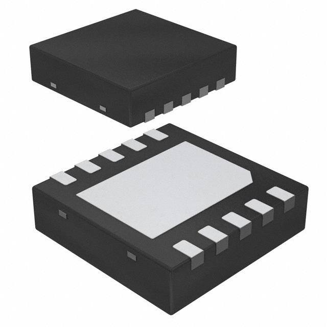
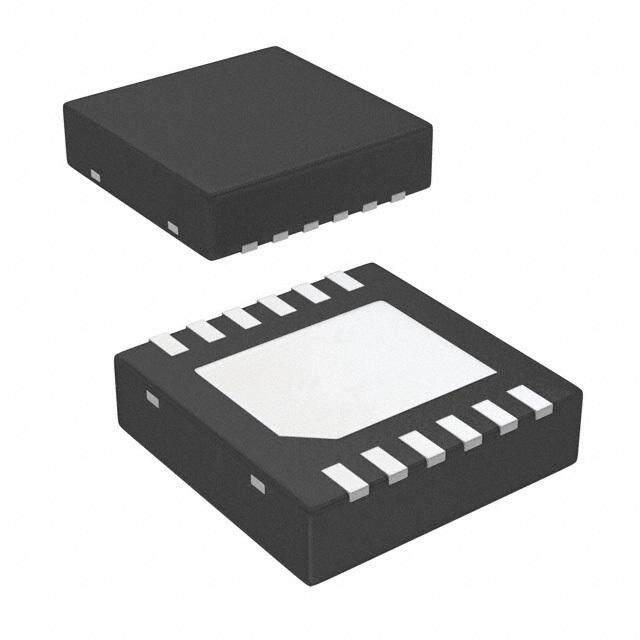
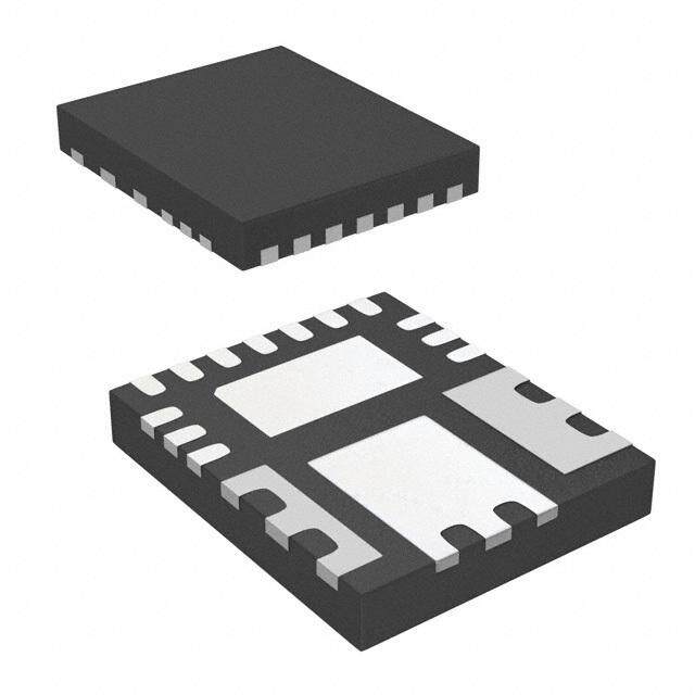
| 封装/外壳 | 10-WFDFN 裸露焊盘 |
| 封装/箱体 | WSON-10 |
| 工作温度 | -40°C ~ 85°C |
| 工作温度范围 | - 40 C to + 85 C |
| 工厂包装数量 | 250 |
| 开关频率 | 1.65 MHz |
| 拓扑结构 | Boost |
| 最大输入电压 | 5.5 V |
| 最小工作温度 | - 40 C |
| 标准包装 | 1 |
| 电压-输入 | 0.3 V ~ 5.5 V |
| 电压-输出 | 5V |
| 电流-输出 | 600mA |
| 类型 | 升压(升压) |
| 系列 | TPS61202 |
| 输出数 | 1 |
| 输出电压 | 5 V |
| 输出电流 | 600 mA |
| 输出端数量 | 1 Output |
| 输出类型 | 固定 |
| 配用 | /product-detail/zh/TPS61202EVM-179/296-31238-ND/1908023/product-detail/zh/SMP-TPS61202-MVK/SMP-TPS61202-MVK-ND/3431130 |
| 频率-开关 | 1.25MHz ~ 1.65MHz |


- 商务部:美国ITC正式对集成电路等产品启动337调查
- 曝三星4nm工艺存在良率问题 高通将骁龙8 Gen1或转产台积电
- 太阳诱电将投资9.5亿元在常州建新厂生产MLCC 预计2023年完工
- 英特尔发布欧洲新工厂建设计划 深化IDM 2.0 战略
- 台积电先进制程称霸业界 有大客户加持明年业绩稳了
- 达到5530亿美元!SIA预计今年全球半导体销售额将创下新高
- 英特尔拟将自动驾驶子公司Mobileye上市 估值或超500亿美元
- 三星加码芯片和SET,合并消费电子和移动部门,撤换高东真等 CEO
- 三星电子宣布重大人事变动 还合并消费电子和移动部门
- 海关总署:前11个月进口集成电路产品价值2.52万亿元 增长14.8%


PDF Datasheet 数据手册内容提取
Product Sample & Technical Tools & Support & Folder Buy Documents Software Community TPS61200,TPS61201,TPS61202 SLVS577E–MARCH2007–REVISEDDECEMBER2014 TPS6120x Low Input Voltage Synchronous Boost Converter With 1.3-A Switches 1 Features 3 Description • Morethan90%Efficiencyat The TPS6120x devices provide a power supply 1 solution for products powered by either a single-cell, – 300mAOutputCurrentat3.3V two-cell, or three-cell alkaline, NiCd or NiMH, or one- (VIN ≥2.4V) cell Li-Ion or Li-polymer battery. It is also used in fuel – 600mAOutputCurrentat5V(VIN ≥ 3V) cellorsolarcellpowereddeviceswherethecapability • AutomaticTransitionbetweenBoostModeand of handling low input voltages is essential. Possible output currents depend on the input to output voltage DownConversionMode ratio. The devices provide output currents of up to • DeviceQuiescentCurrentLessthan55 μA 600 mA at a 5-V output, while using a single-cell Li- • StartupintoFullLoadat0.5VInputVoltage Ion or Li-Polymer battery and discharges it down to • OperatingInputVoltageRangefrom 2.6 V. The boost converter is based on a fixed frequency, pulse-width-modulation (PWM) controller 0.3Vto5.5V using synchronous rectification to obtain maximum • ProgrammableUndervoltageLockoutThreshold efficiency. At low load currents, the converter enters • OutputShortCircuitProtectionUnderall the Power Save mode to maintain a high efficiency OperatingConditions over a wide load current range. The Power Save mode can be disabled, forcing the converter to • FixedandAdjustableOutputVoltageOptionsfrom operate at a fixed switching frequency. The average 1.8Vto5.5V input current is limited to a maximum value of 1500 • PowerSaveModeforImprovedEfficiencyatLow mA. The output voltage is programmed by an OutputPower external resistor divider, or is fixed internally on the • ForcedFixedFrequencyOperationPossible chip. The converter can be disabled to minimize batterydrain.Duringshutdown,theloadiscompletely • LoadDisconnectDuringShutdown disconnected from the battery. The device is • OvertemperatureProtection packaged in a 10-pin VSON package measuring 3 • Small3mmx3mmVSON-10Package mmx3mm. 2 Applications DeviceInformation(1) • AllSingle-Cell,Two-CellandThree-CellAlkaline, PARTNUMBER PACKAGE BODYSIZE(NOM) NiCdorNiMHorSingle-CellLiBatteryPowered TPS6120x VSON(10) 3.00mm×3.00mm Products (1) For all available packages, see the orderable addendum at theendofthedatasheet. • FuelCellAndSolarCellPoweredProducts • PortableAudioPlayers • PDAs • CellularPhones • PersonalMedicalProducts • WhiteLEDDriver 4 Typical Application L 1 2.2mH C VIN L VIN 1 VOUT 0.3 V to 5.5 V EN C 10mF PS VAUX C3 R1 2 V1.O8 UVT to 5.5 V UVLO 0.1mF 10mF FB GND PGND R2 TPS61200 1 An IMPORTANT NOTICE at the end of this data sheet addresses availability, warranty, changes, use in safety-critical applications, intellectualpropertymattersandotherimportantdisclaimers.PRODUCTIONDATA.
TPS61200,TPS61201,TPS61202 SLVS577E–MARCH2007–REVISEDDECEMBER2014 www.ti.com Table of Contents 1 Features.................................................................. 1 10.3 FeatureDescription...............................................12 2 Applications........................................................... 1 10.4 DeviceFunctionalModes......................................13 3 Description............................................................. 1 11 ApplicationandImplementation........................ 14 4 TypicalApplication................................................ 1 11.1 ApplicationInformation..........................................14 11.2 TypicalApplication ...............................................14 5 RevisionHistory..................................................... 2 11.3 SystemExamples.................................................19 6 DeviceOptions....................................................... 4 12 PowerSupplyRecommendations..................... 20 7 PinConfigurationandFunctions......................... 4 13 Layout................................................................... 21 8 Specifications......................................................... 5 13.1 LayoutGuidelines.................................................21 8.1 AbsoluteMaximumRatings......................................5 13.2 LayoutExample....................................................21 8.2 ESDRatings..............................................................5 13.3 ThermalConsiderations........................................21 8.3 RecommendedOperatingConditions.......................5 14 DeviceandDocumentationSupport................. 22 8.4 ThermalInformation..................................................5 14.1 RelatedLinks........................................................22 8.5 ElectricalCharacteristics...........................................6 14.2 Trademarks...........................................................22 8.6 TypicalCharacteristics..............................................7 14.3 ElectrostaticDischargeCaution............................22 9 ParameterMeasurementInformation................10 14.4 Glossary................................................................22 10 DetailedDescription........................................... 11 15 Mechanical,Packaging,andOrderable 10.1 Overview...............................................................11 Information........................................................... 22 10.2 FunctionalBlockDiagram.....................................11 5 Revision History NOTE:Pagenumbersforpreviousrevisionsmaydifferfrompagenumbersinthecurrentversion. ChangesfromRevisionD(March2013)toRevisionE Page • AddedESDRatingstable,FeatureDescriptionsection,DeviceFunctionalModes,ApplicationandImplementation section,PowerSupplyRecommendationssection,Layoutsection,DeviceandDocumentationSupportsection,and Mechanical,Packaging,andOrderableInformationsection.................................................................................................. 1 ChangesfromRevisionC(September2012)toRevisionD Page • ChangedthePSpindescriptionFrom:Enable/disablePowerSavemode(High=enabled,Low=disabled)To: Enable/disablePowerSavemode(High=disabled,Low=enabled)................................................................................... 4 ChangesfromRevisionB(FEBRUARY2008)toRevisionC Page • ChangedFeatureFrom:Small3mmx3mmQFN-10PackageTo:Small3mmx3mmSON-10Package......................1 • ChangedApplicationFrom:WhiteLED'sTo:WhiteLEDDriver............................................................................................ 1 • ChangedtheAvailableDeviceOptionsPackagetypeFrom:10-PINQFNTo:10-PinSON................................................. 4 • ChangedV toV intheRecommendedOperatingConditionstable................................................................................. 5 SS IN • ChangedFrom:DISSIPATIONRATINGSTABLETo:ThermalInformationtable ................................................................ 5 • ChangedtheParametersandTestConditionsintheElectricalCharacteristicstable .......................................................... 6 • UpdatedFigure1throughFigure11...................................................................................................................................... 7 • AddedC3totheListofComponents................................................................................................................................... 14 • AddedtexttotheInputCapacitorsection"AnR-Cfiltermaybeplaced..."......................................................................... 16 • AddedFigure26,Figure27,andFigure28......................................................................................................................... 19 • AddedFigure29................................................................................................................................................................... 21 2 SubmitDocumentationFeedback Copyright©2007–2014,TexasInstrumentsIncorporated ProductFolderLinks:TPS61200 TPS61201 TPS61202
TPS61200,TPS61201,TPS61202 www.ti.com SLVS577E–MARCH2007–REVISEDDECEMBER2014 ChangesfromRevisionA(JUNE2007)toRevisionB Page • AddedDSCpackageandtapeandreelnotetotheAvailableDeviceOptions..................................................................... 4 ChangesfromOriginal(MARCH2007)toRevisionA Page • ChangedFeaturesbulletFrom:600mAOutputCurrentat3.3V(VIN≥1.2V)To:300mAOutputCurrentat3.3V (VIN≥2.4V)........................................................................................................................................................................... 1 • ChangedFigure6labelFrom:PowerSaveDisabledTo:PowerSaveEnabled .................................................................. 7 • ChangedFigure7labelFrom:PowerSaveEnabledTo:PowerSaveDisabled .................................................................. 8 Copyright©2007–2014,TexasInstrumentsIncorporated SubmitDocumentationFeedback 3 ProductFolderLinks:TPS61200 TPS61201 TPS61202
TPS61200,TPS61201,TPS61202 SLVS577E–MARCH2007–REVISEDDECEMBER2014 www.ti.com 6 Device Options T OUTPUTVOLTAGE(1) PARTNUMBER(2) A Adjustable TPS61200DRC 3.3V TPS61201DRC –40°Cto85°C 5V TPS61202DRC 5V TPS61202DSC (1) Contactthefactorytocheckavailabilityofotherfixedoutputvoltageversions. (2) TheDRCandtheDSCpackageareavailabletapedandreeled.AddRsuffixtodevicetype(e.g.,TPS61200DRCRorTPS61202DSCR) toorderquantitiesof3000devicesperreel.Itisalsoavailableinminireels.AddaTsuffixtothedevicetype(i.e.TPS61200DRCTor TPS61202DSCT)toorderquantitiesof250devicesperreel. 7 Pin Configuration and Functions DSCandDRCPackage 10Pins TopView VAUX 1 10 FB VOUT 2 Exposed 9 GND L 3 Thermal 8 PS Pad PGND 4 7 UVLO VIN 5 6 EN PinFunctions PIN I/O DESCRIPTION NAME NO. EN 6 I Enableinput(High=enabled,Low=disabled).Donotleavefloating. Exposed — — Mustbesolderedtoachieveappropriatepowerdissipationandmechanicalreliability.Shouldbe thermalpad connectedtoPGND. FB 10 I Voltagefeedbackofadjustableversions,mustbeconnectedtoV atfixedoutputvoltageversions OUT GND 9 — Control/logicground PGND 4 — Powerground PS 8 I Enable/disablePowerSavemode(High=disabled,Low=enabled).Donotleavefloating. L 3 I ConnectionforInductor UVLO 7 I Undervoltagelockoutcomparatorinput.MustbeconnectedtoVAUXifnotused VAUX 1 I/O Supplyvoltageforcontrolstage VIN 5 I Boostconverterinputvoltage VOUT 2 O Boostconverteroutput 4 SubmitDocumentationFeedback Copyright©2007–2014,TexasInstrumentsIncorporated ProductFolderLinks:TPS61200 TPS61201 TPS61202
TPS61200,TPS61201,TPS61202 www.ti.com SLVS577E–MARCH2007–REVISEDDECEMBER2014 8 Specifications 8.1 Absolute Maximum Ratings overoperatingfree-airtemperaturerange(unlessotherwisenoted)(1) MIN MAX UNIT V InputvoltagerangeonVIN,L,VAUX,VOUT,PS,EN,FB,UVLO –0.3 7 V IN T Operatingjunctiontemperature –40 150 °C J T Storagetemperature –65 150 °C stg (1) StressesbeyondthoselistedunderAbsoluteMaximumRatingsmaycausepermanentdamagetothedevice.Thesearestressratings only,andfunctionaloperationofthedeviceattheseoranyotherconditionsbeyondthoseindicatedunderRecommendedOperating Conditionsisnotimplied.Exposuretoabsolute-maximum-ratedconditionsforextendedperiodsmayaffectdevicereliability. 8.2 ESD Ratings VALUE UNIT Human-bodymodel(HBM),perANSI/ESDA/JEDECJS-001(1) ±4000 Charged-devicemodel(CDM),perJEDECspecificationJESD22- ±1500 V(ESD) Electrostaticdischarge C101(2) V MachineModel(MM)(3) ±200 (1) JEDECdocumentJEP155statesthat500-VHBMallowssafemanufacturingwithastandardESDcontrolprocess.Manufacturingwith lessthan500-VHBMispossiblewiththenecessaryprecautions. (2) JEDECdocumentJEP157statesthat250-VCDMallowssafemanufacturingwithastandardESDcontrolprocess.Manufacturingwith lessthan250-VCDMispossiblewiththenecessaryprecautions. (3) ESDtestingisperformedaccordingtotherespectiveJESD22JEDECstandard. 8.3 Recommended Operating Conditions MIN NOM MAX UNIT V InputvoltageatVIN 0.3 5.5 V IN T Operatingfreeairtemperaturerange –40 85 °C A T Operatingjunctiontemperaturerange –40 125 °C J 8.4 Thermal Information TPS6120x THERMALMETRIC(1) DRC DSC UNIT 10PINS 10PINS R Junction-to-ambientthermalresistance 41.2 40.4 θJA R Junction-to-case(top)thermalresistance 62.8 37.8 θJC(top) R Junction-to-boardthermalresistance 16.6 15.4 θJB °C/W ψ Junction-to-topcharacterizationparameter 1.2 0.3 JT ψ Junction-to-boardcharacterizationparameter 16.8 15.6 JB R Junction-to-case(bottom)thermalresistance 4.1 2.8 θJC(bot) (1) Formoreinformationabouttraditionalandnewthermalmetrics,seetheICPackageThermalMetricsapplicationreport,SPRA953. Copyright©2007–2014,TexasInstrumentsIncorporated SubmitDocumentationFeedback 5 ProductFolderLinks:TPS61200 TPS61201 TPS61202
TPS61200,TPS61201,TPS61202 SLVS577E–MARCH2007–REVISEDDECEMBER2014 www.ti.com 8.5 Electrical Characteristics overrecommendedjunctiontemperaturerangeandoverrecommendedinputvoltagerange(typicalatanambient temperaturerangeof25°C)(unlessotherwisenoted) PARAMETER TESTCONDITIONS MIN TYP MAX UNIT DC-DCSTAGE VIN Inputvoltagerange 0.3 5.5 V VIN Minimuminputvoltageatstartup 0.5 V VOUT TPS61200outputvoltagerange 1.8 5.5 V VFB TPS61200feedbackvoltage 495 500 505 mV VOUT TPS61201outputvoltage VIN<VOUT,PS=High 3.27 3.3 3.33 V VOUT TPS61202outputvoltage VIN<VOUT,PS=High 4.95 5.0 5.05 V f Oscillatorfrequency 1250 1650 kHz ILIM averageinductorcurrentlimit VOUT=3.3V 1200 1350 1500 mA RDS(on) Rectifyingswitchonresistance VOUT=3.3V 180 mΩ RDS(on) Mainswitchonresistance VOUT=3.3V 150 mΩ Lineregulation VIN<VOUT,PS=High 0.1% 0.5% Loadregulation VIN<VOUT,PS=High 0.1% 0.5% VIN IO=0mA,VEN=VIN=1.2V, 1 2 μA IQ Quiescentcurrent VOUT VOUT=3.3V,VAUX=3.3V 50 70 μA PS=Low VAUX 4 6 μA VIN 0.5 1.5 μA ISD Shutdowncurrent VEN=0V,VIN=1.2V VAUX 1 2 μA ILKG Inputleakagecurrent(L) VEN=0V,VIN=1.2V,VL=1.2V 0.01 1 μA CONTROLSTAGE VAUX AuxiliaryOutputVoltage 2.4 5.5 V VIL Lowlevelinputthresholdvoltage(EN) VIN<0.8V 0.1×VIN V VIH Highlevelinputthresholdvoltage(EN) VIN<0.8V 0.9×VIN V VIL Lowlevelinputthresholdvoltage(EN) 0.8V≤VIN≤1.5V 0.2×VIN V VIH Highlevelinputthresholdvoltage(EN) 0.8V≤VIN≤1.5V 0.8×VIN V VIL Lowlevelinputthresholdvoltage(EN) VIN>1.5V 0.4 V VIH Highlevelinputthresholdvoltage(EN) VIN>1.5V 1.2 V VIL Lowlevelinputthresholdvoltage(PS) 0.4 V VIH Highlevelinputthresholdvoltage(PS) 1.2 V ILKG Inputleakagecurrent(EN,PS) EN,PS=GNDorVIN 0.01 0.1 μA VUVLO Undervoltagelockoutthreshold FallingUVLOvoltage 235 250 265 mV VUVLO Undervoltagelockoutthreshold RisingUVLOvoltage 330 350 370 mV ILKG Inputleakagecurrent(UVLO) VUVLO=0.5V 0.3 μA VOVP Overvoltageprotectionthreshold 5.5 7 V Thermalshutdowntemperature Risingtemperature 140 °C Thermalshutdowntemperature 20 °C hysteresis 6 SubmitDocumentationFeedback Copyright©2007–2014,TexasInstrumentsIncorporated ProductFolderLinks:TPS61200 TPS61201 TPS61202
TPS61200,TPS61201,TPS61202 www.ti.com SLVS577E–MARCH2007–REVISEDDECEMBER2014 8.6 Typical Characteristics Table1.TableofGraphs FIGURE Maximumoutputcurrent vsInputvoltage Figure1 vsOutputcurrent(TPS61200),PowerSaveEnabled Figure2 vsOutputcurrent(TPS61200),PowerSaveDisabled Figure3 vsOutputcurrent(TPS61201),PowerSaveEnabled Figure4 vsOutputcurrent(TPS61201),PowerSaveDisabled Figure5 vsOutputcurrent(TPS61202),PowerSaveEnabled Figure6 Efficiency vsOutputcurrent(TPS61202),PowerSaveDisabled Figure7 vsInputvoltage(TPS61201),PowerSaveEnabled Figure8 vsInputvoltage(TPS61201),PowerSaveDisabled Figure9 vsInputvoltage(TPS61202),PowerSaveEnabled Figure10 vsInputvoltage(TPS61202),PowerSaveDisabled Figure11 vsOutputcurrent(TPS61201) Figure12 Outputvoltage vsOutputcurrent(TPS61202) Figure13 1600 100 TPS61201 TPS61200 1400 VO= 3.3 V 90 VO= 1.8 V, Power Save Enabled 80 A nt - m 1200 VTOPS=6 11.280 V0 70 VI= 1.8 V Curre 1000 y - % 60 ut 800 nc 50 p e m Out 600 TPS61202 Effici 40 VI= 0.9 V mu VO= 5 V 30 xi 400 a M 20 200 10 0 0 0.2 0.6 1 1.4 1.82.2 2.6 3 3.43.8 4.24.6 5 5.4 0.10 1 10 100 1000 VI- Input Voltage - V IO- Output Current - mA Figure1.MaximumOutputCurrentvsInputVoltage Figure2.EfficiencyvsOutputCurrent 100 100 TPS61200 TPS61201 90 VO= 1.8 V, VI= 1.8 V 90 VO= 3.3 V, VI= 2.4 V Power Save Disabled Power Save Enabled 80 80 70 70 y - % 60 y - % 60 VI= 1.8 V nc 50 nc 50 e e Effici 40 VI= 0.9 V Effici 40 VI= 0.9 V 30 30 20 20 10 10 0 0 0.10 1 10 100 1000 0.10 1 10 100 1000 IO- Output Current - mA IO- Output Current - mA Figure3.EfficiencyvsOutputCurrent Figure4.EfficiencyvsOutputCurrent Copyright©2007–2014,TexasInstrumentsIncorporated SubmitDocumentationFeedback 7 ProductFolderLinks:TPS61200 TPS61201 TPS61202
TPS61200,TPS61201,TPS61202 SLVS577E–MARCH2007–REVISEDDECEMBER2014 www.ti.com 100 100 TPS61201 VI= 3.6 V 90 VPOow=e 3r .S3 aVv,e Disabled 90 VI= 2.4 V 80 80 70 VI= 2.4 V 70 VI= 1.8 V y - % 60 VI= 1.8 V y - % 60 nc 50 nc 50 e e Effici 40 VI= 0.9 V Effici 40 VI= 0.9 V 30 30 20 20 TPS61202 VO= 5 V, 10 10 Power Save Enabled 0 0 0.10 1 10 100 1000 0.10 1 10 100 1000 IO- Output Current - mA IO- Output Current - mA Figure5.EfficiencyvsOutputCurrent Figure6.EfficiencyvsOutputCurrent 100 100 TPS61202 VI= 3.6 V IO= 500 mA IO= 1000 mA 90 VO= 5 V, 90 Power Save Disabled IO= 100 mA 80 80 VI= 2.4 V 70 70 Efficiency - % 456000 VI= 0.9 VVI= 1.8 V Efficiency - % 456000 IO= 10 mA 30 30 20 20 TPS61201 VO= 3.3 V, 10 10 Power Save Enabled 0 0 0.10 1 10 100 1k 10k 0 0.5 1 1.5 2 2.5 3 3.5 4 4.5 5 5.5 IO- Output Current - mA VI- Input Voltage - V Figure7.EfficiencyvsOutputCurrent Figure8.EfficiencyvsInputVoltage 100 100 IO= 500 mA IO= 1000 mA IO= 500 mA 90 90 IO= 100 mA 80 80 70 70 IO= 1000 mA Efficiency - % 456000 IO= 100I Om=A 10 mA Efficiency - % 456000 IO= 10 mA 30 30 20 TPS61201 20 TPS61202 VO= 3.3 V, VO= 5 V, 10 Power Save Disabled 10 Power Save Enabled 0 0 0 0.5 1 1.5 2 2.5 3 3.5 4 4.5 5 5.5 0 0.5 1 1.5 2 2.5 3 3.5 4 4.5 5 5.5 VI- Input Voltage - V VI- Input Voltage - V Figure9.EfficiencyvsInputVoltage Figure10.EfficiencyvsInputVoltage 8 SubmitDocumentationFeedback Copyright©2007–2014,TexasInstrumentsIncorporated ProductFolderLinks:TPS61200 TPS61201 TPS61202
TPS61200,TPS61201,TPS61202 www.ti.com SLVS577E–MARCH2007–REVISEDDECEMBER2014 100 3.33 90 VI= 2.4 V 80 IO= 500 mA 70 IO= 100 mA IO= 1000 mA V ncy - % 5600 Voltage - Efficie 40 IO= 10 mA utput 3.30 O 30 - O V TPS61202 20 VO= 5 V, TPS61201 Power Save Disabled 10 VO= 3.3 V, Power Save Disabled 0 0 0.5 1 1.5 2 2.5 3 3.5 4 4.5 5 5.5 3.27 VI- Input Voltage - V 1 10 100 1000 IO- Output Current - mA Figure11.EfficiencyvsInputVoltage Figure12.OutputVoltagevsOutputCurrent 5.05 TPS61202 VO= 5 V, Power Save Disabled VI= 2.4 V V e - g a olt ut V 5 p ut O - O V 4.95 1 10 100 1000 IO- Output Current - mA Figure13.OutputVoltagevsOutputCurrent Copyright©2007–2014,TexasInstrumentsIncorporated SubmitDocumentationFeedback 9 ProductFolderLinks:TPS61200 TPS61201 TPS61202
TPS61200,TPS61201,TPS61202 SLVS577E–MARCH2007–REVISEDDECEMBER2014 www.ti.com 9 Parameter Measurement Information L1 VIN VIN L VOUT C1 VOUT EN VAUX R1 C2 PS C3 UVLO FB R2 GND PGND TPS61200 Figure14. ParameterMeasurementSchematic 10 SubmitDocumentationFeedback Copyright©2007–2014,TexasInstrumentsIncorporated ProductFolderLinks:TPS61200 TPS61201 TPS61202
TPS61200,TPS61201,TPS61202 www.ti.com SLVS577E–MARCH2007–REVISEDDECEMBER2014 10 Detailed Description 10.1 Overview The TPS6120x is a low input voltage synchronous boost converter family. The devices support 0.3-V to 5.5-V input voltage range, so can provide power supply solutions for products powered by either a single-cell, two-cell, orthree-cellalkaline,NiCdorNiMH,orone-cellLi-IonorLi-polymerbattery.Itisalsousedinfuelcellorsolarcell powered devices where the capability of handling low input voltages is essential. The devices provide output currents of up to 600 mA at a 5-V output, while using a single-cell Li-Ion or Li-Polymer battery and discharges it down to 2.6 V. The boost converter is based on a fixed frequency, pulse-width-modulation (PWM) controller using synchronous rectification to obtain maximum efficiency. At low load currents, the converter enters the Power Save mode to maintain a high efficiency over a wide load current range. The Power Save mode can be disabled, forcing the converter to operate at a fixed switching frequency. The average input current is limited to a maximum value of 1500 mA. The output voltage is programmed by an external resistor divider, or is fixed internally on the chip. The converter can be disabled to minimize battery drain. During shutdown, the load is completelydisconnectedfromthebattery. 10.2 Functional Block Diagram L VOUT VAUX VCC Current Control VOUT Sensor PGND VIN Gate VCC Control Modulator FB V FB PS Oscillator EN Device Control UVLO Thermal PGND Shutdown GND PGND Copyright©2007–2014,TexasInstrumentsIncorporated SubmitDocumentationFeedback 11 ProductFolderLinks:TPS61200 TPS61201 TPS61202
TPS61200,TPS61201,TPS61202 SLVS577E–MARCH2007–REVISEDDECEMBER2014 www.ti.com 10.3 Feature Description 10.3.1 ControllerCircuit The controlling circuit of the device is based on an average current mode topology. The average inductor current is regulated by a fast current regulator loop which is controlled by a voltage control loop. The controller also uses input and output voltage feedforward. Changes of input and output voltage are monitored and immediately change the duty cycle in the modulator to achieve a fast response to those errors. The voltage error amplifier gets its feedback input from the FB pin. For adjustable output voltage devices, a resistive voltage divider must be connected to that pin. For fixed output voltage devices, FB must be connected to the output voltage to directly sense the voltage. Fixed output voltage versions use a trimmed internal resistive divider. The feedback voltage is comparedwiththeinternalreferencevoltagetogenerateastableandaccurateoutputvoltage. Thecontrollercircuitalsosensestheaverageinputcurrentaswellasthepeakinputcurrent.Thus,themaximum input power is controlled as well as the maximum peak current, to achieve a safe and stable operation under all possibleconditions.Toprotectthedevicefromoverheating,aninternaltemperaturesensorisimplemented. 10.3.1.1 SynchronousOperation The device uses three internal N-channel MOSFETs to maintain synchronous power conversion at all possible operating conditions. This enables the device to keep high efficiency over a wide input voltage and output power range. To avoid ground shift problems due to the high currents in the switches, two separate ground pins, GND and PGND, are used. The reference for all control functions is the GND pin. The power switches are connected to PGND. Both grounds must be connected on the PCB at only one point, ideally close to the GND pin. Due to the 3-switchtopology,theloadisalwaysdisconnectedfromtheinputduringshutdownoftheconverter. 10.3.1.2 DownRegulation A boost converter only regulates output voltages which are higher than the input voltage. This device operates differently. For example, it is able to regulate 3 V at the output with two fresh alkaline cells at the input having a total cell voltage of 3.2 V. Another example is powering white LEDs with a forward voltage of 3.6 V from a fully charged Li-Ion cell with an output voltage of 4.2 V. To control these applications properly, a Down Conversion modeisimplemented. If the input voltage reaches or exceeds the output voltage, the converter automatically changes to a Down Conversion mode. In this mode, the control circuit changes the behavior of the two rectifying switches. While continuing switching, it sets the voltage drop across the rectifying switches as high as needed to regulate the output voltage. This means the power losses in the converter increase. This must be taken into account for thermalconsideration. 10.3.1.3 DeviceEnable The device is put into operation when EN is set high. It is put into Shutdown mode when EN is set to low. In Shutdown mode, the regulator stops switching, all internal control circuitry including the UVLO comparator is switched off, and the load is disconnected from the input. Current does not flow from input to output or from outputtoinput.Thisalsomeansthattheoutputvoltagecandropbelowtheinputvoltageduringshutdown. 10.3.1.4 SoftstartandShort-CircuitProtection During start-up of the converter, the duty cycle and the peak current are limited in order to avoid high peak currentsdrawnfromthebattery.Afterbeingenabled,thedevicestartsoperating.Atfirst,itkeepsthemainoutput VOUTdisconnected,andchargesthecapacitoratVAUX.OncethecapacitoratVAUXischargedtoabout2.5V, the device switches to normal operation. This means VOUT is turned on and the capacitor at VOUT is charged, while the load connected to the device is supplied. To ramp up the output voltage in a controlled way, the average current limit is set to 400 mA and rises proportional to the increase of the output voltage. At an output voltage of about 1.2 V the current limit is at its nominal value. If the output voltage does not increase, the current limit does not increase. There is no timer implemented. Thus the output voltage overshoot at startup, as well as theinrushcurrent,iskeptataminimum.Thedevicerampsuptheoutputvoltageinacontrolledmannerevenifa large capacitor is connected at the output. When the output voltage does not increase above 1.2 V, the device assumes a short-circuit at the output, and keeps the current limit low to protect itself and the application. When thereisashortattheoutputduringoperation,thecurrentlimitisdecreasedaccordingly. 12 SubmitDocumentationFeedback Copyright©2007–2014,TexasInstrumentsIncorporated ProductFolderLinks:TPS61200 TPS61201 TPS61202
TPS61200,TPS61201,TPS61202 www.ti.com SLVS577E–MARCH2007–REVISEDDECEMBER2014 Feature Description (continued) ThedevicecanalsostartintoaPrebiasontheoutputs. 10.3.1.5 CurrentLimit The device current limit limits the average current in the inductor. In a boost connector, this is the input current. If an excessive load requires an input current greater than the average current limit, the device limits the input currentbyreducingtheoutputpowerdelivered.Inthiscase,theoutputvoltagedecreases. 10.3.1.6 UndervoltageLockout An undervoltage lockout function prevents the main output at VOUT from being supplied if the voltage at the UVLO pin drops below 0.25 V. When using a resistive divider at the voltage to be monitored, for example the supplyvoltage,anythresholdforthemonitoredvoltagecanbeprogrammed.Ifinundervoltagelockoutmode,the device still maintains its supply voltage at VAUX, and it is not turned off until EN is programmed low. This undervoltagelockoutfunctionisimplementedinordertopreventthemalfunctioningoftheconverter. 10.3.1.7 ThermalShutdown The device has a built-in temperature sensor which monitors the internal IC temperature. If the temperature exceeds the programmed threshold (see electrical characteristics table), the device stops operating. As soon as the IC temperature has decreased below the programmed threshold, it starts operating again. There is a built-in hysteresistoavoidunstableoperationatICtemperaturesatthethermalshutdownthreshold. 10.4 Device Functional Modes 10.4.1 PowerSaveMode The Power Save (PS) pin can be used to select different operation modes. To enable Power Save mode the PS pin must be set low. Power Save mode is used to improve efficiency at light load. If Power Save mode is enabled, the converter stops operating if the average inductor current decreases below about 300 mA and the output voltage is at or above its nominal value. If the output voltage decreases below its nominal value, the device ramps up the output voltage again by starting operation using a programmed average inductor current higher than required by the current load condition. Operation can last for one or several pulses. The converter stopsoperatingoncetheconditionsforstoppingoperationaremetagain. The Power Save mode can be disabled by programming a high at the PS pin. In Down Conversion mode, Power Save mode is always enabled and the device cannot be forced into fixed frequency operation at light loads. The PSinputsupportsstandardlogicthresholds. 10.4.2 DownConversionMode If the input voltage reaches or exceeds the output voltage, the converter automatically changes to a Down Conversion mode. In this mode, the control circuit changes the behavior of the two rectifying switches. While continuing switching, it sets the voltage drop across the rectifying switches as high as needed to regulate the output voltage. This means the power losses in the converter increase. This must be taken into account for thermalconsideration. Copyright©2007–2014,TexasInstrumentsIncorporated SubmitDocumentationFeedback 13 ProductFolderLinks:TPS61200 TPS61201 TPS61202
TPS61200,TPS61201,TPS61202 SLVS577E–MARCH2007–REVISEDDECEMBER2014 www.ti.com 11 Application and Implementation NOTE Information in the following applications sections is not part of the TI component specification, and TI does not warrant its accuracy or completeness. TI’s customers are responsible for determining suitability of components for their purposes. Customers should validateandtesttheirdesignimplementationtoconfirmsystemfunctionality. 11.1 Application Information The TPS6120x DC-DC converters are intended for systems powered by a single up to triple cell Alkaline, NiCd, NiMH battery with a typical terminal voltage between 0.7 V and 5.5 V. They can also be used in systems powered by one-cell Li-Ion or Li-Polymer with a typical voltage between 2.5 V and 4.2 V. Additionally, any other voltage source like solar cells or fuel cells with a typical output voltage between 0.3 V and 5.5 V can power systemswheretheTPS6120xisused. 11.2 Typical Application L1 VIN VIN L VOUT C1 VOUT R3 EN VAUX R1 C2 PS C3 UVLO FB R4 R2 GND PGND TPS61200 Figure15. TypicalApplicationCircuitforAdjustableOutputVoltageOption 11.2.1 DesignRequirements In this example, TPS61200 is used to design a 3.3-V power supply with 100-mA output current capability. The TPS61200canbepoweredbyeitherasingle-cell,two-cell,orthree-cellalkaline,NiCdorNiMH,orone-cellLi-Ion or Li-Polymer battery. In this example, the input voltage range is from 0.8 V to 1.65 V for single-cell alkaline input. 11.2.2 DetailedDesignProcedure Table2.ListofComponents COMPONENTREFERENCE PARTNUMBER MANUFACTURER VALUE C1 any 10μF,X7RCeramic C2 any 2x10μF,X7RCeramic C3 any 1µF,X7R,Ceramic L1 LPS3015-222ML Coilcraft 2.2μH 11.2.2.1 ProgrammingtheOutputVoltage Within the TPS6120X family, there are fixed and adjustable output voltage versions available. To properly configure the fixed output voltage devices, the FB pin is used to sense the output voltage. This means that it must be connected directly to VOUT. For the adjustable output voltage version, an external resistor divider is used to adjust the output voltage. The resistor divider must be connected between VOUT, FB and GND. When the output voltage is regulated properly, the typical value of the voltage at the FB pin is 500 mV. The maximum recommendedvaluefortheoutputvoltageis5.5V.Thecurrentthroughtheresistivedividershouldbeabout100 times greater than the current into the FB pin. The typical current into the FB pin is 0.01 μA, and the voltage 14 SubmitDocumentationFeedback Copyright©2007–2014,TexasInstrumentsIncorporated ProductFolderLinks:TPS61200 TPS61201 TPS61202
TPS61200,TPS61201,TPS61202 www.ti.com SLVS577E–MARCH2007–REVISEDDECEMBER2014 across the resistor between FB and GND, R2, is typically 500 mV. Based on those two values, the recommendedvalueforR2shouldbelowerthan500kΩ,inordertosetthedividercurrentat1 μAorhigher.Itis recommended to keep the value for this resistor in the range of 200 kΩ. The value of the resistor connected between VOUT and FB, R1, depending on the needed output voltage (V ), can be calculated using OUT Equation1: æV ö OUT R1=R2x ç -1÷ V è FB ø (1) As an example, for an output voltage of 3.3 V, a 1-MΩ resistor should be chosen for R when a 180-kΩ is 1 selectedforR . 2 11.2.2.2 ProgrammingtheUVLOThresholdVoltage The UVLO input can be used to shut down the main output if the supply voltage is getting too low. The internal reference threshold is typically 250 mV. If the supply voltage should cause the shutdown when it is dropping below250mV,V canbeconnecteddirectlytotheUVLOpin.Iftheshutdownshouldhappenathighervoltages, IN a resistor divider can be used. R3 and R4 in Figure 15 show an example of how to monitor the input voltage of the circuit. The current through the resistive divider should be about 100 times greater than the current into the UVLO pin. The typical current into the UVLO pin is 0.01 μA, and the voltage across R4 is equal to the UVLO voltagethresholdthatisgeneratedon-chip,whichhasavalueof250mV.Therefore,therecommendedvaluefor R4 is in the range of 250 kΩ. From this, the value of resistor R3, depending on the desired shutdown voltage V canbecalculatedusingEquation2. INMIN, æV ö INMIN R3=R4x ç -1÷ çV ÷ è UVLO ø (2) 11.2.2.3 InductorSelection To make sure that the TPS6120X devices can operate, an inductor must be connected between the VIN and L pins.Toestimatetheminimuminductancevalue,Equation3canbeused. ms L =V x0.5 MIN IN A (3) In Equation 3, the minimum inductance, L , for boost mode operation is calculated. V is the maximum input MIN IN voltage. The recommended inductor value range is between 1.5 μH and 4.7 μH. The minimum inductor value should not be below 1.5 μH, even if Equation 3 yields something lower. Using 2.2 μH is recommended anyway forgettingbestperformanceoverthewholeinputandoutputvoltagerange. With the chosen inductance value, the peak current for the inductor in steady state operation can be calculated usingEquation4. VOUT x IOUT VIN x (VOUT -VIN) I = + LMAX 0.8 xV 2 xV xfxL IN OUT (4) This would be the critical value for the current rating for selecting the inductor. It also needs to be taken into account that load transients and error conditions may cause higher inductor currents. The following inductor seriesfromdifferentsuppliershavebeenusedwithTPS6120xconverters: Table3.ListofInductors VENDOR INDUCTORSERIES LPS3015 Coilcraft LPS4012 Murata LQH3NP TajoYuden NR3015 WurthElektronik WE-TPCTypS Copyright©2007–2014,TexasInstrumentsIncorporated SubmitDocumentationFeedback 15 ProductFolderLinks:TPS61200 TPS61201 TPS61202
TPS61200,TPS61201,TPS61202 SLVS577E–MARCH2007–REVISEDDECEMBER2014 www.ti.com 11.2.2.4 CapacitorSelection 11.2.2.4.1 InputCapacitor At least a 4.7-μF input capacitor is recommended to improve transient behavior of the regulator and EMI behavior of the total power supply circuit. An X5R or X7R ceramic capacitor placed as close as possible to the VINandPGNDpinsoftheICisrecommended. An R-C filter may be placed on the VIN pin to improve performance in applications with a noisy input source. A 100-Ωresistorand0.1-µFcapacitorarerecommendedinthiscase.Thisfilterisnotrequiredoperation. 11.2.2.4.2 OutputCapacitor For the output capacitor, it is recommended to use small X5R or X7R ceramic capacitors placed as close as possible to the VOUT and PGND pins of the IC. If, for any reason, the application requires the use of large capacitors which can not be placed close to the IC, using a smaller ceramic capacitor in parallel to the large one isrequired.ThissmallcapacitorshouldbeplacedascloseaspossibletotheVOUTandPGNDpinsoftheIC. Togetanestimateoftherecommendedminimumoutputcapacitance,Equation5 canbeused. mF C =5xLx OUT mH (5) A capacitor with a value in the range of the calculated minimum should be used. This is required to maintain control loop stability. There are no additional requirements regarding minimum ESR. There is also no upper limit for the output capacitance value. Larger capacitors cause lower output voltage ripple as well as lower output voltagedropsduringloadtransients. 11.2.2.4.3 CapacitoratVAUX BetweentheVAUXpinandGNDpin,acapacitormustbeconnected.Thiscapacitorisusedtomaintainandfilter the control supply voltage, which is chosen from the highest of VIN, VOUT, and L. It is charged during startup and before the main output VOUT is turned on. To ensure stable operation, using at least 0.1μF is recommended. At output voltages below 2.5 V, the capacitance should be in the range of 1 μF. Since this capacitor is also used as a snubber capacitor for the main switch, using a X5R or X7R ceramic capacitor with lowESRisimportant. 11.2.3 ApplicationCurves FIGURE OutputVoltageTPS61201,PowerSaveModeDisabled Figure16 OutputVoltageTPS61202,PowerSaveModeDisabled Figure17 OutputVoltageTPS61201,PowerSaveModeEnabled Figure18 OutputVoltageTPS61202,PowerSaveModeEnabled Figure19 TPS61201LoadTransientResponse Figure20 TPS61202LoadTransientResponse Figure21 TPS61201LineTransientResponse Figure22 TPS61202LineTransientResponse Figure23 TPS61201StartupafterEnable Figure24 TPS61202StartupafterEnable Figure25 16 SubmitDocumentationFeedback Copyright©2007–2014,TexasInstrumentsIncorporated ProductFolderLinks:TPS61200 TPS61201 TPS61202
TPS61200,TPS61201,TPS61202 www.ti.com SLVS577E–MARCH2007–REVISEDDECEMBER2014 TVPOS=6 31.230 V1, VI= 1.8 V, RL= 11W TVPOS=6 51 2V0,2 VI= 1.8 V, RL= 17W Output Voltage20 mV/div,AC Power Save Disabled Output Voltage50 mV/div,AC Power Save Disabled nductor Current100 mA/div,AC nductor Current200 mA/div,AC I I t - Time - 0.5ms/div t - Time - 1ms/div Figure16.OutputVoltage,PowerSaveModeDisabled Figure17.OutputVoltage,PowerSaveModeDisabled VI= 1.8 V, RL= 33 kW TPS61202 VI= 1.8 V, RL= 55 kW VO= 5 V, Output Voltage20 mV/div,AC Output Voltage20 mV/div,AC Power Save Enabled nt nt CurreA/div CurreA/div nductor 100 m TPS61201 nductor 200 m I VO= 3.3 V, I Power Save Enabled t - Time - 2 ms/div t - Time - 100ms/div Figure18.OutputVoltageinPowerSaveMode Figure19.OutputVoltageinPowerSaveMode TPS61201 VI= 1.8 V, IL= 300 mAto 400 mA TPS61202 VI= 1.8 V, IL= 150 mAto 250 mA Output Voltage50 mV/div,AC VO= 3.3 V Output Voltage100 mV/div,AC VO= 5 V Output Current50 mA/div,AC Output Current100 mA/div,AC t - Time - 1 ms/div t - Time - 1 ms/div Figure20.LoadTransientResponse Figure21.LoadTransientResponse Copyright©2007–2014,TexasInstrumentsIncorporated SubmitDocumentationFeedback 17 ProductFolderLinks:TPS61200 TPS61201 TPS61202
TPS61200,TPS61201,TPS61202 SLVS577E–MARCH2007–REVISEDDECEMBER2014 www.ti.com VI= 1.8 V to 2.4 V, RL= 11W VI= 3 V to 3.6 V, RL= 17W geAC geAC oltadiv, oltadiv, ut VmV/ ut VmV/ Inp500 Inp500 ageAC ageAC Voltdiv, Voltdiv, put mV/ put mV/ ut0 ut0 O5 O2 TPS61202 TPS61201 VO= 3.3 V VO= 5 V t - Time - 2 ms/div t - Time - 2 ms/div Figure22.LineTransientResponse Figure23.LineTransientResponse Enable 5 V/div, DC Enable 5 V/div, DC Voltage at VAUX 2 V/div, DC Voltage at VAUX 2 V/div, DC Output Voltage 2 V/div, DC Output Voltage 2 V/div, DC Voltage at L2 V/div, DC Voltage at L2 V/div, DC Inductor Current 500 mA/div, DC Inductor Current 500 mA/div, DC TVPOS=6 31.230 V1 VI= 1.8 V, RL= 11W TVPOS=6 31.230 V1 VI= 1.8 V, RL= 17W t - Time - 100ms/div t - Time - 100ms/div Figure24.Start-UpAfterEnable Figure25.Start-UpAfterEnable 18 SubmitDocumentationFeedback Copyright©2007–2014,TexasInstrumentsIncorporated ProductFolderLinks:TPS61200 TPS61201 TPS61202
TPS61200,TPS61201,TPS61202 www.ti.com SLVS577E–MARCH2007–REVISEDDECEMBER2014 11.3 System Examples Figure26. WLEDDriverCircuit(SeeSLVA364) L1 4.7µH V = 0.3 - 0.5V cell VIN L V OUT 0 VOUT 0 R1 EN 2 Charge ell VCELL C1 VAUX UVLO 61 FB CFF storage C S R2 C2 device r PS P VAUX VAUX a ol T S C3 GND PGND RefDes Value C1 >10mF R5 C2 >20mF VAUX C3 1mF C4 C4 1mF C5 10 nF R3 C 33 pF FF R8 L1 4.7mH R6 RefDes Value R4 VCELL OPA379 R1 750 kW TLV431 R2 200 kW R3 1 kW R4 1 MW R7 Power ground R5 100W R6 1 MW MPP circuit C5 Reference ground R7 100 kW R8 200 kW Figure27. SolarCellCircuit(SeeSLVA345) Copyright©2007–2014,TexasInstrumentsIncorporated SubmitDocumentationFeedback 19 ProductFolderLinks:TPS61200 TPS61201 TPS61202
TPS61200,TPS61201,TPS61202 SLVS577E–MARCH2007–REVISEDDECEMBER2014 www.ti.com System Examples (continued) L1 Inductor 2.2uH 3.3V 0.9V to 1.5V R1 Vout Vin 100 TPS61200 VVaouuxt 12 190 GFBND 4C73uF 1C04uF R4 Battery 1C01uF 0R2 C2 PGVNINDL 345 678 PEUSNVLO 1K 100nF TPS61200 R5 R3 1K 1K Q1 MOSFET-N GND Figure28. ReverseBatteryProtectionCircuit(SeeSLVA315) 12 Power Supply Recommendations The power supply of TPS6120x DC-DC converters can be a single up to triple cell Alkaline, NiCd, NiMH battery with a typical terminal voltage between 0.7 V and 5.5 V. The TPS6120x can also be powered by one-cell Li-Ion or Li-Polymer with a typical voltage between 2.5 V and 4.2 V. Additionally, any other voltage source like solar cellsorfuelcellswithatypicaloutputvoltagebetween0.3Vand5.5Vcanalsobethepowersupply. The input supply should be well regulated with the rating of TPS6120x. If the input supply is located more than a few inches from the device, additional bulk capacitance may be required in addition to the ceramic bypass capacitors.Anelectrolyticortantalumcapacitorwithavalueof47 µFisatypicalchoice. 20 SubmitDocumentationFeedback Copyright©2007–2014,TexasInstrumentsIncorporated ProductFolderLinks:TPS61200 TPS61201 TPS61202
TPS61200,TPS61201,TPS61202 www.ti.com SLVS577E–MARCH2007–REVISEDDECEMBER2014 13 Layout 13.1 Layout Guidelines As for all switching power supplies, the layout is an important step in the design, especially at high peak currents and high switching frequencies. If the layout is not carefully done, the regulator could show stability problems as well as EMI problems. Therefore, use wide and short traces for the main current path and for the power ground tracks. The input and output capacitor, as well as the inductor should be placed as close as possible to the IC. Use a common ground node for power ground and a different one for control ground to minimize the effects of groundnoise.ConnectthesegroundnodesatanyplaceclosetooneofthegroundpinsoftheIC. The feedback divider should be placed as close as possible to the control ground pin of the IC. To lay out the control ground, it is recommended to use short traces as well, separated from the power ground traces. This avoids ground shift problems, which can occur due to superimposition of power ground current and control groundcurrent.SeeFigure29fortherecommendedlayout. 13.2 Layout Example Figure29. EVMLayout 13.3 Thermal Considerations Implementation of integrated circuits in low-profile and fine-pitch surface-mount packages typically requires special attention to power dissipation. Many system-dependent issues such as thermal coupling, airflow, added heat sinks and convection surfaces, and the presence of other heat-generating components affect the power- dissipationlimitsofagivencomponent. Threebasicapproachesforenhancingthermalperformancearelistedbelow. • ImprovingthepowerdissipationcapabilityofthePCBdesign • ImprovingthethermalcouplingofthecomponenttothePCB • Introducingairflowinthesystem The maximum recommended junction temperature (T ) of the TPS6120x devices is 125°C. The thermal J resistance of the 10-pin SON 3 × 3 package (DRC) is R = 41.2 °C/W, when the exposed thermal pad is θJA soldered. Specified regulator operation is assured to a maximum ambient temperature, T , of 85°C. Therefore, A the maximum power dissipation is about 971 mW. More power can be dissipated if the maximum ambient temperatureoftheapplicationislower. T -T 125°C-85°C P = J(MAX) A = =971mW D(MAX) R 41.2°C/W qJA (6) Copyright©2007–2014,TexasInstrumentsIncorporated SubmitDocumentationFeedback 21 ProductFolderLinks:TPS61200 TPS61201 TPS61202
TPS61200,TPS61201,TPS61202 SLVS577E–MARCH2007–REVISEDDECEMBER2014 www.ti.com 14 Device and Documentation Support 14.1 Related Links The table below lists quick access links. Categories include technical documents, support and community resources,toolsandsoftware,andquickaccesstosampleorbuy. Table4.RelatedLinks TECHNICAL TOOLS& SUPPORT& PARTS PRODUCTFOLDER SAMPLE&BUY DOCUMENTS SOFTWARE COMMUNITY TPS61200 Clickhere Clickhere Clickhere Clickhere Clickhere TPS61201 Clickhere Clickhere Clickhere Clickhere Clickhere TPS61202 Clickhere Clickhere Clickhere Clickhere Clickhere 14.2 Trademarks Alltrademarksarethepropertyoftheirrespectiveowners. 14.3 Electrostatic Discharge Caution Thesedeviceshavelimitedbuilt-inESDprotection.Theleadsshouldbeshortedtogetherorthedeviceplacedinconductivefoam duringstorageorhandlingtopreventelectrostaticdamagetotheMOSgates. 14.4 Glossary SLYZ022—TIGlossary. Thisglossarylistsandexplainsterms,acronyms,anddefinitions. 15 Mechanical, Packaging, and Orderable Information The following pages include mechanical, packaging, and orderable information. This information is the most current data available for the designated devices. This data is subject to change without notice and revision of thisdocument.Forbrowser-basedversionsofthisdatasheet,refertotheleft-handnavigation. 22 SubmitDocumentationFeedback Copyright©2007–2014,TexasInstrumentsIncorporated ProductFolderLinks:TPS61200 TPS61201 TPS61202
PACKAGE OPTION ADDENDUM www.ti.com 24-Aug-2018 PACKAGING INFORMATION Orderable Device Status Package Type Package Pins Package Eco Plan Lead/Ball Finish MSL Peak Temp Op Temp (°C) Device Marking Samples (1) Drawing Qty (2) (6) (3) (4/5) TPS61200DRCR ACTIVE VSON DRC 10 3000 Green (RoHS CU NIPDAU Level-2-260C-1 YEAR -40 to 85 BRR & no Sb/Br) TPS61200DRCRG4 ACTIVE VSON DRC 10 3000 Green (RoHS CU NIPDAU Level-2-260C-1 YEAR -40 to 85 BRR & no Sb/Br) TPS61200DRCT ACTIVE VSON DRC 10 250 Green (RoHS CU NIPDAU Level-2-260C-1 YEAR -40 to 85 BRR & no Sb/Br) TPS61201DRCR ACTIVE VSON DRC 10 3000 Green (RoHS CU NIPDAU Level-2-260C-1 YEAR -40 to 85 BRS & no Sb/Br) TPS61201DRCT ACTIVE VSON DRC 10 250 Green (RoHS CU NIPDAU Level-2-260C-1 YEAR -40 to 85 BRS & no Sb/Br) TPS61202DRCR ACTIVE VSON DRC 10 3000 Green (RoHS CU NIPDAU Level-2-260C-1 YEAR -40 to 85 BRT & no Sb/Br) TPS61202DRCT ACTIVE VSON DRC 10 250 Green (RoHS CU NIPDAU Level-2-260C-1 YEAR -40 to 85 BRT & no Sb/Br) TPS61202DSCR ACTIVE WSON DSC 10 3000 Green (RoHS CU NIPDAU Level-2-260C-1 YEAR -40 to 85 CER & no Sb/Br) TPS61202DSCT ACTIVE WSON DSC 10 250 Green (RoHS CU NIPDAU Level-2-260C-1 YEAR -40 to 85 CER & no Sb/Br) TPS61202DSCTG4 ACTIVE WSON DSC 10 250 Green (RoHS CU NIPDAU Level-2-260C-1 YEAR -40 to 85 CER & no Sb/Br) (1) The marketing status values are defined as follows: ACTIVE: Product device recommended for new designs. LIFEBUY: TI has announced that the device will be discontinued, and a lifetime-buy period is in effect. NRND: Not recommended for new designs. Device is in production to support existing customers, but TI does not recommend using this part in a new design. PREVIEW: Device has been announced but is not in production. Samples may or may not be available. OBSOLETE: TI has discontinued the production of the device. (2) RoHS: TI defines "RoHS" to mean semiconductor products that are compliant with the current EU RoHS requirements for all 10 RoHS substances, including the requirement that RoHS substance do not exceed 0.1% by weight in homogeneous materials. Where designed to be soldered at high temperatures, "RoHS" products are suitable for use in specified lead-free processes. TI may reference these types of products as "Pb-Free". RoHS Exempt: TI defines "RoHS Exempt" to mean products that contain lead but are compliant with EU RoHS pursuant to a specific EU RoHS exemption. Green: TI defines "Green" to mean the content of Chlorine (Cl) and Bromine (Br) based flame retardants meet JS709B low halogen requirements of <=1000ppm threshold. Antimony trioxide based flame retardants must also meet the <=1000ppm threshold requirement. (3) MSL, Peak Temp. - The Moisture Sensitivity Level rating according to the JEDEC industry standard classifications, and peak solder temperature. Addendum-Page 1
PACKAGE OPTION ADDENDUM www.ti.com 24-Aug-2018 (4) There may be additional marking, which relates to the logo, the lot trace code information, or the environmental category on the device. (5) Multiple Device Markings will be inside parentheses. Only one Device Marking contained in parentheses and separated by a "~" will appear on a device. If a line is indented then it is a continuation of the previous line and the two combined represent the entire Device Marking for that device. (6) Lead/Ball Finish - Orderable Devices may have multiple material finish options. Finish options are separated by a vertical ruled line. Lead/Ball Finish values may wrap to two lines if the finish value exceeds the maximum column width. Important Information and Disclaimer:The information provided on this page represents TI's knowledge and belief as of the date that it is provided. TI bases its knowledge and belief on information provided by third parties, and makes no representation or warranty as to the accuracy of such information. Efforts are underway to better integrate information from third parties. TI has taken and continues to take reasonable steps to provide representative and accurate information but may not have conducted destructive testing or chemical analysis on incoming materials and chemicals. TI and TI suppliers consider certain information to be proprietary, and thus CAS numbers and other limited information may not be available for release. In no event shall TI's liability arising out of such information exceed the total purchase price of the TI part(s) at issue in this document sold by TI to Customer on an annual basis. Addendum-Page 2
PACKAGE MATERIALS INFORMATION www.ti.com 12-Jan-2018 TAPE AND REEL INFORMATION *Alldimensionsarenominal Device Package Package Pins SPQ Reel Reel A0 B0 K0 P1 W Pin1 Type Drawing Diameter Width (mm) (mm) (mm) (mm) (mm) Quadrant (mm) W1(mm) TPS61200DRCR VSON DRC 10 3000 330.0 12.4 3.3 3.3 1.1 8.0 12.0 Q2 TPS61200DRCR VSON DRC 10 3000 330.0 12.4 3.3 3.3 1.1 8.0 12.0 Q2 TPS61200DRCT VSON DRC 10 250 180.0 12.4 3.3 3.3 1.1 8.0 12.0 Q2 TPS61200DRCT VSON DRC 10 250 180.0 12.4 3.3 3.3 1.1 8.0 12.0 Q2 TPS61201DRCR VSON DRC 10 3000 330.0 12.4 3.3 3.3 1.1 8.0 12.0 Q2 TPS61201DRCR VSON DRC 10 3000 330.0 12.4 3.3 3.3 1.1 8.0 12.0 Q2 TPS61201DRCT VSON DRC 10 250 180.0 12.4 3.3 3.3 1.1 8.0 12.0 Q2 TPS61202DRCR VSON DRC 10 3000 330.0 12.4 3.3 3.3 1.1 8.0 12.0 Q2 TPS61202DRCR VSON DRC 10 3000 330.0 12.4 3.3 3.3 1.1 8.0 12.0 Q2 TPS61202DRCT VSON DRC 10 250 180.0 12.4 3.3 3.3 1.1 8.0 12.0 Q2 TPS61202DSCR WSON DSC 10 3000 330.0 12.4 3.3 3.3 1.1 8.0 12.0 Q2 TPS61202DSCT WSON DSC 10 250 180.0 12.4 3.3 3.3 1.1 8.0 12.0 Q2 PackMaterials-Page1
PACKAGE MATERIALS INFORMATION www.ti.com 12-Jan-2018 *Alldimensionsarenominal Device PackageType PackageDrawing Pins SPQ Length(mm) Width(mm) Height(mm) TPS61200DRCR VSON DRC 10 3000 367.0 367.0 35.0 TPS61200DRCR VSON DRC 10 3000 367.0 367.0 35.0 TPS61200DRCT VSON DRC 10 250 210.0 185.0 35.0 TPS61200DRCT VSON DRC 10 250 210.0 185.0 35.0 TPS61201DRCR VSON DRC 10 3000 367.0 367.0 35.0 TPS61201DRCR VSON DRC 10 3000 367.0 367.0 35.0 TPS61201DRCT VSON DRC 10 250 210.0 185.0 35.0 TPS61202DRCR VSON DRC 10 3000 367.0 367.0 35.0 TPS61202DRCR VSON DRC 10 3000 367.0 367.0 35.0 TPS61202DRCT VSON DRC 10 250 210.0 185.0 35.0 TPS61202DSCR WSON DSC 10 3000 367.0 367.0 35.0 TPS61202DSCT WSON DSC 10 250 210.0 185.0 35.0 PackMaterials-Page2
GENERIC PACKAGE VIEW DRC 10 VSON - 1 mm max height PLASTIC SMALL OUTLINE - NO LEAD Images above are just a representation of the package family, actual package may vary. Refer to the product data sheet for package details. 4204102-3/M
PACKAGE OUTLINE DRC0010J VSON - 1 mm max height SCALE 4.000 PLASTIC SMALL OUTLINE - NO LEAD 3.1 B A 2.9 PIN 1 INDEX AREA 3.1 2.9 1.0 C 0.8 SEATING PLANE 0.05 0.00 0.08 C 1.65 0.1 2X (0.5) (0.2) TYP EXPOSED 4X (0.25) THERMAL PAD 5 6 2X 11 SYMM 2 2.4 0.1 10 1 8X 0.5 0.30 10X 0.18 PIN 1 ID SYMM 0.1 C A B (OPTIONAL) 0.5 0.05 C 10X 0.3 4218878/B 07/2018 NOTES: 1. All linear dimensions are in millimeters. Any dimensions in parenthesis are for reference only. Dimensioning and tolerancing per ASME Y14.5M. 2. This drawing is subject to change without notice. 3. The package thermal pad must be soldered to the printed circuit board for optimal thermal and mechanical performance. www.ti.com
EXAMPLE BOARD LAYOUT DRC0010J VSON - 1 mm max height PLASTIC SMALL OUTLINE - NO LEAD (1.65) (0.5) 10X (0.6) 1 10 10X (0.24) 11 SYMM (2.4) (3.4) (0.95) 8X (0.5) 6 5 (R0.05) TYP ( 0.2) VIA TYP (0.25) (0.575) SYMM (2.8) LAND PATTERN EXAMPLE EXPOSED METAL SHOWN SCALE:20X 0.07 MIN 0.07 MAX EXPOSED METAL ALL AROUND ALL AROUND EXPOSED METAL SOLDER MASK METAL METAL UNDER SOLDER MASK OPENING SOLDER MASK OPENING NON SOLDER MASK SOLDER MASK DEFINED DEFINED (PREFERRED) SOLDER MASK DETAILS 4218878/B 07/2018 NOTES: (continued) 4. This package is designed to be soldered to a thermal pad on the board. For more information, see Texas Instruments literature number SLUA271 (www.ti.com/lit/slua271). 5. Vias are optional depending on application, refer to device data sheet. If any vias are implemented, refer to their locations shown on this view. It is recommended that vias under paste be filled, plugged or tented. www.ti.com
EXAMPLE STENCIL DESIGN DRC0010J VSON - 1 mm max height PLASTIC SMALL OUTLINE - NO LEAD 2X (1.5) (0.5) SYMM EXPOSED METAL 11 TYP 10X (0.6) 1 10 (1.53) 10X (0.24) 2X (1.06) SYMM (0.63) 8X (0.5) 6 5 (R0.05) TYP 4X (0.34) 4X (0.25) (2.8) SOLDER PASTE EXAMPLE BASED ON 0.125 mm THICK STENCIL EXPOSED PAD 11: 80% PRINTED SOLDER COVERAGE BY AREA SCALE:25X 4218878/B 07/2018 NOTES: (continued) 6. Laser cutting apertures with trapezoidal walls and rounded corners may offer better paste release. IPC-7525 may have alternate design recommendations. www.ti.com
None
PACKAGE OUTLINE DSC0010J WSON - 0.8 mm max height SCALE 4.000 PLASTIC SMALL OUTLINE - NO LEAD 3.1 B A 2.9 PIN 1 INDEX AREA 3.1 2.9 0.8 C 0.7 SEATING PLANE 0.05 0.00 0.08 C 1.65 0.1 2X (0.5) (0.2) TYP EXPOSED 4X (0.25) THERMAL PAD 5 6 2X 11 SYMM 2 2.4 0.1 10 1 8X 0.5 0.30 10X 0.18 PIN 1 ID SYMM 0.1 C A B (OPTIONAL) 0.5 0.05 C 10X 0.3 4221826/D 08/2018 NOTES: 1. All linear dimensions are in millimeters. Any dimensions in parenthesis are for reference only. Dimensioning and tolerancing per ASME Y14.5M. 2. This drawing is subject to change without notice. 3. The package thermal pad must be soldered to the printed circuit board for optimal thermal and mechanical performance. www.ti.com
EXAMPLE BOARD LAYOUT DSC0010J WSON - 0.8 mm max height PLASTIC SMALL OUTLINE - NO LEAD (1.65) (0.5) 10X (0.6) 1 10 10X (0.24) 11 SYMM (2.4) (3.4) (0.95) 8X (0.5) 6 5 (R0.05) TYP ( 0.2) VIA TYP (0.25) (0.575) SYMM (2.8) LAND PATTERN EXAMPLE EXPOSED METAL SHOWN SCALE:20X 0.07 MIN 0.07 MAX EXPOSED METAL ALL AROUND ALL AROUND EXPOSED METAL SOLDER MASK METAL METAL UNDER SOLDER MASK OPENING SOLDER MASK OPENING NON SOLDER MASK SOLDER MASK DEFINED DEFINED (PREFERRED) SOLDER MASK DETAILS 4221826/D 08/2018 NOTES: (continued) 4. This package is designed to be soldered to a thermal pad on the board. For more information, see Texas Instruments literature number SLUA271 (www.ti.com/lit/slua271). 5. Vias are optional depending on application, refer to device data sheet. If any vias are implemented, refer to their locations shown on this view. It is recommended that vias under paste be filled, plugged or tented. www.ti.com
EXAMPLE STENCIL DESIGN DSC0010J WSON - 0.8 mm max height PLASTIC SMALL OUTLINE - NO LEAD 2X (1.5) (0.5) SYMM EXPOSED METAL 11 TYP 10X (0.6) 1 10 (1.53) 10X (0.24) 2X (1.06) SYMM (0.63) 8X (0.5) 6 5 (R0.05) TYP 4X (0.34) 4X (0.25) (2.8) SOLDER PASTE EXAMPLE BASED ON 0.125 mm THICK STENCIL EXPOSED PAD 11: 80% PRINTED SOLDER COVERAGE BY AREA SCALE:25X 4221826/D 08/2018 NOTES: (continued) 6. Laser cutting apertures with trapezoidal walls and rounded corners may offer better paste release. IPC-7525 may have alternate design recommendations. www.ti.com
IMPORTANTNOTICE TexasInstrumentsIncorporated(TI)reservestherighttomakecorrections,enhancements,improvementsandotherchangestoits semiconductorproductsandservicesperJESD46,latestissue,andtodiscontinueanyproductorserviceperJESD48,latestissue.Buyers shouldobtainthelatestrelevantinformationbeforeplacingordersandshouldverifythatsuchinformationiscurrentandcomplete. TI’spublishedtermsofsaleforsemiconductorproducts(http://www.ti.com/sc/docs/stdterms.htm)applytothesaleofpackagedintegrated circuitproductsthatTIhasqualifiedandreleasedtomarket.AdditionaltermsmayapplytotheuseorsaleofothertypesofTIproductsand services. ReproductionofsignificantportionsofTIinformationinTIdatasheetsispermissibleonlyifreproductioniswithoutalterationandis accompaniedbyallassociatedwarranties,conditions,limitations,andnotices.TIisnotresponsibleorliableforsuchreproduced documentation.Informationofthirdpartiesmaybesubjecttoadditionalrestrictions.ResaleofTIproductsorserviceswithstatements differentfromorbeyondtheparametersstatedbyTIforthatproductorservicevoidsallexpressandanyimpliedwarrantiesforthe associatedTIproductorserviceandisanunfairanddeceptivebusinesspractice.TIisnotresponsibleorliableforanysuchstatements. BuyersandotherswhoaredevelopingsystemsthatincorporateTIproducts(collectively,“Designers”)understandandagreethatDesigners remainresponsibleforusingtheirindependentanalysis,evaluationandjudgmentindesigningtheirapplicationsandthatDesignershave fullandexclusiveresponsibilitytoassurethesafetyofDesigners'applicationsandcomplianceoftheirapplications(andofallTIproducts usedinorforDesigners’applications)withallapplicableregulations,lawsandotherapplicablerequirements.Designerrepresentsthat,with respecttotheirapplications,Designerhasallthenecessaryexpertisetocreateandimplementsafeguardsthat(1)anticipatedangerous consequencesoffailures,(2)monitorfailuresandtheirconsequences,and(3)lessenthelikelihoodoffailuresthatmightcauseharmand takeappropriateactions.DesigneragreesthatpriortousingordistributinganyapplicationsthatincludeTIproducts,Designerwill thoroughlytestsuchapplicationsandthefunctionalityofsuchTIproductsasusedinsuchapplications. TI’sprovisionoftechnical,applicationorotherdesignadvice,qualitycharacterization,reliabilitydataorotherservicesorinformation, including,butnotlimitedto,referencedesignsandmaterialsrelatingtoevaluationmodules,(collectively,“TIResources”)areintendedto assistdesignerswhoaredevelopingapplicationsthatincorporateTIproducts;bydownloading,accessingorusingTIResourcesinany way,Designer(individuallyor,ifDesignerisactingonbehalfofacompany,Designer’scompany)agreestouseanyparticularTIResource solelyforthispurposeandsubjecttothetermsofthisNotice. TI’sprovisionofTIResourcesdoesnotexpandorotherwisealterTI’sapplicablepublishedwarrantiesorwarrantydisclaimersforTI products,andnoadditionalobligationsorliabilitiesarisefromTIprovidingsuchTIResources.TIreservestherighttomakecorrections, enhancements,improvementsandotherchangestoitsTIResources.TIhasnotconductedanytestingotherthanthatspecifically describedinthepublisheddocumentationforaparticularTIResource. Designerisauthorizedtouse,copyandmodifyanyindividualTIResourceonlyinconnectionwiththedevelopmentofapplicationsthat includetheTIproduct(s)identifiedinsuchTIResource.NOOTHERLICENSE,EXPRESSORIMPLIED,BYESTOPPELOROTHERWISE TOANYOTHERTIINTELLECTUALPROPERTYRIGHT,ANDNOLICENSETOANYTECHNOLOGYORINTELLECTUALPROPERTY RIGHTOFTIORANYTHIRDPARTYISGRANTEDHEREIN,includingbutnotlimitedtoanypatentright,copyright,maskworkright,or otherintellectualpropertyrightrelatingtoanycombination,machine,orprocessinwhichTIproductsorservicesareused.Information regardingorreferencingthird-partyproductsorservicesdoesnotconstitutealicensetousesuchproductsorservices,orawarrantyor endorsementthereof.UseofTIResourcesmayrequirealicensefromathirdpartyunderthepatentsorotherintellectualpropertyofthe thirdparty,oralicensefromTIunderthepatentsorotherintellectualpropertyofTI. TIRESOURCESAREPROVIDED“ASIS”ANDWITHALLFAULTS.TIDISCLAIMSALLOTHERWARRANTIESOR REPRESENTATIONS,EXPRESSORIMPLIED,REGARDINGRESOURCESORUSETHEREOF,INCLUDINGBUTNOTLIMITEDTO ACCURACYORCOMPLETENESS,TITLE,ANYEPIDEMICFAILUREWARRANTYANDANYIMPLIEDWARRANTIESOF MERCHANTABILITY,FITNESSFORAPARTICULARPURPOSE,ANDNON-INFRINGEMENTOFANYTHIRDPARTYINTELLECTUAL PROPERTYRIGHTS.TISHALLNOTBELIABLEFORANDSHALLNOTDEFENDORINDEMNIFYDESIGNERAGAINSTANYCLAIM, INCLUDINGBUTNOTLIMITEDTOANYINFRINGEMENTCLAIMTHATRELATESTOORISBASEDONANYCOMBINATIONOF PRODUCTSEVENIFDESCRIBEDINTIRESOURCESOROTHERWISE.INNOEVENTSHALLTIBELIABLEFORANYACTUAL, DIRECT,SPECIAL,COLLATERAL,INDIRECT,PUNITIVE,INCIDENTAL,CONSEQUENTIALOREXEMPLARYDAMAGESIN CONNECTIONWITHORARISINGOUTOFTIRESOURCESORUSETHEREOF,ANDREGARDLESSOFWHETHERTIHASBEEN ADVISEDOFTHEPOSSIBILITYOFSUCHDAMAGES. UnlessTIhasexplicitlydesignatedanindividualproductasmeetingtherequirementsofaparticularindustrystandard(e.g.,ISO/TS16949 andISO26262),TIisnotresponsibleforanyfailuretomeetsuchindustrystandardrequirements. WhereTIspecificallypromotesproductsasfacilitatingfunctionalsafetyorascompliantwithindustryfunctionalsafetystandards,such productsareintendedtohelpenablecustomerstodesignandcreatetheirownapplicationsthatmeetapplicablefunctionalsafetystandards andrequirements.Usingproductsinanapplicationdoesnotbyitselfestablishanysafetyfeaturesintheapplication.Designersmust ensurecompliancewithsafety-relatedrequirementsandstandardsapplicabletotheirapplications.DesignermaynotuseanyTIproductsin life-criticalmedicalequipmentunlessauthorizedofficersofthepartieshaveexecutedaspecialcontractspecificallygoverningsuchuse. Life-criticalmedicalequipmentismedicalequipmentwherefailureofsuchequipmentwouldcauseseriousbodilyinjuryordeath(e.g.,life support,pacemakers,defibrillators,heartpumps,neurostimulators,andimplantables).Suchequipmentincludes,withoutlimitation,all medicaldevicesidentifiedbytheU.S.FoodandDrugAdministrationasClassIIIdevicesandequivalentclassificationsoutsidetheU.S. TImayexpresslydesignatecertainproductsascompletingaparticularqualification(e.g.,Q100,MilitaryGrade,orEnhancedProduct). Designersagreethatithasthenecessaryexpertisetoselecttheproductwiththeappropriatequalificationdesignationfortheirapplications andthatproperproductselectionisatDesigners’ownrisk.Designersaresolelyresponsibleforcompliancewithalllegalandregulatory requirementsinconnectionwithsuchselection. DesignerwillfullyindemnifyTIanditsrepresentativesagainstanydamages,costs,losses,and/orliabilitiesarisingoutofDesigner’snon- compliancewiththetermsandprovisionsofthisNotice. MailingAddress:TexasInstruments,PostOfficeBox655303,Dallas,Texas75265 Copyright©2018,TexasInstrumentsIncorporated