ICGOO在线商城 > 集成电路(IC) > PMIC - 稳压器 - DC DC 开关稳压器 > ICL7660ACBAZA

 Datasheet下载
- 型号: ICL7660ACBAZA
- 制造商: Intersil
- 库位|库存: xxxx|xxxx
- 要求:
| 数量阶梯 | 香港交货 | 国内含税 |
| +xxxx | $xxxx | ¥xxxx |
查看当月历史价格
查看今年历史价格
ICL7660ACBAZA产品简介:
ICGOO电子元器件商城为您提供ICL7660ACBAZA由Intersil设计生产,在icgoo商城现货销售,并且可以通过原厂、代理商等渠道进行代购。 ICL7660ACBAZA价格参考。IntersilICL7660ACBAZA封装/规格:PMIC - 稳压器 - DC DC 开关稳压器, 固定 充电泵 开关稳压器 IC 正或负 -Vin,2Vin 1 输出 45mA 8-SOIC(0.154",3.90mm 宽)。您可以下载ICL7660ACBAZA参考资料、Datasheet数据手册功能说明书,资料中有ICL7660ACBAZA 详细功能的应用电路图电压和使用方法及教程。
ICL7660ACBAZA 是 Renesas Electronics 提供的一款经典的电荷泵(Charge Pump)DC-DC开关稳压器。其主要功能是通过电荷泵技术将输入电压进行反相或倍增,生成负输出电压或加倍的正输出电压。以下是该型号的一些典型应用场景:

 1. 电池供电设备
   - ICL7660ACBAZA 常用于便携式电池供电设备中,例如手持电子设备、无线耳机、遥控器等。它可以将单节电池的正电压转换为负电压,为需要负电源的电路供电。
   - 在低功耗应用中,它能够高效地延长电池寿命。

 2. 运算放大器和模拟电路
   - 许多模拟电路(如运算放大器、比较器)需要双极性电源(正负电源)。ICL7660ACBAZA 可以从单一正电源生成负电压,为这些电路提供完整的电源解决方案。
   - 例如,在音频放大器中,它可用于生成负电源以支持双电源工作模式。

 3. 数据转换器
   - ADC(模数转换器)和DAC(数模转换器)有时需要负电源来实现更高的精度和性能。ICL7660ACBAZA 可以为这些器件提供稳定的负电压。

 4. LCD 和 OLED 显示屏驱动
   - 某些 LCD 或 OLED 显示屏需要负电压来驱动偏置电路。ICL7660ACBAZA 可以轻松满足这一需求,同时保持较低的功耗。

 5. 传感器和信号调理电路
   - 在工业自动化和物联网(IoT)领域,许多传感器和信号调理电路需要负电源。ICL7660ACBAZA 可以为这些电路提供稳定且高效的负电压。

 6. 通信设备
   - 在通信设备中,某些射频(RF)电路和滤波器可能需要负电压。ICL7660ACBAZA 的简单设计和高效率使其成为理想选择。

 7. 教育和实验平台
   - 由于其简单易用的设计,ICL7660ACBAZA 也广泛应用于教学和实验平台中,帮助学生和工程师理解电荷泵的工作原理及其实际应用。

 总结
ICL7660ACBAZA 的核心优势在于其简单的外围电路设计、低成本以及高效率的电荷泵转换能力。它适用于需要负电压或电压倍增的各种场景,尤其是在对功耗和成本敏感的应用中表现出色。
| 参数 | 数值 |
| 产品目录 | 集成电路 (IC)半导体 |
| 描述 | IC REG SWITCHD CAP DBL INV 8SOIC稳压器—开关式稳压器 W/ANNEAL CMOS VOLT CONVRTR 8 COM |
| 产品分类 | |
| 品牌 | Intersil |
| 产品手册 | |
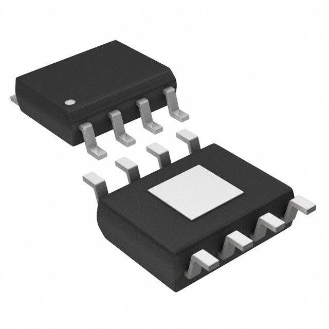
| 产品图片 |
|
| rohs | 符合RoHS无铅 / 符合限制有害物质指令(RoHS)规范要求 |
| 产品系列 | 电源管理 IC,稳压器—开关式稳压器,Intersil ICL7660ACBAZA- |
| 数据手册 | |
| 产品型号 | ICL7660ACBAZA |
| PCN组件/产地 | |
| PWM类型 | - |
| 产品种类 | 稳压器—开关式稳压器 |
| 供应商器件封装 | 8-SOIC |
| 包装 | 管件 |
| 同步整流器 | 无 |
| 商标 | Intersil |
| 安装类型 | 表面贴装 |
| 安装风格 | SMD/SMT |
| 宽度 | 4 mm (Max) |
| 封装 | Tube |
| 封装/外壳 | 8-SOIC(0.154",3.90mm 宽) |
| 封装/箱体 | SOIC-8 Narrow |
| 工作温度 | 0°C ~ 70°C |
| 工厂包装数量 | 98 |
| 开关频率 | 10 kHz |
| 最大工作温度 | + 70 C |
| 最大输入电压 | 12 V |
| 最小工作温度 | 0 C |
| 标准包装 | 98 |
| 电压-输入 | 1.5 V ~ 12 V |
| 电压-输出 | -1.5 V ~ -12 V |
| 电流-输出 | 45mA |
| 类型 | Charge Pumps |
| 系列 | ICL7660 |
| 输入电压 | 12 V |
| 输出数 | 1 |
| 输出电压 | - 1.5 V to - 12 V, 1.5 V to 18.6 V |
| 输出电流 | 45 mA |
| 输出类型 | 可调式 |
| 频率-开关 | 10kHz |


- 商务部:美国ITC正式对集成电路等产品启动337调查
- 曝三星4nm工艺存在良率问题 高通将骁龙8 Gen1或转产台积电
- 太阳诱电将投资9.5亿元在常州建新厂生产MLCC 预计2023年完工
- 英特尔发布欧洲新工厂建设计划 深化IDM 2.0 战略
- 台积电先进制程称霸业界 有大客户加持明年业绩稳了
- 达到5530亿美元!SIA预计今年全球半导体销售额将创下新高
- 英特尔拟将自动驾驶子公司Mobileye上市 估值或超500亿美元
- 三星加码芯片和SET,合并消费电子和移动部门,撤换高东真等 CEO
- 三星电子宣布重大人事变动 还合并消费电子和移动部门
- 海关总署:前11个月进口集成电路产品价值2.52万亿元 增长14.8%


PDF Datasheet 数据手册内容提取
DATASHEET ICL7660S, ICL7660A FN3179 Super Voltage Converters Rev 7.00 January 23, 2013 The ICL7660S and ICL7660A Super Voltage Converters are Features monolithic CMOS voltage conversion ICs that guarantee • Guaranteed Lower Max Supply Current for All significant performance advantages over other similar Temperature Ranges devices. They are direct replacements for the industry standard ICL7660 offering an extended operating supply • Wide Operating Voltage Range: 1.5V to 12V voltage range up to 12V, with lower supply current. A • 100% Tested at 3V Frequency Boost pin has been incorporated to enable the user to achieve lower output impedance despite using smaller • Boost Pin (Pin 1) for Higher Switching Frequency capacitors. All improvements are highlighted in the “Electrical • Guaranteed Minimum Power Efficiency of 96% Specifications” section on page3. Critical parameters are • Improved Minimum Open Circuit Voltage Conversion guaranteed over the entire commercial and industrial Efficiency of 99% temperature ranges. • Improved SCR Latchup Protection The ICL7660S and ICL7660A perform supply voltage conversions from positive to negative for an input range of • Simple Conversion of +5V Logic Supply to ±5V Supplies 1.5V to 12V, resulting in complementary output voltages of • Simple Voltage Multiplication VOUT = (-)nVIN -1.5V to -12V. Only two non-critical external capacitors are • Easy to Use; Requires Only Two External Non-Critical needed, for the charge pump and charge reservoir functions. Passive Components The ICL7660S and ICL7660A can be connected to function as a voltage doubler and will generate up to 22.8V with a • Improved Direct Replacement for Industry Standard 12V input. They can also be used as a voltage multipliers or ICL7660 and Other Second Source Devices voltage dividers. • Pb-Free Available (RoHS Compliant) Each chip contains a series DC power supply regulator, RC Applications oscillator, voltage level translator, and four output power MOS switches. The oscillator, when unloaded, oscillates at a • Simple Conversion of +5V to ±5V Supplies nominal frequency of 10kHz for an input supply voltage of • Voltage Multiplication VOUT = ±nVIN 5.0V. This frequency can be lowered by the addition of an external capacitor to the “OSC” terminal, or the oscillator • Negative Supplies for Data Acquisition Systems and may be over-driven by an external clock. Instrumentation • RS232 Power Supplies The “LV” terminal may be tied to GND to bypass the internal series regulator and improve low voltage (LV) operation. At • Supply Splitter, VOUT = ±VS medium to high voltages (3.5V to 12V), the LV pin is left floating to prevent device latchup. In some applications, an external Schottky diode from VOUT to CAP- is needed to guarantee latchup free operation (see Do’s and Dont’s section on page8). Pin Configurations ICL7660S ICL7660A (8 LD PDIP, SOIC) (8 LD PDIP, SOIC) TOP VIEW TOP VIEW BOOST 1 8 V+ NC 1 8 V+ CAP+ 2 7 OSC CAP+ 2 7 OSC GND 3 6 LV GND 3 6 LV CAP- 4 5 VOUT CAP- 4 5 VOUT FN3179 Rev 7.00 Page 1 of 13 January 23, 2013
ICL7660S, ICL7660A Ordering Information PART NUMBER TEMP. RANGE (NOTE 3) PART MARKING (°C) PACKAGE PKG. DWG. # ICL7660SCBA (Note 1) 7660 SCBA 0 to +70 8 Ld SOIC M8.15 ICL7660SCBAZ 7660 SCBAZ 0 to +70 8 Ld SOIC (Pb-free) M8.15 (Notes 1, 2) ICL7660SCPA 7660S CPA 0 to +70 8 Ld PDIP E8.3 ICL7660SCPAZ (Note 2) 7660S CPAZ 0 to +70 8 Ld PDIP (Pb-free; Note 4) E8.3 ICL7660SIBA (Note 1) 7660 SIBA -40 to +85 8 Ld SOIC M8.15 ICL7660SIBAZ 7660 SIBAZ -40 to +85 8 Ld SOIC (Pb-free) M8.15 (Notes 1, 2) ICL7660SIPA 7660 SIPA -40 to +85 8 Ld PDIP E8.3 ICL7660SIPAZ 7660S IPAZ -40 to +85 8 Ld PDIP (Pb-free; Note 4) E8.3 (Note 2) ICL7660ACBA (Note 1) 7660ACBA 0 to 70 8 Ld SOIC (N) M8.15 ICL7660ACBAZA 7660ACBAZ 0 to 70 8 Ld SOIC (N) (Pb-free) M8.15 (Notes1,2) ICL7660ACPA 7660ACPA 0 to 70 8 Ld PDIP E8.3 ICL7660ACPAZ (Note2) 7660ACPAZ 0 to 70 8 Ld PDIP (Pb-free; Note 4) E8.3 ICL7660AIBA (Note 1) 7660AIBA -40 to 85 8 Ld SOIC (N) M8.15 ICL7660AIBAZA 7660AIBAZ -40 to 85 8 Ld SOIC (N) (Pb-free) M8.15 (Notes1,2) NOTES: 1. Add “-T*” suffix for tape and reel. Please refer to TB347 for details on reel specifications. 2. These Intersil Pb-free plastic packaged products employ special Pb-free material sets, molding compounds/die attach materials, and 100% matte tin plate plus anneal (e3 termination finish, which is RoHS compliant and compatible with both SnPb and Pb-free soldering operations). Intersil Pb-free products are MSL classified at Pb-free peak reflow temperatures that meet or exceed the Pb-free requirements of IPC/JEDEC J STD-020. 3. For Moisture Sensitivity Level (MSL), please see device information page for ICL7660S, ICL7660A. For more information on MSL, please see Tech Brief TB363. 4. Pb-free PDIPs can be used for through-hole wave solder processing only. They are not intended for use in reflow solder processing applications. FN3179 Rev 7.00 Page 2 of 13 January 23, 2013
ICL7660S, ICL7660A Absolute Maximum Ratings Thermal Information Supply Voltage. . . . . . . . . . . . . . . . . . . . . . . . . . . . . . . . . . . . +13.0V Thermal Resistance (Typical, Notes 6, 7) JA (°C/W) JC (°C/W) LV and OSC Input Voltage (Note 5) 8 Ld PDIP*. . . . . . . . . . . . . . . . . . . . . . 110 59 V+ < 5.5V. . . . . . . . . . . . . . . . . . . . . . . . . . . . .-0.3V to V+ + 0.3V 8 Ld Plastic SOIC. . . . . . . . . . . . . . . . . 160 48 V+ > 5.5V. . . . . . . . . . . . . . . . . . . . . . . . . . .V+ -5.5V to V+ +0.3V Storage Temperature Range . . . . . . . . . . . . . . . . . .-65°C to +150°C Current into LV (Note 5) Pb-free reflow profile . . . . . . . . . . . . . . . . . . . . . . . . . .see link below V+ > 3.5V. . . . . . . . . . . . . . . . . . . . . . . . . . . . . . . . . . . . . . . .20µA http://www.intersil.com/pbfree/Pb-FreeReflow.asp Output Short Duration VSUPPLY 5.5V. . . . . . . . . . . . . . . . . . . . . . . . . . . . . .Continuous *Pb-free PDIPs can be used for through-hole wave solder processing only. They are not intended for use in reflow solder Operating Conditions processing applications. Temperature Range ICL7660SI, ICL7660AI. . . . . . . . . . . . . . . . . . . . . -40°C to +85°C ICL7660SC, ICL7660AC . . . . . . . . . . . . . . . . . . . . . 0°C to +70°C CAUTION: Do not operate at or near the maximum ratings listed for extended periods of time. Exposure to such conditions may adversely impact product reliability and result in failures not covered by warranty. NOTES: 5. Connecting any terminal to voltages greater than V+ or less than GND may cause destructive latchup. It is recommended that no inputs from sources operating from external supplies be applied prior to “power up” of ICL7660S and ICL7660A. 6. JA is measured with the component mounted on a low effective thermal conductivity test board in free air. See Tech Brief TB379 for details. 7. For JC, the “case temp” location is taken at the package top center. 8. Pb-free PDIPs can be used for through-hole wave solder processing only. They are not intended for use in reflow solder processing applications. Electrical Specifications ICL7660S and ICL7660A, V+ = 5V, TA = +25°C, OSC = Free running (see Figure 12, “ICL7660S Test Circuit” on page7 and Figure 13 “ICL7660A Test Circuit” on page7), unless otherwise specified. MIN MAX PARAMETER SYMBOL TEST CONDITIONS (Note 9) TYP (Note 9) UNITS Supply Current (Note 11) I+ RL = , +25°C - 80 160 µA 0°C < TA < +70°C - - 180 µA -40°C < TA < +85°C - - 180 µA -55°C < TA < +125°C - - 200 µA Supply Voltage Range - High V+H RL = 10k, LV Open, TMIN < TA < TMAX 3.0 - 12 V (Note 12) Supply Voltage Range - Low V+L RL = 10k, LV to GND, TMIN < TA < TMAX 1.5 - 3.5 V Output Source Resistance ROUT IOUT = 20mA - 60 100 IOUT = 20mA, 0°C < TA < +70°C - - 120 IOUT = 20mA, -25°C < TA < +85°C - - 120 IOUT = 20mA, -55°C < TA < +125°C - - 150 IOUT = 3mA, V+ = 2V, LV = GND, - - 250 0°C < TA < +70°C IOUT = 3mA, V+ = 2V, LV = GND, - - 300 -40°C < TA < +85°C IOUT = 3mA, V+ = 2V, LV = GND, - - 400 -55°C < TA < +125°C Oscillator Frequency (Note 10) fOSC COSC = 0, Pin 1 Open or GND 5 10 - kHz COSC = 0, Pin 1 = V+ - 35 - kHz Power Efficiency PEFF RL = 5k 96 98 - % TMIN < TA < TMAX RL = 5k 95 97 - - Voltage Conversion Efficiency VOUTEFF RL = 99 99.9 - % FN3179 Rev 7.00 Page 3 of 13 January 23, 2013
ICL7660S, ICL7660A Electrical Specifications ICL7660S and ICL7660A, V+ = 5V, TA = +25°C, OSC = Free running (see Figure 12, “ICL7660S Test Circuit” on page7 and Figure 13 “ICL7660A Test Circuit” on page7), unless otherwise specified. (Continued) MIN MAX PARAMETER SYMBOL TEST CONDITIONS (Note 9) TYP (Note 9) UNITS Oscillator Impedance ZOSC V+ = 2V - 1 - M V+ = 5V - 100 - k ICL7660A, V+ = 3V, TA = 25°C, OSC = Free running, Test Circuit Figure 13, unless otherwise specified Supply Current (Note 13) I+ V+ = 3V, RL = , +25°C - 26 100 A 0°C < TA < +70°C - - 125 A -40°C < TA < +85°C - - 125 A Output Source Resistance ROUT V+ = 3V, IOUT = 10mA - 97 150 0°C < TA < +70°C - - 200 -40°C < TA < +85°C - - 200 Oscillator Frequency (Note 13) fOSC V+ = 3V (same as 5V conditions) 5.0 8 - kHz 0°C < TA < +70°C 3.0 - - kHz -40°C < TA < +85°C 3.0 - - kHz NOTES: 9. Parameters with MIN and/or MAX limits are 100% tested at +25°C, unless otherwise specified. Temperature limits established by characterization and are not production tested. 10. In the test circuit, there is no external capacitor applied to pin 7. However, when the device is plugged into a test socket, there is usually a very small but finite stray capacitance present, on the order of 5pF. 11. The Intersil ICL7660S and ICL7660A can operate without an external diode over the full temperature and voltage range. This device will function in existing designs that incorporate an external diode with no degradation in overall circuit performance. 12. All significant improvements over the industry standard ICL7660 are highlighted. 13. Derate linearly above 50°C by 5.5mW/°C. FN3179 Rev 7.00 Page 4 of 13 January 23, 2013
ICL7660S, ICL7660A Functional Block Diagram V+ 8 Q1 OSCILLATOR VOLTAGE OSC AND DIVIDE-BY- LEVEL CAP+ 7 2 COUNTER TRANSLATOR 2 Q2 GND LV 3 6 CAP- Q4 4 INTERNAL SUPPLY REGULATOR VOUT 5 Q3 3 SUBSTRATE LOGIC 3 NETWORK 3 Typical Performance Curves See Figure 12, “ICL7660S Test Circuit” on page7) and Figure 13 “ICL7660A Test Circuit” on page7 12 250 Ω) TA = +125°C 10 CE ( 200 V) N AGE ( 8 SUPPLY VOLTAGE RANGE SISTA 150 TA = +25°C T (NO DIODE REQUIRED) E PPLY VOL 64 OURCE R 100 TA = -55°C U S S T U 50 2 P T U O 0 0 -55 -25 0 25 50 100 125 0 2 4 6 8 10 12 TEMPERATURE (°C) SUPPLY VOLTAGE (V) FIGURE 1. OPERATING VOLTAGE AS A FIGURE 2. OUTPUT SOURCE RESISTANCE AS A FUNCTION OF TEMPERATURE FUNCTION OF SUPPLY VOLTAGE 350 98 %) ANCE (Ω) 320500 CIENCY ( 9964 VTIOA+U ==T +5=2V 15m°CA ST IOUT = 3mA, FFI 92 ESI 200 IOUT = 20mA, V+ = 2V N E 90 OURCE R 150 V+ = 5V IVO+U T= =5 V20mA, NVERSIO 8886 OUTPUT S 10500 IOUT = 20mA, OWER CO 8842 0 V+ = 12V P 80 -50 -25 0 25 50 75 100 125 100 1k 10k 50k TEMPERATURE (°C) OSC FREQUENCY fOSC (Hz) FIGURE 3. OUTPUT SOURCE RESISTANCE AS A FIGURE 4. POWER CONVERSION EFFICIENCY AS A FUNCTION OF TEMPERATURE FUNCTION OF OSCILLATOR FREQUENCY FN3179 Rev 7.00 Page 5 of 13 January 23, 2013
ICL7660S, ICL7660A Typical Performance Curves See Figure 12, “ICL7660S Test Circuit” on page7) and Figure 13 “ICL7660A Test Circuit” on page7 (Continued) 10 20 (kHz)C 98 VTA+ == +52V5°C (kHz)C 18 OS OS Y f 7 Y f 16 C C N 6 N UE UE 14 EQ 5 EQ V+ = 10V R FR 4 R FR 12 CILLATO 32 CILLATO 10 V+ = 5V OS 1 OS 8 0 1 10 100 1k -55 -25 0 25 50 75 100 125 COSC (pF) TEMPERATURE (°C) FIGURE 5. FREQUENCY OF OSCILLATION AS A FUNCTION FIGURE 6. UNLOADED OSCILLATOR FREQUENCY AS A OF EXTERNAL OSCILLATOR CAPACITANCE FUNCTION OF TEMPERATURE 1 100 100 V+ = 5V Y (%) 90 90 0 TA = +25°C C EN 80 80 A) V) CI 70 70 m TAGE ( -1 N EFFI 60 60 RENT ( T VOL -2 ERSIO 5400 5400 Y CUR U V L TP -3 ON 30 30 PP U C U O R 20 V+ = 5V 20 S -4 E OW 10 TA = +25°C 10 P -5 0 0 0 10 20 30 40 50 60 0 10 20 30 40 LOAD CURRENT (mA) LOAD CURRENT (mA) FIGURE 7. OUTPUT VOLTAGE AS A FUNCTION FIGURE 8. SUPPLY CURRENT AND POWER CONVERSION OF OUTPUT CURRENT EFFICIENCY AS A FUNCTION OF LOAD CURRENT 2 100 V+ = 2V 90 TA = +25°C 12) 80 16 E UTPUT VOLTAGE (V) 10 OWER CONVERSIONEFFICIENCY (%) 7654300000 11186420 CURRENT (mA) (NOT O -1 P V+ = 2V Y 20 4 L TA = +25°C PP 10 2 U S -2 0 0 0 1 2 3 4 5 6 7 8 9 0 1.5 3.0 4.5 6.0 7.5 9.0 LOAD CURRENT (mA) LOAD CURRENT (mA) FIGURE 9. OUTPUT VOLTAGE AS A FUNCTION OF OUTPUT FIGURE 10. SUPPLY CURRENT AND POWER CONVERSION CURRENT EFFICIENCY AS A FUNCTION OF LOAD CURRENT FN3179 Rev 7.00 Page 6 of 13 January 23, 2013
ICL7660S, ICL7660A Typical Performance Curves See Figure 12, “ICL7660S Test Circuit” on page7) and Figure 13 “ICL7660A Test Circuit” on page7 (Continued) V+ = 5V TA = +25°C C1 = C2 = 1mF I = 10mA Ω) 400 E ( C1 = C2 = 10mF C N A 300 T SIS C1 = C2 = 100mF E R 200 T U P T U O 100 0 100 1k 10k 100k OSCILLATOR FREQUENCY (Hz) FIGURE 11. OUTPUT SOURCE RESISTANCE AS A FUNCTION OF OSCILLATOR FREQUENCY NOTE: 14. These curves include, in the supply current, that current fed directly into the load RL from the V+ (see Figure 12). Thus, approximately half the supply current goes directly to the positive side of the load, and the other half, through the ICL7660S and ICL7660A, goes to the negative side of the load. Ideally, VOUT 2VIN, IS 2IL, so VIN x IS VOUT x IL. V+ IS V+ IS V+ 1 8 (+5V) 1 8 (+5V) 2 7 2 7 IL C1 + ICL7660A IL ICL7660S 10µF 3 6 1C0µ1F+- 3 6 RL - 4 5 RL 4 5 -VOUT COSC (NOTE) - -VOUT C2 10µF + - C2 10µF + NOTE: For large values of COSC (>1000pF), the values of C1 and C2 should be increased to 100µF. FIGURE 12. ICL7660S TEST CIRCUIT NOTE: For large values of COSC (>1000pF) the values of C1 and C2 should be increased to 100F. FIGURE 13. ICL7660A TEST CIRCUIT FN3179 Rev 7.00 Page 7 of 13 January 23, 2013
ICL7660S, ICL7660A Detailed Description Theoretical Power Efficiency Considerations The ICL7660S and ICL7660A contain all the necessary circuitry to complete a negative voltage converter, with the In theory, a voltage converter can approach 100% efficiency exception of two external capacitors, which may be if certain conditions are met: inexpensive 10µF polarized electrolytic types. The mode of 1. The drive circuitry consumes minimal power. operation of the device may best be understood by considering Figure 14, which shows an idealized negative 2. The output switches have extremely low ON resistance voltage converter. Capacitor C1 is charged to a voltage, V+, and virtually no offset. for the half cycle, when switches S1 and S3 are closed. 3. The impedance of the pump and reservoir capacitors are (Note: Switches S2 and S4 are open during this half cycle). negligible at the pump frequency. During the second half cycle of operation, switches S2 and The ICL7660S and ICL7660A approach these conditions for S4 are closed, with S1 and S3 open, thereby shifting negative voltage conversion if large values of C1 and C2 are capacitor C1 to C2 such that the voltage on C2 is exactly V+, used. ENERGY IS LOST ONLY IN THE TRANSFER OF assuming ideal switches and no load on C2. The ICL7660S CHARGE BETWEEN CAPACITORS IF A CHANGE IN and ICL7660A approach this ideal situation more closely VOLTAGE OCCURS. The energy lost is defined as shown in than existing non-mechanical circuits. Equation1: 8 S1 2 S2 E = 1---C V 2–V 2 (EQ. 1) VIN 2 1 1 2 C1 where V1 and V2 are the voltages on C1 during the pump 3 3 and transfer cycles. If the impedances of C1 and C2 are relatively high at the pump frequency (see Figure 14) C2 compared to the value of RL, there will be a substantial S3 S4 5 difference in the voltages, V1 and V2. Therefore it is not only desirable to make C2 as large as possible to eliminate output 4 VOUT = -VIN voltage ripple, but also to employ a correspondingly large value for C1 in order to achieve maximum efficiency of operation. 7 Do’s and Don’ts FIGURE 14. IDEALIZED NEGATIVE VOLTAGE CONVERTER 1. Do not exceed maximum supply voltages. In the ICL7660S and ICL7660A, the four switches of 2. Do not connect LV terminal to GND for supply voltage Figure14 are MOS power switches; S1 is a P-Channel greater than 3.5V. device; and S2, S3 and S4 are N-Channel devices. The main 3. Do not short circuit the output to V+ supply for supply difficulty with this approach is that in integrating the switches, voltages above 5.5V for extended periods; however, the substrates of S3 and S4 must always remain reverse transient conditions including start-up are okay. biased with respect to their sources, but not so much as to 4. When using polarized capacitors, the + terminal of C1 must degrade their “ON” resistances. In addition, at circuit start- be connected to pin 2 of the ICL7660S and ICL7660A, and up, and under output short circuit conditions (VOUT = V+), the +terminal of C2 must be connected to GND. the output voltage must be sensed and the substrate bias 5. If the voltage supply driving the ICL7660S and ICL7660A adjusted accordingly. Failure to accomplish this would result has a large source impedance (25 to 30), then a in high power losses and probable device latch-up. 2.2µF capacitor from pin 8 to ground may be required to limit the rate of rise of input voltage to less than 2V/µs. This problem is eliminated in the ICL7660S and ICL7660A by a logic network that senses the output voltage (VOUT) 6. If the input voltage is higher than 5V and it has a rise rate together with the level translators, and switches the more than 2V/µs, an external Schottky diode from VOUT to CAP- is needed to prevent latchup (triggered by substrates of S3 and S4 to the correct level to maintain forward biasing Q4’s body diode) by keeping the output necessary reverse bias. (pin 5) from going more positive than CAP- (pin 4). The voltage regulator portion of the ICL7660S and 7. User should ensure that the output (pin 5) does not go ICL7660A is an integral part of the anti-latchup circuitry; more positive than GND (pin 3). Device latch-up will however, its inherent voltage drop can degrade operation at occur under these conditions. To provide additional low voltages. Therefore, to improve low voltage operation, protection, a 1N914 or similar diode placed in parallel the “LV” pin should be connected to GND, thus disabling the with C2 will prevent the device from latching up under regulator. For supply voltages greater than 3.5V, the LV these conditions, when the load on VOUT creates a path terminal must be left open to ensure latchup-proof operation to pull up VOUT before the IC is active (anode pin 5, cathode pin 3). and to prevent device damage. FN3179 Rev 7.00 Page 8 of 13 January 23, 2013
ICL7660S, ICL7660A Typical Applications charge the capacitors every cycle. Equation 4 shows a typical application where fOSC = 10kHz and C = C1 = C2 = 10µF: Simple Negative Voltage Converter The majority of applications will undoubtedly utilize the 1 R 2x23+---------------------------------------------------+4xESR +ESR ICL7660S and ICL7660A for generation of negative supply 0 3 –6 C1 C2 510 1010 (EQ. 4) voltages. Figure15 shows typical connections to provide a R 46+20+5ESR negative supply where a positive supply of +1.5V to +12V is 0 C available. Keep in mind that pin 6 (LV) is tied to the supply Since the ESRs of the capacitors are reflected in the output negative (GND) for supply voltage below 3.5V. impedance multiplied by a factor of 5, a high value could potentially swamp out a low 1/fPUMP x C1 term, rendering an V+ increase in switching frequency or filter capacitance ineffective. Typical electrolytic capacitors may have ESRs as 1 8 high as 10. 10µF 2 7 ICL7660S + ICL7660A Output Ripple 3 6 - RO VOUT ESR also affects the ripple voltage seen at the output. The 4 5 peak-to-peak output ripple voltage is given by Equation 5: - V+ 10µF+- VOUT = -V+ + VRIPPLE2----------f----------1---------------C------+2ESRC2IOUT (EQ. 5) PUMP 2 15A. 15B. A low ESR capacitor will result in a higher performance output. FIGURE 15. SIMPLE NEGATIVE CONVERTER AND ITS OUTPUT EQUIVALENT Paralleling Devices The output characteristics of the circuit in Figure 15 can be Any number of ICL7660S and ICL7660A voltage converters approximated by an ideal voltage source in series with a may be paralleled to reduce output resistance. The reservoir resistance as shown in Figure 15B. The voltage source has capacitor, C2, serves all devices, while each device requires a value of -(V+). The output impedance (RO) is a function of its own pump capacitor, C1. The resultant output resistance the ON resistance of the internal MOS switches (shown in is approximated in Equation 6: Figure 14), the switching frequency, the value of C1 and C2, R and the ESR (equivalent series resistance) of C1 and C2. A ROUT = n-------n--O-u---Um----T-b----e-o--r-f- - -oI-C--f-- L-d--7--e-6--v-6--i-0c---Se----s---- (EQ. 6) good first order approximation for RO is shown in Equation2: Cascading Devices R02RSW1+RSW3+ESRC1+2RSW2+RSW4+ESRC1 The ICL7660S and ICL7660A may be cascaded as shown to produce larger negative multiplication of the initial supply 1 --------------------------------+ESR voltage. However, due to the finite efficiency of each device, f C C2 (EQ. 2) PUMP 1 the practical limit is 10 devices for light loads. The output f voltage is defined as shown in Equation 7: f = --O-----S----C--- R =MOSFET Switch Resistance PUMP 2 SWX V = –nV (EQ. 7) OUT IN Combining the four RSWX terms as RSW, we see in where n is an integer representing the number of devices Equation 3 that: cascaded. The resulting output resistance would be R 2xR +---------------1-----------------+4xESR +ESR (EQ. 3) approximately the weighted sum of the individual ICL7660S 0 SW f C C1 C2 PUMP 1 and ICL7660A ROUT values. RSW, the total switch resistance, is a function of supply Changing the ICL7660S and ICL7660A Oscillator voltage and temperature (see the output source resistance Frequency graphs, Figures 2, 3, and 11), typically 23 at +25°C and 5V. It may be desirable in some applications, due to noise or other Careful selection of C1 and C2 will reduce the remaining considerations, to alter the oscillator frequency. This can be terms, minimizing the output impedance. High value achieved simply by one of several methods. capacitors will reduce the 1/(fPUMP x C1) component, and low By connecting the Boost Pin (Pin 1) to V+, the oscillator ESR capacitors will lower the ESR term. Increasing the charge and discharge current is increased and, hence, the oscillator frequency will reduce the 1/(fPUMP x C1) term, but oscillator frequency is increased by approximately 3.5 times. may have the side effect of a net increase in output The result is a decrease in the output impedance and ripple. impedance when C1 > 10µF and is not long enough to fully FN3179 Rev 7.00 Page 9 of 13 January 23, 2013
ICL7660S, ICL7660A This is of major importance for surface mount applications Positive Voltage Doubling where capacitor size and cost are critical. Smaller The ICL7660S and ICL7660A may be employed to achieve capacitors, such as 0.1µF, can be used in conjunction with positive voltage doubling using the circuit shown in Figure the Boost Pin to achieve similar output currents compared to 18. In this application, the pump inverter switches of the the device free running with C1 = C2 = 10µF or 100µF. (see ICL7660S and ICL7660A are used to charge C1 to a voltage Figure 11). level of V+ -VF, where V+ is the supply voltage and VF is the Increasing the oscillator frequency can also be achieved by forward voltage on C1, plus the supply voltage (V+) is overdriving the oscillator from an external clock, as shown in applied through diode D2 to capacitor C2. The voltage thus Figure 16. In order to prevent device latchup, a 1k resistor created on C2 becomes (2V+) - (2VF) or twice the supply must be used in series with the clock output. In a situation voltage minus the combined forward voltage drops of diodes where the designer has generated the external clock D1 and D2. frequency using TTL logic, the addition of a 10k pull-up The source impedance of the output (VOUT) will depend on resistor to V+ supply is required. Note that the pump the output current, but for V+ = 5V and an output current of frequency with external clocking, as with internal clocking, 10mA, it will be approximately 60. will be one-half of the clock frequency. Output transitions occur on the positive going edge of the clock. V+ V+ V+ 1 8 2 7 D1 ICL7660S 1 8 1kΩ 3 ICL7660A 6 D2 VOUT = + 2 ICL7660S 7 CGMATOES 4 5 + (2V+) - (2VF) 10µF- 3 ICL7660A 6 + -C2 C1 4 5 - VOUT - 10µF + NOTE: D1 AND D2 CAN BE ANY SUITABLE DIODE. FIGURE 16. EXTERNAL CLOCKING FIGURE 18. POSITIVE VOLTAGE DOUBLER It is also possible to increase the conversion efficiency of the Combined Negative Voltage Conversion and ICL7660S and ICL7660A at low load levels by lowering the Positive Supply Doubling oscillator frequency. This reduces the switching losses, and Figure 19 combines the functions shown in Figure 15 and is shown in Figure 17. However, lowering the oscillator Figure 18 to provide negative voltage conversion and frequency will cause an undesirable increase in the positive voltage doubling simultaneously. This approach impedance of the pump (C1) and reservoir (C2) capacitors; would be suitable, for example, for generating +9V and -5V this is overcome by increasing the values of C1 and C2 by from an existing +5V supply. In this instance, capacitors C1 the same factor by which the frequency has been reduced. and C3 perform the pump and reservoir functions, For example, the addition of a 100pF capacitor between pin respectively, for negative voltage generation, while 7 (OSC and V+) will lower the oscillator frequency to 1kHz capacitors C2 and C4 are pump and reservoir, respectively, from its nominal frequency of 10kHz (a multiple of 10), and for the doubled positive voltage. There is a penalty in this thereby necessitate a corresponding increase in the value of configuration which combines both functions, however, in C1 and C2 (from 10µF to 100µF). that the source impedances of the generated supplies will be somewhat higher, due to the finite impedance of the V+ common charge pump driver at pin 2 of the device. 1 8 COSC 2 7 ICL7660S C1 + 3 ICL7660A 6 - 4 5 - VOUT + C2 FIGURE 17. LOWERING OSCILLATOR FREQUENCY FN3179 Rev 7.00 Page 10 of 13 January 23, 2013
ICL7660S, ICL7660A V+ V+ + 1 8 VOUT = -VIN RL1 50µF - 1 8 - C1 -+ 23 IICCLL77666600SA 76 D1 +C3 VOUT =V+5 20- µVF- + 23 IICCLL77666600SA 76 4 5 - D2 RL2 4 5 - + VOUT = (2V+) - + (VFD1) - (VFD2) 50µF - C2 +- C4 V- D3 FIGURE 20. SPLITTING A SUPPLY IN HALF FIGURE 19. COMBINED NEGATIVE VOLTAGE CONVERTER AND POSITIVE DOUBLER Regulated Negative Voltage Supply In some cases, the output impedance of the ICL7660S and Voltage Splitting ICL7660A can be a problem, particularly if the load current The bidirectional characteristics can also be used to split a varies substantially. The circuit of Figure 21 can be used to high supply in half, as shown in Figure 20. The combined load overcome this by controlling the input voltage, via an ICL7611 will be evenly shared between the two sides, and a high value low-power CMOS op amp, in such a way as to maintain a resistor to the LV pin ensures start-up. Because the switches nearly constant output voltage. Direct feedback is inadvisable, share the load in parallel, the output impedance is much lower since the ICL7660S’s and ICL7660A’s output does not respond than in the standard circuits, and higher currents can be drawn instantaneously to change in input, but only after the switching from the device. By using this circuit, and then the circuit of delay. The circuit shown supplies enough delay to Figure 15, +15V can be converted, via +7.5 and -7.5, to a accommodate the ICL7660S and ICL7660A, while maintaining nominal -15V, although with rather high series output adequate feedback. An increase in pump and storage resistance (250). capacitors is desirable, and the values shown provide an output impedance of less than 5 to a load of 10mA. Other Applications Further information on the operation and use of the ICL7660S and ICL7660A may be found in application note AN051, “Principles and Applications of the ICL7660 CMOS Voltage Converter”. +8V 50k 56k - +8V 10µF 50k 100 + - 100k ICL7611 + 1 8 2 7 ICL7660S ICL8069 + ICL7660A 100µF 3 6 - 4 5 VOUT 800k - 250k 100µF VOLTAGE + ADJUST FIGURE 21. REGULATING THE OUTPUT VOLTAGE FN3179 Rev 7.00 Page 11 of 13 January 23, 2013
ICL7660S, ICL7660A Dual-In-Line Plastic Packages (PDIP) E8.3 (JEDEC MS-001-BA ISSUE D) N 8 LEAD DUAL-IN-LINE PLASTIC PACKAGE E1 INDEX INCHES MILLIMETERS AREA 1 2 3 N/2 SYMBOL MIN MAX MIN MAX NOTES -B- A - 0.210 - 5.33 4 -A- D E A1 0.015 - 0.39 - 4 BASE A2 0.115 0.195 2.93 4.95 - PLANE A2 -C- A B 0.014 0.022 0.356 0.558 - SEATING PLANE L CL B1 0.045 0.070 1.15 1.77 8, 10 D1 D1 A1 eA C 0.008 0.014 0.204 0.355 - B1 e eC C D 0.355 0.400 9.01 10.16 5 B eB D1 0.005 - 0.13 - 5 0.010 (0.25) M C A B S E 0.300 0.325 7.62 8.25 6 NOTES: E1 0.240 0.280 6.10 7.11 5 1. Controlling Dimensions: INCH. In case of conflict between e 0.100 BSC 2.54 BSC - English and Metric dimensions, the inch dimensions control. 2. Dimensioning and tolerancing per ANSI Y14.5M-1982. eA 0.300 BSC 7.62 BSC 6 3. Symbols are defined in the “MO Series Symbol List” in Section eB - 0.430 - 10.92 7 2.2 of Publication No. 95. L 0.115 0.150 2.93 3.81 4 4. Dimensions A, A1 and L are measured with the package seated N 8 8 9 in JEDEC seating plane gauge GS-3. Rev. 0 12/93 5. D, D1, and E1 dimensions do not include mold flash or protru- sions. Mold flash or protrusions shall not exceed 0.010 inch (0.25mm). 6. E and eA are measured with the leads constrained to be per- pendicular to datum -C- . 7. eB and eC are measured at the lead tips with the leads uncon- strained. eC must be zero or greater. 8. B1 maximum dimensions do not include dambar protrusions. Dambar protrusions shall not exceed 0.010 inch (0.25mm). 9. N is the maximum number of terminal positions. 10. Corner leads (1, N, N/2 and N/2 + 1) for E8.3, E16.3, E18.3, E28.3, E42.6 will have a B1 dimension of 0.030 - 0.045 inch (0.76 - 1.14mm). © Copyright Intersil Americas LLC 1999-2013. All Rights Reserved. All trademarks and registered trademarks are the property of their respective owners. For additional products, see www.intersil.com/en/products.html Intersil products are manufactured, assembled and tested utilizing ISO9001 quality systems as noted in the quality certifications found at www.intersil.com/en/support/qualandreliability.html Intersil products are sold by description only. Intersil may modify the circuit design and/or specifications of products at any time without notice, provided that such modification does not, in Intersil's sole judgment, affect the form, fit or function of the product. Accordingly, the reader is cautioned to verify that datasheets are current before placing orders. Information furnished by Intersil is believed to be accurate and reliable. However, no responsibility is assumed by Intersil or its subsidiaries for its use; nor for any infringements of patents or other rights of third parties which may result from its use. No license is granted by implication or otherwise under any patent or patent rights of Intersil or its subsidiaries. For information regarding Intersil Corporation and its products, see www.intersil.com FN3179 Rev 7.00 Page 12 of 13 January 23, 2013
ICL7660S, ICL7660A Package Outline Drawing M8.15 8 LEAD NARROW BODY SMALL OUTLINE PLASTIC PACKAGE Rev 4, 1/12 DETAIL "A" 1.27 (0.050) 0.40 (0.016) INDEX 6.20 (0.244) AREA 5.80 (0.228) 0.50 (0.20) x 45° 4.00 (0.157) 0.25 (0.01) 3.80 (0.150) 8° 1 2 3 0° 0.25 (0.010) 0.19 (0.008) TOP VIEW SIDE VIEW “B” 2.20 (0.087) 1 8 SEATING PLANE 0.60 (0.023) 5.00 (0.197) 1.75 (0.069) 2 7 4.80 (0.189) 1.35 (0.053) 1.27 (0.050) 3 6 -C- 4 5 1.27 (0.050) 0.25(0.010) 0.10(0.004) 0.51(0.020) 5.20(0.205) 0.33(0.013) SIDE VIEW “A TYPICAL RECOMMENDED LAND PATTERN NOTES: 1. Dimensioning and tolerancing per ANSI Y14.5M-1994. 2. Package length does not include mold flash, protrusions or gate burrs. Mold flash, protrusion and gate burrs shall not exceed 0.15mm (0.006 inch) per side. 3. Package width does not include interlead flash or protrusions. Interlead flash and protrusions shall not exceed 0.25mm (0.010 inch) per side. 4. The chamfer on the body is optional. If it is not present, a visual index feature must be located within the crosshatched area. 5. Terminal numbers are shown for reference only. 6. The lead width as measured 0.36mm (0.014 inch) or greater above the seating plane, shall not exceed a maximum value of 0.61mm (0.024 inch). 7. Controlling dimension: MILLIMETER. Converted inch dimensions are not necessarily exact. 8. This outline conforms to JEDEC publication MS-012-AA ISSUE C. FN3179 Rev 7.00 Page 13 of 13 January 23, 2013