ICGOO在线商城 > 集成电路(IC) > PMIC - 稳压器 - DC DC 开关稳压器 > MCP16251T-I/MNY

 Datasheet下载
- 型号: MCP16251T-I/MNY
- 制造商: Microchip
- 库位|库存: xxxx|xxxx
- 要求:
| 数量阶梯 | 香港交货 | 国内含税 |
| +xxxx | $xxxx | ¥xxxx |
查看当月历史价格
查看今年历史价格
MCP16251T-I/MNY产品简介:
ICGOO电子元器件商城为您提供MCP16251T-I/MNY由Microchip设计生产,在icgoo商城现货销售,并且可以通过原厂、代理商等渠道进行代购。 MCP16251T-I/MNY价格参考。MicrochipMCP16251T-I/MNY封装/规格:PMIC - 稳压器 - DC DC 开关稳压器, 可调式 升压 开关稳压器 IC 正 1.8V 1 输出 100mA(开关) 8-WFDFN 裸露焊盘。您可以下载MCP16251T-I/MNY参考资料、Datasheet数据手册功能说明书,资料中有MCP16251T-I/MNY 详细功能的应用电路图电压和使用方法及教程。
MCP16251T-I/MNY 是 Microchip Technology 公司生产的 PMIC(电源管理集成电路)系列中的一款 DC-DC 开关稳压器。该型号具有高效、紧凑和易于使用的特点,适用于多种便携式电子设备和低功耗系统。以下是其主要应用场景:

 1. 便携式电子产品
   - 移动设备:如智能手机、平板电脑、便携式媒体播放器等需要高效电源转换的设备。
   - 可穿戴设备:例如智能手表、健身追踪器等,这些设备对小尺寸和低功耗有严格要求。
   - 手持设备:如条形码扫描仪、无线遥控器、手持测试仪器等。

 2. 物联网 (IoT) 设备
   - MCP16251T-I/MNY 的高效率和小尺寸非常适合为 IoT 传感器节点、无线模块和其他低功耗设备供电。
   - 应用于智能家居设备(如智能灯泡、温控器)、工业传感器、环境监测设备等。

 3. 电池供电系统
   - 单节锂电池应用:支持从单节锂离子或锂聚合物电池供电的设备,提供稳定的电压输出。
   - 备用电源系统:在需要长时间运行且电池容量有限的情况下,该稳压器可以有效延长电池寿命。

 4. 消费类电子产品
   - 数码相机、蓝牙耳机、便携式充电宝等需要高效电源管理的设备。
   - 由于其内置补偿功能和简单的设计,能够减少外部元件数量,降低整体设计复杂度。

 5. 工业与医疗设备
   - 工业控制:如数据采集模块、PLC 系统中的低功耗子模块。
   - 医疗设备:便携式医疗设备(如血糖仪、脉搏血氧仪)需要稳定且高效的电源供应,MCP16251T-I/MNY 可满足这一需求。

 6. 通信与网络设备
   - 小型路由器、网关、Zigbee 或 LoRa 模块等低功耗通信设备。
   - 为 RF 电路和微控制器提供稳定的电源支持。

 特点总结:
- 输出电流高达 1.2A,适合中等功率负载。
- 工作频率为 2.4MHz,允许使用小型电感和电容。
- 集成环路补偿,简化设计流程。
- 提供固定输出电压选项(如 3.3V 和 1.8V),适应不同应用需求。

综上所述,MCP16251T-I/MNY 主要应用于对效率、体积和成本敏感的便携式设备和低功耗系统中,是现代电子设计的理想选择之一。
| 参数 | 数值 |
| 产品目录 | 集成电路 (IC) |
| 描述 | IC REG BST SYNC ADJ 0.1A 8TDFN |
| 产品分类 | |
| 品牌 | Microchip Technology |
| 数据手册 | http://www.microchip.com/mymicrochip/filehandler.aspx?ddocname=en561096 |
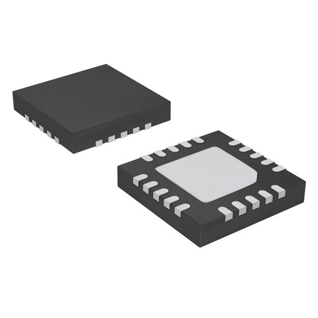
| 产品图片 |
|
| 产品型号 | MCP16251T-I/MNY |
| PWM类型 | 电流模式 |
| rohs | 无铅 / 符合限制有害物质指令(RoHS)规范要求 |
| 产品系列 | - |
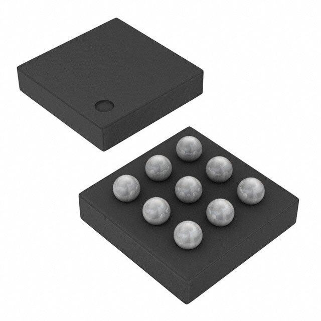
| 供应商器件封装 | 8-TDFN(2x3) |
| 其它名称 | MCP16251T-I/MNYDKR |
| 包装 | Digi-Reel® |
| 同步整流器 | 是 |
| 安装类型 | 表面贴装 |
| 封装/外壳 | 8-WFDFN 裸露焊盘 |
| 工作温度 | -40°C ~ 85°C |
| 标准包装 | 1 |
| 电压-输入 | 0.82 V ~ 6.5 V |
| 电压-输出 | 1.8 V ~ 5.5 V |
| 电流-输出 | 100mA |
| 类型 | 升压(升压) |
| 输出数 | 1 |
| 输出类型 | 可调式 |
| 频率-开关 | 500kHz |


- 商务部:美国ITC正式对集成电路等产品启动337调查
- 曝三星4nm工艺存在良率问题 高通将骁龙8 Gen1或转产台积电
- 太阳诱电将投资9.5亿元在常州建新厂生产MLCC 预计2023年完工
- 英特尔发布欧洲新工厂建设计划 深化IDM 2.0 战略
- 台积电先进制程称霸业界 有大客户加持明年业绩稳了
- 达到5530亿美元!SIA预计今年全球半导体销售额将创下新高
- 英特尔拟将自动驾驶子公司Mobileye上市 估值或超500亿美元
- 三星加码芯片和SET,合并消费电子和移动部门,撤换高东真等 CEO
- 三星电子宣布重大人事变动 还合并消费电子和移动部门
- 海关总署:前11个月进口集成电路产品价值2.52万亿元 增长14.8%


PDF Datasheet 数据手册内容提取
MCP16251/2 Low Quiescent Current, PFM/PWM Synchronous Boost Regulator with True Output Disconnect or Input/Output Bypass Option Features Applications • Up to 96% Typical Efficiency • One, Two and Three-Cell Alkaline and NiMH/NiCd • 650 mA Typical Peak Input Current Limit: Portable Products - I > 100 mA @ 3.3V V , 1.2V V • Solar Cell Applications OUT OUT IN - I > 250 mA @ 3.3V V , 2.4V V • Personal Care and Medical Products OUT OUT IN - I > 225 mA @ 5.0V V , 3.3V V • Bias for Status LEDs OUT OUT IN • Low Device Quiescent Current: • Smartphones, MP3 Players, Digital Cameras - Output Quiescent Current: < 4 µA typical, • Remote Controllers, Portable Instruments device is not switching (V > V , • Wireless Sensors OUT IN excluding feedback divider current) • Bluetooth Headsets - Input Sleep Current: 1 µA • +3.3V to +5.0V Distributed Power Supply - No Load Input Current: 14 µA typical • Shutdown Current: 0.6 µA typical General Description • Low Start-Up Voltage: 0.82V, 1 mA load The MCP16251/2 is a compact, high-efficiency, fixed • Low Operating Input Voltage: down to 0.35V frequency, synchronous step-up DC-DC converter. • Adjustable Output Voltage Range: 1.8V to 5.5V This family of devices provides an easy-to-use power • Maximum Input Voltage V < 5.5V supply solution for applications powered by either OUT • Automatic PFM/PWM Operation: one-cell, two-cell or three-cell alkaline, NiCd, NiMH, one-cell Li-Ion or Li-Polymer batteries. - PWM Operation: 500 kHz - PFM Output Ripple: 150 mV typical Low-voltage technology allows the regulator to start-up without high inrush current or output voltage overshoot • Feedback Voltage: 1.23V from a low-voltage input. High efficiency is • Internal Synchronous Rectifier accomplished by integrating the low-resistance • Internal Compensation N-Channel boost switch and synchronous P-Channel • Inrush Current Limiting and Internal Soft Start switch. All compensation and protection circuitry are (1.5 ms typical) integrated to minimize external components. • Selectable, Logic Controlled, Shutdown States: MCP16251/2 operates and consumes less than 14 µA from battery after start-up, while operating at no load - True Load Disconnect Option (MCP16251) (V = 3.3V, V = 1.5V). The devices provide a true - Input-to-Output Bypass Option (MCP16252) OUT IN disconnect from input to output (MCP16251) or an • Anti-Ringing Control input-to-output bypass (MCP16252), while in shutdown • Overtemperature Protection (EN = GND). Both shutdown options consume less • Available Packages: than 0.6 µA from battery. - SOT-23, 6-Lead Output voltage is set by a small external resistor - TDFN, 2 x 3 x 0.8 mm, 8-Lead divider. Two package options, SOT-23, 6-lead and TDFN, 2 x 3 x 0.8 mm, 8-lead are available. Package Types MCP16251/2 MCP16251/2 6-Lead SOT-23 2x3x0.8 TDFN* SW 1 6 VIN VFB 1 8 VIN GND 2 5 VOUTSGND 2 EP 7 VOUTS 9 P 3 6 V EN 3 4 V GND OUTP FB EN 4 5 SW * Includes Exposed Thermal Pad (EP); see Table 3-1. 2013 - 2016 Microchip Technology Inc. DS20005173B-page 1
MCP16251/2 Typical Application L 4.7µH V OUT VIN 3.3V / 75 mA SW 0.9Vto1.7V VOUT R V TOP IN 1.69M + CIN COUT 4.7µF EN VFB 10µF ne RBOT ali k 1M Al - GND L 4.7µH V OUT VIN 5.0V / 200 mA SW 3.0Vto4.2V VOUTS R V TOP IN V OUTP 3.09M + CIN COUT 4.7µF EN VFB 10µF R n BOT o Li-I 1M - PGND SGND 100 95 V = 3.0V IN 90 ) % 85 ( V = 2.4V y 80 V = 1.5V IN c IN n e 75 i c fi 70 f E 65 60 55 V = 3.3V OUT 50 0.1 1 10 100 1000 I (mA) OUT DS20005173B-page 2 2013 - 2016 Microchip Technology Inc.
MCP16251/2 1.0 ELECTRICAL † Notice: Stresses above those listed under “Maximum CHARACTERISTICS Ratings” may cause permanent damage to the device. This is a stress rating only and functional operation of Absolute Maximum Ratings † the device at those or any other conditions above those indicated in the operational sections of this EN, VFB, VIN, VSW, VOUT - GND.........................+6.5V specification is not intended. Exposure to maximum EN, V .........< maximum V or V > (GND - 0.3V) rating conditions for extended periods may affect FB OUT IN Output Short-Circuit Current......................Continuous device reliability. Output Current Bypass Mode...........................400 mA Power Dissipation ............................Internally Limited Storage Temperature.........................-65°C to +150°C Ambient Temp. with Power Applied......-40°C to +85°C Operating Junction Temperature........-40°C to +125°C ESD Protection On All Pins: HBM...............................................................4 kV MM................................................................400V DC CHARACTERISTICS Electrical Characteristics: Unless otherwise indicated, V = 1.5V, C = C = 10 µF, L = 4.7 µH, V = 3.3V, IN OUT IN OUT I = 0 mA, T = +25°C. Boldface specifications apply over the T range of -40°C to +85°C. OUT A A Parameters Sym. Min. Typ. Max. Units Conditions Input Characteristics Minimum Start-Up Voltage V — 0.82 — V Note 1 IN Minimum Input Voltage V — 0.35 — V Note 1 After Start-Up IN Output Voltage Adjust V V V 1.8 — 5.5 V OUT IN Range OUT Note 2 150 — 1.2V V , 2.0V V IN OUT Maximum Output Current I 100 125 — mA 1.5V V , 3.3V V OUT IN OUT 225 — 3.3V V , 5.0V V IN OUT Feedback Voltage V 1.1931 1.23 1.2669 V FB Feedback Input I — 10 — nA Bias Current VFB I = 0 mA, device is not OUT switching, EN = V = 4.0V, IN V Quiescent Current I — 4.0 8 µA V = 5.0V, does not OUT QOUT OUT include feedback divider current (Note 3) I = 0 mA, EN = V V Sleep Current I — 1.0 2.3 µA OUT IN IN QIN (Note 3), (Note 5) I = 0 mA, No Load Input Current I — 14 25 µA OUT IN0 device is switching V = EN = GND; Quiescent Current – OUT I — 0.6 — µA includes N-Channel and Shutdown QSHDN P-Channel Switch Leakage Note 1: 3.3 k resistive load, 3.3V (1 mA). OUT 2: For V > V , V will not remain in regulation. IN OUT OUT 3: I is measured at V V is supplied externally for V > V (device is not switching), I is QOUT OUT, OUT OUT IN QIN measured at V pin during Sleep period, no load. IN 4: 220 resistive load, 3.3V (15 mA). OUT 5: Determined by characterization, not production tested. 2013 - 2016 Microchip Technology Inc. DS20005173B-page 3
MCP16251/2 DC CHARACTERISTICS (CONTINUED) Electrical Characteristics: Unless otherwise indicated, V = 1.5V, C = C = 10 µF, L = 4.7 µH, V = 3.3V, IN OUT IN OUT I = 0 mA, T = +25°C. Boldface specifications apply over the T range of -40°C to +85°C. OUT A A Parameters Sym. Min. Typ. Max. Units Conditions V = V = 5V IN SW NMOS Switch Leakage I — 0.15 — µA V = 5.5V NLK OUT V = V = GND EN FB V = V = GND PMOS Switch Leakage I — 0.15 — µA IN SW PLK V = 5.5V OUT NMOS Switch V = 3.3V R — 0.45 — IN ON Resistance DS(ON)N I = 100 mA SW PMOS Switch V = 3.3V R — 0.9 — IN ON Resistance DS(ON)P I = 100 mA SW NMOS Peak I — 650 — mA Note 5 Switch Current Limit N(MAX) Includes Line and Load V Accuracy V % -3 — +3 % OUT OUT Regulation; V = 1.5V IN (V /V ) V = 1.5V to 2.8V Line Regulation OUT OUT -0.4 0.3 0.4 %/V IN /V I = 50 mA IN OUT I = 25 mA to 100 mA Load Regulation V /V -1.5 0.1 1.5 % OUT OUT OUT V = 1.5V IN Maximum Duty Cycle DC 87 89 91 % Note 5 MAX Switching Frequency f 425 500 575 kHz SW EN Input Logic High V 70 — — % of V I = 1 mA IH IN OUT EN Input Logic Low V — — 20 % of V I = 1 mA IL IN OUT EN Input Leakage Current I — 5.0 — nA V = 5V ENLK EN EN Low to High Soft Start Time tSS — — 1.5 ms 90% of VOUT (Note 4), (Note 5) Thermal Shutdown I = 20 mA T — 160 — C OUT Die Temperature SD V > 1.4V IN Die Temperature T — 20 — C Hysteresis SDHYS Note 1: 3.3 k resistive load, 3.3V (1 mA). OUT 2: For V > V , V will not remain in regulation. IN OUT OUT 3: I is measured at V V is supplied externally for V > V (device is not switching), I is QOUT OUT, OUT OUT IN QIN measured at V pin during Sleep period, no load. IN 4: 220 resistive load, 3.3V (15 mA). OUT 5: Determined by characterization, not production tested. TEMPERATURE SPECIFICATIONS Electrical Characteristics: Unless otherwise indicated, V = 1.5V, C = C = 10 µF, L = 4.7 µH, V = 3.3V, I = 0 mA. IN OUT IN OUT OUT Parameters Sym. Min. Typ. Max. Units Conditions Temperature Ranges Operating Temperature Range T -40 — +85 °C Steady State J Storage Temperature Range T -65 — +150 °C A Maximum Junction Temperature T — — +150 °C Transient J Package Thermal Resistances Thermal Resistance, SOT-23, 6-LD — 190.5 — °C/W EIA/JESD51-3 Standard JA Thermal Resistance, TDFN, 2x3x0.8m, 8-LD — 52.5 — °C/W JA DS20005173B-page 4 2013 - 2016 Microchip Technology Inc.
MCP16251/2 2.0 TYPICAL PERFORMANCE CURVES Note: The graphs and tables provided following this note are a statistical summary based on a limited number of samples and are provided for informational purposes only. The performance characteristics listed herein are not tested or guaranteed. In some graphs or tables, the data presented may be outside the specified operating range (e.g., outside specified power supply range) and therefore outside the warranted range. Note: Unless otherwise indicated, V = EN = 1.5V, C = C = 10 µF, L = 4.7 µH, V = 3.3V, I = 0 mA, IN OUT IN OUT LOAD T = +25°C, SOT-23 package. A 10 100 VOUT= 3.3V 95 VOUT= 2.0V uA) 8 RRTBOOPT== 11..609 M M(cid:525)(cid:525) 90 urrent ( 6 ncy (%) 8805 C e 75 cent 4 Effici 70 VIN= 1.5V ss 65 uie 2 60 VIN= 1.2V Q 55 VIN= 0.9V 0 50 -40 -25 -10 5 20 35 50 65 80 1 10 100 1000 Ambient Temperature (°C) IOUT(mA) FIGURE 2-1: V I vs. Ambient FIGURE 2-4: 2.0V V Efficiency vs. OUT Q OUT Temperature. I . OUT 30 100 µA)25 RVOTOUPT== 31..36V9 M(cid:525) 95 VOUT= 3.3V nt ( R BOT= 1.0 M(cid:525) 90 ad Input Curre112050 VIN= 1.2V VIN= 1.5V Efficiency (%) 77880505 VIN= 1.2VVIN= 2.5V Lo VIN= 3.0V 65 No 5 60 VIN= 0.9V 0 55 -40 -30 -20 -10 0 10 20 30 40 50 60 70 80 1 10 100 1000 Ambient Temperature (°C) I (mA) OUT FIGURE 2-2: No Load Input Current vs. FIGURE 2-5: 3.3V V Efficiency vs. OUT Temperature. I . OUT 35 100 A)30 RBOT= 1.0 M(cid:525) 95 VOUT= 5.0V ent (µ25 %)90 VIN= 3.6V d Input Curr112050 VOUT= 5.0V Efficiency (788505 VIN= 1.2V VINV=IN 1=.8 2V.5V a o 70 No L 5 VOUT= 2.0V VOUT= 3.3V 65 0 60 1 1.5 2 2.5 3 3.5 4 4.5 1 10 100 1000 Input Voltage (V) I (mA) OUT FIGURE 2-3: No Load Input Current vs. FIGURE 2-6: 5.0V V Efficiency vs. OUT V , after Start-Up. I . IN OUT 2013 - 2016 Microchip Technology Inc. DS20005173B-page 5
MCP16251/2 Note: Unless otherwise indicated, V = EN = 1.5V, C = C = 10 µF, L = 4.7 µH, V = 3.3V, I = 0 mA, IN OUT IN OUT LOAD T = +25°C, SOT-23 package. A 3.33 500 450 V = 5.0V OUT 3.32 A)400 VOUT= 3.3V Voltage (V)33..3301 ILOADILO=A 1D0= m 1 AmA Current (m233505000 VOUT= 2.0V ut d 200 tput33.2299 ILOAD= 50 mA Loa150 O 100 3.28 50 3.27 0 -40 -25 -10 5 20 35 50 65 80 0.9 1.2 1.5 1.8 2.1 2.4 2.7 3 3.3 3.6 3.9 4.2 4.5 Ambient Temperature (°C) Input Voltage (V) FIGURE 2-7: 3.3V V vs. Ambient FIGURE 2-10: Maximum I vs. V , after OUT OUT IN Temperature. Start-up, V Maximum 5% below Regulation OUT Point. 3.32 510 3.31 VIN= 1.2V Hz)505 k e (V)3.30 VIN= 1.5V ncy (500 g e495 put Volta33..2289 ng Frequ448950 utOu3.27 VVIN== 22.44VV hiwitch480 3.26 VIN= 0.9V S475 ILOAD= 20 mA 3.25 470 -40 -25 -10 5 20 35 50 65 80 -40 -25 -10 5 20 35 50 65 80 Ambient Temperature (°C) Ambient Temperature (°C) FIGURE 2-8: 3.3V V vs. Ambient FIGURE 2-11: F vs. Ambient OUT OSC Temperature. Temperature. 3.33 1.2 3.32 TA= +85°C 1.1 VOUT= 3.3V ----ERleescitsrtoivneic L Looaadd, CC Output Voltage (V)3333....22338901 TTAA== +-4205°°CC nput Voltage (V)In 000..8918 ILOAD= 20 mA 3.27 0.7 ILOAD= 1 mA 3.26 ILOAD= 50 mA 0.6 1.51.61.71.81.9 2 2.12.22.32.42.52.62.72.8 -40 -25 -10 5 20 35 50 65 80 Input Voltage (V) Ambient Temperature (°C) FIGURE 2-9: 3.3V V vs. V . FIGURE 2-12: V Start-Up vs. OUT IN IN Temperature into Resistive Load and Constant Current. DS20005173B-page 6 2013 - 2016 Microchip Technology Inc.
MCP16251/2 Note: Unless otherwise indicated, V = EN = 1.5V, C = C = 10 µF, L = 4.7 µH, V = 3.3V, I = 0 mA, IN OUT IN OUT LOAD T = +25°C, SOT-23 package. A 8 1.3 VOUT=1.8V s) 7 m h V) 1.1 O 6 P -Channel e ( e ( g c 5 put Volta 00..79 Startup Resistan 34 n h h I 0.5 Shutdown witc 2 N -Channel S 1 0.3 0 0 10 20 30 40 50 60 70 80 90 0.9 1.2 1.5 1.8 2.1 2.4 2.7 3 3.3 3.6 3.9 4.2 Load Current (mA) > V or V IN OUT FIGURE 2-13: 1.8V Minimum Start-Up FIGURE 2-16: N-Channel and P-Channel OUT and Shutdown V into Resistive Load vs. I . R vs. the Maximum V or V . IN OUT DSON IN OUT 45 1.3 VOUT= 3.3V 40 Voltage (V)01..91 Startup urrent (mA)233505 VOUT= 2.0V VOUT= 3.3V VOUT= 5.0V Input 0.7 ad CLo2105 0.5 Shutdown 10 0.3 5 0 10 20 30 40 50 60 70 80 90 100 0.8 1.2 1.6 2 2.4 2.8 3.2 3.6 4 4.4 Load Current (mA) Input Voltage (V) FIGURE 2-14: 3.3V Minimum Start-Up FIGURE 2-17: Average of PFM-to-PWM OUT and Shutdown V into Resistive Load vs. I . Threshold Current vs. V . IN OUT IN I =1mA OUT 1.7 VOUT= 5.0V 1.5 V) V 100mV/div ge ( 1.3 AOCU CToupled a Volt 1.1 Startup VSW ut 0.9 2 V/div p n I 0.7 0.5 Shutdown 0.3 0 10 20 30 40 50 60 70 80 90 100 IL 100mA/div Load Current (mA) 200µs/div FIGURE 2-15: 5.0V Minimum Start-Up FIGURE 2-18: MCP16251 3.3V V PFM OUT OUT and Shutdown V into Resistive Load vs. I . Mode Waveforms. IN OUT 2013 - 2016 Microchip Technology Inc. DS20005173B-page 7
MCP16251/2 Note: Unless otherwise indicated, V = EN = 1.5V, C = C = 10 µF, L = 4.7 µH, V = 3.3V, I = 0 mA, IN OUT IN OUT LOAD T = +25°C, SOT-23 package. A VOUT 50mV/div IOUT=50mA ISTEP=1mA to 75mA AC Coupled PFM Mode PWM Mode V 100mV/div OUT AC Coupled V SW 2V/div IOUT 50mA/div I 200mA/div L 2µs/div 400µs/div FIGURE 2-19: MCP16251 3.3V V FIGURE 2-22: MCP16251 3.3V V Load OUT OUT PWM Mode Waveforms. Transient Waveforms. IOUT=15mA IOUT=20mA V =3.3V OUT V =1.5V IN V from 1V to 2.5V STEP V IN 1V/div V EN 2V/div V 100mV/div OUT AC Coupled V 2V/div OUT 400µs/div 1ms/div FIGURE 2-20: 3.3V Start-up after Enable. FIGURE 2-23: 3.3V V Line Transient OUT Waveforms. I =15mA I =0mA OUT OUT V 2V/div OUT V 100mV/div OUT AC Coupled V = EN IN 1V/div I 100mA/div I 20mA/div L L 400µs/div 100ms/div FIGURE 2-21: 3.3V Start-Up when FIGURE 2-24: MCP16251 3.3V No Load V = V . V PFM Mode Output Ripple. IN ENABLE OUT DS20005173B-page 8 2013 - 2016 Microchip Technology Inc.
MCP16251/2 3.0 PIN DESCRIPTIONS The descriptions of the pins are listed in Table 3-1. TABLE 3-1: PIN FUNCTION TABLE MCP16251/2 MCP16251/2 Symbol Description SOT-23 TDFN 2x3x0.8 4 1 V Feedback Voltage Pin FB — 2 S Signal Ground Pin GND — 3 P Power Ground Pin GND 3 4 EN Enable Control Input Pin 1 5 SW Switch Node, Boost Inductor Input Pin — 6 V Output Voltage Power Pin OUTP — 7 V Output Voltage Sense Pin OUTS 6 8 V Input Voltage Pin IN — 9 EP Exposed Thermal Pad (EP); must be connected to S and P GND GND. 2 — GND Ground Pin 5 — V Output Voltage Pin OUT 3.1 Feedback Voltage Pin (V ) 3.6 Output Voltage Power Pin (V ) FB OUTP The V pin is used to provide output voltage regulation The output voltage power pin connects the output volt- FB by using a resistor divider. Feedback voltage will age to the switch node. High current flows through the typically be 1.23V, with the output voltage in regulation. integrated P-Channel and out of this pin to the output capacitor and output. In the 2x3x0.8 TDFN package, 3.2 Signal Ground Pin (SGND) VOUTS and VOUTP are connected externally. The signal ground pin is used as a return for the 3.7 Output Voltage Sense Pin (V ) OUTS integrated V and error amplifier. In the 2x3x0.8 REF The output voltage sense pin connects the regulated TDFN package, the S and power ground (P ) GND GND output voltage to the internal bias circuits. In the pins are connected externally. 2x3x0.8 TDFN package, V and V are OUTS OUTP 3.3 Power Ground Pin (P ) connected externally. GND The power ground pin is used as a return for the 3.8 Power Supply Input Voltage Pin (V ) IN high-current N-Channel switch. In the 2x3x0.8 TDFN package, the PGND and signal ground (SGND) pins are Connect the input voltage source to VIN. The input connected externally. source should be decoupled to GND with a 4.7 µF minimum capacitor. 3.4 Enable Pin (EN) 3.9 Exposed Thermal Pad (EP) The EN pin is a logic-level input used to enable or There is no internal electrical connection between the disable device switching and lower quiescent current Exposed Thermal Pad (EP) and the PGND and SGND while disabled. A logic high (>70% of V ) will enable pins. They must be connected to the same potential on IN the regulator output. A logic low (<20% of V ) will the Printed Circuit Board (PCB). IN ensure that the regulator is disabled. 3.10 Ground Pin (GND) 3.5 Switch Node Pin (SW) The ground or return pin is used for circuit ground Connect the inductor from the input voltage to the SW connection. Length of trace from input cap return, pin. The SW pin carries inductor current and can be as output cap return and GND pin should be made as high as 650 mA typical peak. The integrated short as possible to minimize noise on the GND pin. In N-Channel switch drain and integrated P-Channel the SOT23-6 package, a single ground pin is used. switch source are internally connected at the SW node. 3.11 Output Voltage Pin (V ) OUT The output voltage pin connects the integrated P-Channel MOSFET to the output capacitor. The feedback voltage divider is also connected to the V OUT pin for voltage regulation. 2013 - 2016 Microchip Technology Inc. DS20005173B-page 9
MCP16251/2 4.0 DETAILED DESCRIPTION 4.1.2 TRUE OUTPUT DISCONNECT OPTION 4.1 Device Overview The MCP16251 device incorporates a true output disconnect feature. With the EN pin pulled low, the The MCP16251/2 family of devices is capable of low output of the MCP16251 is isolated or disconnected start-up voltage and delivers high efficiency over a wide from the input by turning off the integrated P-Channel load range for single-cell, two-cell, three-cell alkaline, switch and removing the switch bulk diode connection. NiMH, NiCd and single-cell Li-Ion battery inputs. A high This removes the DC path typical in boost converters, level of integration lowers total system cost, eases which allows the output to be disconnected from the implementation and reduces board area. The devices input. During this mode, less than 0.6 µA of current is feature low quiescent current, low start-up voltage, consumed from the input (battery). True output discon- adjustable output voltage, PWM/PFM mode operation, nect does not discharge the output; the output voltage integrated synchronous switch, internal compensation, is held up by the external C capacitance. low noise anti-ring control, inrush current limit and soft OUT start. There are two options for the MCP16251/2 family: 4.1.3 INPUT BYPASS OPTION True Output Disconnect and Input-to-Output Bypass (see Table 4-1). The MCP16252 device incorporates the input-to-output bypass shutdown option. With the EN input pulled low, 4.1.1 PFM/PWM OPERATION the output is connected to the input using the internal P-Channel MOSFET. In this mode, the current draw The MCP16251/2 devices use an automatic switchover from the input (battery) is less than 0.6 µA with no load. from PWM to PFM mode for light load conditions, to The Input Bypass mode is used when the input voltage maximize efficiency over a wide range of output range is high enough for the load to operate in Standby current. During PFM mode, a controlled peak current is or Low I mode. When a higher regulated output used to pump the output up to the threshold limit. While Q voltage is necessary to operate the application, the EN operating in PFM or PWM mode, the P-Channel switch input is pulled high, enabling the boost converter. is used as a synchronous rectifier, turning off when the inductor current reaches 0 mA to maximize efficiency. In this mode, the current through the P-Channel In PFM mode, a comparator is used to terminate MOSFET must not be higher than 400 mA. switching when the output voltage reaches the upper TABLE 4-1: PART NUMBER SELECTION threshold limit. Once switching has terminated, the output voltage will decay or coast down. During this Part True Output Input-to-Output period, which is called Sleep period, 1 µA is typically Number Disconnect Bypass consumed from the input source, which keeps power MCP16251 ✓ — efficiency high at light load. PWM/PFM mode has higher output ripple voltage than PWM mode, and MCP16252 — ✓ variable frequency. The PFM mode frequency is a function of input voltage, output voltage and load. While in PFM mode, the boost converter periodically pumps the output with a fixed switching frequency of 500 kHz. Figure 2-17 represents the load current versus input voltage for the PFM-to-PWM threshold. DS20005173B-page 10 2013 - 2016 Microchip Technology Inc.
MCP16251/2 4.2 Functional Description Figure 4-1 represents the functional block diagram of the MCP16251/2. The MCP16251/2 is a compact, high-efficiency, fixed frequency, step-up DC-DC converter that provides an easy-to-use power supply solution for applications powered by either one-cell, two-cell, or three-cell alkaline, NiCd, or NiMH, or one-cell Li-Ion or Li-Polymer batteries. V OUT Internal V IN BIAS I + ZERO Direction - Control SW SOFT-START .3V 0V Gate Drive II and - LLIIMMIITT EN Shutdown + Control Logic I + SENSE - Slope GND Oscillator S Compensation PWM/PFM + Logic - + 1.23V - V FB EA FIGURE 4-1: MCP16251/2 Block Diagram. 2013 - 2016 Microchip Technology Inc. DS20005173B-page 11
MCP16251/2 4.2.1 LOW-VOLTAGE START-UP In PWM operation, the MCP16251/2 operates as a fixed frequency, synchronous boost converter. The The MCP16251/2 is capable of starting from a low input switching frequency is internally maintained with a pre- voltage. Start-up voltage is typically 0.82V for a 3.3V cision oscillator, typically set to 500 kHz. By operating output and 1 mA resistive load. in PWM-only mode, the output ripple remains low and When enabled, the internal start-up logic turns the the frequency is constant. rectifying P-Channel switch on until the output capacitor is charged to a value close to the input Lossless current sensing converts the peak current voltage. The rectifying switch is current limited during signal to a voltage to sum with the internal slope this time. After charging the output capacitor to the compensation signal. This summed signal is compared input voltage, the device starts switching. If the output to the voltage error amplifier output to provide a peak voltage is below 60-70% of the desired V , the current control command for the PWM signal. The OUT device runs in open-loop with a fixed duty cycle of slope compensation is adaptive to the input and output 70-75% until the output reaches this threshold. During voltage. Therefore, the converter provides the proper start-up, the inductor peak current is limited (see amount of slope compensation to ensure stability, but is Figure 2-21) to allow a correct start from a weak power not excessive, which causes a loss of phase margin. supply, such as a solar cell, small coin battery or a The peak current limit is set to 650 mA typical. discharged battery. Once the output voltage reaches 4.2.3 ADJUSTABLE OUTPUT VOLTAGE 60-70% of the desired V , normal closed-loop PWM OUT operation is initiated. AND MAXIMUM OUTPUT CURRENT The MCP16251/2 charges an internal capacitor with a The MCP16251/2 output voltage is adjustable with a very weak current source. The voltage on this capaci- resistor divider over a 1.8V minimum-to-5.5V maximum tor, in turn, slowly ramps the current limit of the boost range. High value resistors are recommended to mini- switch to its nominal value. The soft-start capacitor is mize quiescent current to keep efficiency high at light completely discharged in the event of a commanded loads. When an application runs below -20°C, smaller shutdown or a thermal shutdown. values for feedback resistors should be used to avoid There is no undervoltage lockout feature for the any alteration of V , because of the leakage path on OUT MCP16251/2. The device will start switching at the PCBs. lowest voltage possible, and run down to the lowest The maximum device output current is dependent on possible voltage. For a minimum 0.82V typical input, the input and output voltage. For example, to ensure a the device starts with regulated output under 1 mA 100 mA load current for V = 3.3V, a minimum of OUT resistive load. Real world loads are mostly 1.1 – 1.2V input voltage is necessary. If an application non-resistive and allow device start-up at lower values, is powered by one Li-Ion battery (V from 3.0V to IN down to 0.65V. Working at very low input voltages may 4.2V), the maximum load current the MCP16251/2 can result in “motor-boating” for deeply discharged deliver is close to 200 mA at 5.0V output (refer to batteries. Figure 2-10). 4.2.2 PFM/PWM MODE 4.2.4 ENABLE The MCP16251/2 devices are capable of automatically The enable pin is used to turn the boost converter on operating in normal PWM mode and PFM mode to and off. The enable threshold voltage varies with input maintain high efficiency at all loads. In PFM mode, the voltage. To enable the boost converter, the EN voltage output ripple has a variable frequency component that level must be greater than 70% of the V voltage. To IN changes with the input voltage and output current. The disable the boost converter, the EN voltage must be value of the output capacitor changes the low lower than 20% of the V voltage. IN frequency component ripple. Output ripple peak-to-peak values are not affected by the output 4.2.5 INTERNAL BIAS capacitor. With no load, the input current drawn from The MCP16251/2 gets its start-up bias from V . Once the battery is typically 14 µA. The device itself is IN the output exceeds the input, bias comes from the powering from the output after start-up, the quiescent output. Therefore, once started, operation is current drawn from output being less than 4 µA (typical, completely independent of V . Operation is limited without feedback resistors divider current). IN only by the output power level and the input source PFM operation is initiated if the output load current falls series resistance. Once started, the output will remain below an internally programmed threshold. The output in regulation down to 0.35V input with 1 mA output voltage is continuously monitored. When the output current for low source impedance inputs. voltage drops below its nominal value, PFM operation pulses once or several times to bring the output back into regulation. If the output load current rises above the upper threshold, the MCP16251/2 enters smoothly into PWM mode. DS20005173B-page 12 2013 - 2016 Microchip Technology Inc.
MCP16251/2 4.2.6 INTERNAL COMPENSATION The error amplifier, with its associated compensation network, completes the closed-loop system by comparing the output voltage to a reference at the input of the error amplifier, and feeding the amplified and inverted signal to the control input of the inner current loop. The compensation network provides phase leads and lags at appropriate frequencies to cancel excessive phase lags and leads of the power circuit. All necessary compensation and slope com- pensation components are integrated. 4.2.7 SHORT-CIRCUIT PROTECTION Unlike most boost converters, the MCP16251/2 allows its output to be shorted during normal operation. The internal current limit and overtemperature protection limit excessive stress and protect the device during periods of short circuit, overcurrent and overtemperature. While operating in Input-to-Output Bypass mode, the P-Channel current limit is inhibited to minimize quiescent current. 4.2.8 LOW NOISE OPERATION The MCP16251/2 integrates a low noise anti-ring switch that damps the oscillations typically observed at the switch node of a boost converter when operating in Discontinuous Inductor Current mode. This removes the high frequency radiated noise. 4.2.9 OVERTEMPERATURE PROTECTION Overtemperature protection circuitry is integrated in the MCP16251/2 devices. This circuitry monitors the device junction temperature and shuts the output off if the junction temperature exceeds the typical +160°C. If this threshold is exceeded, the device will automatically restart once the junction temperature drops by 20°C. During thermal shutdown, the device is periodically checking temperature; once the temperature of the die drops, the device restarts. Because the device takes its bias from the output (to achieve lower I current) while Q in thermal shutdown state, there is no low reference band gap and the output may be higher than zero for inputs below 1.4V typical. The soft start is reset during an overtemperature condition. 2013 - 2016 Microchip Technology Inc. DS20005173B-page 13
MCP16251/2 5.0 APPLICATION INFORMATION The internal error amplifier is a transconductance type, i.e., its gain is not related to the resistors’ value. There are some potential issues with higher value resistors. 5.1 Typical Applications For small surface mount resistors, environment con- The MCP16251/2 synchronous boost regulator tamination can create leakage paths that significantly operates over a wide input and output voltage range. change the resistor divider ratio and change the output The power efficiency is high for several decades of load voltage tolerance. Designers should use resistors that range. Output current capability increases with the are larger than 1 M with precaution; they can be used input voltage and decreases with the increasing output on limited temperature range (-20 to +85oC). For a voltage. The maximum output current is based on the lower temperature (down to -40oC), resistors from N-Channel peak current limit. Typical characterization Examples 1 or 2 should be calculated as follows: curves in this data sheet are presented to display the typical output current capability. EXAMPLE 4: 5.2 Adjustable Output Voltage VOUT = 2.0V Calculations VFB = 1.23V R = 309 k BOT To calculate the resistor divider values for the R = 193.44 kwith a standard value of MCP16251/2, use Equation 5-1, where R is TOP TOP 191 k V is 1.99V) connected to V , R is connected to GND and OUT OUT BOT both are connected to the V input pin. FB EXAMPLE 5: EQUATION 5-1: V = 3.3V OUT V V = 1.23V OUT FB R = R ------------- –1 TOP BOT V RBOT = 309 k FB R = 520.024 kwith a standard value of TOP 523 k V is 3.311V) OUT EXAMPLE 1: Smaller feedback resistor values will increase the V = 2.0V quiescent current drained from the battery by a few µA, OUT but will result in good regulation over the entire V = 1.23V FB temperature range. R = 1 M BOT For boost converters, the removal of the feedback R = 626.01 kwith a standard value of TOP resistors during operation must be avoided. In this 620 k, V is 1.992V) OUT case, the output voltage will increase above the absolute maximum output limits of the MCP16251/2 EXAMPLE 2: and damage the device (for additional information, see Application Note AN1337, “Optimizing Battery Life in V = 3.3V OUT DC Boost Converters Using MCP1640”, DS01337. V = 1.23V FB R = 1 M 5.3 Input Capacitor Selection BOT R = 1.68 Mwith a standard value of TOP The boost input current is smoothed by the boost 1.69 M V is 3.308V) OUT inductor, reducing the amount of filtering necessary at the input. Some capacitance is recommended to EXAMPLE 3: provide decoupling from the source. Low ESR X5R or X7R are well suited, since they have a low temperature V = 5.0V OUT coefficient and small size. For most applications, VFB = 1.23V 4.7 µF of capacitance is sufficient at the input. For R = 1 M high-power applications that have high-source BOT impedance or long leads connecting the battery to the R = 3.065 M (with a standard value of TOP input, 10 µF of capacitance is recommended. 3.09 M V is 5.03V) OUT Additional input capacitance can be added to provide a stable input voltage. Refer to Table 5-1 for the recommended range of the input capacitor value. DS20005173B-page 14 2013 - 2016 Microchip Technology Inc.
MCP16251/2 5.4 Output Capacitor Selection 5.5 Inductor Selection The output capacitor helps provide a stable output The MCP16251/2 is designed to be used with small voltage during sudden load transients and reduces the surface mount inductors; the inductance value can output voltage ripple. As with the input capacitor, X5R range from 2.2 µH to 6.8 µH. An inductance value of and X7R ceramic capacitors are well suited for this 4.7 µH is recommended to achieve a good balance application. Using other capacitor types (aluminum or between the inductor size, converter load transient tantalum) with large ESR has impact on the converter's response and minimized noise. efficiency (see AN1337) and maximum output power. TABLE 5-2: MCP16251/2 RECOMMENDED The MCP16251/2 is internally compensated, so the INDUCTORS output capacitance range is limited. See Table 5-1 for the recommended output capacitor range. Part Value DCR ISAT Size Number (µH) (typ.) (A) WxLxH (mm) An output capacitance higher than 10 µF adds a better load step response and high-frequency noise Coiltronics® attenuation, especially while stepping from light current SD3112 4.7 0.246 0.80 3.1x3.1x1.2 loads (PFM mode) to heavy current loads (PWM SD3114 4.7 0.251 1.14 3.1x3.1x1.4 mode). A minimum of 20 µF output capacitance is mandatory while the output drives load steps between SD3118 4.7 0.162 1.31 3.8x3.8x1.2 heavy load levels. In addition, 2 x 10 µF output SD25 4.7 0.0467 1.83 5.0x5.0x2.5 capacitors ensure a better recovery of the output after Wurth Elektronik a short period of overloading. WE-TPC 4.7 0.100 1.7 2.8x2.8x2.8 While the N-Channel switch is ON, the output current is Type Tiny supplied by the output capacitor C . The amount of OUT WE-TPC 4.7 0.200 0.8 2.8x2.8x1.35 output capacitance and equivalent series resistance Type TH will have a significant effect on the output ripple voltage. While C provides load current, a voltage WE-TPC 4.7 0.105 0.90 3.8x3.8x1.65 OUT drop also appears across its internal ESR that results Type S in ripple voltage. WE-TPC 4.7 0.082 1.65 4.8x4.8x1.8 Type M EQUATION 5-2: Sumida Corporation dV CMD4D06 4.7 0.216 0.75 3.5x4.3x2 I = C ------- OUT OUT dt CDRH4D 4.7 0.09 0.800 4.6x4.6x1.5 Where: Coilcraft dV = Ripple voltage XPL2010 4.7 0.336 0.75 1.9x2x1.0 dt = ON time of the N-Channel switch ME3220 4.7 0.190 1.5 2.5x3.2x2.0 (D x 1/FSW, D is duty cycle) XFL3010 4.7 0.217 1.1 3x3x1.0 XFL3012 4.7 0.143 1.0 3x3x1.2 Table 5-1 contains the recommended range for the input and output capacitor values. EPL3012 4.7 0.165 1.0 3x3x1.3 LPS4018 4.7 0.125 1.8 4x4x1.8 TABLE 5-1: CAPACITOR VALUE RANGE XFL4020 4.7 0.052 2.0 4x4x2.1 C C IN OUT TDK Corporation Minimum 4.7 µF 10 µF VLS3015ET 4.7 0.113 1.1 3x3x1.5 Maximum none 47 µF -4R7M B82462 4.7 0.04 1.8 6x6x3 G4472M B82462 4.7 0.08 2.8 6x6x3 A4472M 2013 - 2016 Microchip Technology Inc. DS20005173B-page 15
MCP16251/2 Several parameters are used to select the inductor As the battery discharges, its deliverable energy or correctly: maximum rated current, saturation current capacity decreases and the internal resistance and copper resistance (ESR). For boost converters, the increases. For example, the internal resistance of an inductor current can be much higher than the output alkaline cell goes up to 1 when discharged causing a current. The lower the inductor ESR, the higher the voltage drop of up to hundreds of mV on the battery efficiency of the converter, a common trade-off in size terminals under load conditions. This aspect will result versus efficiency. in the converter’s inability to start-up properly in applications which require short periods of ON time and The saturation current typically specifies a point at long periods of Sleep. When the load is removed, the which the inductance has rolled off a percentage of the battery voltage slowly recovers. These long cycles may rated value. This can range from a 20-to-40% reduction bring the battery voltage close to its nominal value. in inductance. As the inductance rolls off, the inductor However, a nearly depleted battery will not be capable ripple current increases, as does the peak switch of maintaining its voltage once the heavier load is current. It is important to keep the inductance from applied during the next cycle. At each attempt, the rolling off too much, causing switch current to reach the converter drains a large amount of current to restart peak limit. (see Figure 2-21), weakening the battery even further. As the battery voltage recovers in time, the converter 5.6 One-Cell Application will try to start-up as soon as its minimum input Considerations voltage-vs.-load condition is reached. The MCP16251/2 was designed to operate with a wide In conclusion, with a battery discharged down to its input voltage range after start-up, down to 0.35V, to FEP, a boost converter may start-up and work well accommodate a large variety of input sources. When under light load (in PFM mode), but will stop or lose considering a primary power solution for a design, the regulation when a high load current is required. battery type and load current needs must be carefully selected. 1.6 2000 mAh NiMH The MCP16251/2 start-up voltage is typical 0.82V at 1.5 ----- AA Alkaline 1 mA load but this does not act as an UVLO start-up 1.4 e threshold. The start-up sequence is detailed in g1.3 a Section 4.2.1 “Low-Voltage Start-up” and begins olt1.2 V wcinoiptnhus tt tavhonelt t accghuear.rr egTnihnte g u dnoetfvi l itchtehe e s otaouruttpstpu dutr ta civanopinlatgac gicteou rr reeaqntu ta litmols ibtteihades, Battery 1.11 IBATTERY= 200 mA I = 100 mA 0.9 BATTERY its internal circuitry before the 0.82V input and cannot start-up or operate well with high-impedance sources 0.8 because their voltage varies in time, from zero to over 0.7 0.82V (i.e., energy harvesting). Start-up voltage is the 0 5 10 15 20 25 Run Time (h) point where the device starts switching in closed loop FIGURE 5-1: Example of a Typical and the output is regulated and depends on load and Constant-Current Load Discharge Profile for an temperature as shown in Figures 2-12, 2-13 and 2-14. Alkaline and NiMH Cell. There are a few aspects to deal with when designing a step-up converter supplied from one alkaline or rechargeable cell. Batteries are available in a variety of 200 mV/div sizes and chemistries and can support a variety of VBATTERY = 1.25V VBATTERY = 1.09V drain rates. EN Turn ON/OFF No matter the chemistry, most batteries have several things in common. They should not be drained below EN 1V/div their specified FEP (Functional End Point or Cut-Off VOUT 1V/div IL = Boost Inductor Current Voltage). Below this point, if the battery has a load IL 200 mV/div IBATTERY = Average of IL applied to it, there will not be enough energy to deliver power because all usable capacity is used. For an Boost Converter Load = 100 mA alkaline cell, FEP is 0.9V or 0.8V. Using the alkaline cell Boost Converter Load = 100 mA below the FEP will increase the risk of leakage. There FIGURE 5-2: MCP16251 is an exception for alkaline batteries: if the battery 3.3V /100 mA Boost Converter Waveforms OUT voltage is strictly monitored, it can be drained down to Powered from One Alkaline Cell Discharged to 0.5V in one-cell applications only. For a rechargeable 1.25V Open Load Voltage (Cell Internal NiMH cell, the FEP value is usually 1.0V – 1.1V. Resistance Is Approximately 0.7 Ohms). DS20005173B-page 16 2013 - 2016 Microchip Technology Inc.
MCP16251/2 Another particular situation is powering a boost circuit EQUATION 5-4: from one rechargeable cell like NiMH or NiCd. These R +R applications need an external MCU to monitor the cell 1 2 ULVO 0.4------------------------ voltage or a separate UVLO circuit to prevent deep STOP R 1 discharging, which results in permanent cell damage. where: In a multi-cell powered application (e.g., 2.4V typ. from two NiMH cells) deep discharging will result in a 0.4 is V for selected M resistors range. EBQ1 reverse polarity charging of one of the cells due the It increases to 0.6 if resistors are in k range. unbalanced cell voltages, thus damaging the respective cell. 5.6.1 UVLO CIRCUIT FOR SINGLE-CELL 5.7 Thermal Calculations APPLICATIONS The MCP16251/2 is available in two different packages In single-cell battery applications, it is not always (SOT-23-6 and 2x3x0.8 TDFN-8). By calculating the possible to monitor the start-up and shut-down power dissipation and applying the package thermal voltages using a MCU (due to MCU’s features or to I/O resistance ( ), the junction temperature is estimated. JA pin count limitations). The maximum continuous junction temperature rating One simple way to implement a ULVO circuit is a for the MCP16251/2 family of devices is +125°C. simple diode placed between the V pin (with anode) IN To quickly estimate the internal power dissipation for and EN pin (with cathode) and a bias resistor from EN the switching boost regulator, an empirical calculation to GND. using measured efficiency can be used. Given the Another example which shows an additional ultra low measured efficiency, the internal power dissipation is power undervoltage lockout (UVLO) circuit with Start estimated by Equation 5-5. and Stop thresholds is shown in Figure 5-3. Both thresholds are programmable (1.15V to start and 0.8V EQUATION 5-5: to stop the converter functionality) and new values can be easily calculated using Equations 5-3 and 5-4. The VOUTIOUT ------------------------------- –V I = P UVLO circuit consumes 0.5 µA up to max. 2 µA from Efficiency OUT OUT Dis one battery. The difference between the first term, input power, and to VIN the second term, power delivered, is the internal R MCP16251/2 power dissipation. This is an estimate 1 2.4M which assumes that most of the power lost is internal to + Q1 the MCP16251/2 and not to the CIN, COUT and/or the aline 2RM2 MMBT2907 to EN ibnodousctt oinr.d Tuhcetorer, isw sitohm vee prye rlcitetlnet algoess o fi np otwhee r ilnopsut tin a thned k output capacitors. For a more accurate estimation of Al internal power dissipation, subtract the I 2 x L - INRMS ESR R 3 power dissipation. 2.2MMMBT22Q222 R4 R5 3M 1M 5.8 PCB Layout Information Good printed circuit board layout techniques are FIGURE 5-3: UVLO Circuit Example of a important to any switching circuitry, and switching Low Voltage Boost Converter with 1.15V Start power supplies are no different. When wiring the and 0.8V Stop Thresholds. switching high current paths, short and wide traces should be used. Therefore, it is important that the input EQUATION 5-3: and output capacitors be placed as close as possible to R +R + R the MCP16251/2 to minimize the loop area. 1 2 3 ULVO 0.4------------------------------------- START R The feedback resistors and feedback signal should be 1 routed away from the switching node and the switching current loop. When possible, ground planes and traces should be used to help shield the feedback signal and minimize noise and magnetic interference. 2013 - 2016 Microchip Technology Inc. DS20005173B-page 17
MCP16251/2 Via to GND Plane R R BOT TOP +V +V IN OUT C C L IN MCP16251/2 OUT 1 GND GND Via for Enable FIGURE 5-4: MCP16251/2 SOT-23-6 Recommended Layout. Wired on Bottom L Plane +V IN +V OUT C C IN OUT GND MCP16251/2 R TOP 1 R BOT Enable GND FIGURE 5-5: MCP16251/2 TDFN-8 Recommended Layout. DS20005173B-page 18 2013 - 2016 Microchip Technology Inc.
MCP16251/2 6.0 TYPICAL APPLICATION CIRCUITS L 1 4.7µH MCP16252 VOUT Manganese Lithium 5.0V@5mA Dioxide Button Cell SW V OUT V IN + 3.09M 2.0V to 3.2V CIN COUT - 4.7µF EN VFB 10µF 1M From PIC® MCU I/O GND Note: For applications that can operate directly from the battery input voltage during Standby mode and require a higher voltage during Normal Run mode, the MCP16252 device provides input-to-output bypass, when disabled. Here, the PIC® microcontroller is powered by the output of the MCP16252. One of the microcontroller’s I/O pins is used to enable and disable the MCP16252, and to control its bias voltage. While in Shutdown mode, the MCP16252 input current is typically 0.6 µA. FIGURE 6-1: Manganese Lithium Coin Cell Application using I/O Bypass Mode. L 4.7µH R1 MCP16251 VOUT 2.4M SW 3.3V + Q1 VIN VOUT RTOP aline R2 MMBT2907 1.69M COUT k 2M Al EN VFB 10µF R BOT - R 1M 3 CIN 2.2M Q2 4.7µF MMBT2222 R4 R5 GND 3.09M 1M Note: This is a simple low I one-cell boost converter Q with an external ULVO circuit. The EN pin is kept VIN high as long as the battery voltage is higher than EN 0.8V. The converter will not (re)start if the battery voltage is lower than 1.1V and will stop working (EN goes low level) if battery voltage drops below 0.8V. The external ULVO circuit consumes approximately 0.5 µA from a discharged battery and max. 2 µA from a fresh battery. R +R +R 1 2 3 ULVO = 0.4--------------------------------------- START R 1 R +R 1 2 ULVO = 0.4------------------------- STOP R 1 FIGURE 6-2: MCP16251 with an External ULVO Circuit. 2013 - 2016 Microchip Technology Inc. DS20005173B-page 19
MCP16251/2 V L MCP16251 OUT Load Switch 3.3V Q2 4.7µH SW NDS332 VBATT VOUT VIN OUT 1.3M C IN 4.7µF 1M VFB + Alkalineor NIMH Cell EN GND 240kC10OUµTF Drive EN Q1 - NDS7002 GP2 1k V Sensing GP4 GP1 OUT 510k V BATT Sensing 1µF V MCU Bias from VOUT DD 220k Weak Up GP3/MCLR GP0 ON / OFF PIC12F617 VSS Drive Load Switch Note: Application example for a simple low I one-cell boost converter attached to a PIC® MCU to monitor Q battery and output converter voltages and drive a load switch. When battery is connected, EN is pulled high by a 1 M resistor and the converter starts regulating V , biasing the PIC MCU. The push button OUT is used to switch on and off the load switch and put the PIC MCU in Deep Sleep mode. Battery energy is saved during the time when no power is needed for the load by pulsing the EN pin with low frequency to keep the output in a 2.3-to-3.3V range for the V pin of the PIC MCU. A detailed description of this DD application can be found in the “MCP1640 Single Quadruple-A Battery Boost Converter Reference Design”, (DS51922) and in application note AN1337, “Optimizing Battery Life in DC Boost Converters Using MCP1640”, (DS01337). FIGURE 6-3: Application showing a PIC® MCU attached to the MCP16251 to help optimize battery life, and monitor the battery and output voltages. DS20005173B-page 20 2013 - 2016 Microchip Technology Inc.
MCP16251/2 7.0 PACKAGING INFORMATION 7.1 Package Marking Information 6-Lead SOT-23 Example: Part Number Code MB25 MCP16251T-I/CH MBNN MCP16252T-I/CH MCNN 8-Lead TDFN (2x3x0.8) Example: Part Number Code ABP MCP16251T-I/MNY ABP MCP16252T-I/MNY ABQ Legend: XX...X Customer-specific information Y Year code (last digit of calendar year) YY Year code (last 2 digits of calendar year) WW Week code (week of January 1 is week ‘01’) NNN Alphanumeric traceability code e3 Pb-free JEDEC designator for Matte Tin (Sn) * This package is Pb-free. The Pb-free JEDEC designator ( e 3 ) can be found on the outer packaging for this package. Note: In the event the full Microchip part number cannot be marked on one line, it will be carried over to the next line, thus limiting the number of available characters for customer-specific information. 2013 - 2016 Microchip Technology Inc. DS20005173B-page 21
MCP16251/2 (cid:2)(cid:3)(cid:4)(cid:5)(cid:6)(cid:7)(cid:8)(cid:9)(cid:10)(cid:6)(cid:11)(cid:12)(cid:13)(cid:14)(cid:8)(cid:15)(cid:16)(cid:6)(cid:10)(cid:10)(cid:8)(cid:17)(cid:18)(cid:12)(cid:10)(cid:13)(cid:19)(cid:5)(cid:8)(cid:20)(cid:21)(cid:6)(cid:19)(cid:11)(cid:13)(cid:11)(cid:12)(cid:22)(cid:21)(cid:8)(cid:23)(cid:24)(cid:25)(cid:26)(cid:8)(cid:27)(cid:15)(cid:17)(cid:20)(cid:3)(cid:28)(cid:29)(cid:30) (cid:31)(cid:22)(cid:12)(cid:5)! /(cid:23)(cid:22)(cid:14)$(cid:24)(cid:13)(cid:14) (cid:23)!$(cid:14)(cid:21)%(cid:22)(cid:22)(cid:13)(cid:26)$(cid:14)(cid:10)(cid:11)(cid:21)0(cid:11)(cid:12)(cid:13)(cid:14)"(cid:22)(cid:11).(cid:20)(cid:26)(cid:12)!1(cid:14)(cid:10)(cid:27)(cid:13)(cid:11)!(cid:13)(cid:14)!(cid:13)(cid:13)(cid:14)$(cid:24)(cid:13)(cid:14)(cid:19)(cid:20)(cid:21)(cid:22)(cid:23)(cid:21)(cid:24)(cid:20)(cid:10)(cid:14)2(cid:11)(cid:21)0(cid:11)(cid:12)(cid:20)(cid:26)(cid:12)(cid:14)(cid:3)(cid:10)(cid:13)(cid:21)(cid:20)&(cid:20)(cid:21)(cid:11)$(cid:20)(cid:23)(cid:26)(cid:14)(cid:27)(cid:23)(cid:21)(cid:11)$(cid:13)"(cid:14)(cid:11)$(cid:14) (cid:24)$$(cid:10),33...(cid:30) (cid:20)(cid:21)(cid:22)(cid:23)(cid:21)(cid:24)(cid:20)(cid:10)(cid:30)(cid:21)(cid:23) 3(cid:10)(cid:11)(cid:21)0(cid:11)(cid:12)(cid:20)(cid:26)(cid:12) b N 4 E E1 PIN1IDBY LASERMARK 1 2 3 e e1 D A A2 c φ L A1 L1 4(cid:26)(cid:20)$! (cid:19)(cid:29)55(cid:29)(cid:19)#(cid:25)#(cid:8)(cid:3) (cid:2)(cid:20) (cid:13)(cid:26)!(cid:20)(cid:23)(cid:26)(cid:14)5(cid:20) (cid:20)$! (cid:19)(cid:29)6 67(cid:19) (cid:19)(cid:7)8 6% 9(cid:13)(cid:22)(cid:14)(cid:23)&(cid:14)2(cid:20)(cid:26)! 6 (cid:16) 2(cid:20)$(cid:21)(cid:24) (cid:13) (cid:4)(cid:30)(cid:6))(cid:14)*(cid:3)+ 7%$!(cid:20)"(cid:13)(cid:14)5(cid:13)(cid:11)"(cid:14)2(cid:20)$(cid:21)(cid:24) (cid:13)(cid:31) (cid:31)(cid:30)(cid:6)(cid:4)(cid:14)*(cid:3)+ 7-(cid:13)(cid:22)(cid:11)(cid:27)(cid:27)(cid:14):(cid:13)(cid:20)(cid:12)(cid:24)$ (cid:7) (cid:4)(cid:30)(cid:6)(cid:4) ; (cid:31)(cid:30)(cid:5)) (cid:19)(cid:23)(cid:27)"(cid:13)"(cid:14)2(cid:11)(cid:21)0(cid:11)(cid:12)(cid:13)(cid:14)(cid:25)(cid:24)(cid:20)(cid:21)0(cid:26)(cid:13)!! (cid:7)(cid:17) (cid:4)(cid:30)<(cid:6) ; (cid:31)(cid:30)(cid:15)(cid:4) (cid:3)$(cid:11)(cid:26)"(cid:23)&& (cid:7)(cid:31) (cid:4)(cid:30)(cid:4)(cid:4) ; (cid:4)(cid:30)(cid:31)) 7-(cid:13)(cid:22)(cid:11)(cid:27)(cid:27)(cid:14)=(cid:20)"$(cid:24) # (cid:17)(cid:30)(cid:17)(cid:4) ; (cid:15)(cid:30)(cid:17)(cid:4) (cid:19)(cid:23)(cid:27)"(cid:13)"(cid:14)2(cid:11)(cid:21)0(cid:11)(cid:12)(cid:13)(cid:14)=(cid:20)"$(cid:24) #(cid:31) (cid:31)(cid:30)(cid:15)(cid:4) ; (cid:31)(cid:30)<(cid:4) 7-(cid:13)(cid:22)(cid:11)(cid:27)(cid:27)(cid:14)5(cid:13)(cid:26)(cid:12)$(cid:24) (cid:2) (cid:17)(cid:30)(cid:18)(cid:4) ; (cid:15)(cid:30)(cid:31)(cid:4) /(cid:23)(cid:23)$(cid:14)5(cid:13)(cid:26)(cid:12)$(cid:24) 5 (cid:4)(cid:30)(cid:31)(cid:4) ; (cid:4)(cid:30)(cid:16)(cid:4) /(cid:23)(cid:23)$(cid:10)(cid:22)(cid:20)(cid:26)$ 5(cid:31) (cid:4)(cid:30)(cid:15)) ; (cid:4)(cid:30)<(cid:4) /(cid:23)(cid:23)$(cid:14)(cid:7)(cid:26)(cid:12)(cid:27)(cid:13) (cid:3) (cid:4)> ; (cid:15)(cid:4)> 5(cid:13)(cid:11)"(cid:14)(cid:25)(cid:24)(cid:20)(cid:21)0(cid:26)(cid:13)!! (cid:21) (cid:4)(cid:30)(cid:4)< ; (cid:4)(cid:30)(cid:17)(cid:16) 5(cid:13)(cid:11)"(cid:14)=(cid:20)"$(cid:24) 9 (cid:4)(cid:30)(cid:17)(cid:4) ; (cid:4)(cid:30))(cid:31) (cid:31)(cid:22)(cid:12)(cid:5)(cid:11)! (cid:31)(cid:30) (cid:2)(cid:20) (cid:13)(cid:26)!(cid:20)(cid:23)(cid:26)!(cid:14)(cid:2)(cid:14)(cid:11)(cid:26)"(cid:14)#(cid:31)(cid:14)"(cid:23)(cid:14)(cid:26)(cid:23)$(cid:14)(cid:20)(cid:26)(cid:21)(cid:27)%"(cid:13)(cid:14) (cid:23)(cid:27)"(cid:14)&(cid:27)(cid:11)!(cid:24)(cid:14)(cid:23)(cid:22)(cid:14)(cid:10)(cid:22)(cid:23)$(cid:22)%!(cid:20)(cid:23)(cid:26)!(cid:30)(cid:14)(cid:19)(cid:23)(cid:27)"(cid:14)&(cid:27)(cid:11)!(cid:24)(cid:14)(cid:23)(cid:22)(cid:14)(cid:10)(cid:22)(cid:23)$(cid:22)%!(cid:20)(cid:23)(cid:26)!(cid:14)!(cid:24)(cid:11)(cid:27)(cid:27)(cid:14)(cid:26)(cid:23)$(cid:14)(cid:13)’(cid:21)(cid:13)(cid:13)"(cid:14)(cid:4)(cid:30)(cid:31)(cid:17)(cid:18)(cid:14) (cid:14)(cid:10)(cid:13)(cid:22)(cid:14)!(cid:20)"(cid:13)(cid:30) (cid:17)(cid:30) (cid:2)(cid:20) (cid:13)(cid:26)!(cid:20)(cid:23)(cid:26)(cid:20)(cid:26)(cid:12)(cid:14)(cid:11)(cid:26)"(cid:14)$(cid:23)(cid:27)(cid:13)(cid:22)(cid:11)(cid:26)(cid:21)(cid:20)(cid:26)(cid:12)(cid:14)(cid:10)(cid:13)(cid:22)(cid:14)(cid:7)(cid:3)(cid:19)#(cid:14)((cid:31)(cid:5)(cid:30))(cid:19)(cid:30) *(cid:3)+, *(cid:11)!(cid:20)(cid:21)(cid:14)(cid:2)(cid:20) (cid:13)(cid:26)!(cid:20)(cid:23)(cid:26)(cid:30)(cid:14)(cid:25)(cid:24)(cid:13)(cid:23)(cid:22)(cid:13)$(cid:20)(cid:21)(cid:11)(cid:27)(cid:27)(cid:28)(cid:14)(cid:13)’(cid:11)(cid:21)$(cid:14)-(cid:11)(cid:27)%(cid:13)(cid:14)!(cid:24)(cid:23).(cid:26)(cid:14).(cid:20)$(cid:24)(cid:23)%$(cid:14)$(cid:23)(cid:27)(cid:13)(cid:22)(cid:11)(cid:26)(cid:21)(cid:13)!(cid:30) (cid:19)(cid:20)(cid:21)(cid:22)(cid:23)(cid:21)(cid:24)(cid:20)(cid:10)(cid:25)(cid:13)(cid:21)(cid:24)(cid:26)(cid:23)(cid:27)(cid:23)(cid:12)(cid:28)(cid:2)(cid:22)(cid:11).(cid:20)(cid:26)(cid:12)+(cid:4)(cid:5)(cid:9)(cid:4)(cid:17)<* DS20005173B-page 22 2013 - 2016 Microchip Technology Inc.
MCP16251/2 Note: For the most current package drawings, please see the Microchip Packaging Specification located at http://www.microchip.com/packaging 2013 - 2016 Microchip Technology Inc. DS20005173B-page 23
MCP16251/2 8-Lead Plastic Dual Flat, No Lead Package (MNY) – 2x3x0.8 mm Body [TDFN] With 1.4x1.3 mm Exposed Pad (JEDEC Package type WDFN) Note: For the most current package drawings, please see the Microchip Packaging Specification located at http://www.microchip.com/packaging D A B N (DATUM A) (DATUM B) E NOTE 1 2X 0.15 C 1 2 2X 0.15 C TOP VIEW 0.10 C (A3) C A SEATING PLANE 8X A1 0.08 C SIDE VIEW 0.10 C A B D2 L 1 2 0.10 C A B NOTE 1 E2 K N 8X b e 0.10 C A B 0.05 C BOTTOM VIEW Microchip Technology Drawing No. C04-129-MNY Rev E Sheet 1 of 2 DS20005173B-page 24 2013 - 2016 Microchip Technology Inc.
MCP16251/2 8-Lead Plastic Dual Flat, No Lead Package (MNY) – 2x3x0.8 mm Body [TDFN] With 1.4x1.3 mm Exposed Pad (JEDEC Package type WDFN) Note: For the most current package drawings, please see the Microchip Packaging Specification located at http://www.microchip.com/packaging Units MILLIMETERS Dimension Limits MIN NOM MAX Number of Pins N 8 Pitch e 0.50 BSC Overall Height A 0.70 0.75 0.80 Standoff A1 0.00 0.02 0.05 Contact Thickness A3 0.20 REF Overall Length D 2.00 BSC Overall Width E 3.00 BSC Exposed Pad Length D2 1.35 1.40 1.45 Exposed Pad Width E2 1.25 1.30 1.35 Contact Width b 0.20 0.25 0.30 Contact Length L 0.25 0.30 0.45 Contact-to-Exposed Pad K 0.20 - - Notes: 1. Pin 1 visual index feature may vary, but must be located within the hatched area. 2. Package may have one or more exposed tie bars at ends. 3. Package is saw singulated 4. Dimensioning and tolerancing per ASME Y14.5M BSC: Basic Dimension. Theoretically exact value shown without tolerances. REF: Reference Dimension, usually without tolerance, for information purposes only. Microchip Technology Drawing No. C04-129-MNY Rev E Sheet 2 of 2 2013 - 2016 Microchip Technology Inc. DS20005173B-page 25
MCP16251/2 8-Lead Plastic Dual Flat, No Lead Package (MNY) – 2x3x0.8 mm Body [TDFN] With 1.4x1.3 mm Exposed Pad (JEDEC Package type WDFN) Note: For the most current package drawings, please see the Microchip Packaging Specification located at http://www.microchip.com/packaging X2 EV 8 ØV C Y2 EV Y1 1 2 SILK SCREEN X1 E RECOMMENDED LAND PATTERN Units MILLIMETERS Dimension Limits MIN NOM MAX Contact Pitch E 0.50 BSC Optional Center Pad Width X2 1.60 Optional Center Pad Length Y2 1.50 Contact Pad Spacing C 2.90 Contact Pad Width (X8) X1 0.25 Contact Pad Length (X8) Y1 0.85 Thermal Via Diameter V 0.30 Thermal Via Pitch EV 1.00 Notes: 1. Dimensioning and tolerancing per ASME Y14.5M BSC: Basic Dimension. Theoretically exact value shown without tolerances. 2. For best soldering results, thermal vias, if used, should be filled or tented to avoid solder loss during reflow process Microchip Technology Drawing No. C04-129-MNY Rev. B DS20005173B-page 26 2013 - 2016 Microchip Technology Inc.
MCP16251/2 APPENDIX A: REVISION HISTORY Revision B (September 2016) The following is the list of modifications: • Added Section 5.6 “One-Cell Application Considerations”. • Updated Section 6.0 “Typical Application Circuits”. • Minor typographical corrections Revision A (March 2013) • Original Release of this Document. 2013 - 2016 Microchip Technology Inc. DS20005173B-page 27
MCP16251/2 NOTES: DS20005173B-page 28 2013 - 2016 Microchip Technology Inc.
MCP16251/2 PRODUCT IDENTIFICATION SYSTEM To order or obtain information, e.g., on pricing or delivery, refer to the factory or the listed sales office. PART NO. X -X /XX Examples: a) MCP16251T-I/CH: Tape and Reel Device Tape Temperature Package Industrial Temperature and Reel Range 6LD SOT-23 Package b) MCP16251T-I/MNY: Tape and Reel Industrial Temperature Device: MCP16251T:Low Quiescent Current, PFM/PWM 8LD 2x3 TDFN Package Synchronous Boost Regulator, True Output a) MCP16252T-I/CH: Tape and Reel Disconnect Shutdown Option (Tape and Reel) Industrial Temperature MCP16252T:Low Quiescent Current, PFM/PWM 6LD SOT-23 Package Synchronous Boost Regulator, Input-to-Output b) MCP16252T-I/MNY: Tape and Reel Bypass Shutdown Option (Tape and Reel) Industrial Temperature 8LD 2x3 TDFN Package Temperature Range: I = -40C to +85C (Industrial) Package: CH =Plastic Small Outline Transistor, SOT-23, 6-lead MNY* =Lead Plastic Dual Flat, No Lead Package, 2x3x0.8 mm TDFN, 8-lead *Y =Nickel palladium gold manufacturing designator 2013 - 2016 Microchip Technology Inc. DS20005173B-page 29
MCP16251/2 NOTES: DS20005173B-page 30 2013 - 2016 Microchip Technology Inc.
Note the following details of the code protection feature on Microchip devices: • Microchip products meet the specification contained in their particular Microchip Data Sheet. • Microchip believes that its family of products is one of the most secure families of its kind on the market today, when used in the intended manner and under normal conditions. • There are dishonest and possibly illegal methods used to breach the code protection feature. All of these methods, to our knowledge, require using the Microchip products in a manner outside the operating specifications contained in Microchip’s Data Sheets. Most likely, the person doing so is engaged in theft of intellectual property. • Microchip is willing to work with the customer who is concerned about the integrity of their code. • Neither Microchip nor any other semiconductor manufacturer can guarantee the security of their code. Code protection does not mean that we are guaranteeing the product as “unbreakable.” Code protection is constantly evolving. We at Microchip are committed to continuously improving the code protection features of our products. Attempts to break Microchip’s code protection feature may be a violation of the Digital Millennium Copyright Act. If such acts allow unauthorized access to your software or other copyrighted work, you may have a right to sue for relief under that Act. Information contained in this publication regarding device Trademarks applications and the like is provided only for your convenience The Microchip name and logo, the Microchip logo, AnyRate, and may be superseded by updates. It is your responsibility to dsPIC, FlashFlex, flexPWR, Heldo, JukeBlox, KeeLoq, ensure that your application meets with your specifications. KeeLoq logo, Kleer, LANCheck, LINK MD, MediaLB, MOST, MICROCHIP MAKES NO REPRESENTATIONS OR MOST logo, MPLAB, OptoLyzer, PIC, PICSTART, PIC32 logo, WARRANTIES OF ANY KIND WHETHER EXPRESS OR RightTouch, SpyNIC, SST, SST Logo, SuperFlash and UNI/O IMPLIED, WRITTEN OR ORAL, STATUTORY OR are registered trademarks of Microchip Technology OTHERWISE, RELATED TO THE INFORMATION, Incorporated in the U.S.A. and other countries. INCLUDING BUT NOT LIMITED TO ITS CONDITION, QUALITY, PERFORMANCE, MERCHANTABILITY OR ClockWorks, The Embedded Control Solutions Company, FITNESS FOR PURPOSE. Microchip disclaims all liability ETHERSYNCH, Hyper Speed Control, HyperLight Load, arising from this information and its use. Use of Microchip IntelliMOS, mTouch, Precision Edge, and QUIET-WIRE are devices in life support and/or safety applications is entirely at registered trademarks of Microchip Technology Incorporated the buyer’s risk, and the buyer agrees to defend, indemnify and in the U.S.A. hold harmless Microchip from any and all damages, claims, Analog-for-the-Digital Age, Any Capacitor, AnyIn, AnyOut, suits, or expenses resulting from such use. No licenses are BodyCom, chipKIT, chipKIT logo, CodeGuard, dsPICDEM, conveyed, implicitly or otherwise, under any Microchip dsPICDEM.net, Dynamic Average Matching, DAM, ECAN, intellectual property rights unless otherwise stated. EtherGREEN, In-Circuit Serial Programming, ICSP, Inter-Chip Connectivity, JitterBlocker, KleerNet, KleerNet logo, MiWi, motorBench, MPASM, MPF, MPLAB Certified logo, MPLIB, MPLINK, MultiTRAK, NetDetach, Omniscient Code Generation, PICDEM, PICDEM.net, PICkit, PICtail, PureSilicon, RightTouch logo, REAL ICE, Ripple Blocker, Serial Quad I/O, SQI, SuperSwitcher, SuperSwitcher II, Total Endurance, TSHARC, USBCheck, VariSense, ViewSpan, WiperLock, Wireless DNA, and ZENA are trademarks of Microchip Technology Incorporated in the U.S.A. and other countries. SQTP is a service mark of Microchip Technology Incorporated in the U.S.A. Microchip received ISO/TS-16949:2009 certification for its worldwide headquarters, design and wafer fabrication facilities in Chandler and Silicon Storage Technology is a registered trademark of Tempe, Arizona; Gresham, Oregon and design centers in California Microchip Technology Inc. in other countries. and India. The Company’s quality system processes and procedures are for its PIC® MCUs and dsPIC® DSCs, KEELOQ® code hopping GestIC is a registered trademark of Microchip Technology devices, Serial EEPROMs, microperipherals, nonvolatile memory and Germany II GmbH & Co. KG, a subsidiary of Microchip analog products. In addition, Microchip’s quality system for the design and manufacture of development systems is ISO 9001:2000 certified. Technology Inc., in other countries. All other trademarks mentioned herein are property of their respective companies. QUALITY MANAGEMENT SYSTEM © 2013 - 2016, Microchip Technology Incorporated, Printed in CERTIFIED BY DNV the U.S.A., All Rights Reserved. ISBN: 978-1-5224-0953-3 == ISO/TS 16949 == 2013 - 2016 Microchip Technology Inc. DS20005173B-page 31
Worldwide Sales and Service AMERICAS ASIA/PACIFIC ASIA/PACIFIC EUROPE Corporate Office Asia Pacific Office China - Xiamen Austria - Wels 2355 West Chandler Blvd. Suites 3707-14, 37th Floor Tel: 86-592-2388138 Tel: 43-7242-2244-39 Chandler, AZ 85224-6199 Tower 6, The Gateway Fax: 86-592-2388130 Fax: 43-7242-2244-393 Tel: 480-792-7200 Harbour City, Kowloon China - Zhuhai Denmark - Copenhagen Fax: 480-792-7277 Hong Kong Tel: 86-756-3210040 Tel: 45-4450-2828 Technical Support: Tel: 852-2943-5100 Fax: 86-756-3210049 Fax: 45-4485-2829 http://www.microchip.com/ Fax: 852-2401-3431 India - Bangalore France - Paris support Australia - Sydney Tel: 91-80-3090-4444 Tel: 33-1-69-53-63-20 Web Address: Tel: 61-2-9868-6733 Fax: 91-80-3090-4123 Fax: 33-1-69-30-90-79 www.microchip.com Fax: 61-2-9868-6755 India - New Delhi Germany - Dusseldorf Atlanta China - Beijing Tel: 91-11-4160-8631 Tel: 49-2129-3766400 Duluth, GA Tel: 678-957-9614 Tel: 86-10-8569-7000 Fax: 91-11-4160-8632 Germany - Karlsruhe Fax: 678-957-1455 Fax: 86-10-8528-2104 India - Pune Tel: 49-721-625370 China - Chengdu Tel: 91-20-3019-1500 Germany - Munich Austin, TX Tel: 512-257-3370 Tel: 86-28-8665-5511 Japan - Osaka Tel: 49-89-627-144-0 Fax: 86-28-8665-7889 Tel: 81-6-6152-7160 Fax: 49-89-627-144-44 Boston Westborough, MA China - Chongqing Fax: 81-6-6152-9310 Italy - Milan Tel: 774-760-0087 Tel: 86-23-8980-9588 Japan - Tokyo Tel: 39-0331-742611 Fax: 86-23-8980-9500 Tel: 81-3-6880- 3770 Fax: 39-0331-466781 Fax: 774-760-0088 China - Dongguan Fax: 81-3-6880-3771 Italy - Venice Chicago Itasca, IL Tel: 86-769-8702-9880 Korea - Daegu Tel: 39-049-7625286 Tel: 630-285-0071 China - Guangzhou Tel: 82-53-744-4301 Netherlands - Drunen Fax: 630-285-0075 Tel: 86-20-8755-8029 Fax: 82-53-744-4302 Tel: 31-416-690399 China - Hangzhou Korea - Seoul Fax: 31-416-690340 Cleveland Independence, OH Tel: 86-571-8792-8115 Tel: 82-2-554-7200 Poland - Warsaw Tel: 216-447-0464 Fax: 86-571-8792-8116 Fax: 82-2-558-5932 or Tel: 48-22-3325737 Fax: 216-447-0643 China - Hong Kong SAR 82-2-558-5934 Spain - Madrid Dallas Tel: 852-2943-5100 Malaysia - Kuala Lumpur Tel: 34-91-708-08-90 Addison, TX Fax: 852-2401-3431 Tel: 60-3-6201-9857 Fax: 34-91-708-08-91 Tel: 972-818-7423 China - Nanjing Fax: 60-3-6201-9859 Sweden - Stockholm Fax: 972-818-2924 Tel: 86-25-8473-2460 Malaysia - Penang Tel: 46-8-5090-4654 Fax: 86-25-8473-2470 Tel: 60-4-227-8870 Detroit UK - Wokingham Novi, MI China - Qingdao Fax: 60-4-227-4068 Tel: 44-118-921-5800 Tel: 248-848-4000 Tel: 86-532-8502-7355 Philippines - Manila Fax: 44-118-921-5820 Fax: 86-532-8502-7205 Tel: 63-2-634-9065 Houston, TX Fax: 63-2-634-9069 Tel: 281-894-5983 China - Shanghai Tel: 86-21-5407-5533 Singapore Indianapolis Fax: 86-21-5407-5066 Tel: 65-6334-8870 Noblesville, IN Tel: 317-773-8323 China - Shenyang Fax: 65-6334-8850 Fax: 317-773-5453 Tel: 86-24-2334-2829 Taiwan - Hsin Chu Fax: 86-24-2334-2393 Tel: 886-3-5778-366 Los Angeles Mission Viejo, CA China - Shenzhen Fax: 886-3-5770-955 Tel: 949-462-9523 Tel: 86-755-8864-2200 Taiwan - Kaohsiung Fax: 949-462-9608 Fax: 86-755-8203-1760 Tel: 886-7-213-7828 New York, NY China - Wuhan Taiwan - Taipei Tel: 631-435-6000 Tel: 86-27-5980-5300 Tel: 886-2-2508-8600 Fax: 86-27-5980-5118 Fax: 886-2-2508-0102 San Jose, CA Tel: 408-735-9110 China - Xian Thailand - Bangkok Tel: 86-29-8833-7252 Tel: 66-2-694-1351 Canada - Toronto Fax: 86-29-8833-7256 Fax: 66-2-694-1350 Tel: 905-695-1980 Fax: 905-695-2078 06/23/16 DS20005173B-page 32 2013 - 2016 Microchip Technology Inc.
Mouser Electronics Authorized Distributor Click to View Pricing, Inventory, Delivery & Lifecycle Information: M icrochip: MCP16252T-I/CH MCP16251T-I/CH MCP16251T-I/MNY MCP16252T-I/MNY