ICGOO在线商城 > 集成电路(IC) > PMIC - 稳压器 - DC DC 开关稳压器 > TPS62125DSGT

 Datasheet下载
- 型号: TPS62125DSGT
- 制造商: Texas Instruments
- 库位|库存: xxxx|xxxx
- 要求:
| 数量阶梯 | 香港交货 | 国内含税 |
| +xxxx | $xxxx | ¥xxxx |
查看当月历史价格
查看今年历史价格
TPS62125DSGT产品简介:
ICGOO电子元器件商城为您提供TPS62125DSGT由Texas Instruments设计生产,在icgoo商城现货销售,并且可以通过原厂、代理商等渠道进行代购。 TPS62125DSGT价格参考。Texas InstrumentsTPS62125DSGT封装/规格:PMIC - 稳压器 - DC DC 开关稳压器, Buck Switching Regulator IC Positive Adjustable 1.2V 1 Output 300mA 8-WFDFN Exposed Pad。您可以下载TPS62125DSGT参考资料、Datasheet数据手册功能说明书,资料中有TPS62125DSGT 详细功能的应用电路图电压和使用方法及教程。
TPS62125DSGT是Texas Instruments(德州仪器)推出的一款高效、同步降压型DC-DC开关稳压器,适用于对空间和功耗敏感的便携式电子设备。其典型应用场景包括:

1. 便携式消费类电子产品:如智能手机、平板电脑、智能手表和可穿戴设备。该芯片具有高达2MHz的开关频率,支持使用小型电感和电容,有助于减小整体解决方案尺寸,非常适合紧凑型设计。

2. 电池供电系统:因其高效率(在轻载时可达95%以上)和低静态电流(典型值为30μA),特别适合由单节锂电池供电的设备,能够有效延长电池续航时间。

3. 物联网(IoT)设备:如无线传感器节点、智能家居终端等,这些设备通常要求长时间待机与低功耗运行,TPS62125DSGT的节能模式(PFM)可在轻负载下自动切换,优化能效。

4. FPGA、ASIC及微处理器供电:可为低电压核心逻辑提供稳定的1.8V、3.3V或可调输出电压(0.9V至5.5V),满足多种数字电路的电源需求。

5. 工业与医疗便携设备:如手持仪表、便携式诊断设备等,得益于其良好的热性能和稳定输出(±2%精度),可在宽温范围内可靠工作。

该器件采用小型6引脚DSG(ThinSOT™)封装,便于高密度布局,同时具备过温保护和软启动功能,提升系统安全性。综合来看,TPS62125DSGT是一款适用于高性能、低功耗、小体积电源设计的理想选择。
| 参数 | 数值 |
| 产品目录 | 集成电路 (IC)半导体 |
| 描述 | IC REG BUCK SYNC ADJ 0.3A 8WSON稳压器—开关式稳压器 3V-17V, 300mA Buck Converter |
| DevelopmentKit | TPS62125EVM-044 |
| 产品分类 | |
| 品牌 | Texas Instruments |
| 产品手册 | |
| 产品图片 |
|
| rohs | 符合RoHS无铅 / 符合限制有害物质指令(RoHS)规范要求 |
| 产品系列 | 电源管理 IC,稳压器—开关式稳压器,Texas Instruments TPS62125DSGTDCS-Control™ |
| 数据手册 | |
| 产品型号 | TPS62125DSGT |
| PWM类型 | 混合物 |
| 产品种类 | 稳压器—开关式稳压器 |
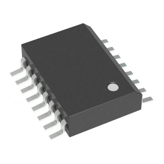
| 供应商器件封装 | 8-WSON (2x2) |
| 其它名称 | 296-30461-1 |
| 包装 | 剪切带 (CT) |
| 同步整流器 | 是 |
| 商标 | Texas Instruments |
| 安装类型 | 表面贴装 |
| 安装风格 | SMD/SMT |
| 封装 | Reel |
| 封装/外壳 | 8-WFDFN 裸露焊盘 |
| 封装/箱体 | WSON-8 |
| 工作温度 | -40°C ~ 85°C |
| 工作温度范围 | - 40 C to + 85 C |
| 工厂包装数量 | 250 |
| 开关频率 | 1 MHz |
| 拓扑结构 | Buck |
| 最大输入电压 | 17 V |
| 最小工作温度 | - 40 C |
| 标准包装 | 1 |
| 电压-输入 | 3 V ~ 17 V |
| 电压-输出 | 1.2 V ~ 10 V |
| 电流-输出 | 300mA |
| 类型 | 降压(降压) |
| 系列 | TPS62125 |
| 设计资源 | http://www.digikey.com/product-highlights/cn/zh/texas-instruments-webench-design-center/3176 |
| 输出数 | 1 |
| 输出电压 | 1.2 V to 10 V |
| 输出电流 | 300 mA |
| 输出端数量 | 1 Output |
| 输出类型 | 可调式 |
| 配用 | /product-detail/zh/TPS62125EVM-044/296-37521-ND/3431144 |
| 频率-开关 | 1MHz |


- 商务部:美国ITC正式对集成电路等产品启动337调查
- 曝三星4nm工艺存在良率问题 高通将骁龙8 Gen1或转产台积电
- 太阳诱电将投资9.5亿元在常州建新厂生产MLCC 预计2023年完工
- 英特尔发布欧洲新工厂建设计划 深化IDM 2.0 战略
- 台积电先进制程称霸业界 有大客户加持明年业绩稳了
- 达到5530亿美元!SIA预计今年全球半导体销售额将创下新高
- 英特尔拟将自动驾驶子公司Mobileye上市 估值或超500亿美元
- 三星加码芯片和SET,合并消费电子和移动部门,撤换高东真等 CEO
- 三星电子宣布重大人事变动 还合并消费电子和移动部门
- 海关总署:前11个月进口集成电路产品价值2.52万亿元 增长14.8%


PDF Datasheet 数据手册内容提取
Product Order Technical Tools & Support & Reference Folder Now Documents Software Community Design TPS62125 SLVSAQ5E–MARCH2012–REVISEDMAY2017 TPS62125 3-V to 17-V, 300-mA Step-Down Converter With Adjustable Enable Threshold and Hysteresis 1 Features 3 Description • WideInputVoltageRange3Vto17V The TPS62125 device is a high-efficiency 1 synchronous step-down converter optimized for low • InputSupplyVoltageSupervisor(SVS)With and ultralow power applications providing up to 300- AdjustableThresholdandHysteresisConsuming mA output current. The wide input voltage range of 3 Typical6-µAQuiescentCurrent V to 17 V supports 4-cell alkaline and 1- to 4-cell Li- • WideOutputVoltageRange1.2Vto10V Ion batteries in series configuration as well as 9-V to 15-V powered applications. The device includes a • Typical13-µAQuiescentCurrent precise low-power enable comparator which can be • 350-nATypicalShutdownCurrent used as an input supply voltage supervisor (SVS) to • SeamlessPowerSaveModeTransition address system specific power-up and power-down • DCS-Control™Scheme requirements. The enable comparator consumes only 6-µA quiescent current and features an accurate • LowOutputRippleVoltage threshold of 1.2 V typical as well as an adjustable • Upto1-MHzSwitchingFrequency hysteresis. With this feature, the converter can • HighestEfficiencyoverWideV andV Range generate a power supply rail by extracting energy IN OUT from a storage capacitor fed from high impedance • PintoPinCompatiblewithTPS62160/70 sources such as solar panels or current loops. With • 100%DutyCycleMode its DCS-Control scheme the converter provides • PowerGoodOpenDrainOutput power-save mode operation to maintain highest • OutputDischargeFunction efficiency over the entire load current range. At light loads the converter operates in pulse frequency • Small2-mm×2-mm8-pinWSONPackage modulation (PFM) mode and transitions seamlessly and automatically in pulse width modulation (PWM) 2 Applications mode at higher load currents. The DCS-Control™ • EmbeddedProcessing scheme is optimized for low-output ripple voltage in PFM mode in order to reduce output noise to a • 4-CellAlkaline,1-to4-CellLi-IonBattery-Powered minimum and features excellent AC load regulation. Applications An open-drain power good output indicates once the • 9-Vto15-VStandbyPowerSupply outputvoltageisinregulation. • EnergyHarvesting DeviceInformation(1) • Inverter(NegativeV ) OUT PARTNUMBER PACKAGE BODYSIZE(NOM) TPS62125 WSON(8) 2.00mm×2.00mm (1) For all available packages, see the orderable addendum at theendofthedatasheet. TypicalApplicationSchematic EfficiencyvsInputVoltage VIN= 4V to 17V TPS62125 L15µH VupOU tTo= 330.30VmA 95 10mA 100mA VIN SW 90 R VOS 1.81M COUT 85 250mA CIN EENN FB 10µF 10µF R 80 1.0mA 2 EN_hys 576k ncy (%)75 e Rpullup Effici70 0.25mA GND PG PWR GOOD 65 V = 3.3V OUT 60 L= 15mH VLF302515 C = 10mF OUT 55 0.1mA 50 4 5 6 7 8 9 10 11 12 13 14 15 16 17 Input Voltage V(V) IN 1 An IMPORTANT NOTICE at the end of this data sheet addresses availability, warranty, changes, use in safety-critical applications, intellectualpropertymattersandotherimportantdisclaimers.PRODUCTIONDATA.
TPS62125 SLVSAQ5E–MARCH2012–REVISEDMAY2017 www.ti.com Table of Contents 1 Features.................................................................. 1 8 ApplicationandImplementation........................ 13 2 Applications........................................................... 1 8.1 ApplicationInformation............................................13 3 Description............................................................. 1 8.2 TypicalApplication..................................................13 4 RevisionHistory..................................................... 2 8.3 SystemExamples ..................................................26 5 PinConfigurationandFunctions......................... 3 9 PowerSupplyRecommendations...................... 28 6 Specifications......................................................... 4 10 Layout................................................................... 28 6.1 AbsoluteMaximumRatings......................................4 10.1 LayoutGuidelines.................................................28 6.2 ESDRatings..............................................................4 10.2 LayoutExample....................................................28 6.3 RecommendedOperatingConditions.......................4 11 DeviceandDocumentationSupport................. 29 6.4 ThermalInformation..................................................4 11.1 DeviceSupport......................................................29 6.5 ElectricalCharacteristics...........................................5 11.2 ReceivingNotificationofDocumentationUpdates29 6.6 TypicalCharacteristics..............................................7 11.3 CommunityResources..........................................29 7 DetailedDescription.............................................. 9 11.4 Trademarks...........................................................29 7.1 Overview...................................................................9 11.5 ElectrostaticDischargeCaution............................29 7.2 FunctionalBlockDiagram.........................................9 11.6 Glossary................................................................29 7.3 FeatureDescription.................................................10 12 Mechanical,Packaging,andOrderable Information........................................................... 29 7.4 DeviceFunctionalModes........................................10 4 Revision History NOTE:Pagenumbersforpreviousrevisionsmaydifferfrompagenumbersinthecurrentversion. ChangesfromRevisionD(July2015)toRevisionE Page • AddedSWnodeACabsmaxratings .................................................................................................................................... 4 ChangesfromRevisionC(December2013)toRevisionD Page • AddedPinConfigurationandFunctionssection,ESDRatingstable,FeatureDescriptionsection,DeviceFunctional Modes,ApplicationandImplementationsection,PowerSupplyRecommendationssection,Layoutsection,Device andDocumentationSupportsection,andMechanical,Packaging,andOrderableInformationsection .............................. 1 2 SubmitDocumentationFeedback Copyright©2012–2017,TexasInstrumentsIncorporated ProductFolderLinks:TPS62125
TPS62125 www.ti.com SLVSAQ5E–MARCH2012–REVISEDMAY2017 5 Pin Configuration and Functions DSGPackage 8-PinWSON TopView GND 1 8 PG VEINN 32 EHXEPROSMEALDPAD 76 SVWOS T EN_hys 4 5 FB PinFunctions PIN I/O DESCRIPTION NAME NO. Inputpinfortheenablecomparator.PullingthispintoGNDturnsthedeviceintoshutdownmode. TheDC/DCconverterisenabledoncetherisingvoltageonthispintripstheenablecomparator threshold,V oftyp.1.2V.TheDC/DCconverteristurnedoffonceafallingvoltageonthis EN 3 IN THENON pintripsthethreshold,V oftyp.1.15V.Thecomparatorthresholdcanbeincreasedby THENOFF connectinganexternalresistortopinEN_hys.Seealsoapplicationsection.Thispinmustbe terminated. Enablehysteresisopen-drainoutput.ThispinispulledtoGNDwhenthevoltageontheENpinis belowthecomparatorthresholdV oftyp.1.2Vandthecomparatorhasnotyettripped.The THENON pinishighimpedanceoncetheenablecomparatorhastrippedandthevoltageatthepinENis EN_hys 4 OUT abovethethresholdV .ThepinispulledtoGNDoncethefallingvoltageontheENpintrips THENON thethresholdV (1.15Vtypical).Thispincanbeusedtoincreasethehysteresisofthe THENOFF enablecomparator.Ifnotused,tiethispintoGND,orleaveitopen. Thisisthefeedbackpinfortheregulator.Anexternalresistordividernetworkconnectedtothispin FB 5 IN setstheoutputvoltage.Incaseoffixedoutputvoltageoption,theresistordividerisintegratedand thepinneedtobeconnecteddirectlytotheoutputvoltage. GND 1 PWR GNDsupplypin. Opendrainpowergoodoutput.ThispinisinternallypulledtoGNDwhenthedeviceisdisabledor theoutputvoltageisbelowthePGthreshold.Thepinisfloatingwhentheoutputvoltageisin regulationandabovethePGthreshold.Forpowergoodindication,thepincanbeconnectedviaa PG 8 OUT pullupresistortoavoltagerailupto10.Thepincansinkacurrentupto0.4mAandmaintainthe specifiedhigh/lowvoltagelevels.Itcanbeusedtodischargetheoutputcapacitorwithupto10mA. Inthiscasethecurrentintothepinmustbelimitedwithanappropriatepullupresistor.Moredetails canbefoundintheapplicationsection.Ifnotused,leavethepinopen,orconnecttoGND. ThisistheswitchpinandisconnectedtotheinternalMOSFETswitches.Connecttheinductorto SW 7 OUT thispin.DonottiethispintoVIN,VOUTorGND. VIN 2 PWR V powersupplypin. IN ThisistheoutputvoltagesensepinfortheDCS-Controlcircuitry.Thispinmustbeconnectedtothe VOS 6 IN outputvoltageoftheDC/DCconverter. Exposed – – ThispadmustbeconnectedtoGND. ThermalPAD Copyright©2012–2017,TexasInstrumentsIncorporated SubmitDocumentationFeedback 3 ProductFolderLinks:TPS62125
TPS62125 SLVSAQ5E–MARCH2012–REVISEDMAY2017 www.ti.com 6 Specifications 6.1 Absolute Maximum Ratings MIN MAX UNIT VIN –0.3 20 V SW(DC) –0.3 V +0.3V V IN SW(AC,lessthan10ns)(3) -3.0 23.5 V Pinvoltage(2) EN –0.3 V +0.3 V IN FB –0.3 3.6 V VOS,PG –0.3 12 V EN_hys –0.3 7 V Powergoodsink I 10 mA PG current EN_hyssinkcurrent I 3 mA EN_hys Maximumoperatingjunctiontemperature,T –40 125 °C J Storagetemperature,T –65 150 °C stg (1) StressesbeyondthoselistedunderAbsoluteMaximumRatingsmaycausepermanentdamagetothedevice.Thesearestressratings onlyandfunctionaloperationofthedeviceattheseoranyotherconditionsbeyondthoseindicatedunderRecommendedOperating Conditionsisnotimplied.Exposuretoabsolute–maximum–ratedconditionsforextendedperiodsmayaffectdevicereliability. (2) AllvoltagevaluesarewithrespecttonetworkgroundterminalGND. (3) Whileswitching 6.2 ESD Ratings VALUE UNIT Humanbodymodel(HBM),perANSI/ESDA/JEDECJS-001(1) ±2000 V Electrostaticdischarge V (ESD) Charged-devicemodel(CDM),perJEDECspecificationJESD22-C101(2) ±1000 (1) JEDECdocumentJEP155statesthat500-VHBMallowssafemanufacturingwithastandardESDcontrolprocess. (2) JEDECdocumentJEP157statesthat250-VCDMallowssafemanufacturingwithastandardESDcontrolprocess. 6.3 Recommended Operating Conditions MIN NOM MAX UNIT V Supplyvoltage 3 17 V IN 3V≤V <6V 200 IN Outputcurrentcapability mA 6V≤V ≤17V 300 IN T Operatingambienttemperature (1)(UnlessOtherwiseNoted) –40 85 °C A T Operatingjunctiontemperature, –40 125 °C J (1) Inapplicationswherehighpowerdissipationand/orpoorpackagethermalresistanceispresent,themaximumambienttemperaturemay havetobederated.Maximumambienttemperature(T )isdependentonthemaximumoperatingjunctiontemperature(T )and A(max) J(max) themaximumpowerdissipationofthedeviceintheapplication(P );formoreinformationabouttraditionalandnewthermalmetrics, D(max) seetheSemiconductorandICPackageThermalMetricsapplicationreport. 6.4 Thermal Information TPS62125 THERMALMETRIC(1) DSG(WSON) UNIT 8PINS R Junction-to-ambientthermalresistance 65.2 °C/W θJA R Junction-to-case(top)thermalresistance 93.3 °C/W θJC(top) R Junction-to-boardthermalresistance 30.1 °C/W θJB ψ Junction-to-topcharacterizationparameter 0.5 °C/W JT ψ Junction-to-boardcharacterizationparameter 47.4 °C/W JB R Junction-to-case(bottom)thermalresistance 7.2 °C/W θJC(bot) (1) Formoreinformationabouttraditionalandnewthermalmetrics,seetheSemiconductorandICPackageThermalMetricsapplication report. 4 SubmitDocumentationFeedback Copyright©2012–2017,TexasInstrumentsIncorporated ProductFolderLinks:TPS62125
TPS62125 www.ti.com SLVSAQ5E–MARCH2012–REVISEDMAY2017 6.5 Electrical Characteristics T =–40°Cto85°C,typicalvaluesareatT =25°C(unlessotherwisenoted),V =12V A A IN PARAMETER TESTCONDITIONS MIN TYP MAX UNIT SUPPLY V Inputvoltagerange(1) 3 17 V IN V Outputvoltagerange 1.2 10 V OUT I =0mA,devicenotswitching,EN=V , OUT IN 13 23 µA regulatorsleeps I =0mA,deviceswitching,V =7.2V, I Quiescentcurrent OUT IN 14 µA Q V =1.2V,L=22µH OUT V =5V,EN=1.1V,enablecomparatoractive, IN 6 11 µA deviceDC/DCconverteroff V =5V=V ,T =25°C,high-sideMOSFET I Activemodecurrentconsumption IN OUT A 230 275 µA Active switchfullyturnedon(100%mode) Enablecomparatoroff,EN<0.4V, I Shutdowncurrent(2) 0.35 2.4 µA SD V =SW=0V,V =5V OUT IN FallingV 2.8 2.85 V IN V Undervoltagelockoutthreshold UVLO RisingV 2.9 2.95 V IN ENABLECOMPARATORTHRESHOLDANDHYSTERESIS(EN,EN_hys) V ENpinthresholdrisingedge 1.16 1.20 1.24 V THENON V ENpinthresholdfallingedge 3V≤V≤17V 1.12 1.15 1.19 V THENOFF V ENpinhysteresis 50 mV THENHys IN I InputbiascurrentintoENpin EN=1.3V 0 50 nA INEN V EN_hyspinoutputlow I =1mA,EN=1.1V 0.4 V EN_hyst EN_hyst I InputbiascurrentintoEN_hystpin EN_hyst=1.3V 0 50 nA INEN_hyst POWERSWITCH V =3V,I=100mA 2.4 4 IN High-sideMOSFETON-resistance V =12V,I=100mA 1.5 2.6 IN R Ω DS(ON) V =3V,I=100mA 0.75 1.3 IN Low-sideMOSFETON-resistance V =12V,I=100mA 0.6 1 IN Switchcurrentlimithigh-side I V =12V 600 750 900 mA LIMF MOSFET IN Thermalshutdown Increasingjunctiontemperature 150 °C T SD Thermalshutdownhysteresis Decreasingjunctiontemperature 20 °C OUTPUT t MinimumON-time V =5V,V =2.5V 500 ns ONmin IN OUT t MinimumOFF-time V =5V 60 ns OFFmin IN Internalreferencevoltageoferror V 0.808 V REF_FB amplifier Feedbackvoltageaccuracy Referredtointernalreference(V ) –2.5% 0% 2.5% REF_FB Feedbackvoltagelineregulation I =100mA,5V≤V ≤17V,V =3.3V(3) –0.05 %/V V OUT IN OUT FB Feedbackvoltageloadregulation V =3.3V;I =1mAto300mA,V =12V(3) –0.00 %/mA OUT OUT IN 4 I InputbiascurrentintoFBpin V =0.8V 0 50 nA IN_FB FB TimefromENhightodevicestartsswitching, t Regulatorstart-uptime 50 Start VIN=5V µs t Outputvoltageramptime TimetorampupV =1.8V,noload 200 Ramp OUT ILK_SW LeakagecurrentintoSWpin(4) VOS=VIN=VSW=1.8V,EN=GND,devicein 1.8 2.85 µA I BiascurrentintoVOSpin shutdownmode 0 50 nA IN_VOS (1) ThepartisfunctionaldowntothefallingUVLO(UndervoltageLockout)threshold (2) CurrentintoVINpin (3) V =3.3V,L=15µH,C =10µF OUT OUT (4) Aninternalresistordividernetworkwithtyp.1MΩtotalresistanceisconnectedbetweenSWpinandGND. Copyright©2012–2017,TexasInstrumentsIncorporated SubmitDocumentationFeedback 5 ProductFolderLinks:TPS62125
TPS62125 SLVSAQ5E–MARCH2012–REVISEDMAY2017 www.ti.com Electrical Characteristics (continued) T =–40°Cto85°C,typicalvaluesareatT =25°C(unlessotherwisenoted),V =12V A A IN PARAMETER TESTCONDITIONS MIN TYP MAX UNIT POWERGOODOUTPUT(PG) RisingV feedbackvoltage 93% 95% 97% FB V Powergoodthresholdvoltage TH_PG FallingV feedbackvoltage 87% 90% 93% FB V PGpinoutputlowvoltage CurrentintoPGpinI =0.4mA 0.3 V OL PG V PGpinoutputhighvoltage Opendrainoutput,externalpullupresistor 10 V OH I BiascurrentintoPGpin V =3V,EN=1.3V,FB=0.85V 0 50 nA IN_PG (PG) 6 SubmitDocumentationFeedback Copyright©2012–2017,TexasInstrumentsIncorporated ProductFolderLinks:TPS62125
TPS62125 www.ti.com SLVSAQ5E–MARCH2012–REVISEDMAY2017 6.6 Typical Characteristics 1.5 25 1.4 1.3 1.2 TA= 85°C 20 Ino switching:T= 85°C 1.1 Q A Shutdown Current - I[A]mSD0000001.......4567890 TTAA=T= A2 05=°° TC-C4A0=° 6C0°C Quiescent Current I(A)mQ1105 Idevice switchiIIInQQQgnnn:oooT sss=www iii2tttccc5hhh°iiiCnnnggg,:::TTTAAA=== 6-24050°°°CCC Q A 0.3 5 V = 1.8V, I = 0mAno load, OUT OUT 0.2 EN = VIN 0.1 0 0 3 4 5 6 7 8 9 10 11 12 13 14 15 16 17 3 4 5 6 7 8 9 10 11 12 13 14 15 16 17 Input Voltage - VIN[V] Input Voltage (V) Figure1.ShutdownCurrentvs.InputVoltage Figure2.QuiescentCurrentvs.InputVoltage 1000 25 20 VIN= 6V TA= 85°C 100 Quiescent Current (A)m10 VVVVVVIIIIIINNNNNN====== 666111VVV222VVV TTT TTTAAAAAA====== 8-2 48−5250°55°4°CC°°0CCC°C Quiescent Current (A)m1105 VVVVVIIIINNNNIN===== 1616 21V2VV2V TTV TTAA TAA==A== -2=4−85 0245°°C50°CC°°CC 1 5 0.1 0 0 200 400 600 800 1000 1200 1400 0 200 400 600 800 1000 1200 1400 Voltage VEN(mV) Voltage VEN(mV) Figure3.QuiescentCurrentvs.ENVoltage,RisingVEN Figure4.QuiescentCurrentvs.VENVoltage,FallingVEN 1.25 3 1.245 2.8 1.24 1.235 2.6 EN ComparatorThreshold - V(V)TH EN111111111111......1112221......111222789012.2789123555555 VVTH EN ONTTA== --4400°°CCVTVH TEHN EONF FONTTAA== 2 255°VVC°CTH EN ONTTA== 8855°°CC R(W)DSON00111122........1268246824 TA= -40°C TA= 0°CTA= 6T0A°=C 25°CTA= 85°C 1.165 TH EN OFF A TH EN OFF A 0.4 1.16 0.2 1.155 1.153 4 5 6 7 8 9 10 11 12 13 14 15 16 17 03 4 5 6 7 8 9 10 11 12 13 14 15 16 17 Input Voltage VIN(V) Input Voltage VIN[V] Figure5.ENComparatorThresholdsvs.InputVoltage Figure6.R High-SideSwitch DSON Copyright©2012–2017,TexasInstrumentsIncorporated SubmitDocumentationFeedback 7 ProductFolderLinks:TPS62125
TPS62125 SLVSAQ5E–MARCH2012–REVISEDMAY2017 www.ti.com Typical Characteristics (continued) 1.0 0.9 0.8 TA= 85°C TA= 60°C 0.7 0.6 W) R(DSON0.5 0.4 0.3 TA= 0°C TA= 25°C TA= -40°C 0.2 0.1 0 3 4 5 6 7 8 9 10 11 12 13 14 15 16 17 Input Voltage - VIN[V] Figure7.R Low-SideSwitch(Rectifier) DSON 8 SubmitDocumentationFeedback Copyright©2012–2017,TexasInstrumentsIncorporated ProductFolderLinks:TPS62125
TPS62125 www.ti.com SLVSAQ5E–MARCH2012–REVISEDMAY2017 7 Detailed Description 7.1 Overview The TPS62125 high-efficiency synchronous switch mode buck converter includes TI's DCS-Control (Direct Control with Seamless Transition into Power-Save Mode), an advanced regulation topology, which combines the advantages of hysteretic and voltage mode control. Characteristics of DCS-Control are excellent AC load regulation and transient response, low-output ripple voltage and a seamless transition between PFM and PWM modeoperation. DCS-Control includes an AC loop which senses the output voltage (VOS pin) and directly feeds the information to a fast comparator stage. This comparator sets the switching frequency, which is constant for steady state operating conditions, and provides immediate response to dynamic load changes. In order to achieve accurate DC load regulation, a voltage feedback loop is used. The internally compensated regulation network achieves fast and stable operation with small external components and low ESR capacitors. The DCS-Control topology supports pulse width modulation (PWM) mode for medium and high load conditions and a power-save mode at light loads. During PWM mode, it operates in continuous conduction. The switch frequency is up to 1 MHz with a controlled frequency variation depending on the input voltage. If the load current decreases, the converter seamless enters power-save mode to maintain high efficiency down to very light loads. In power-save mode the switching frequency varies linearly with the load current. Because DCS-Control supports both operation modes within one single building block, the transition from PWM to power-save mode is seamless without effects on the output voltage. The TPS62125 offers both excellent DC voltage and superior load transient regulation, combined withverylow-outputvoltageripple,minimizinginterferencewithRFcircuits. At high load currents the converter operates in quasi fixed frequency PWM mode operation and at light loads in pulse frequency modulation (PFM) mode to maintain highest efficiency over the full load current range. In PFM mode, the device generates a single switching pulse to ramp up the inductor current and recharge the output capacitor, followed by a sleep period where most of the internal circuits are shutdown to achieve a quiescent current of typically 13 µA. During this time, the load current is supported by the output capacitor. The duration of thesleepperioddependsontheloadcurrentandtheinductorpeakcurrent. 7.2 Functional Block Diagram OSND/ 1V.2REEVFN 0V.8RE0F8_FVB SSofotsfttsatratrt PG Comparator PG UVLO VTH_PG EN Comparator FB VREF VIN EN Comparator VUVLO EN_hys DC-DC EN_comp ON/OFF Peak Current Limit Comparator GND Limit Timer High Side VIN DCConStrol VIN Min. On CLoongtircol PMOS VOS Min. OFF VOS Direct Control Gate Driver & Compensation Anti SW Shoot-Through V REF_FB FB NMOS Error Comparator amplifier GND fixed VOUT Thermal Zero Current Shutdown Comparator Copyright©2012–2017,TexasInstrumentsIncorporated SubmitDocumentationFeedback 9 ProductFolderLinks:TPS62125
TPS62125 SLVSAQ5E–MARCH2012–REVISEDMAY2017 www.ti.com 7.3 Feature Description 7.3.1 UndervoltageLockout In addition to the EN comparator, the device includes an under-voltage lockout circuit which prevents the device from misoperation at low input voltages. Both circuits are fed to an AND gate and prevents the converter from turning on the high-side MOSFET switch or low-side MOSFET under undefined conditions. The UVLO threshold is set to 2.9 V typical for rising V and 2.8 V typical for falling V . The hysteresis between rising and falling IN IN UVLO threshold ensures proper start-up. Fully functional operation is permitted for an input voltage down to the falling UVLO threshold level. The converter starts operation again once the input voltage trips the rising UVLO thresholdlevelandthevoltageattheENpintripsV . TH_EN_ON 7.3.2 EnableComparator(EN/EN_hys) The EN pin is connected to an on/shutdown detector (ON/SD) and an input of the enable comparator. With a voltage level of 0.4 V or less at the EN pin, the ON/SD detector turns the device into Shutdown mode and the quiescent current is reduced to typically 350 nA. In this mode the EN comparator as well the entire internal- control circuitry are switched off. A voltage level of typical 900 mV (rising) at the EN pin triggers the on/shutdown detector and activates the internal reference V (typical 1.2 V), the EN comparator and the UVLO comparator. REF In applications with slow rising voltage levels at the EN pin, the quiescent current profile before this trip point needs to be considered, see Figure 3. Once the ON/SD detector has tripped, the quiescent current consumption of the device is typical 6 µA. The TPS62125 starts regulation once the voltage at the EN pin trips the threshold V (typical 1.2 V) and the input voltage is above the UVLO threshold. It enters softstart and ramps up the EN_TH ON output voltage. For proper operation, the EN pin must be terminated and must not be left floating. The quiescent current consumption of the TPS62125 is typical 13 µA under no load condition (not switching). See Figure 1. The DC/DCregulatorstopsoperationoncethevoltageontheENpinfallsbelowthethresholdV (typical1.15 EN_THOFF V)ortheinputvoltagefallsbelowUVLOthreshold.Theenablecomparatorfeaturesabuiltinhysteresisoftypical 50mV.ThishysteresiscanbeincreasedwithanexternalresistorconnectedtopinEN_hys. 7.3.3 PowerGoodOutputandOutputDischarge(PG) The power good output (PG pin) is an open drain output. The circuit is active once the device is enabled. It is driven by an internal comparator connected to the FB pin voltage and an internal reference. The PG output provides a high level (open drain high impedance) once the feedback voltage exceeds typical 95% of its nominal value. The PG output is driven to low level once the FB pin voltage falls below typical 90% of its nominal value V . The PG output goes high (high impedance) with a delay of typically 2 µs. A pull up resistor is needed to REF_FB generate a high level. The PG pin can be connected via a pull up resistors to a voltage up to 10 V. This pin can alsobeusedtodischargetheoutputcapacitor.SeesectionApplicationInformationformoredetails. The PG output is pulled low if the voltage on the EN pin falls below the threshold V or the input voltage EN_TH OFF isbelowtheundervoltagelockoutthresholdUVLO. 7.3.4 ThermalShutdown As soon as the junction temperature, T , exceeds 150°C (typical) the device goes into thermal shutdown. In this J mode, the high-side and low-side MOSFETs are turned-off. The device continues its operation when the junction temperaturefallsbelowthethermalshutdownhysteresis. 7.4 Device Functional Modes 7.4.1 PulseWidthModulation(PWM)Operation The TPS62125 operates with pulse width modulation in continuous conduction mode (CCM) with a nominal switching frequency of about 1 MHz. The frequency variation in PWM mode is controlled and depends on V , IN V and the inductance. The device operates in PWM mode as long the output current is higher than half the OUT inductor's ripple current. To maintain high efficiency at light loads, the device enters power-save mode at the boundary to discontinuous conduction mode (DCM). This happens if the output current becomes smaller than halftheinductor'sripplecurrent. 10 SubmitDocumentationFeedback Copyright©2012–2017,TexasInstrumentsIncorporated ProductFolderLinks:TPS62125
TPS62125 www.ti.com SLVSAQ5E–MARCH2012–REVISEDMAY2017 Device Functional Modes (continued) 7.4.2 Power-SaveMode With decreasing load current, the TPS62125 transitions seamlessly from PWM mode to power-save mode once the inductor current becomes discontinuous. This ensures a high efficiency at light loads. In power-save mode the converter operates in pulse frequency modulation (PFM) mode and the switching frequency decreases linearly with the load current. DCS-Control features a small and predictable output voltage ripple in power-save mode.ThetransitionbetweenPWMmodeandpower-savemodeoccursseamlesslyinbothdirections. TheminimumON-timeT forasinglepulsecanbeestimatedby: ONmin V T = OUT ´1ms ON V IN (1) ThereforethepeakinductorcurrentinPFMmodeisapproximately: (V - V ) I = IN OUT ´ T LPFMpeak ON L where • T :High-sideMOSFETswitchontime[µs] ON • V :Inputvoltage[V] IN • V :Outputvoltage[V] OUT • L:Inductance[µH] • I :PFMinductorpeakcurrent[mA] (2) LPFMpeak The transition from PFM mode to PWM mode operation and back occurs at a load current of approximately 0.5 x I . LPFMpeak Themaximumswitchingfrequencycanbeestimatedby: 1 f » =1MHz SWmax 1ms (3) 7.4.3 100%DutyCycleLowDropoutOperation The device increases the ON-time of the high-side MOSFET switch as the input voltage comes close to the outputvoltageinordertokeeptheoutputvoltageinregulation.Thisreducestheswitchingfrequency. With further decreasing input voltage V , the high-side MOSFET switch is turned on completely. In this case, the IN converter provides a low input-to-output voltage difference. This is particularly useful in applications with a widely variable supply voltage to achieve longest operation time by taking full advantage of the whole supply voltage span. Theminimuminputvoltagetomaintainoutputvoltageregulationdependsontheloadcurrentandoutputvoltage, andcanbecalculatedas: V =V +I ´(R +R ) Imin OUTmin OUT DSONmax L where • I :Outputcurrent OUT • R :Maximumhigh-sideswitchR DS(ON)max DS(ON) • R :DCresistanceoftheinductor L • V :Minimumoutputvoltagetheloadcanaccept (4) OUTmin 7.4.4 Soft-Start The TPS62125 has an internal soft-start circuit which controls the ramp up of the output voltage and limits the inrushcurrentduringstart-up.Thislimitsinputvoltagedrop. Copyright©2012–2017,TexasInstrumentsIncorporated SubmitDocumentationFeedback 11 ProductFolderLinks:TPS62125
TPS62125 SLVSAQ5E–MARCH2012–REVISEDMAY2017 www.ti.com Device Functional Modes (continued) The soft-start system generates a monotonic ramp up of the output voltage and reaches an output voltage of 1.8 V typical within 240 µs after the EN pin was pulled high. For higher output voltages, the ramp up time of the output voltage can be estimated with a ramp up slew rate of about 12 mV/us. TPS62125 is able to start into a prebiased output capacitor. The converter starts with the applied bias voltage and ramps the output voltage to its nominal value. In case the output voltage is higher than the nominal value, the device starts switching once the outputhasbeendischargedbyanexternalloadorleakagecurrenttoitsnominaloutputvoltagevalue. During start-up the device can provide an output current of half of the high-side MOSFET switch current limit I . Large output capacitors and high load currents may exceed the current capability of the device during start- LIMF up.Inthiscasethestart-uprampoftheoutputvoltagewillbeslower. 7.4.5 Short-CircuitProtection The TPS62125 integrates a high-side MOSFET switch current limit, I , to protect the device against a short LIMF circuit. The current in the high-side MOSFET switch is monitored by a current limit comparator and once the current reaches the limit of I , the high-side MOSFET switch is turned off and the low-side MOSFET switch is LIMF turned on to ramp down the inductor current. The high-side MOSFET switch is turned on again once the zero current comparator trips and the inductor current has become zero. In this case, the output current is limited to halfofthehigh-sideMOSFETswitchcurrentlimit,0.5xI ,typ.300mA. LIMF 12 SubmitDocumentationFeedback Copyright©2012–2017,TexasInstrumentsIncorporated ProductFolderLinks:TPS62125
TPS62125 www.ti.com SLVSAQ5E–MARCH2012–REVISEDMAY2017 8 Application and Implementation NOTE Information in the following applications sections is not part of the TI component specification, and TI does not warrant its accuracy or completeness. TI’s customers are responsible for determining suitability of components for their purposes. Customers should validateandtesttheirdesignimplementationtoconfirmsystemfunctionality. 8.1 Application Information The TPS62125 is a high-efficiency synchronous step-down converter providing a wide output voltage range from 1.2Vto10V. 8.2 Typical Application TPS62125 V =3.3V OUT V = 4V to 17V L15µH up to 300mA IN VIN SW R VOS 1 C 1.8M OUT C EENN FB 10µF IN 10µF R 2 576k EN_hys R pullup GND PG PWR GOOD Figure8. TPS621253.3-VOutputVoltageConfiguration 8.2.1 DesignRequirements The device operates over an input voltage range from 3 V to 17 V. The output voltage is adjustable using an externalfeedbackdivider. 8.2.2 DetailedDesignProcedure 8.2.2.1 OutputVoltageSetting Theoutputvoltagecanbecalculatedby: æ R ö V =V ´ç1+ 1 ÷ OUT REF_FB ç R ÷ è ø 2 æ R ö V =0.8V ´ç1+ 1 ÷ OUT ç R ÷ è ø 2 æV ö R = R ´ç OUT -1÷ 1 2 è0.8V ø (5) Copyright©2012–2017,TexasInstrumentsIncorporated SubmitDocumentationFeedback 13 ProductFolderLinks:TPS62125
TPS62125 SLVSAQ5E–MARCH2012–REVISEDMAY2017 www.ti.com Typical Application (continued) The internal reference voltage for the error amplifier, V , is nominal 0.808 V. However for the feedback REF_FB resistor divider selection, it is recommended to use the value 0.800 V as the reference. Using this value, the output voltage sets 1% higher and provides more headroom for load transients as well for line and load regulation. The current through the feedback resistors R and R should be higher than 1 µA. In applications 1 2 operating over full temperature range or in noisy environments, this current may be increased for robust operation. However, higher currents through the feedback resistors impact the light load efficiency of the converter. Table 1 shows a selection of suggested values for the feedback divider network for most common output voltages. Table1.SuggestedValuesforFeedbackDividerNetwork OUTPUTVOLTAGE 1.2V 1.8V 3.3V 5V 6.7V 8V R1[kΩ] 180 300 1800 1100 1475 1800 R2[kΩ] 360 240 576 210 200 200 8.2.2.2 EnableThresholdandHysteresisSetting ON/SD V REF V VIN 1.2V IN R EN1 EN EN Comparator V R TH_EN EN2 EN_hys R EN HYS GND Figure9. UsingtheEnableComparatorThresholdandHysteresisforanInputSVS(SupplyVoltage Supervisor) The enable comparator can be used as an adjustable input supply voltage supervisor (SVS) to start and stop the DC/DC converter depending on the input voltage level. The input voltage level, V , at which the device IN_startup startsupissetbytheresistorsR andR andcanbecalculatedby: EN1 EN2 æ R ö æ R ö V =V ´ç1+ EN1 ÷ =1.2V ´ç1+ EN1 ÷ ç ÷ ç ÷ IN_startup EN_TH_ON è R ø è R ø EN2 EN2 (6) TheresistorvaluesR andR canbecalculatedby: EN1 EN2 æ V ö æV ö REN1 = REN2 ´ççèV IN_startup -1÷÷ø = REN2 ´ççè I1N._2sVtartup -1÷÷ø EN_TH _ON (7) R R R = EN1 = EN1 EN2 æ V ö æV ö ç IN_startup -1÷ çç IN_startup -1÷÷ ç ÷ V è 1.2V ø è ø EN_TH_ON (8) 14 SubmitDocumentationFeedback Copyright©2012–2017,TexasInstrumentsIncorporated ProductFolderLinks:TPS62125
TPS62125 www.ti.com SLVSAQ5E–MARCH2012–REVISEDMAY2017 The input voltage level V at which the device will stop operation is set by R , R and R and can IN_stop EN1 EN2 EN HYS becalculatedby: æ ö æ ö R R V =V ´ç1+ EN1 ÷ =1.15V ´ç1+ EN1 ÷ IN_stop EN_TH_OFF çè R + R ÷ø çè R + R ÷ø EN2 EN_hys EN2 EN_hys (9) TheresistorvalueR canbecalculatedaccordingto: EN_hys R R R = EN1 - R = EN1 - R EN_hys æ V ö EN2 æV ö EN2 ç IN_stop -1÷ çç IN_stop -1÷÷ ç ÷ V è 1.15V ø è ø EN_TH_OFF (10) The current through the resistors R , R , and R should be higher than 1 µA. In applications operating EN1 EN2 EN HYS overthefulltemperaturerangeandinnoisyenvironments,theresistorvaluescanbereducedtosmallervalues. VIN DC/DC start V IN_startup Hysteresis V IN_stop DC/DC stop VOUT Proper V ramp up OUT Figure10. UsingtheENComparatorasInputSVSforProperV RampUp OUT 8.2.2.3 PowerGood(PG)PullupandOutputDischargeResistor The power good open collector output needs an external pull up resistor to indicate a high level. The pull up resistor can be connected to a voltage level up to 10 V. The output can sink current up to 0.4 mA with specified outputlowleveloflessthan0.3V.Thelowestvalueforthepullupresistorcanbecalculatedby: V -0.3V R = OUT Pullupmin 0.0004A (11) V OUT TPS62125 C OUT R R Pullup IPG PG Comparator PG VTH_PG VPG Power Good max 10V FB Figure11. PGOpenCollectorOutput Copyright©2012–2017,TexasInstrumentsIncorporated SubmitDocumentationFeedback 15 ProductFolderLinks:TPS62125
TPS62125 SLVSAQ5E–MARCH2012–REVISEDMAY2017 www.ti.com The PG pin can be used to discharge the output capacitor. The PG output has an internal resistance R of IPG typical 600 Ω and minimum 400 Ω. The maximum sink current into the PG pin is 10 mA. In order to limit the discharge current to the maximum allowable sink current into the PG pin, the external pull up resistor R can Pull up becalculatedto: V V R = OUT -R = OUT -400W Pullupmin I IPG_min 0.01A PG_max (12) In case a negative value is calculated, the external pull up resistor can be removed and the PG pin can be directlyconnectedtotheoutput. 8.2.2.4 OutputFilterDesign(InductorandOutputCapacitor) The external components have to fulfill the needs of the application, but also the stability criteria of the devices control loop. The TPS62125 is optimized to work within a range of L and C combinations. The LC output filter inductance and capacitance have to be considered together, creating a double pole, responsible for the corner frequencyoftheconverter.Table2canbeusedtosimplifytheoutputfiltercomponentselection. Table2.RecommendedLCOutputFilterCombinations INDUCTORVALUE OUTPUTCAPACITORVALUE[µF](2) [µH](1) 10µF 2x10µF 22µF 47µF V 1.2V-1.8V OUT 15 √ √ √ √ 22 √(3) √ √ √ V 1.8V-3.3V OUT 15 √(3) √ √ √ 22 √(3) √ √ √ V 3.3V-5V OUT 10 √ √ √ 15 √(3) √(3) √ 22 V 5V-10V OUT 10 √(3) √(3) √ 15 √ √ √ 22 √ √ √ (1) Inductortoleranceandcurrentde-ratingisanticipated.Theeffectiveinductancecanvaryby20%and-30%. (2) Capacitancetoleranceandbiasvoltagede-ratingisanticipated.Theeffectivecapacitancecanvaryby20%and-50%. (3) ThisLCcombinationisthestandardvalueandrecommendedformostapplications. MoredetailedinformationonfurtherLCcombinationscanbefoundinapplicationnoteSLVA515. 8.2.2.5 InductorSelection The inductor value affects its peak-to-peak ripple current, the PWM-to-PFM transition point, the output voltage ripple and the efficiency. The selected inductor has to be rated for its DC resistance and saturation current. The inductor ripple current (ΔI ) decreases with higher inductance and increases with higher V or V and can be L IN OUT estimatedaccordingtoEquation13. Equation 14 calculates the maximum inductor current under static load conditions. The saturation current of the inductor should be rated higher than the maximum inductor current as calculated with Equation 14. This is recommended because during heavy load transient the inductor current will rise above the calculated value. A more conservative way is to select the inductor saturation current according to the high-side MOSFET switch currentlimitI . LIMF (V - V ) DIL = IN L OUT ´ TON (13) 16 SubmitDocumentationFeedback Copyright©2012–2017,TexasInstrumentsIncorporated ProductFolderLinks:TPS62125
TPS62125 www.ti.com SLVSAQ5E–MARCH2012–REVISEDMAY2017 ΔI I =I + L Lmax outmax 2 where • T :SeeEquation1 ON • L:Inductance • ΔI :PeaktoPeakinductorripplecurrent L • I :MaximumInductorcurrent (14) Lmax In DC/DC converter applications, the efficiency is essentially affected by the inductor AC resistance (i.e. quality factor) and by the inductor DCR value. To achieve high-efficiency operation, take care in selecting inductors featuring a quality factor above 25 at the switching frequency. Increasing the inductor value produces lower RMS currents, but degrades transient response. For a given physical inductor size, increased inductance usually resultsinaninductorwithlowersaturationcurrent. The total losses of the coil consist of both the losses in the DC resistance (R ) and the following frequency- DC dependentcomponents: • Thelossesinthecorematerial(magnetichysteresisloss,especiallyathighswitchingfrequencies) • Additionallossesintheconductorfromtheskineffect(currentdisplacementathighfrequencies) • Magneticfieldlossesoftheneighboringwindings(proximityeffect) • Radiationlosses ThefollowinginductorseriesfromdifferentsuppliershavebeenusedwiththeTPS62125. Table3.ListofInductors INDUCTANCE DIMENSIONS INDUCTOR [µH] DCR[Ω] [mm3] TYPE SUPPLIER 10/15 0.33max/0.44max. 3.3x3.3x1.4 LPS3314 Coilcraft 22 0.36max. 3.9x3.9x1.8 LPS4018 Coilcraft 15 0.33max. 3.0x2.5x1.5 VLF302515 TDK 10/15 0.44max/0.7max. 3.0x3.0x1.5 LPS3015 Coilcraft 10 0.38typ. 3.2×2.5×1.7 LQH32PN Murata 8.2.2.6 OutputCapacitorSelection Ceramic capacitors with low ESR values provide the lowest output voltage ripple and are recommended. The output capacitor requires either an X7R or X5R dielectric. Y5V and Z5U dielectric capacitors, aside from their widevariationincapacitanceovertemperature,becomeresistiveathighfrequencies. At light load currents the converter operates in power-save mode and the output voltage ripple is dependent on the output capacitor value and the PFM peak inductor current. Higher output capacitor values minimize the voltage ripple in PFM Mode and tighten DC output accuracy in PFM mode. In order to achieve specified regulation performance and low-output voltage ripple, the DC-bias characteristic of ceramic capacitors must be considered. The effective capacitance of ceramic capacitors drops with increasing DC-bias voltage. Due to this effect, it is recommended for output voltages above 3.3 V to use at least 1 x 22-µF or 2 x 10-µF ceramic capacitorsontheoutput. 8.2.2.7 InputCapacitorSelection Because of the nature of the buck converter having a pulsating input current, a low ESR input capacitor is required for best input voltage filtering and minimizing the interference with other circuits caused by high input voltage spikes. For most applications, a 10-µF ceramic capacitor is recommended. The voltage rating and DC bias characteristic of ceramic capacitors need to be considered. The input capacitor can be increased without anylimitforbetterinputvoltagefiltering. For applications powered from high impedance sources, a tantalum polymer capacitor should be used to buffer the input voltage for the TPS62125. Tantalum polymer capacitors provide a constant capacitance vs. DC bias characteristic compared to ceramic capacitors. In this case, a 10-µF ceramic capacitor should be used in parallel tothetantalumpolymercapacitortoprovidelowESR. Copyright©2012–2017,TexasInstrumentsIncorporated SubmitDocumentationFeedback 17 ProductFolderLinks:TPS62125
TPS62125 SLVSAQ5E–MARCH2012–REVISEDMAY2017 www.ti.com Takecarewhenusingonlysmallceramicinputcapacitors.Whenaceramiccapacitorisusedattheinputandthe power is being supplied through long wires, such as from a wall adapter, a load step at the output or V step on IN the input can induce large ringing at the VIN pin. This ringing can couple to the output and be mistaken as loop instability or could even damage the part by exceeding the maximum ratings. In case the power is supplied via a connector e.g. from a wall adapter, a hot-plug event can cause voltage overshoots on the VIN pin exceeding the absolute maximum ratings and can damage the device, too. In this case a tantalum polymer capacitor or overvoltageprotectioncircuitreducesthevoltageovershoot,seeFigure45. Table4showsalistofinput/outputcapacitors. Table4.ListofCapacitors CAPACITANCE[µF] SIZE CAPACITORTYPE USAGE SUPPLIER 10 0805 GRM21B25VX5R C /C Murata IN OUT 10 0805 GRM21B16VX5R C Murata OUT 22 1206 GRM31CR6116VX5R C Murata OUT 22 B2(3.5x2.8x1.9) 20TQC22MYFB C /input Sanyo IN protection . 8.2.3 ApplicationCurves 95 95 10mA 100mA 90 90 85 85 80 80 %) %) 1.0mA 250mA Efficiency (7705 VVVVVIIIIINNNNN ===== 35791VV.V25VV Efficiency (7705 0.25mA VLCOO=UU TT1==5 m11H.08m VLFPS3314 65 VIN = 15V 65 60 VOUT= 1.8V 60 L= 15mH LPS3314 0.1mA 55 COUT= 10mF 55 50 50 0.01 0.1 1 10 100 1000 3 4 5 6 7 8 9 10 11 12 13 14 15 16 17 Output Current IOUT(mA) Input Voltage VIN(V) Figure12.Efficiencyvs.OutputCurrentVOUT=1.8V Figure13.Efficiencyvs.InputVoltage,VOUT=1.8V 100 95 10mA 100mA 95 90 90 85 250mA 85 80 1.0mA %)80 %) Efficiency (7705 VVVVVIIIIINNNNN ===== 45791.V.V205VVV Efficiency (7705 0.25mA VIN = 15V 65 65 60 VLO=U T1=5 m3H.3 VVLF302515 60 VLCOO=UU TT1==5 m31H.03m VVFLF302515 55 COUT= 10mF 55 0.1mA 50 50 0.01 0.1 1 10 100 1000 4 5 6 7 8 9 10 11 12 13 14 15 16 17 Output Current (mA) Input Voltage VIN(V) Figure14.Efficiencyvs.Outputcurrent,VOUT=3.3V Figure15.Efficiencyvs.Inputvoltage,VOUT=3.3V 18 SubmitDocumentationFeedback Copyright©2012–2017,TexasInstrumentsIncorporated ProductFolderLinks:TPS62125
TPS62125 www.ti.com SLVSAQ5E–MARCH2012–REVISEDMAY2017 100 100 100mA 10mA 95 95 250mA 90 90 85 85 1.0mA Efficiency (%)778050 VVVVVIIIIINNNNN===== 67911.25..050VVVVV Efficiency (%) 778050 0.25mA VOUT= 5V 65 L= 10mH LPS3314 65 COUT= 2x10mF VLO=U T1=0 m5HV LPS3314 0.1mA 60 60 COUT= 2x10mF 55 55 50 50 0.01 0.1 1 10 100 1000 6 7 8 9 10 11 12 13 14 15 16 17 Output Current IOUT(mA) Input Voltage VIN(V) Figure16.Efficiencyvs.OutputCurrent,VOUT=5V Figure17.Efficiencyvs.InputVoltage,VOUT=5V 100 100 95 95 10mA 100mA 250mA 90 90 85 85 1.0mA VIN = 7.5V Efficiency (%) 778050 VVVIIINNN === 911V25VV Efficiency (%)778050 0.25mA 65 VLO=U T1=0 m6H.7 VLPS3314 65 VOUT= 6.7V 60 COUT= 2x10mF 60 LCO=U T1=0 m2Hx1 L0PmSF3314 0.1mA 55 55 50 50 0.01 0.1 1 10 100 1000 7 8 9 10 11 12 13 14 15 16 17 Output Currernt IOUT(mA) Input Voltage VIN(V) Figure18.Efficiencyvs.Outputcurrent,VOUT=6.8V Figure19.Efficiencyvs.InputVoltage,VOUT=6.8V 100 100 100mA 10mA 250mA 95 95 90 90 85 85 1.0mA VIN = 9.0V Efficiency (%) 778050 VOUT= VV8IIVNN == 1125VV Efficiency (%) 778050 0.25mA L= 10mH LPS3314 65 COUT= 10mF+22mF 65 VOUT= 8V 0.1mA L= 10mH LPS3314 60 60 COUT= 10mF + 22mF 55 55 50 50 0.01 0.1 1 10 100 1000 9 10 11 12 13 14 15 16 17 Output Current IOUT(mA) Input Voltage VIN(V) Figure20.Efficiencyvs.OutputCurrent,V =8V Figure21.Efficiencyvs.InputVoltage,V =8V OUT OUT Copyright©2012–2017,TexasInstrumentsIncorporated SubmitDocumentationFeedback 19 ProductFolderLinks:TPS62125
TPS62125 SLVSAQ5E–MARCH2012–REVISEDMAY2017 www.ti.com 100 100 100mA 10mA 95 95 90 90 250mA 1.0mA 85 85 VIN = 12V Efficiency (%)778050 VLO=U T1=0 mV1H0INV L =P S153V314 Efficiency (%)778050 0.25mA COUT= 10mF + 22mF 65 65 VOUT= 10V 0.1mA L= 10mH LPS3314 60 60 COUT= 10mF+22mF 55 55 50 50 0.01 0.1 1 10 100 1000 11 12 13 14 15 16 17 Output Currernt IOUT(mA) Input Voltage VIN(V) Figure22.Efficiencyvs.OutputCurrent,V =10V Figure23.Efficiencyvs.InputVoltage,V =10V OUT OUT 3.432 3.4 V 3.3V OUT 3.399 VLO=U T135.m3HV, LC= 1=5 1m0Hm,F 3.366 COUT= 10mF VVVIIINNN===571V.25V,VT,,TAT=AA= =- 4 --044°00C°°CC 3.35 OUT Voltage [V] 3.333 Voltage (V)3.3 Output 33..236070 VVVVVVIIIIIINNNNNN====== 571715V.2V.255VV,,VVTT,,,,TTAATT==AAAA == 2==8 55 8 282°°5555CC°°°°CC Output 3.25 IIIIOOOOUUUUTTTT==== 211150m5m00AmmAAA 3.234 3.2 0.01 0.1 1 10 100 1000 5 6 7 8 9 10 11 12 13 14 15 16 17 Output Current [mA] Input Voltage (V) Figure24.OutputVoltagevs.OutputCurrent,VOUT=3.3V Figure25.OutputVoltagevs.InputVoltage,VOUT=3.3V 5.20 5.15 5.15 VLCOO=UU TT1=50 .2m0xHV1,0mF VVVIIINNN===771..255VVV,,,TTTAAA=== 22-4550°°C°CC 5.1 VLCOO=UU TT1=50 .2m0xHV1,0mF Voltage [V] 55..0150 VVVIIINNN===1712.25VVV,,,TTTAAA=== - 884550°°°C Voltage (V) 5.055 Output 5.00 Output 4.95 IIIIOOOOUUUUTTTT==== 1212505mm00AmmAAA 4.95 4.9 4.90 4.85 0.01 0.1 1 10 100 1000 7 8 9 10 11 12 13 14 15 16 17 Output Current [mA] Input Voltage (V) Figure26.OutputVoltagevs.Outputcurrent,VOUT=5V Figure27.OutputVoltagevs.InputVoltage,VOUT=5V 20 SubmitDocumentationFeedback Copyright©2012–2017,TexasInstrumentsIncorporated ProductFolderLinks:TPS62125
TPS62125 www.ti.com SLVSAQ5E–MARCH2012–REVISEDMAY2017 6.968 6.9 V 6.7V 6.85 LO=U T10mH, 6.901 C = 2x10mF OUT VIN=12V,TA= -40°C VIN=12V,TA= 25°C 6.8 V] 6.834 VIN= 9V,TA= -40°C VIN= 9V,TA= 25°C V]6.75 Voltage [ 6.767 Voltage [ 6.7 Output Output 6.65 6.700 VIN= 9V,TA= 85° 6.633 VIN=12V,TA= 85° VLO=U T160.m7HV, 66.5.65 IIIIOOOOUUUUTTTT==== 1212505mm00AmmAAA C = 2x10mF OUT 6.5660.01 0.1 1 10 100 1000 6.58 9 10 11 12 13 14 15 16 17 Output Current [mA] Input Voltage [V] Figure28.OutputVoltagevs.OutputCurrent,VOUT=6.7V Figure29.Outputvoltagevs.Inputvoltage,VOUT=6.7V 8.32 8.24 V 8.0V OUT L= 10mH, 8.24 COUT= 10mF+ 22mF 8.16 VLO=U T180.m0HV, VIN= 15V,TA= -40°C COUT= 10mF+ 22mF Output Voltage [V]7888....90012086 VVININ== 1125VV,,TTAA== 2255°°CC VVININ=V=I1N12=2V V1,,5TTVAA=,=T 8 A-54=°0 8°5C° Output Voltage [V] 778...8908428 IIIIOOOOUUUUTTTT==== 2121505mm00AmmAAA 7.840.01 0.1 1 10 100 1000 7.769 10 11 12 13 14 15 16 17 Output Current [mA] Input Voltage [V] Figure30.OutputVoltagevs.OutputCurrent,VOUT=8V Figure31.OutputVoltagevs.InputVoltage,VOUT=8V 50 1000 V = 12V 900 IN V = 3.3V OUT Output Ripple Voltage (mVpp)234000 LCO=U T1=5 m1H0mF Switch Frequency f( kHz)SW456780000000000 VIVNVI=NIN =1= 5 57VV.5V 300 10 VVVVIIIINNNN==== 5711..2505VVVV 120000 VLCOO=UU TT1==5 m31H.03mVF 0 0 0 50 100 150 200 250 300 0 50 100 150 200 250 300 Output Current (mA) Output Current (mA) Figure32.OutputRippleVoltagevs.OutputCurrent, Figure33.SwitchFrequencyvs.OutputCurrent, V =3.3V V =3.3V OUT OUT Copyright©2012–2017,TexasInstrumentsIncorporated SubmitDocumentationFeedback 21 ProductFolderLinks:TPS62125
TPS62125 SLVSAQ5E–MARCH2012–REVISEDMAY2017 www.ti.com 1200 1200 1100 VIN= 15V 1100 VIN= 12V VIN= 15V Frequency ( kHz)1567890000000000000 VIN= 7.5VVIN= 12V Switch Frequency F( kHz)SW1567890000000000000 VIN= 10V 400 400 300 VLO=U T1=0 m5H.0V 300 VOUT= 8.0V 200 C = 2x10mF 200 L= 10mH OUT C = 10mF + 22mF 100 100 OUT 0 0 0 50 100 150 200 250 300 0 50 100 150 200 250 300 Output Current (mA) Output Current (mA) Figure34.SwitchFrequencyvs.OutputCurrent,V 5V Figure35.SwitchFrequencyvs.OutputCurrent,V =8 OUT OUT V V3.O3UVT= o 3ff.s3e Vt, 50mV/Div VLIN== 1 512mVH V3.O3UVT= o 3ff.s3e Vt, 50mV/Div VLIN== 1 512mVH ILoad= 1mA COUT= 10mF ILoad= 100mA COUT= 10mF SW pin 10V/Div SW pin 10V/Div Inductor current 200mA/Div Inductor current 200mA/Div Figure36.Power-SaveModeV =3.3V,I =1mA Figure37.PWMModeV =3.3V,I =100mA OUT OUT OUT OUT V = 12V V = 12V V3.O3UVT= o 3ff.s3e Vt, 50mV/Div LCIN= 1=5 1m0HmF V3.O3UVT= o 3ff.s3e Vt, 50mV/Div LCIN= 1=5 1m0HmF OUT OUT SW pin 10V/Div SW pin 10V/Div I OUT 5mAto 200mA I OUT 200mA/Div AC 10kHz 5mAto 200mA Inductor current Inductor current 200mA/Div 200mA/Div 200mA/Div Figure38.LoadTransient5mAto200mA,V =3.3V Figure39.ACLoadRegulation,V =3.3V OUT OUT 22 SubmitDocumentationFeedback Copyright©2012–2017,TexasInstrumentsIncorporated ProductFolderLinks:TPS62125
TPS62125 www.ti.com SLVSAQ5E–MARCH2012–REVISEDMAY2017 V = 12V V = 12V IN IN V5VOU To=ff s5e.0t, V50mV/Div LCO=U T1=0 2mxH 10mF V5VOU To=ff s5e.0t, V50mV/Div LCO=U T1=0 2mxH 10mF Inductor current 200mA/Div Inductor current 200mA/Div I5L0oamd=A 1/m DAivto 50mA I2L0oa0dm= A10/m DAivto 200mA Figure40.LoadTransient1mAto50mA,V =5V Figure41.LoadTransient10mAto200mA,V =5V OUT OUT V = 9V to 12V IN I = 100mA OUT L= 15mH C = 10mF V = 12V OUT IN V = 5.0 V L= 10mH OUT 5V offset, 50mV/Div C = 2x 10mF OUT V OUT = 3.3 V, 50mV/Div Inductor current 200mA/Div I =AC 5kHz 1mAto 250mA Load 200mA/ Div Figure42.ACLoadRegulationVOUT=5V Figure43.LineTransientResponseVIN=9Vto12V VINovershoot 25V VCIINN== 1120Vm,F H coetrpalumgic capacitor VtoIN 1o5vVershoot reduction VCadIINNd==it i11o20nVma,Fl H22omtpFlug tantalum-polymer input capacitor type Poscap 20TQC22MYFB Current into Current into input capacitor 20A/div input capacitors 20A/div I I IN IN Figure44.V HotplugOvershoot Figure45.V HotplugOvershootReductionWithPoscap IN IN Copyright©2012–2017,TexasInstrumentsIncorporated SubmitDocumentationFeedback 23 ProductFolderLinks:TPS62125
TPS62125 SLVSAQ5E–MARCH2012–REVISEDMAY2017 www.ti.com V2VOU/TD=iv 5.0 V VCIN== 1120VuF ceramic V0VIN :tora 1m2pVe, d17 u5pm/dVo/mwns VLO=UT 1=0 5m.0H V V +IN 22uF Poscap 2R.E5NV1=/D 8i2v0kW VIN_Start= 10V CLoOUaTd= =2 x11000WmF StaOrUtTup REN2= 110kW R = 82kW L= 10mH EN2 VIN_Stop= 6V C = 2x 10mF OUT I IN 200mA/Div Current into C IN VV OOUUTT 22..55VV//DDiivv IL 1A/Div PG 5V/Div Short Short IOUT IOUT= 10mA IIN 1A/Div 200mA/Div Figure46.ShortCircuitandOvercurrentProtection Figure47.InputSupplyVoltageSupervisor(SVS), V =5V OUT V0VIN :tora 1m2pVe, d17 u5pm/dVo/mwns VOUT= 5.0 V V2.IN5:V 0/.D5imvAcurrent source CIN = 10mF ceramic + 22mF Poscap 2E.N5 V=/ DViINv LCLoO=Ua T1d=0 =2m x1H1000WmF RRREENN12=== 611182000kkkWWW EN2 V = 6.82V IN_startup VIN_stop= 4.55V VOUT= 3.3 V L= 15mH, C = 10mF OUT V tracks V UVLO IN OUT UVLO 7ms/20mAPulse Load VV V OOUUTT OUT 22..55VV//DDiivv 2.0V/Div Startup in 20mALoad PG IOUT 5V/Div 20mA/Div 0.5mASource Current I IN 200mA/Div I : 0.5mA/Div IN Figure48.OperationWithEN=V ,V TracksV Figure49.0.5mACurrentSource,20mAPulseLoad IN IN OUT V =12V V =12V IN IN V = 3.3 V V = 1.8 V OUT LO=UT 15mH L= 15mH CLoOUaTd= =1 018m0FW CLoOUaTd= =1 033m0FW Figure50.Start-Up1.8VVOUT Figure51.Start-Up3.3VVOUT 24 SubmitDocumentationFeedback Copyright©2012–2017,TexasInstrumentsIncorporated ProductFolderLinks:TPS62125
TPS62125 www.ti.com SLVSAQ5E–MARCH2012–REVISEDMAY2017 VLVOIN=U=T 1=10 25mV.0H V VLVOIN=U=T 1=10 28mV.0H V CLoOUaTd= =2 x51000WmF CLoOUaTd= =2 x81000WmF Figure52.Start-Up5VVOUT Figure53.Start-Up8VVOUT VVCLRIOOL=NoUUa T=Td1= ==51 m3211H.V003u0 VFW V1VIN/Div VRRRIEEENNNN_12_sht==oyps ==611 8 14002.k5k0WW5kVW VVCLIOUIOO=NTUU T=T=1= = 510 m321mH.V03Au tVFo 0V RPullupPG= 100kWto VOUT RPullupPG= 0Wto VOUT 1V/Div V OUT 2V/Div 1V/Div 1V/Div Figure54.V RampUp/DownWithENOn/Off Figure55.OutputDischargeUsingPGPin,Triggeredby OUT ENComparator V2VIN/Div VRRRIEENNN_12st==op ==611 8 14002.k5k0WW5kVW VVCLIOO=NUU T=T1= =51 m321H.V03u tVFo 0V EN_hys I = 0mA OUT R = 100kWto V PullupPG OUT V OUT 1V/Div PG 1V/Div Figure56.V RampDownWithFallingV ,SeeSchematicFigure59 OUT IN Copyright©2012–2017,TexasInstrumentsIncorporated SubmitDocumentationFeedback 25 ProductFolderLinks:TPS62125
TPS62125 SLVSAQ5E–MARCH2012–REVISEDMAY2017 www.ti.com 8.3 System Examples 8.3.1 TPS621255-VOutputVoltageConfiguration TPS62125 V =5V OUT V = 6V to 17V L10µH up to 300mA IN VIN SW R VOS 1 C 1.1M OUT C EENN FB 2 x 10µF IN 10µF R or 1 x 22µF 2 210k EN_hys R pullup GND PG PWR GOOD Figure57. TPS621255-VOutputVoltageConfiguration 8.3.2 TPS621255-VV OUT V = 10V IN_Start TPS62125 V =5V VIN_Stop= 6V L10µH upOU tTo 300mA VIN SW R R EN1 VOS 1 C 820k 1.1M OUT CIN EN FB 2 x 10µF 10µF R R R or 1 x 22µF EN2 2 2 110k 210k EN_hys R EN_hys 82k R pullup GND PG PWR GOOD Figure58. TPS621255-VV ,Start-upVoltageV =10V,StopVoltageV =6V,SeeFigure47 OUT IN_Start IN_Stop 8.3.3 TPS62125OperationFromaStorageCapacitorChargedFroma0.5mACurrentSource V = 6.82V TPS62125 V =3.3V IN_Start OUT V = 4.55V L15µH up to 300mA IN_Stop VIN SW R R Current 610EkN1 VOS 1.81M COUT S0.o5umrcAe CIN C10INµF R R EN FB R 10µF 10V max 22µF EN2 2 2 110k 576k Poscap EN_hys R EN_hys R 120k pullup 100k GND PG PWR Good Figure59. TPS62125OperationFromaStorageCapacitorChargedFroma0.5mACurrentSource, V =3.3V,SeeFigure49 OUT 26 SubmitDocumentationFeedback Copyright©2012–2017,TexasInstrumentsIncorporated ProductFolderLinks:TPS62125
TPS62125 www.ti.com SLVSAQ5E–MARCH2012–REVISEDMAY2017 System Examples (continued) 8.3.4 5Vto–5VInverterConfiguration C IN 10µF TPS62125 V = 5V L10µH IN VIN SW GND R VOS 1 C 1.1M OUT EENN 2 x 10µF FB Cbypass R or 1 x 22µF 10µF 2 210k EN_hys V =-5V OUT GND PG up to 150mA Figure60. 5Vto–5VInverterConfiguration,SeeSLVA514 Copyright©2012–2017,TexasInstrumentsIncorporated SubmitDocumentationFeedback 27 ProductFolderLinks:TPS62125
TPS62125 SLVSAQ5E–MARCH2012–REVISEDMAY2017 www.ti.com 9 Power Supply Recommendations The TPS62125 has no special requirements for its input power supply. The input power supply's output current needstoberatedaccordingtothesupplyvoltage,outputvoltage,andoutputcurrentoftheTPS62125. 10 Layout 10.1 Layout Guidelines As for all switching power supplies, the layout is an important step in the design. Proper function of the device demands careful attention to PCB layout. Take care in the board layout to get the specified performance. If the layout is not carefully done, the regulator could show frequency variations, poor line and/or load regulation, stability issues as well as EMI problems. It is critical to provide a low-inductance, low-impedance ground path. Therefore, use wide and short traces for the paths conducting AC current of the DC/DC converter. The area of the AC current loop (input capacitor – TPS62125 – inductor – output capacitor) should be routed as small as possible to avoid magnetic field radiation. Therefore the input capacitor should be placed as close as possible to the IC pins as well as the inductor and output capacitor. Use a common power GND node and a different node forthesignalGNDtominimizetheeffectsofgroundnoise.KeepthecommonpathtotheGNDpin,whichreturns both the small signal components and the high current of the output capacitors as short as possible to avoid ground noise. A well proven practice is to merge small signal GND and power GND path at the exposed thermal pad. The FB divider network and the FB line should be routed away from the inductor and the SW node to avoid noise coupling. The VOS line should be connected as short as possible to the output, ideally to the V terminal OUT oftheinductor.KeeptheareaoftheloopVOSnode – inductor– SWnodesmall.Theexposedthermalpadmust besolderedtothecircuitboardformechanicalreliabilityandtoachieveappropriatepowerdissipation. 10.2 Layout Example L Approximate circuit area T U O = 51mm2(0.079in2) C PG V OUT GND U1 GND C IN V R1 IN R R2 EN1 R R EN2 EN_hys Figure61. EVMBoardLayout 28 SubmitDocumentationFeedback Copyright©2012–2017,TexasInstrumentsIncorporated ProductFolderLinks:TPS62125
TPS62125 www.ti.com SLVSAQ5E–MARCH2012–REVISEDMAY2017 11 Device and Documentation Support 11.1 Device Support 11.1.1 Third-PartyProductsDisclaimer TI'S PUBLICATION OF INFORMATION REGARDING THIRD-PARTY PRODUCTS OR SERVICES DOES NOT CONSTITUTE AN ENDORSEMENT REGARDING THE SUITABILITY OF SUCH PRODUCTS OR SERVICES OR A WARRANTY, REPRESENTATION OR ENDORSEMENT OF SUCH PRODUCTS OR SERVICES, EITHER ALONEORINCOMBINATIONWITHANYTIPRODUCTORSERVICE. 11.2 Receiving Notification of Documentation Updates To receive notification of documentation updates, navigate to the device product folder on ti.com. In the upper right corner, click on Alert me to register and receive a weekly digest of any product information that has changed.Forchangedetails,reviewtherevisionhistoryincludedinanyreviseddocument. 11.3 Community Resources The following links connect to TI community resources. Linked contents are provided "AS IS" by the respective contributors. They do not constitute TI specifications and do not necessarily reflect TI's views; see TI's Terms of Use. TIE2E™OnlineCommunity TI'sEngineer-to-Engineer(E2E)Community.Createdtofostercollaboration amongengineers.Ate2e.ti.com,youcanaskquestions,shareknowledge,exploreideasandhelp solveproblemswithfellowengineers. DesignSupport TI'sDesignSupport QuicklyfindhelpfulE2Eforumsalongwithdesignsupporttoolsand contactinformationfortechnicalsupport. 11.4 Trademarks DCS-Control,E2EaretrademarksofTexasInstruments. Allothertrademarksarethepropertyoftheirrespectiveowners. 11.5 Electrostatic Discharge Caution Thesedeviceshavelimitedbuilt-inESDprotection.Theleadsshouldbeshortedtogetherorthedeviceplacedinconductivefoam duringstorageorhandlingtopreventelectrostaticdamagetotheMOSgates. 11.6 Glossary SLYZ022—TIGlossary. Thisglossarylistsandexplainsterms,acronyms,anddefinitions. 12 Mechanical, Packaging, and Orderable Information The following pages include mechanical, packaging, and orderable information. This information is the most current data available for the designated devices. This data is subject to change without notice and revision of thisdocument.Forbrowser-basedversionsofthisdatasheet,refertotheleft-handnavigation. Copyright©2012–2017,TexasInstrumentsIncorporated SubmitDocumentationFeedback 29 ProductFolderLinks:TPS62125
PACKAGE OPTION ADDENDUM www.ti.com 12-May-2017 PACKAGING INFORMATION Orderable Device Status Package Type Package Pins Package Eco Plan Lead/Ball Finish MSL Peak Temp Op Temp (°C) Device Marking Samples (1) Drawing Qty (2) (6) (3) (4/5) TPS62125DSGR ACTIVE WSON DSG 8 3000 Green (RoHS CU NIPDAU Level-2-260C-1 YEAR -40 to 85 SAQ & no Sb/Br) TPS62125DSGT ACTIVE WSON DSG 8 250 Green (RoHS CU NIPDAU Level-2-260C-1 YEAR -40 to 85 SAQ & no Sb/Br) (1) The marketing status values are defined as follows: ACTIVE: Product device recommended for new designs. LIFEBUY: TI has announced that the device will be discontinued, and a lifetime-buy period is in effect. NRND: Not recommended for new designs. Device is in production to support existing customers, but TI does not recommend using this part in a new design. PREVIEW: Device has been announced but is not in production. Samples may or may not be available. OBSOLETE: TI has discontinued the production of the device. (2) RoHS: TI defines "RoHS" to mean semiconductor products that are compliant with the current EU RoHS requirements for all 10 RoHS substances, including the requirement that RoHS substance do not exceed 0.1% by weight in homogeneous materials. Where designed to be soldered at high temperatures, "RoHS" products are suitable for use in specified lead-free processes. TI may reference these types of products as "Pb-Free". RoHS Exempt: TI defines "RoHS Exempt" to mean products that contain lead but are compliant with EU RoHS pursuant to a specific EU RoHS exemption. Green: TI defines "Green" to mean the content of Chlorine (Cl) and Bromine (Br) based flame retardants meet JS709B low halogen requirements of <=1000ppm threshold. Antimony trioxide based flame retardants must also meet the <=1000ppm threshold requirement. (3) MSL, Peak Temp. - The Moisture Sensitivity Level rating according to the JEDEC industry standard classifications, and peak solder temperature. (4) There may be additional marking, which relates to the logo, the lot trace code information, or the environmental category on the device. (5) Multiple Device Markings will be inside parentheses. Only one Device Marking contained in parentheses and separated by a "~" will appear on a device. If a line is indented then it is a continuation of the previous line and the two combined represent the entire Device Marking for that device. (6) Lead/Ball Finish - Orderable Devices may have multiple material finish options. Finish options are separated by a vertical ruled line. Lead/Ball Finish values may wrap to two lines if the finish value exceeds the maximum column width. Important Information and Disclaimer:The information provided on this page represents TI's knowledge and belief as of the date that it is provided. TI bases its knowledge and belief on information provided by third parties, and makes no representation or warranty as to the accuracy of such information. Efforts are underway to better integrate information from third parties. TI has taken and continues to take reasonable steps to provide representative and accurate information but may not have conducted destructive testing or chemical analysis on incoming materials and chemicals. TI and TI suppliers consider certain information to be proprietary, and thus CAS numbers and other limited information may not be available for release. In no event shall TI's liability arising out of such information exceed the total purchase price of the TI part(s) at issue in this document sold by TI to Customer on an annual basis. Addendum-Page 1
PACKAGE OPTION ADDENDUM www.ti.com 12-May-2017 Addendum-Page 2
PACKAGE MATERIALS INFORMATION www.ti.com 12-May-2017 TAPE AND REEL INFORMATION *Alldimensionsarenominal Device Package Package Pins SPQ Reel Reel A0 B0 K0 P1 W Pin1 Type Drawing Diameter Width (mm) (mm) (mm) (mm) (mm) Quadrant (mm) W1(mm) TPS62125DSGR WSON DSG 8 3000 180.0 8.4 2.3 2.3 1.15 4.0 8.0 Q2 TPS62125DSGT WSON DSG 8 250 180.0 8.4 2.3 2.3 1.15 4.0 8.0 Q2 PackMaterials-Page1
PACKAGE MATERIALS INFORMATION www.ti.com 12-May-2017 *Alldimensionsarenominal Device PackageType PackageDrawing Pins SPQ Length(mm) Width(mm) Height(mm) TPS62125DSGR WSON DSG 8 3000 210.0 185.0 35.0 TPS62125DSGT WSON DSG 8 250 210.0 185.0 35.0 PackMaterials-Page2
GENERIC PACKAGE VIEW DSG 8 WSON - 0.8 mm max height 2 x 2, 0.5 mm pitch PLASTIC SMALL OUTLINE - NO LEAD This image is a representation of the package family, actual package may vary. Refer to the product data sheet for package details. 4224783/A www.ti.com
PACKAGE OUTLINE DSG0008A WSON - 0.8 mm max height SCALE 5.500 PLASTIC SMALL OUTLINE - NO LEAD 2.1 B A 1.9 PIN 1 INDEX AREA 2.1 1.9 0.32 0.18 0.4 0.2 OPTIONAL TERMINAL TYPICAL 0.8 MAX C SEATING PLANE 0.05 0.08 C 0.00 EXPOSED THERMAL PAD 0.9 0.1 (0.2) TYP 5 4 6X 0.5 2X 9 1.5 1.6 0.1 8 1 SEE OPTIONAL TERMINAL 0.32 8X PIN 1 ID 8X 0.4 0.18 0.2 0.1 C A B 0.05 C 4218900/C 04/2019 NOTES: 1. All linear dimensions are in millimeters. Any dimensions in parenthesis are for reference only. Dimensioning and tolerancing per ASME Y14.5M. 2. This drawing is subject to change without notice. 3. The package thermal pad must be soldered to the printed circuit board for thermal and mechanical performance. www.ti.com
EXAMPLE BOARD LAYOUT DSG0008A WSON - 0.8 mm max height PLASTIC SMALL OUTLINE - NO LEAD (0.9) ( 0.2) VIA 8X (0.5) TYP 1 8 8X (0.25) (0.55) SYMM 9 (1.6) 6X (0.5) 5 4 (R0.05) TYP SYMM (1.9) LAND PATTERN EXAMPLE SCALE:20X 0.07 MAX 0.07 MIN ALL AROUND ALL AROUND SOLDER MASK METAL METAL UNDER SOLDER MASK OPENING SOLDER MASK OPENING NON SOLDER MASK SOLDER MASK DEFINED DEFINED (PREFERRED) SOLDER MASK DETAILS 4218900/C 04/2019 NOTES: (continued) 4. This package is designed to be soldered to a thermal pad on the board. For more information, see Texas Instruments literature number SLUA271 (www.ti.com/lit/slua271). 5. Vias are optional depending on application, refer to device data sheet. If any vias are implemented, refer to their locations shown on this view. It is recommended that vias under paste be filled, plugged or tented. www.ti.com
EXAMPLE STENCIL DESIGN DSG0008A WSON - 0.8 mm max height PLASTIC SMALL OUTLINE - NO LEAD 8X (0.5) SYMM METAL 1 8 8X (0.25) (0.45) SYMM 9 (0.7) 6X (0.5) 5 4 (R0.05) TYP (0.9) (1.9) SOLDER PASTE EXAMPLE BASED ON 0.125 mm THICK STENCIL EXPOSED PAD 9: 87% PRINTED SOLDER COVERAGE BY AREA UNDER PACKAGE SCALE:25X 4218900/C 04/2019 NOTES: (continued) 6. Laser cutting apertures with trapezoidal walls and rounded corners may offer better paste release. IPC-7525 may have alternate design recommendations. www.ti.com
IMPORTANTNOTICEANDDISCLAIMER TIPROVIDESTECHNICALANDRELIABILITYDATA(INCLUDINGDATASHEETS),DESIGNRESOURCES(INCLUDINGREFERENCE DESIGNS),APPLICATIONOROTHERDESIGNADVICE,WEBTOOLS,SAFETYINFORMATION,ANDOTHERRESOURCES“ASIS” ANDWITHALLFAULTS,ANDDISCLAIMSALLWARRANTIES,EXPRESSANDIMPLIED,INCLUDINGWITHOUTLIMITATIONANY IMPLIEDWARRANTIESOFMERCHANTABILITY,FITNESSFORAPARTICULARPURPOSEORNON-INFRINGEMENTOFTHIRD PARTYINTELLECTUALPROPERTYRIGHTS. TheseresourcesareintendedforskilleddevelopersdesigningwithTIproducts.Youaresolelyresponsiblefor(1)selectingtheappropriate TIproductsforyourapplication,(2)designing,validatingandtestingyourapplication,and(3)ensuringyourapplicationmeetsapplicable standards,andanyothersafety,security,orotherrequirements.Theseresourcesaresubjecttochangewithoutnotice.TIgrantsyou permissiontousetheseresourcesonlyfordevelopmentofanapplicationthatusestheTIproductsdescribedintheresource.Other reproductionanddisplayoftheseresourcesisprohibited.NolicenseisgrantedtoanyotherTIintellectualpropertyrightortoanythird partyintellectualpropertyright.TIdisclaimsresponsibilityfor,andyouwillfullyindemnifyTIanditsrepresentativesagainst,anyclaims, damages,costs,losses,andliabilitiesarisingoutofyouruseoftheseresources. TI’sproductsareprovidedsubjecttoTI’sTermsofSale(www.ti.com/legal/termsofsale.html)orotherapplicabletermsavailableeitheron ti.comorprovidedinconjunctionwithsuchTIproducts.TI’sprovisionoftheseresourcesdoesnotexpandorotherwisealterTI’sapplicable warrantiesorwarrantydisclaimersforTIproducts. MailingAddress:TexasInstruments,PostOfficeBox655303,Dallas,Texas75265 Copyright©2019,TexasInstrumentsIncorporated