ICGOO在线商城 > 传感器,变送器 > 温度传感器 - 模拟和数字输出 > TMP006AIYZFR

 Datasheet下载
- 型号: TMP006AIYZFR
- 制造商: Texas Instruments
- 库位|库存: xxxx|xxxx
- 要求:
| 数量阶梯 | 香港交货 | 国内含税 |
| +xxxx | $xxxx | ¥xxxx |
查看当月历史价格
查看今年历史价格
TMP006AIYZFR产品简介:
ICGOO电子元器件商城为您提供TMP006AIYZFR由Texas Instruments设计生产,在icgoo商城现货销售,并且可以通过原厂、代理商等渠道进行代购。 TMP006AIYZFR价格参考¥询价-¥询价。Texas InstrumentsTMP006AIYZFR封装/规格:温度传感器 - 模拟和数字输出, 温度传感器 数字,红外(IR) -40°C ~ 125°C 15 b 8-DSBGA。您可以下载TMP006AIYZFR参考资料、Datasheet数据手册功能说明书,资料中有TMP006AIYZFR 详细功能的应用电路图电压和使用方法及教程。
Texas Instruments(德州仪器)的TMP006AIYZFR是一款温度传感器,属于模拟和数字输出类型。它主要应用于非接触式温度测量场景,具有高精度、低功耗和小型化的特点,适用于多种工业、消费电子及医疗设备。

 应用场景:

1. 智能家居与家电:
   - TMP006AIYZFR可以集成到智能恒温器、空调系统或加热设备中,用于精确测量环境温度或物体表面温度。例如,在智能冰箱中,它可以监测内部温度,确保食物保存在最佳条件下。

2. 工业自动化与监控:
   - 在工业环境中,该传感器可用于监测电机、变压器等设备的表面温度,帮助预测设备故障,实现预防性维护。此外,它还可以用于工业炉、烤箱等高温设备的温度监控,确保工艺过程的稳定性和安全性。

3. 医疗设备:
   - 该传感器可应用于红外体温计、额温枪等医疗设备中,通过非接触方式测量人体体温,避免交叉感染的风险。此外,它还可以用于监测医疗器械的工作温度,确保设备正常运行。

4. 消费电子产品:
   - 在笔记本电脑、智能手机和平板电脑等便携式设备中,TMP006AIYZFR可以用于监测电池温度或处理器温度,防止过热导致的性能下降或损坏。同时,它也可以用于智能手表等可穿戴设备中,提供实时的皮肤温度监测功能。

5. 汽车电子:
   - 在汽车领域,该传感器可用于监测发动机、排气管等部件的温度,帮助优化燃油效率和排放控制。此外,它还可以用于车内环境控制系统,如自动空调,以提高驾乘舒适度。

 总结:
TMP006AIYZFR凭借其高精度、低功耗和非接触式的特性,广泛应用于智能家居、工业自动化、医疗设备、消费电子和汽车电子等多个领域,为各种温度监测需求提供了可靠的解决方案。
| 参数 | 数值 |
| 产品目录 | |
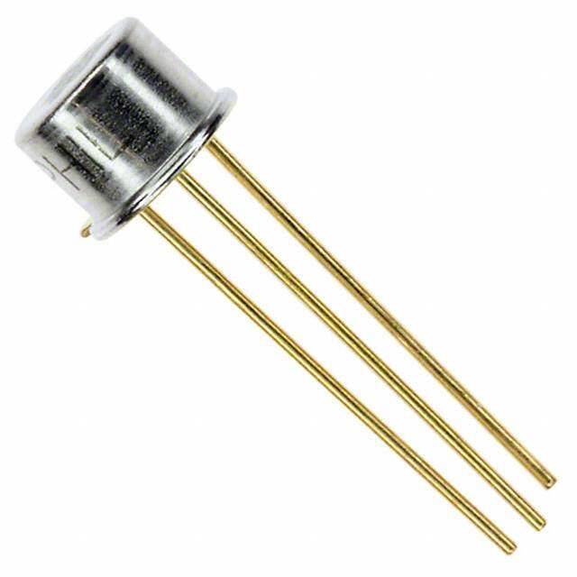
| 描述 | IC SENSOR THERMOPILE 8DSBGA板上安装温度传感器 Infrared Thermopile Sensor |
| 产品分类 | 温度传感器,变送器温度传感器 |
| 品牌 | Texas Instruments |
| 产品手册 | |
| 产品图片 |
|
| rohs | 符合RoHS无铅 / 符合限制有害物质指令(RoHS)规范要求 |
| 产品系列 | 板上安装温度传感器,Texas Instruments TMP006AIYZFR- |
| 数据手册 | |
| 产品型号 | TMP006AIYZFR |
| 产品培训模块 | http://www.digikey.cn/PTM/IndividualPTM.page?site=cn&lang=zhs&ptm=25850 |
| 产品种类 | 板上安装温度传感器 |
| 供应商器件封装 | 8-DSBGA |
| 其它名称 | 296-28819-2 |
| 制造商产品页 | http://www.ti.com/general/docs/suppproductinfo.tsp?distId=10&orderablePartNumber=TMP006AIYZFR |
| 包装 | 带卷 (TR) |
| 参考设计库 | http://www.digikey.com/rdl/4294959886/4294959871/66 |
| 商标 | Texas Instruments |
| 安装风格 | SMD/SMT |
| 封装 | Reel |
| 封装/外壳 | 8-UFBGA,DSBGA |
| 封装/箱体 | DSBGA-8 |
| 工厂包装数量 | 3000 |
| 感应温度 | -40°C ~ 125°C |
| 数字输出-位数 | 16 bit |
| 数字输出-总线接口 | 2-Wire, I2C, SMBus |
| 最大工作温度 | + 125 C |
| 最小工作温度 | - 55 C |
| 标准包装 | 3,000 |
| 电压-电源 | 2.2 V ~ 5.5 V |
| 电源电压-最大 | 7 V |
| 电源电流 | 10 mA |
| 精度 | ±1.5°C(最大) |
| 系列 | TMP006 |
| 设备功能 | Infrared Sensor |
| 输出类型 | 2 线串行, I²C/SMBUS |
| 配置 | Remote |


- 商务部:美国ITC正式对集成电路等产品启动337调查
- 曝三星4nm工艺存在良率问题 高通将骁龙8 Gen1或转产台积电
- 太阳诱电将投资9.5亿元在常州建新厂生产MLCC 预计2023年完工
- 英特尔发布欧洲新工厂建设计划 深化IDM 2.0 战略
- 台积电先进制程称霸业界 有大客户加持明年业绩稳了
- 达到5530亿美元!SIA预计今年全球半导体销售额将创下新高
- 英特尔拟将自动驾驶子公司Mobileye上市 估值或超500亿美元
- 三星加码芯片和SET,合并消费电子和移动部门,撤换高东真等 CEO
- 三星电子宣布重大人事变动 还合并消费电子和移动部门
- 海关总署:前11个月进口集成电路产品价值2.52万亿元 增长14.8%


PDF Datasheet 数据手册内容提取
Product Sample & Technical Tools & Support & Folder Buy Documents Software Community TMP006,TMP006B SBOS518E–MAY2011–REVISEDAPRIL2015 TMP006/B Infrared Thermopile Sensor in Chip-Scale Package 1 Features 3 Description • IntegratedMEMsThermopileforNoncontact The TMP006 and TMP006B are fully integrated 1 MEMs thermopile sensors that measure the TemperatureSensing temperatureofanobjectwithouthavingtobeindirect • LocalTemperatureSensorforColdJunction contact. The thermopile absorbs passive infrared Reference energy from an object at wavelengths between 4 um – ±1°C(max)from0°Cto60°C to16umwithintheend-userdefinedfieldofview. – ±1.5°C(max)from –40°Cto+125°C The corresponding change in voltage across the • Two-WireSerialInterfaceOptions: thermopile is digitized and reported with the on-chip die thermal sensor measurement through an I2C- and – I2CandSMBusCompatible SMBus-compatible interface. With this data, the – TMP006at3.3V target object temperature can be calculated by an – TMP006Bat1.8V externalprocessor. – EightProgrammableAddresses The TMP007 is an enhanced version of the TMP006 • LowPower or TMP006B. The TMP007 combines all the features of the TMP006 and TMP006B with an additional math – Supply:2.2Vto5.5V engine to perform all of the equations on chip, – ActiveCurrent:240 μA(typ) allowing the target object temperature to be read – 1-µAshutdown(max) directly from the device. The TMP007 also provides built-in nonvolatile memory for storing calibration • CompactPackage coefficients. – 1.6-mm ×1.6-mm × 0.625-mmDSBGA The Infrared thermopile sensor is specified to operate 2 Applications from –40°C to +125°C. It is possible to measure an object temperature beyond the device operating • NoncontactTemperatureSensing range as long as the device itself does not exceed – CaseTemperature theoperatingtemperaturerange(–40°Cto+125°C). – LaserPrinters DeviceInformation(1) – PowerRelays PARTNUMBER PACKAGE BODYSIZE(NOM) – HealthandBeauty TMP006 – HVACComfortOptimization DSBGA(8) 1.60mm×1.60mm TMP006B • GasConcentration (1) Forallavailablepackages,seethepackageoptionaddendum • FlameDetection attheendofthedatasheet. SimplifiedSchematic V+ + DRDY Thot 16-Bit ADR0 Thot Tcold Gain '6 CDoignittraoll TInwteor-fWaciree ADR1 Thot ADC SCL Thot Sensor SDA Amplifier IR Thermopile Die Voltage Sensor Temperature Reference TMP006 TMP006B AGND DGND 1 An IMPORTANT NOTICE at the end of this data sheet addresses availability, warranty, changes, use in safety-critical applications, intellectualpropertymattersandotherimportantdisclaimers.PRODUCTIONDATA.
TMP006,TMP006B SBOS518E–MAY2011–REVISEDAPRIL2015 www.ti.com Table of Contents 1 Features.................................................................. 1 8.5 RegisterMaps.........................................................19 2 Applications........................................................... 1 9 ApplicationandImplementation........................ 21 3 Description............................................................. 1 9.1 ApplicationInformation............................................21 4 RevisionHistory..................................................... 2 9.2 TypicalApplication .................................................21 9.3 SystemExamples...................................................24 5 DeviceComparisonTable..................................... 4 10 Power-SupplyRecommendations..................... 26 6 PinConfigurationandFunctions......................... 4 11 Layout................................................................... 27 7 Specifications......................................................... 5 11.1 LayoutGuidelines.................................................27 7.1 AbsoluteMaximumRatings.....................................5 11.2 LayoutExamples...................................................28 7.2 ESDRatings..............................................................5 12 DeviceandDocumentationSupport................. 31 7.3 RecommendedOperatingConditions.......................5 7.4 ThermalInformation..................................................5 12.1 DeviceSupport ....................................................31 7.5 ElectricalCharacteristics..........................................6 12.2 DocumentationSupport........................................31 7.6 TypicalCharacteristics..............................................7 12.3 RelatedLinks........................................................31 12.4 Trademarks...........................................................31 8 DetailedDescription.............................................. 8 12.5 ElectrostaticDischargeCaution............................31 8.1 Overview...................................................................8 12.6 Glossary................................................................31 8.2 FunctionalBlockDiagram.........................................8 13 Mechanical,Packaging,andOrderable 8.3 FeatureDescription...................................................8 Information........................................................... 32 8.4 DeviceFunctionalModes........................................19 4 Revision History NOTE:Pagenumbersforpreviousrevisionsmaydifferfrompagenumbersinthecurrentversion. ChangesfromRevisionD(November2014)toRevisionE Page • ChangedFeature,Applications,andDescriptionsections .................................................................................................... 1 • Changedthermopilesensorportionofsimplifiedschematic.................................................................................................. 1 • ChangedoperatingrangeminimumvalueinAbsoluteMaximumRatingsfrom–55°Cto–40°C.......................................... 5 • ChangedHandlingRatingstoESDRatingsandmovedstoragetemperaturetoAbsoluteMaximumRatings.....................5 • ChangedFigure3 .................................................................................................................................................................. 7 • Changedthermopilesensorportionoffunctionalblockdiagram........................................................................................... 8 • Deletedtextattheendof2ndparagraphinFieldofViewandAngularResponsesection................................................ 10 • AddedFigure8..................................................................................................................................................................... 10 • ChangedT toT inTemperatureFormatsection ........................................................................................................ 15 REG DIE ChangesfromRevisionC(December2012)toRevisionD Page • ChangedallinstancesofWCSPtoDSBGAthroughoutdatasheet...................................................................................... 1 • Changeddocumentformattolatestdatasheetstandards.................................................................................................... 1 • AddedDeviceComparison,HandlingRating,andRecommendedOperatingConditionstables,andFeature Description,DeviceFunctionalModes,RegisterMaps,ApplicationandImplementation,PowerSupply Recommendations,Layout,DeviceandDocumentationSupport,andMechanical,Packaging,andOrderable Informationsections................................................................................................................................................................ 1 • ChangedtextinfirstparagraphofDescriptionsection ......................................................................................................... 1 • Changedallinstancesof"localtemperature"to"dietemperature"throughoutdatasheet .................................................. 1 • Movedhistogramfrompage1toTypicalCharacteristicssection.......................................................................................... 1 • AddedSimplifiedSchematictitletofront-pagefigure............................................................................................................ 1 • Changedsimplifiedschematic................................................................................................................................................ 1 • DeletedPackageInformationtable ....................................................................................................................................... 4 • ChangedallT toT throughoutdatasheet.................................................................................................................. 6 Object OBJ • Changedx-andy-axislabelsinFigure1............................................................................................................................... 7 2 SubmitDocumentationFeedback Copyright©2011–2015,TexasInstrumentsIncorporated ProductFolderLinks:TMP006 TMP006B
TMP006,TMP006B www.ti.com SBOS518E–MAY2011–REVISEDAPRIL2015 • ChangedtextrelatedtoobjecttemperaturemeasurementinfirstparagraphofOverviewsection....................................... 8 • ChangedTable3.................................................................................................................................................................. 15 • ChangedallV toV throughoutdatasheet......................................................................................................... 19 OBJECT SENSOR • DeletedPointerRegistersection.......................................................................................................................................... 19 • ChangedSensorVoltageRegisternametoSensorVoltageResultRegister .................................................................... 19 • ChangedT toT throughoutdatasheet ................................................................................................................. 19 AMBIENT DIE ChangesfromRevisionB(February2012)toRevisionC Page • AddedTMP006Bdevicetodatasheet................................................................................................................................... 1 • ChangedPackageInformationtabletoincludenewTMP006BdevicewiththeTMP006,andshowthedifferent voltageforthetwodevices..................................................................................................................................................... 4 ChangesfromRevisionA(July2011)toRevisionB Page • ChangedOutputError,CalculateobjecttemperatureparametertestconditionsinElectricalCharacteristicstable.............6 • ChangeddescriptionofdeviceIDto0067hinManufacturerandDeviceIDRegisterssection........................................... 20 • ChangedFFh,ResetvaluebitsD2,D1,andD0valuesinFigure18.................................................................................. 20 • ChangedFigure23 .............................................................................................................................................................. 28 • ChangedFigure24............................................................................................................................................................... 29 • ChangedFigure25............................................................................................................................................................... 30 ChangesfromOriginal(May,2011)toRevisionA Page • Addedspecificationsforambienttemperaturesensorparameterover0°Cto+60°C........................................................... 6 • RevisedTable4.................................................................................................................................................................... 16 Copyright©2011–2015,TexasInstrumentsIncorporated SubmitDocumentationFeedback 3 ProductFolderLinks:TMP006 TMP006B
TMP006,TMP006B SBOS518E–MAY2011–REVISEDAPRIL2015 www.ti.com 5 Device Comparison Table TWO-WIRE PRODUCT INTERFACEVOLTAGE TMP006 3.3V TMP006B 1.8V 6 Pin Configuration and Functions YZFPackage 8-PinDSBGA (TopView,NottoScale) A A1 A2 A3 s w B B1 Sensor B3 o R C C1 C2 C3 1 2 3 Columns PinFunctions PIN I/O DESCRIPTION NAME NO. ADR0 C1 Input Addressselectpin ADR1 B1 Input Addressselectpin AGND A2 Power Analogground DGND A1 Power Digitalground DRDY C2 Output Dataready,activelow,open-drain;requiresapullupresistortoV+. SCL B3 Input Serialclocklinefortwo-wireinterface,open-drain;requiresapullupresistortoV+. SDA C3 Input/output Serialdatalinefortwo-wireinterface,open-drain;requiresapullupresistortoV+. V+ A3 Power Positivesupply(2.2Vto5.5V) 4 SubmitDocumentationFeedback Copyright©2011–2015,TexasInstrumentsIncorporated ProductFolderLinks:TMP006 TMP006B
TMP006,TMP006B www.ti.com SBOS518E–MAY2011–REVISEDAPRIL2015 7 Specifications 7.1 Absolute Maximum Ratings overoperatingfree-airtemperaturerange(unlessotherwisenoted)(1) MIN MAX UNIT Supplyvoltage,V V+pin 7 V S ADR1pins –0.5 V +0.5 V S Inputvoltage SDA,SCL,DRDY,ADR0pins –0.5 +7 V Inputcurrent 10 mA Operatingrange –40 +125 °C Temperature Junctiontemperature,T +150 °C Jmax Storagerange,T –65 +150 °C stg (1) StressesbeyondthoselistedunderAbsoluteMaximumRatingsmaycausepermanentdamagetothedevice.Thesearestressratings only,whichdonotimplyfunctionaloperationofthedeviceattheseoranyotherconditionsbeyondthoseindicatedunderRecommended OperatingConditions.Exposuretoabsolute-maximum-ratedconditionsforextendedperiodsmayaffectdevicereliability. 7.2 ESD Ratings VALUE UNIT Human-bodymodel(HBM),perANSI/ESDA/JEDECJS-001(1) ±2000 V Electrostatic Charged-devicemodel(CDM),perJEDECspecificationJESD22-C101(2) ±500 V (ESD) discharge Machinemodel ±200 (1) JEDECdocumentJEP155statesthat500-VHBMallowssafemanufacturingwithastandardESDcontrolprocess. (2) JEDECdocumentJEP157statesthat250-VCDMallowssafemanufacturingwithastandardESDcontrolprocess. 7.3 Recommended Operating Conditions overoperatingfree-airtemperaturerange(unlessotherwisenoted) MIN NOM MAX UNIT Supplyvoltage,V 2.5 3.3 5.5 V S Operatingtemperaturerange –40 +125 °C Dietemperature,T 125 °C DIE Objecttemperature,T Seenote (1) °C OBJ (1) Objecttemperatureisapplicationdependent. 7.4 Thermal Information TMP006 TMP006B THERMALMETRIC(1) UNIT YZF(DSBGA) 8PINS R Junction-to-ambientthermalresistance 123.8 θJA R Junction-to-case(top)thermalresistance 69 θJC(top) R Junction-to-boardthermalresistance 103 θJB °C/W ψ Junction-to-topcharacterizationparameter 4.7 JT ψ Junction-to-boardcharacterizationparameter 55 JB R Junction-to-case(bottom)thermalresistance N/A θJC(bot) (1) Formoreinformationabouttraditionalandnewthermalmetrics,seetheICPackageThermalMetricsapplicationreport,SPRA953. Copyright©2011–2015,TexasInstrumentsIncorporated SubmitDocumentationFeedback 5 ProductFolderLinks:TMP006 TMP006B
TMP006,TMP006B SBOS518E–MAY2011–REVISEDAPRIL2015 www.ti.com 7.5 Electrical Characteristics AtT =+25°C,V+=3.3V,andconversiontime=1second,unlessotherwisespecified. DIE PARAMETER TESTCONDITIONS MIN TYP MAX UNIT OUTPUTERROR TDIE=0°Cto+60°C,V+=2.2Vto5.5V ±0.5 ±1 °C Dietemperaturesensor TDIE=–40°Cto+125°C,V+=2.2Vto5.5V ±0.5 ±1.5 °C PSRR Power-supplyrejectionratio 0.1 °C/V Calculateobjecttemperature(1) TDIE=+20°Cto+60°C, ±1 ±3 °C TOBJ–TDIE=–10°Cto+30°C Fieldofview 50%responsivity 90 Degrees TEMPERATUREMEASUREMENT CR2=0,CR1=0,CR0=0 0.25 Seconds CR2=0,CR1=0,CR0=1 0.5 Seconds Conversiontime CR2=0,CR1=1,CR0=0 1 Seconds CR2=0,CR1=1,CR0=1 2 Seconds CR2=1,CR1=0,CR0=0 4 Seconds Dietemperaturesensor 0.03125 °C Resolution Thermopilesensorresolution 156.25 nV SMBusCOMPATIBLEINTERFACE TMP006only 2.1 V VIH Logicinputhighvoltage(SCL,SDA) TMP006Bonly 1.4 V TMP006only 0.8 V VIL Logicinputlowvoltage(SCL,SDA) TMP006Bonly 0.4 V Hysteresis 100 mV VOL Outputlowvoltage(SDA) IOUT=6mA 0.15 0.4 V Outputlowsinkcurrent(SDA) 6 mA Logicinputcurrent Forcedto0.4V –1 +1 µA Inputcapacitance(SCL,SDA,A0,A1) 3 pF Clockfrequency 0.001 3.4 MHz Interfacetimeout 25 30 35 ms DIGITALOUTPUTS VOL Outputlowvoltage(DRDY) IOUT=4mA 0.15 0.4 V IOH High-leveloutputleakagecurrent VOUT=VDD 0.1 1 µA Outputlowsinkcurrent(DRDY) Forcedto0.4V 4 mA POWERSUPPLY VS Specifiedvoltagerange TDIE=–40°Cto+125°C 2.2 5.5 V POR Power-onreset TDIE=–40°Cto+125°C 1.6 V Continuousconversion;seeTable7 240 325 µA Serialbusinactive,shutdownmode,TMP006 0.5 1.0 µA only IQ Quiescentcurrent Serialbusinactive,shutdownmode,TMP006B 1.5 5.0 µA only Serialbusactive,fS=400kHz, 90 µA shutdownmode (1) Thisparameteristestedinafully-settledsetupwithnotransients,infrontofanidealblackbody,withspecifiedlayoutconstraints,and aftersystemcalibration. 6 SubmitDocumentationFeedback Copyright©2011–2015,TexasInstrumentsIncorporated ProductFolderLinks:TMP006 TMP006B
TMP006,TMP006B www.ti.com SBOS518E–MAY2011–REVISEDAPRIL2015 7.6 Typical Characteristics AtT =+25°CandV =3.3V,unlessotherwisenoted. DIE S 3 4 2.5 2.2 V 3.3 V 3 2 5.5 V 1.5 2 °Error (C) 0.150 °Error (C) 10 TDIE -0-.51 TOBJ -1 -1.5 -2 -2 -3 TDIE=20°C -2.5 T =40°C DIE -3 -4 -40 -25 -10 5 20 35 50 65 80 95 110 125 -20 -10 0 10 20 30 40 T (°C) T -T (°C) DIE OBJ DIE Figure1.TypicalDieTemperatureError Figure2.TypicalObjectTemperatureError 110 20 100 90 15 %) 80 -3s +3s sivity ( 70 ount 10 on 60 C sp Field of View e 50 R 5 40 30 20 0 ±90 ±75 ±60 ±45 ±30 ±15 0 15 30 45 60 75 90 -3 -2 -1 0 1 2 3 Angle (ƒ) C001 TOBJError (°C) T =20°C,T =20°C, OBJ DIE validfor120°FOVandobjectemissivity=0.94 Figure3.ResponsivityvsAngle Figure4.Noise-Limited,Object-TemperatureAccuracy Copyright©2011–2015,TexasInstrumentsIncorporated SubmitDocumentationFeedback 7 ProductFolderLinks:TMP006 TMP006B
TMP006,TMP006B SBOS518E–MAY2011–REVISEDAPRIL2015 www.ti.com 8 Detailed Description 8.1 Overview The TMP006 and TMP006B are digital temperature sensors that are optimal for thermal management and thermal protection applications where remote noncontact sensing is desired. The TMP006 and TMP006B use a two-wire interface (I2C and SMBus compatible), and are specified over the die temperature range of –40°C to +125°C. The TMP006 and TMP006B measure object temperatures over a range limited only by the maximum sensor voltage (5.12 mV). The TMP006 and TMP006B contain registers for holding configuration information, temperature measurement results, and sensor voltage measurement. Die temperature and sensor voltage measurementsareusedtocalculatetheobjecttemperature. The TMP006 and TMP006B provide both die temperature and thermopile sensor voltage outputs in a small DSBGA chip-scale package. The die temperature sensor in both the TMP006 and TMP006B is integrated on- chip; the thermal path runs through the DSBGA solder balls. The low thermal resistance of the solder balls providesthethermalpathtomaintainthechipatthetemperatureofthedieenvironment. The top side of the DSBGA package must face the object that is being measured with an unobstructed view in order to accurately measure the temperature. Refer to the user guide TMP006 Layout and Assembly Guidelines (SBOU108)formoredetails. 8.2 Functional Block Diagram V+ + DRDY Thot 16-Bit ADR0 Thot Tcold Gain '6 CDoignittraoll TInwteor-fWaciree ADR1 Thot ADC SCL Thot Sensor SDA Amplifier IR Thermopile Die Voltage Sensor Temperature Reference TMP006 TMP006B AGND DGND 8.3 Feature Description The TMP006 and TMP006B sense the IR radiation emitted by all objects. The spectrum of the radiation depends onlyonthetemperatureandisgivenbyPlanck’slaw,asshowninEquation1: æ ö 2hc2 ç 1 ÷ B (T,l)= ç ÷watts/cm2 /mm l l5 ç hc ÷ ç ÷ èelkBT -1ø where • h=Planck’sconstant • c=speedoflight • k =Boltzmann’sconstant B • λ=wavelengthinmicrons (1) 8 SubmitDocumentationFeedback Copyright©2011–2015,TexasInstrumentsIncorporated ProductFolderLinks:TMP006 TMP006B
TMP006,TMP006B www.ti.com SBOS518E–MAY2011–REVISEDAPRIL2015 Feature Description (continued) The intensity of radiation from the object is determined by the emisivity (ε), a material-dependent property that scales the spectral response so that 0 < ε < 1. For an ideal black body, the radiation is at a maximum for a given temperature and ε = 1. The temperature is measured on the kelvin scale where 0 K is absolute zero, or –273.15°C. Room temperature (25°C) is approximately 298.13 K. The emission spectra for objects at or near room temperature are shown in Figure 5. For these temperatures, the majority of the radiation emitted is in the wavelengthrangeof3µmto20 µm. 0.025 m) 445000 KK µ 2cm/ 0.020 335000 KK W/ 250 K e ( nc 0.015 xita 4 µm 16 µm E nt 0.010 a di a R al 0.005 ctr e p S 0.000 0 5 10 15 20 Wavelength (µm) C019 Figure5. BlackBodyEmissionSpectrumandResponse 8.3.1 SpectralResponsivity The TMP006 and TMP006B are optimized to sense IR radiation emitted by objects from approximately 250 K (–23°C) to 400 K (127°C), with maximum sensitivity from approximately 4 µm to 16 µm. The relative spectral responseoftheTMP006andTMP006BisshowninFigure6. 1.2 1.0 e ns0.8 o p s e R0.6 e v elati0.4 R 0.2 0.0 4.0 8.0 12.0 16.0 Wavelength (µm) C005 Figure6. RelativeSpectralResponsevsWavelength Copyright©2011–2015,TexasInstrumentsIncorporated SubmitDocumentationFeedback 9 ProductFolderLinks:TMP006 TMP006B
TMP006,TMP006B SBOS518E–MAY2011–REVISEDAPRIL2015 www.ti.com Feature Description (continued) 8.3.2 FieldofViewandAngularResponse The TMP006 and TMP006B sense all radiation within a defined field of view (FOV). The FOV (or full-angle of θ) is defined as 2Φ. These devices contain no optical elements, and thus sense all radiation within the hemisphere to the front of the device. Figure 3 shows the angular dependence of the sensor response and the relative power foracircularobjectthatsubtendsahalfangleofphi(Φ).Figure7 definestheangle Φ intermsofobjectdiameter and distance. Figure 7 assumes that the object is well approximated as a plane that is perpendicular to the sensoraxis. Sensor - d Object D Figure7. FOVGeometryDefinition In this case, the maximum contribution is from the portion of the object directly in front of the TMP006 or TMP006B (Φ = 0); with the sensitivity per solid angle, dR/dΦ decreases as Φ increases. Approximately 50% of theenergysensedbytheTMP006andTMP006BiswithinaFOV(θ)=90°. This discussion is for illustrative purposes only; in practice the angular response (dR/dΦ) of the TMP006 and TMP006B to the object is affected by the object orientation, the number of objects, and the precise placement relativetotheTMP006orTMP006B.Figure8 showsthethermopilesensordimensions. 1.6 mm TMP006 0.165 mm 0.165 mm Sensor 0.33 mm 1.6 mm 0.33 mm NOTE:Thermopilesensoriscenteredinthedevice. Figure8. ThermopileSensorDimensions 10 SubmitDocumentationFeedback Copyright©2011–2015,TexasInstrumentsIncorporated ProductFolderLinks:TMP006 TMP006B
TMP006,TMP006B www.ti.com SBOS518E–MAY2011–REVISEDAPRIL2015 Feature Description (continued) 8.3.3 ThermopilePrinciplesandOperation The TMP006 and TMP006B sense radiation by absorbing the radiation on a hot junction. The thermopile then generates a voltage proportional to the temperature difference between the hot junction, T , and the cold hot junction,T . cold Thermopile + E ß T 4 HOT DIE T hot Thot Tcold T hot EOBJ ß TOBJ 4 Thot Heat Absorbor Cold Junction Figure9. PrincipleofThermopileOperation The cold junction is thermally grounded to the die, and is effectively T , the die temperature. In thermal DIE equilibrium, the hot junction is determined by the object temperature, T . The energy emitted by the object, OBJ E , minus the energy radiated by the die, E , determines the temperature of the hot junction. The output OBJ DIE voltage,V ,isthereforedeterminedbytherelationshipshowninEquation2: OUT V = V =C´(T -T )µ(T 4-T 4) OUT SENSOR HOT COLD OBJ DIE where • Cisaconstantdependingonthedesignofthesensingelement. (2) Note that the sensor voltage is related to both the object temperature and the die temperature. A fundamental characteristic of all thermopiles is that they measure temperature differentials, not absolute temperatures. The TMP006 and TMP006B contain a highly-accurate, internal temperature sensing element to measure T . DIE Estimate T by using V and T . For each 250-ms conversion cycle, the TMP006 and TMP006B OBJ SENSOR DIE measureavalueforV andforT ,whicharethenplacedintheirrespectiveregisters. SENSOR DIE Foreachconversioncycle,thedevicegeneratesananalog-to-digitalconverter(ADC)valueforT andV . DIE SENSOR Bits CR2 to CR0 determine the number of T and sensor ADC results to average before they are loaded into DIE therespectiveregistersforreadout. After power-on reset (POR), the TMP006 and TMP006B start in four conversions per second (CR[2:0] = 010). In general, for a mode with N conversions, the local temperature, T , result is updated at the end of the Nth ADC DIE conversionwiththevalueshowninEquation3: 1 N T = å Local Temp Conversion DIE X N X=1 (3) Similarly,thesensorvoltageresultisupdatedattheendofthe NthsensorADCconversionwiththevalueshown inEquation4: 1 N V = å SensorConversion SENSOR N X X=1 (4) The total conversion time and averages per conversion can be optimized to select the best combination of update rate versus noise for an application. Additionally, low-power conversion mode is available. In CR settings 101,110,and111,thedeviceinsertsastandbytimebeforethebeginningofthenextconversionorconversions. ThemethodandrequirementsforestimatingT aredescribedinthenextsection. OBJ Copyright©2011–2015,TexasInstrumentsIncorporated SubmitDocumentationFeedback 11 ProductFolderLinks:TMP006 TMP006B
TMP006,TMP006B SBOS518E–MAY2011–REVISEDAPRIL2015 www.ti.com Feature Description (continued) 8.3.4 ObjectTemperatureCalculation The TMP006 and TMP006B generate a sensor voltage, V , in register 00h that is representative of the Sensor energy radiated by the object. In an ideal situation, the Stefan-Boltzman law relates the energy radiated by an objecttoitstemperaturebytherelationshipshowninEquation5: Energy =esT4 Rad OBJ where • σ=Stefan-Boltzmanconstant=5.7×10⁻¹²W/cm2/K4 • ε=Emissivity,0<ε<1,anobjectdependentfactor,ε=1foraperfectblackbody (5) A similar relationship holds for the sensing element itself that radiates heat at a rate determined by T . The net DIE energy absorbed by the sensor is then given by the energy absorbed from the object minus the energy radiated bythesensor,asshowninEquation6: V µE -E =es(T4 -T4 ) SENSOR ABSORBED RADIATED OBJ DIE (6) Inanidealsituation,thesensorvoltagerelatestoobjecttemperatureasshowninEquation7: V T = 4 T4 + SENSOR OBJ DIE es (7) 4 æƒ{V }ö T = T4 +ç OBJ ÷ OBJ DIE ç S ÷ è ø where • Sisasystem-dependentparameterincorporatingtheobjectemissivity(ε),FOV,andsensorcharacteristics. TheparametersS0,A1,andA2areusedindeterminingS. • f(V )isafunctionthatcompensatesforheatflowotherthanradiation,suchasconvectionandconduction, OBJ fromnearbyobjects.TheparametersB0,B1,andB2areusedtotunethisfunctiontoaparticularsystemand environment. (8) ThecoefficientsaffectobjecttemperaturemeasurementasdescribedinTable1. Table1.CalibrationCoefficientDefinitions COEFFICIENT PURPOSE CALIBRATION COMMENT S0 FOVandemissivityofobject Applicationandobject Defaultvaluesbasedonblackbodywithε=0.95,and dependent 110°FOV A1,A2 Deviceproperties Factoryset Defaultvaluesbasedontypicalsensorcharacteristics C Deviceproperties Factoryset Defaultvaluesbasedontypicalsensorcharacteristics B0,B1,B2 Correctsforenergysources Environmentdependent Calibrateinend-applicationenvironment 12 SubmitDocumentationFeedback Copyright©2011–2015,TexasInstrumentsIncorporated ProductFolderLinks:TMP006 TMP006B
TMP006,TMP006B www.ti.com SBOS518E–MAY2011–REVISEDAPRIL2015 8.3.5 Calibration The TMP006 and TMP006B default coefficients are calibrated with a black body of emissivity, ε = 0.95, and an FOV (θ) = 110°. Use these coefficients for applications where the object emissivity and geometry satisfy these conditions. For applications with different object emissivity or geometry, calibrate the TMP006 or TMP006B to accurately reflect the object temperature and system geometry. Accuracy is affected by device-to-device or object-to-objectvariation.Forthemostdemandingapplications,calibrateeachdeviceindividually. Asanoverviewthecalibrationprocedureincludes: 1. Defining the environmental variation range (die and object temperature range, supply voltage, temperature changespeed,samplingrateandsoon). 2. Making the die temperature measurements and IR sensor voltage measurements over the environmental range. 3. Generateanoptimalsetofcoefficientsbasedonthecollecteddataset. Thebesttemperatureprecisionisavailableifeverydeviceiscalibratedindividually.Alternatively,ifalltheunitsin theapplicationusethesamecoefficients,thencalibrateastatisticallysignificantnumberofdevices. Recalibrationmayberequiredunderanyorallofthefollowingconditions: 1. Boardlayoutischanged. 2. Objectorobjectsinthefieldofviewchanged. 3. Objectdistancechanged. 4. Anglebetweendevicesurfaceanddirectiontotheobjectchanged. 5. Objectandlocaltemperaturerangechangedoutsidetheenvironmentalcalibrationrange. 6. Objectandlocaltemperaturetransientssignificantlychanged. 7. Supplyvoltagechangedmorethan1V. 8. Airconvectionorconductionnearthedevice. Forfurtherinformationandmethodsforcalibration,refertouserguideSBOU142, TMP007CalibrationGuide Copyright©2011–2015,TexasInstrumentsIncorporated SubmitDocumentationFeedback 13 ProductFolderLinks:TMP006 TMP006B
TMP006,TMP006B SBOS518E–MAY2011–REVISEDAPRIL2015 www.ti.com 8.3.6 SensorVoltageFormat The TMP006 and TMP006B provide 16 bits of data in binary twos complement format. The positive full-scale inputproducesanoutputcodeof7FFFhandthenegativefull-scaleinputproducesanoutputcodeof8000h.The output clips at these codes for signals that exceed full-scale. Table 2 summarizes the ideal output codes for different input signals. Figure 10 illustrates code transitions versus input voltage. Full-scale is a 5.12-mV signal. TheLSBsizeis156.25nV. Table2.InputSignalVersusIdealOutputCode(1) SENSORSIGNAL OUTPUTCODE FS(215–1)/215(5.12mV) 7FFFh +FS/215(156.25nV) 0001h 0 0 –FS/215(–156.25nV) FFFFh –FS(–5.12mV) 8000h (1) FS=Full-scalevalue. 7FFFh 7FFEh ¼ e 0001h d o C 0000h put FFFFh ut O ¼ 8001h 8000h ¼ ¼ -FS 0 FS Sensor Voltage (AIN -AIN ) P N 215-1 215-1 -FS FS 215 215 Figure10. CodeTransitionDiagram 14 SubmitDocumentationFeedback Copyright©2011–2015,TexasInstrumentsIncorporated ProductFolderLinks:TMP006 TMP006B
TMP006,TMP006B www.ti.com SBOS518E–MAY2011–REVISEDAPRIL2015 8.3.7 TemperatureFormat The temperature register data format of the TMP006 and TMP006B is reported in a binary twos complement signedintegerformat,asTable3shows,with1LSB=1/32°C=0.03125. Table3.TemperatureDataFormat TEMPERATURE(°C) DIGITALOUTPUT(BINARY) SHIFTEDHEX 150 0100101100000000 12C0 125 0011111010000000 0FA0 100 0011001000000000 0C80 80 0010100000000000 0A00 75 0010010110000000 0960 50 0001100100000000 0640 25 0000110010000000 0320 0.03125 0000000000000100 0001 0 0000000000000000 0000 –0.03125 1111111111111100 FFFF –0.0625 1111111111111000 FFFE –25 1111001101110000 FCDC –40 1110101111111100 FAFF –55 1110010001111100 F91F Converting the integer temperature result of the TMP006 and TMP006B to physical temperature is done by right- shifting the last two LSBs followed by a divide-by-32 of T to obtain the physical temperature result in degrees DIE Celsius. T is the 14-bit signed integer contained in the corresponding register. The sign of the temperature is DIE thesameasthesignoftheintegerreadfromtheTMP006andTMP006B.Intwoscomplementnotation,theMSB is the sign bit. If the MSB is 1, the integer is negative and the absolute value can be obtained by inverting all bits and adding 1. An alternative method of calculating the absolute value of negative integers is abs(i) = i xor FFFFh +1. 8.3.8 SerialInterface The TMP006 and TMP006B initially start up with typical settings consisting of a conversion rate of one conversionpersecond(asspecifiedintheElectricalCharacteristics).Theinternalstructureofthedigitalinterface isshowninFigure11. Pointer Register Result SCL Registers I/O Control Interface Configuration SDA Registers ADR0 ADR1 DRDY Figure11. InternalStructure Copyright©2011–2015,TexasInstrumentsIncorporated SubmitDocumentationFeedback 15 ProductFolderLinks:TMP006 TMP006B
TMP006,TMP006B SBOS518E–MAY2011–REVISEDAPRIL2015 www.ti.com The TMP006 and TMP006B operate only as a slave device on the two-wire bus. Connections to either bus are made via the open-drain I/O lines, SDA, and SCL. The SDA and SCL pins feature integrated spike-suppression filters and Schmitt triggers to minimize the effects of input spikes and bus noise. The TMP006 and TMP006B support the transmission protocol for fast (1 kHz to 400 kHz) and high-speed (1 kHz to 3.4 MHz) modes. All data bytesaretransmittedMSBfirst. 8.3.8.1 SerialBusAddress To communicate with the TMP006 or TMP006B, the master must first address slave devices via a slave address byte. The slave address byte consists of seven address bits and a direction bit that indicates the intent to executeareadorwriteoperation. The TMP006 and TMP006B feature two address pins to allow up to eight devices to be addressed on a single bus. Table 4 describes the pin logic levels used to properly connect up to eight devices. The state of the ADR0 and ADR1 pins is sampled on every bus communication and should be set before any activity on the interface occurs. Table4.TMP006andTMP006BAddressPinsandSlaveAddresses ADR1 ADR0 SMBusAddress 0 0 1000000 0 1 1000001 0 SDA 1000010 0 SCL 1000011 1 0 1000100 1 1 1000101 1 SDA 1000110 1 SCL 1000111 8.3.8.2 ReadandWriteOperations AccessaparticularregisterontheTMP006andTMP006Bbywritingtheappropriatevaluetothepointerregister. The pointer value is the first byte transferred after the slave address byte with the R/W bit low. Every write operation to the TMP006 and TMP006B requires a value for the pointer (see Figure 12). When reading from the TMP006orTMP006B,thelastvaluestoredinthepointerbyawriteoperationisusedtodeterminewhichregister is read by a read operation. To change the register pointer for a read operation, a new value must be written to the pointer. This transaction is accomplished by issuing a slave address byte with the R/W bit low, followed by thepointerbyte.Noadditionaldataarerequired.ThemastercanthengenerateaSTARTconditionandsendthe slave address byte with the R/W bit high to initiate the read command. If repeated reads from the same register are desired, it is not necessary to continually send the pointer bytes because the TMP006 and TMP006B retain the pointer value until it is changed by the next write operation. Note that register bytes are sent MSB first, followedbytheLSB. 16 SubmitDocumentationFeedback Copyright©2011–2015,TexasInstrumentsIncorporated ProductFolderLinks:TMP006 TMP006B
TMP006,TMP006B www.ti.com SBOS518E–MAY2011–REVISEDAPRIL2015 8.3.8.3 Two-WireTimingDiagrams The TMP006 and TMP006B use a two-wire interface (I2C and SMBus-compatible). Figure 12 and Figure 13 illustrate the timing for the various operations on the TMP006 and TMP006B. Parameters for Figure 12 are definedinTable5.Busdefinitionsaregivenbelow. Table5.Two-WireTimingDiagramDefinitions FASTMODE HIGH-SPEEDMODE PARAMETER TESTCONDITIONS MIN MAX MIN MAX UNIT f SCLoperatingfrequency,V >1.7V 0.001 0.4 0.001 3.4 MHz SCL S f SCLoperatingfrequency,V <1.7V 0.001 0.4 0.001 2.75 MHz SCL S BusfreetimebetweenSTOPandSTART t 600 160 ns BUF condition HoldtimeafterrepeatedSTARTcondition. t Afterthisperiod,thefirstclockis 100 100 ns HDSTA generated. t RepeatedSTARTconditionsetuptime 100 100 ns SUSTA t STOPconditionsetuptime 100 100 ns SUSTO t Dataholdtime 0(1) 0(2) ns HDDAT t Datasetuptime 100 10 ns SUDAT t SCLclocklowperiod,V >1.7V 1300 160 ns LOW S t SCLclocklowperiod,V <1.7V 1300 200 ns LOW S t SCLclockhighperiod 600 60 ns HIGH t Clock/datafalltime 300 ns F t Clock/datarisetime 300 160 ns R t Clock/datarisetimeforSCLK≤100kHz 1000 ns R (1) ForcaseswithfalltimeofSCLlessthan20nsand/ortheriseorfalltimeofSDAlessthan20ns,theholdtimeshouldbegreaterthan 20ns. (2) ForcaseswithafalltimeofSCLlessthan10nsand/ortheriseorfalltimeofSDAlessthan10ns,theholdtimeshouldbegreaterthan 10ns. BusIdle:BothSDAandSCLlinesremainhigh. Start Data Transfer: A change in the state of the SDA line from high to low while the SCL line is high defines a STARTcondition.EachdatatransferisinitiatedwithaSTARTcondition. Stop Data Transfer: A change in the state of the SDA line from low to high while the SCL line is high defines a STOPcondition.EachdatatransferterminateswithaSTOPorarepeatedSTARTcondition. DataTransfer: ThenumberofdatabytestransferredbetweenaSTARTandaSTOPconditionisnotlimitedand isdeterminedbythemasterdevice.Thereceiveracknowledgesthetransferofdata. Acknowledge: Each receiving device, when addressed, is obliged to generate an Acknowledge bit. A device that acknowledges must pull down the SDA line during the Acknowledge clock pulse in such a way that the SDA lineisstablelowduringthehighperiodoftheAcknowledgeclockpulse.Setupandholdtimesmustbetakeninto account. On a master receive, data transfer termination can be signaled by the master generating a Not- Acknowledgeonthelastbytethathasbeentransmittedbytheslave. In order for the two-wire bus to operate at frequencies above 400 kHz, the master device must issue a High- speed mode (Hs-mode) master code (0000100X) as the first byte after a START condition to switch the bus to high-speed operation. The TMP006 and TMP006B do not acknowledge this byte, but switch the input filters on SDA and SCL and the output filter on SDA to operate in Hs-mode, allowing transfers at up to 3.4 MHz. After the Hs-mode master code has been issued, the master transmits a two-wire slave address to initiate a data transfer operation. The bus continues to operate in Hs-mode until a STOP condition occurs on the bus. Upon receiving theSTOPcondition,theTMP006andTMP006Bswitchtheinputandoutputfilterbacktofast-modeoperation. Copyright©2011–2015,TexasInstrumentsIncorporated SubmitDocumentationFeedback 17 ProductFolderLinks:TMP006 TMP006B
TMP006,TMP006B SBOS518E–MAY2011–REVISEDAPRIL2015 www.ti.com 1 9 1 9 ¼ SCL ¼ SDA 1 0 0 0 0 0 0(1) R/W P7 P6 P5 P4 P3 P2 P1 P0 Start By ACK By ACK By Master Device Device Frame 1Two-Wire SlaveAddress Byte Frame 2 Pointer Register Byte 1 9 1 9 SCL (Continued) SDA (Continued) D7 D6 D5 D4 D3 D2 D1 D0 D7 D6 D5 D4 D3 D2 D1 D0 ACK By ACK By Stop By Device Device Master Frame 3 MSB Frame 4 LSB (1) Slaveaddress1000000shown.SlaveaddresschangesfortheTMP006andTMP006BdependontheADR1andADR0pinconnection. SeeTable4formoredetails. Figure12. Two-WireTimingDiagramForWriteWordFormat 1 9 1 9 SCL SDA 1 0 0 0 0 0 0(1) R/W P7 P6 P5 P4 P3 P2 P1 P0 Start By ACK By ACK By Master Device Device Frame 1Two-Wire SlaveAddress Byte Frame 2 Pointer Register Byte 1 9 1 9 SCL (Continued) SDA 1 0 0 0 0 0 0(1) R/W D7 D6 D5 D4 D3 D2 D1 D0 Start By ACK By From ACK By Master Device Device Master Frame 3Two-Wire SlaveAddress Byte Frame 4 MSB 1 9 SCL SDA D7 D6 D5 D4 D3 D2 D1 D0 From NACK By Stop By Device Master(2) Master Frame 5 LSB (1) Slaveaddress1000000shown. (2) MastermustleaveSDAhightoterminateatwo-bytereadoperation. Figure13. Two-WireTimingDiagramForTwo-ByteReadFormat 18 SubmitDocumentationFeedback Copyright©2011–2015,TexasInstrumentsIncorporated ProductFolderLinks:TMP006 TMP006B
TMP006,TMP006B www.ti.com SBOS518E–MAY2011–REVISEDAPRIL2015 8.4 Device Functional Modes The TMP006 and TMP006B operate in two modes: continuous and shutdown. A software reset function is also available. Selecting the desired operating mode is done by writing to the configuration register conversion mode select bits MOD[2:0]. The duration of the analog-to-digital (A/D) conversion is determined by the conversion rate bits CR[2:0] and is listed in Table 7. Continuous mode, on the other hand, performs an A/D conversion followed byalow-powerdelayinordertoreducetheaveragepowerconsumption.Multipleoptionsfortheconversiontime and delay time are available in order to select the desired power and noise performance. Initiating power-down has an immediate effect; it aborts the current conversion and puts the device into a low-power shutdown mode. RST,orsoftwarereset,isalsoimmediateandinitializesallmemorylocationswiththerespectiveresetvalues. 8.5 Register Maps The TMP006 and TMP006B contain data registers that hold configuration information, temperature measurement results,andstatusinformation. Table6.RegisterMap POINTER (HEX) REGISTER D15 D14 D13 D12 D11 D10 D9 D8 D7 D6 D5 D4 D3 D2 D1 D0 00h Sensorvoltage V15 V14 V13 V12 V11 V10 V9 V8 V7 V6 V5 V4 V3 V2 V1 V0 01h Localtemperature T13 T12 T11 T10 T9 T8 T7 T6 T5 T4 T3 T2 T1 T0 0 0 02h Configuration RST MOD3 MOD2 MOD1 CR3 CR2 CR1 EN DRDY 0 0 0 0 0 0 0 FEh ManufacturerID ID15 ID14 ID13 ID12 ID11 ID10 ID9 ID8 ID7 ID6 ID5 ID4 ID3 ID2 ID1 ID0 FFh DeviceID ID15 ID14 ID13 ID12 ID11 ID10 ID9 ID8 ID7 ID6 ID5 ID4 ID3 ID2 ID1 ID0 8.5.1 SensorVoltageResult(V )Register(address=00h)[reset=0000000000000000] SENSOR The sensor voltage register is a 16-bit result register in binary twos complement format. One least significant bit (LSB) is 156.25 nV. The full-scale value is a ±5.12 mV signal. Data from this register (Figure 14) are used in conjunction with data from the Temperature register to calculate the object temperature. Figure 14 summarizes the Sensor Voltage register. The equation for the resultant object temperature is discussed in the TMP006 User Guide(SBOU107). Figure14. SensorVoltageResult(V )Register SENSOR 15 14 13 12 11 10 9 8 7 6 5 4 3 2 1 0 V15 V14 V13 V12 V11 V10 V9 V8 V7 V6 V5 V4 V3 V2 V1 V0 R-0h R-0h R-0h R-0h R-0h R-0h R-0h R-0h R-0h R-0h R-0h R-0h R-0h R-0h R-0h R-0h LEGEND:R/W=Read/Write;R=Readonly;-n=valueafterreset 8.5.2 Temperature(T )Register(address=01h)[reset=0000000000000000] DIE The temperature register of the TMP006 and TMP006B is configured as a 14-bit, read-only register (as shown in Figure 15) that stores the result of the most recent conversion for the die temperature, T . Following power-up DIE orasoftwarereset,theTemperatureRegisterreads0°C(0000h)untilthefirstconversioniscomplete. Figure15. Temperature(T )Register DIE 15 14 13 12 11 10 9 8 7 6 5 4 3 2 1 0 T13 T12 T11 T10 T9 T8 T7 T6 T5 T4 T3 T2 T1 T0 — — R-0h R-0h R-0h R-0h R-0h R-0h R-0h R-0h R-0h R-0h R-0h R-0h R-0h R-0h R-0h R-0h LEGEND:R/W=Read/Write;R=Readonly;-n=valueafterreset 8.5.3 ConfigurationRegister(address=02h)[reset=0111010000000000] Figure 16 describes the configuration register. This register determines the operational modes, conversion rate, DRDY control, initiates a single conversion, performs a software reset, or puts the device into shutdown mode. Thisregisterisread/write,andthepointeraddressis02h. Copyright©2011–2015,TexasInstrumentsIncorporated SubmitDocumentationFeedback 19 ProductFolderLinks:TMP006 TMP006B
TMP006,TMP006B SBOS518E–MAY2011–REVISEDAPRIL2015 www.ti.com Figure16. ConfigurationRegister 15 14 13 12 11 10 9 8 7 6 5 4 3 2 1 0 RST MOD2 MOD1 MOD0 CR2 CR1 CR0 EN DRDY — — — — — — — R/W- R/W- R/W- R/W- R/W- R/W- R/W- R/W- R/W- R/W- R/W- R/W- R/W- R/W- R/W- R/W- 0h 1h 1h 1h 0h 1h 0h 0h 0h 0h 0h 0h 0h 0h 0h 0h LEGEND:R/W=Read/Write;R=Readonly;-n=valueafterreset Bit[15] RST:Softwareresetbit 0=Normaloperation,thisbitselfclears 1=Softwarereset Bits[14:12] MOD[2:0]:Modeofoperation 000=Power-down 111=Sensoranddiecontinuousconversion(MOD) Bits[11:9] CR[2:0]:ADCconversionrate SeeTable7. Bit[8] EN:DRDYenablebit 0=DRDYpindisabled 1=DRDYpinenabled Bit[7] DRDY:Datareadybit 0=Conversioninprogress 1=Objectvoltageandambienttemperatureresultsarereadytoread.Atemperatureorsensorvoltagereadorawriteto theConfigurationRegisterisrequiredtoclearthecondition. Bits[6:0] Unused[6:0] Table7.ConversionRate TOTALNUMBEROF PEAK-PEAKNOISE CONVERSIONRATE AVERAGED AVERAGEI OFTHET RESULT Q OBJ CR2 CR1 CR0 (conversions/sec) SAMPLES (μA) (°C) 0 0 0 4 1 240 0.5 0 0 1 2 2 240 0.35 0 1 0 1 4 240 0.25(default) 0 1 1 0.5 8 240 0.18 1 0 0 0.25 16 240 0.125 8.5.4 ManufacturerandDeviceIDRegisters TheTMP006andTMP006Bhavetwoidentificationregisters:manufacturerID(addressFEh)showninFigure17, anddeviceID(addressFFh)showninFigure18.ThemanufacturerIDreads5449handthedeviceIDis0067h. 8.5.4.1 ManufacturerIDRegister(address=FEh)[reset=0101010001001001] Figure17. ManufacturerIDRegister 15 14 13 12 11 10 9 8 7 6 5 4 3 2 1 0 ID15 ID14 ID13 ID12 ID11 ID10 ID9 ID8 ID7 ID6 ID5 ID4 ID3 ID2 ID1 ID0 R-0h R-1h R-0h R-1h R-0h R-1h R-0h R-0h R-0h R-1h R-0h R-0h R-1h R-0h R-0h R-1h LEGEND:R/W=Read/Write;R=Readonly;-n=valueafterreset 8.5.4.2 DeviceIDRegister(address=FFh)[reset=0000000001100111] Figure18. DeviceIDRegister 15 14 13 12 11 10 9 8 7 6 5 4 3 2 1 0 ID15 ID14 ID13 ID12 ID11 ID10 ID9 ID8 ID7 ID6 ID5 ID4 ID3 ID2 ID1 ID0 R-0h R-0h R-0h R-0h R-0h R-0h R-0h R-0h R-0h R-1h R-1h R-0h R-0h R-1h R-1h R-1h LEGEND:R/W=Read/Write;R=Readonly;-n=valueafterreset 20 SubmitDocumentationFeedback Copyright©2011–2015,TexasInstrumentsIncorporated ProductFolderLinks:TMP006 TMP006B
TMP006,TMP006B www.ti.com SBOS518E–MAY2011–REVISEDAPRIL2015 9 Application and Implementation NOTE Information in the following applications sections is not part of the TI component specification, and TI does not warrant its accuracy or completeness. TI’s customers are responsible for determining suitability of components for their purposes. Customers should validateandtesttheirdesignimplementationtoconfirmsystemfunctionality. 9.1 Application Information The TMP006 and TMP006B are a complete IR thermopile sensor system on a chip that includes the sensing element, signal conditioner, and ADC. These devices are ideal for applications where the object cannot be placed in thermal contact with a conventional temperature sensor. Common reasons for noncontact temperature sensingare: • Distance;theobjectistoofaraway,orinaninconvenientlocationforwiredconnections. • Theobjectisinmotion. • Directcontactoftheobjectisinconvenientoruncomfortable(forexample,skin). • Theobjectisafluid(thatis,liquidorgas). • Theobjectishazardous(forexample,acidorflammable). • Theobjectisinahazardousstate(forexample,highvoltage). 9.2 Typical Application 9.2.1 Wide-RangeCalibrationExample:T =0°Cto60°C,CommonvsUnitCalibration OBJ 2.5 V to 5.5 V V+ 0.01 µF A3 10 k(cid:13) 10 k(cid:13) 10 k(cid:13) V+ B3 SCL B1 C3 Two-Wire ADR1 TMP006 SDA Controller C1 ADR0 C2 DRDY AGND DGND A2 A1 Figure19. TypicalApplicationCircuit Copyright©2011–2015,TexasInstrumentsIncorporated SubmitDocumentationFeedback 21 ProductFolderLinks:TMP006 TMP006B
TMP006,TMP006B SBOS518E–MAY2011–REVISEDAPRIL2015 www.ti.com Typical Application (continued) 9.2.1.1 DesignRequirements Forthisapplication,thesystemmustoperateovertheenvironmentdescribedinTable8. Table8.Wide-RangeParameters DESIGNPARAMETER EXAMPLEVALUE COMMENT N 32 Numberofdevicesincalibrationset MinimumT 0°C Minimumexpecteddietemperature DIE MaximumT 60°C Maximumexpecteddietemperature DIE MinimumT 0°C Minimumexpectedobjectedtemperature OBJ MaximumT 60°C Maximumexpectedobjecttemperature OBJ ε 0.95 Objectemissivity Fieldofview 110° Fieldofviewsubtendedbyobject Conversionrate 1sample/second Select a set of values for T and T to generate the calibration set. At a minimum, include the four extreme DIE OBJ pointsofthetemperaturerangesdesired.Inpractice,itisbesttoincludeanumberofintermediatepointsaswell. ThisexampleusesthevaluesshowninTable9,withanXmarkingthevalueschosenformeasurement. Table9.Wide-RangeMeasurementValues T DIE T 0°C 20°C 40°C 60°C OBJ 0°C X X X X 20°C X X X X 40°C X X X X 60°C X X X X 9.2.1.2 DetailedDesignProcedure Before attempting to calibrate the system, it is necessary to establish the stability of the system. Noise is a measure of precision, which is the random deviation from the mean of the distribution. For a Gaussian (or normal)distribution,theprecisionistypicallycharacterizedbythestandarddeviation(sensornoise), σ. 9.2.1.2.1 Wide-RangeCalibration To begin calibration, select an object temperature (T ) and a value for the die temperature (T ). With these OBJ DIE system temperatures stable, take a statistically significant number of samples of V (results shown in register Sensor 00h). Inthisexample,64samplesweretaken. To compensate for first order drift in system temperatures, it is often useful to normalize the data set. For this purpose, for each temperature set, the sensor voltage data (given in register 00h) is normalized by first finding thebestfitlineoftheformshowninEquation9: Sensor(mV)=a´SampleNo+b (9) ThenormalizeddataforeachdatasetisthencalculatedasshowninEquation10: Sensor (mV) = Sensor -(a´SampleNo+b) NORM MEAS (10) The normalized data, V , is centered on zero mean, and is first-order corrected for long-term drift. The Sensor_norm standard deviation for each data set is then calculated to estimate the sensor noise, σ. Verify that the data are limited by white noise and no other effects. For a sensor-noise-limited data set, v σ is typically < 1 μV, and SENSOR preferably < 0.5 μV after first-order correction for drift, as described previously. If this condition is not satisfied, then the calibration accuracy is limited by external system factors (for example, convection or conduction). Repeat this process for each combination of T and T for which the calibration is to be performed. The OBJ DIE normalized data are used only for evaluating the suitability of the data set for calibration, and not for the actual calibrationitself. 22 SubmitDocumentationFeedback Copyright©2011–2015,TexasInstrumentsIncorporated ProductFolderLinks:TMP006 TMP006B
TMP006,TMP006B www.ti.com SBOS518E–MAY2011–REVISEDAPRIL2015 For calibration, the mean value, <V >, is calculated for each combination of T and T , as shown in SENSOR OBJ DIE Table 10. Using the mean value minimizes error introduced by random noise. Based on the means, a set of coefficients is generated based on a user-selected optimization criteria for Equation 7. Common criteria are minimizingthemaximumerror,minimizingtheaverageerror,andsoon.Foradetaileddiscussionofoptimization methods,seeuserguideSBOU142,TMP007CalibrationGuide. Table10.MeanValues T DIE T 0°C 20°C 40°C 60°C OBJ 0°C <V > <V > <V > <V > SENSOR SENSOR SENSOR SENSOR 20°C <V > <V > <V > <V > SENSOR SENSOR SENSOR SENSOR 40°C <V > <V > <V > <V > SENSOR SENSOR SENSOR SENSOR 60°C <V > <V > <V > <V > SENSOR SENSOR SENSOR SENSOR 9.2.1.2.2 VerifyingtheCalibration The next step is to use the generated coefficients to verify the calibration, and determine the accuracy of the system. For common calibration (C) , the same coefficients are used for all devices; in unit calibration (U) the coefficients are calculated for each device. Common calibration includes device-to-device variation, and thus is less accurate, but much easier to implement. Unit calibration is more accurate, and eliminates device variation, but requires more effort to implement. The choice depends on the application requirements for accuracy versus implementationeffort. MeancalibrationerrorateachpointisdefinedasshowninEquation11: 1åN E = (T -T ) MEAN OBJ_PREDICT OBJ_ACTUAL N 1 where • T isthetemperaturebasedonthecalibrationcoefficients. OBJ_PREDICT • T istheknownobjecttemperature,measuredindependently. OBJ_ACTUAL • Nisthenumberofdevicesinthecalibrationset. (11) The mean error graph (see Figure 20) provides an efficient method of understanding how the systematic errors vary across the temperature ranges of interest. This graph also provides a means of weighing the benefits and effortsofcommonversusunitcalibrationforaparticularapplication. Note that calibration does not affect the temporal random noise observed, as shown in Figure 21. The standard deviationofthetemperatureerrorisindependentofthecalibrationiftherandomerrorisdominatedbythesensor noise and not external system factors, such as convection and conduction. For common calibration, the total standard deviation increases because of the effects of device-to-device variation. This standard deviation is calculatedintheusualway,bysubstitutingT forthemeaninthestandarddeviationformula. OBJ_PREDICT The accuracy is then defined as the mean calibration error plus the random errors from all sources. For this exampleapplication,usethecriteriashowninEquation12: Accuracy = MeanCalibrationError ±3StandardDeviations (12) Copyright©2011–2015,TexasInstrumentsIncorporated SubmitDocumentationFeedback 23 ProductFolderLinks:TMP006 TMP006B
TMP006,TMP006B SBOS518E–MAY2011–REVISEDAPRIL2015 www.ti.com 9.2.1.3 ApplicationCurves 2.5 0.25 0°C-C 0°C-C 2.0 20°C-C 20°C-C 40°C-C C) 1.5 600°C°C-U-C C) 0.20 4600°°CC--CC ƒMean Error ( 001...050 246000°°°CCC---UUU ƒ1ms Error 1 (00..1105 0246°000C°°°CCC-U---UUU T OBJ--10..05 T rOBJ0.05 -1.5 -2.0 0.00 0 10 20 30 40 50 60 70 80 0 10 20 30 40 50 60 70 80 Object Temperature (ƒC) Object Temperature (ƒC) C015 C016 Figure20.MeanCalibrationError,WideRangeOverT Figure21.NoiseinTemperatureMeasurement,Wide DIE RangeOverT DIE 9.3 System Examples 9.3.1 UseofNEP,NETD,andResponsivityinEstimatingSystemPerformance It is often necessary to estimate system performance as part of the design process. A key system parameter is temperature accuracy for a given set of parameters. Table 11 lists example parameters for estimating system performance. Table11.EstimatingSystemPerformanceParameters DESIGNPARAMETER EXAMPLEVALUE COMMENT Objectdistance 10mm Distancetoobject Objectdiameter 15mm Objectsizeandgeometry ε 0.95 Objectemissivity T 23°C Dietemperature DIE T 30°C Maximumexpectedobjecttemperature OBJ FOV 110° Fieldofviewsubtendedbyobject Responsivity(R ) 10.8V/W ResponsivityforT =25°C,θ=0° 0 DIE Responsivity(R) 9V/W Responsivityfor110°FOV Sensorrmsnoise 0.20µV RMSsensornoiseatT =25°C DIE NEP 30nW Thermalpowerequivalenttormssensornoise Conversionrate 1SPS SPS=samplespersecond ThesystemaccuracyisafunctionofT ,T ,ε,andradiationtransfer. OBJ DIE The radiation transfer factor is system dependent, and is affected by the object distance and geometry (for example, planar versus curved surfaces, or presence of lenses). For an planar object perpendicular to the detector axis (see Figure 7), the radiation transfer follows the well-known sin2(θ) result. This expression can be usedwitharadiationtransferfunctionresponsivityvalueof9V/Wtoestimatesystemperformance. Because of the angular dependence of the TMP006 and TMP006B detector response, a more accurate representationforthesameradiativetransferfunctiongeometryisshowninEquation13: 2(cid:11)1(cid:16)cos3T(cid:12)R 0 3 where • R istheresponsivityofthedetectortoapointsourceatananglenormaltothedetector(θ=0inFigure7.R 0 0 hasavalueof~10.8V/Wat25°C. (13) Theresponsivityvalueof9V/Wisbasedonasystemwitha110° FOV. 24 SubmitDocumentationFeedback Copyright©2011–2015,TexasInstrumentsIncorporated ProductFolderLinks:TMP006 TMP006B
TMP006,TMP006B www.ti.com SBOS518E–MAY2011–REVISEDAPRIL2015 Usingthedevice-specificradiationtransferexpressionandR0,thedetectorresponseisshowninEquation14: V = 2H V (cid:11)T4 (cid:16)T4 (cid:12)A (1(cid:16)cos3T)R SENSOR OBJ B OBJ DIE det 0 3 where • ε istheemissivityoftheobject(0.95). OBJ • BistheStefan-Boltzmannconstant(5.67×10⁻¹²W/cm /K4). 2 • T istheobjecttemperature(273K+30°C). OBJ • T isthedetectortemperature(273K+23°C). DIE • A isthedetectoractivearea(1.09×10⁻³cm2) det • θisthehalf-anglesubtendedbytheobjectasviewedfromthedetector. • R istheresponsivity(~10.8V/Wforthespecifiedtemperatures). (14) 0 ThevalueofcosθisshowninEquation15: 2r cosT 0.800 4r2 (cid:14)D2 where • risthedistancebetweenthedetectorandtheobject(10mm). • Disthediameteroftheobject(15mm). (15) Differentiating with respect to object temperature, a small change in temperature creates a small change in the measuredvoltagegivenbyEquation16: 'V 8H V T3 A (cid:11)1(cid:16)cos3T(cid:12)R 'T OUT 3 OBJ B OBJ det 0 OBJ (16) SubstitutingvaluesfortheparametersyieldsEquation17: (cid:29)9 'V 2.3 uT SENSOR OBJ K (17) The sensor rms noise at T = 25°C is ~0.25 µV; thus, the rms variation in temperature measurement is as DIE showninEquation18: 'T Sensorrmsnoise 0.25 (cid:29)9 |110 mK OBJ 'V 2.3 (cid:29)9(cid:18). OUT (18) The peak-to-peak noise is approximately six times the rms noise; therefore, estimate an accuracy of approximately±0.33°C. This estimate can also be made using the noise-equivalent power (NEP), noting that NEP is the ratio of noise to responsivity,asshowninEquation19: NEP 'VROUT 83HOBJVBTO3BJAdet(cid:11)1(cid:16)cos3T(cid:12)'TOBJ §¨©213nKW·¸¹'TOBJ 0 (19) Assumingthesystemissensor-noiselimited,theNEPis~30nWat25°C,asshowninEquation20: 30 nW 'T |140 mK OBJ 213 nW/K (20) Again, the peak-to-peak noise is approximately 6X the rms noise; therefore estimate an accuracy of approximately±0.42°C. The different results from these two techniques is because of estimated values used for some parameters. The purpose of these techniques is not to obtain exact answers, but rather to quickly estimate the feasibility of a system implementation based on basic system parameters. These examples are intended only as guidelines; the specificvaluesfortheparametersdependonthespecificsystemdetails. Copyright©2011–2015,TexasInstrumentsIncorporated SubmitDocumentationFeedback 25 ProductFolderLinks:TMP006 TMP006B
TMP006,TMP006B SBOS518E–MAY2011–REVISEDAPRIL2015 www.ti.com 10 Power-Supply Recommendations The TMP006 and TMP006B are designed to operate with a power supply voltage (V ) of between 2.5 V and 5.5 S V. This input supply must be well regulated. The die temperature measurement (T ) dependence on supply DIE voltage is typically 20 m°C/V for T > 0°C. The power-on reset (POR) has a nominal value of 1.9 V at T = DIE DIE 25°C. The POR increases with decreasing die temperature. Place the decoupling capacitor (0.01 µF recommended)ascloseaspossibletothedevicewithoutobstructingthefieldofview. 26 SubmitDocumentationFeedback Copyright©2011–2015,TexasInstrumentsIncorporated ProductFolderLinks:TMP006 TMP006B
TMP006,TMP006B www.ti.com SBOS518E–MAY2011–REVISEDAPRIL2015 11 Layout 11.1 Layout Guidelines The IR thermopile sensor in the TMP006 and TMP006B is as susceptible to conducted and radiant IR energy from below the sensor on the PCB as it is to the IR energy from objects in its forward-looking field of view. When the area of PCB below the TMP006 or TMP006B is at the same temperature as the die or substrate of the TMP006 or TMP006B, heat is not transferred between the IR sensor and the PCB. However, temperature changes on a closely-placed target object or other events that lead to changes in system temperature can cause the PCB temperature and the TMP006 or TMP006B temperature to drift apart from each other. This drift in temperatures can cause a heat transfer between the IR sensor and the PCB to occur. Because of the small distance between the PCB and the bottom of the sensor, this heat energy will be conducted (as opposed to radiated) through the thin layer of air between the IR sensor and the PCB below it. This heat conduction causes offsets in the IR sensor voltage readings and ultimately leads to temperature calculation errors. To prevent and minimizetheseerrors,theTMP006andTMP006Blayoutsmustaddresscriticalfactors: Thermally isolate the TMP006 and TMP006B from the rest of the PCB and any heat sources on it. Provide a stablethermalenvironmenttoreducethenoiseinthemeasurementreadings Figure 22 illustrates the concept of thermally isolating the TMP006 and TMP006B from the PCB and external heatsourcessuchasothercomponents,aircurrents,andsoon. Target Object Field of View k BOARD TMP006 IR Sensor k TMP006 Thermally Isolated k Electrically SENSOR_PCB Connected PCB Copper Ground Empty FR-4 Material Figure22. PrincipleofTMP006andTMP006BThermalIsolation Copyright©2011–2015,TexasInstrumentsIncorporated SubmitDocumentationFeedback 27 ProductFolderLinks:TMP006 TMP006B
TMP006,TMP006B SBOS518E–MAY2011–REVISEDAPRIL2015 www.ti.com 11.2 Layout Examples Formoredetailedinformation,refertoSBOU108 —TMP006LayoutandAssemblyGuidelines. Figure23. TopLayer 28 SubmitDocumentationFeedback Copyright©2011–2015,TexasInstrumentsIncorporated ProductFolderLinks:TMP006 TMP006B
TMP006,TMP006B www.ti.com SBOS518E–MAY2011–REVISEDAPRIL2015 Layout Examples (continued) Copper Fill 15mil×15mil C3 C2 C1 B3 B1 A3 A2 A1 Pad Spacing 20mil Figure24. EnlargedView Usea12-milpadand15-milsolderballsforA1,A2,A3,B1,B3,C1,C2andC3. Copyright©2011–2015,TexasInstrumentsIncorporated SubmitDocumentationFeedback 29 ProductFolderLinks:TMP006 TMP006B
TMP006,TMP006B SBOS518E–MAY2011–REVISEDAPRIL2015 www.ti.com Layout Examples (continued) Figure25. BottomLayer 30 SubmitDocumentationFeedback Copyright©2011–2015,TexasInstrumentsIncorporated ProductFolderLinks:TMP006 TMP006B
TMP006,TMP006B www.ti.com SBOS518E–MAY2011–REVISEDAPRIL2015 12 Device and Documentation Support 12.1 Device Support 12.1.1 DeviceNomenclature The device performance is characterized by the signal, responsivity, and the noise of the sensor. The sensor noise can be characterized in terms of the raw sensor voltage, or in terms of a reference system with known opticaltransferfunction. Responsivity Ameasureofthevoltagegeneratedbythethermopileasafunctionofthethermalradiation incidentonthedevice.TheresponsivityismeasuredinV/W.Typicallyincidentradiationsarein µW andsensoroutputvoltagesin µV. SensorNoise ThenoisevoltageintrinsictothesensorgiveninnV.Thisparameterisconversion-time dependent. NoiseEquivalentPower(NEP) Thesmallestthermalpowerdifferencethatthedetectorcanreliablydetect; measuredinnW.TheNEPisafunctionofthesensornoiseandtheresponsivity. NoiseEquivalentTemperatureDifference(NETD) Thesmallesttemperaturedifferencethedetectorcan reliablydetect;measuredinmilliKelvins(mK).TheNETDisafunctionofthesensornoise, responsivityandthesystemspecificopticalpath. Forcomparisonpurposes,NETDisgivenforareferencesystemwithoutalensandwithan ideal(nonabsorbing)F/1lens. 12.2 Documentation Support 12.2.1 RelatedDocumentation TMP007CalibrationGuide,SBOU142. TMP006LayoutandAssemblyGuidelines,SBOU108. 12.3 Related Links Table 12 lists quick access links. Categories include technical documents, support and community resources, toolsandsoftware,andquickaccesstosampleorbuy. Table12.RelatedLinks TECHNICAL TOOLS& SUPPORT& PARTS PRODUCTFOLDER SAMPLE&BUY DOCUMENTS SOFTWARE COMMUNITY TMP006 Clickhere Clickhere Clickhere Clickhere Clickhere TMP006B Clickhere Clickhere Clickhere Clickhere Clickhere 12.4 Trademarks Alltrademarksarethepropertyoftheirrespectiveowners. 12.5 Electrostatic Discharge Caution This integrated circuit can be damaged by ESD. Texas Instruments recommends that all integrated circuits be handled with appropriateprecautions.Failuretoobserveproperhandlingandinstallationprocedurescancausedamage. ESDdamagecanrangefromsubtleperformancedegradationtocompletedevicefailure.Precisionintegratedcircuitsmaybemore susceptibletodamagebecauseverysmallparametricchangescouldcausethedevicenottomeetitspublishedspecifications. 12.6 Glossary SLYZ022—TIGlossary. Thisglossarylistsandexplainsterms,acronyms,anddefinitions. Copyright©2011–2015,TexasInstrumentsIncorporated SubmitDocumentationFeedback 31 ProductFolderLinks:TMP006 TMP006B
TMP006,TMP006B SBOS518E–MAY2011–REVISEDAPRIL2015 www.ti.com 13 Mechanical, Packaging, and Orderable Information The following pages include mechanical, packaging, and orderable information. This information is the most current data available for the designated devices. This data is subject to change without notice and revision of thisdocument.Forbrowser-basedversionsofthisdatasheet,refertotheleft-handnavigation. 32 SubmitDocumentationFeedback Copyright©2011–2015,TexasInstrumentsIncorporated ProductFolderLinks:TMP006 TMP006B
PACKAGE OPTION ADDENDUM www.ti.com 5-Oct-2017 PACKAGING INFORMATION Orderable Device Status Package Type Package Pins Package Eco Plan Lead/Ball Finish MSL Peak Temp Op Temp (°C) Device Marking Samples (1) Drawing Qty (2) (6) (3) (4/5) HPA01108AIYZFR NRND DSBGA YZF 8 3000 Green (RoHS SNAGCU Level-2-260C-1 YEAR -40 to 125 TMP006 & no Sb/Br) TMP006AIYZFR NRND DSBGA YZF 8 3000 Green (RoHS SNAGCU Level-2-260C-1 YEAR -40 to 125 TMP006 & no Sb/Br) TMP006AIYZFT NRND DSBGA YZF 8 250 Green (RoHS SNAGCU Level-2-260C-1 YEAR -40 to 125 TMP006 & no Sb/Br) TMP006BIYZFR NRND DSBGA YZF 8 3000 Green (RoHS SNAGCU Level-2-260C-1 YEAR -40 to 125 T006B & no Sb/Br) TMP006BIYZFT NRND DSBGA YZF 8 250 Green (RoHS SNAGCU Level-2-260C-1 YEAR -40 to 125 T006B & no Sb/Br) (1) The marketing status values are defined as follows: ACTIVE: Product device recommended for new designs. LIFEBUY: TI has announced that the device will be discontinued, and a lifetime-buy period is in effect. NRND: Not recommended for new designs. Device is in production to support existing customers, but TI does not recommend using this part in a new design. PREVIEW: Device has been announced but is not in production. Samples may or may not be available. OBSOLETE: TI has discontinued the production of the device. (2) RoHS: TI defines "RoHS" to mean semiconductor products that are compliant with the current EU RoHS requirements for all 10 RoHS substances, including the requirement that RoHS substance do not exceed 0.1% by weight in homogeneous materials. Where designed to be soldered at high temperatures, "RoHS" products are suitable for use in specified lead-free processes. TI may reference these types of products as "Pb-Free". RoHS Exempt: TI defines "RoHS Exempt" to mean products that contain lead but are compliant with EU RoHS pursuant to a specific EU RoHS exemption. Green: TI defines "Green" to mean the content of Chlorine (Cl) and Bromine (Br) based flame retardants meet JS709B low halogen requirements of <=1000ppm threshold. Antimony trioxide based flame retardants must also meet the <=1000ppm threshold requirement. (3) MSL, Peak Temp. - The Moisture Sensitivity Level rating according to the JEDEC industry standard classifications, and peak solder temperature. (4) There may be additional marking, which relates to the logo, the lot trace code information, or the environmental category on the device. (5) Multiple Device Markings will be inside parentheses. Only one Device Marking contained in parentheses and separated by a "~" will appear on a device. If a line is indented then it is a continuation of the previous line and the two combined represent the entire Device Marking for that device. (6) Lead/Ball Finish - Orderable Devices may have multiple material finish options. Finish options are separated by a vertical ruled line. Lead/Ball Finish values may wrap to two lines if the finish value exceeds the maximum column width. Addendum-Page 1
PACKAGE OPTION ADDENDUM www.ti.com 5-Oct-2017 Important Information and Disclaimer:The information provided on this page represents TI's knowledge and belief as of the date that it is provided. TI bases its knowledge and belief on information provided by third parties, and makes no representation or warranty as to the accuracy of such information. Efforts are underway to better integrate information from third parties. TI has taken and continues to take reasonable steps to provide representative and accurate information but may not have conducted destructive testing or chemical analysis on incoming materials and chemicals. TI and TI suppliers consider certain information to be proprietary, and thus CAS numbers and other limited information may not be available for release. In no event shall TI's liability arising out of such information exceed the total purchase price of the TI part(s) at issue in this document sold by TI to Customer on an annual basis. Addendum-Page 2
PACKAGE MATERIALS INFORMATION www.ti.com 5-Oct-2017 TAPE AND REEL INFORMATION *Alldimensionsarenominal Device Package Package Pins SPQ Reel Reel A0 B0 K0 P1 W Pin1 Type Drawing Diameter Width (mm) (mm) (mm) (mm) (mm) Quadrant (mm) W1(mm) TMP006AIYZFR DSBGA YZF 8 3000 180.0 8.4 1.65 1.65 0.81 4.0 8.0 Q1 TMP006AIYZFT DSBGA YZF 8 250 180.0 8.4 1.65 1.65 0.81 4.0 8.0 Q1 TMP006BIYZFR DSBGA YZF 8 3000 180.0 8.4 1.65 1.65 0.81 4.0 8.0 Q1 TMP006BIYZFT DSBGA YZF 8 250 180.0 8.4 1.65 1.65 0.81 4.0 8.0 Q1 PackMaterials-Page1
PACKAGE MATERIALS INFORMATION www.ti.com 5-Oct-2017 *Alldimensionsarenominal Device PackageType PackageDrawing Pins SPQ Length(mm) Width(mm) Height(mm) TMP006AIYZFR DSBGA YZF 8 3000 182.0 182.0 20.0 TMP006AIYZFT DSBGA YZF 8 250 182.0 182.0 20.0 TMP006BIYZFR DSBGA YZF 8 3000 182.0 182.0 20.0 TMP006BIYZFT DSBGA YZF 8 250 182.0 182.0 20.0 PackMaterials-Page2
D: Max = 1.566 mm, Min =1 .506 mm E: Max = 1.566 mm, Min =1 .506 mm
IMPORTANTNOTICE TexasInstrumentsIncorporated(TI)reservestherighttomakecorrections,enhancements,improvementsandotherchangestoits semiconductorproductsandservicesperJESD46,latestissue,andtodiscontinueanyproductorserviceperJESD48,latestissue.Buyers shouldobtainthelatestrelevantinformationbeforeplacingordersandshouldverifythatsuchinformationiscurrentandcomplete. TI’spublishedtermsofsaleforsemiconductorproducts(http://www.ti.com/sc/docs/stdterms.htm)applytothesaleofpackagedintegrated circuitproductsthatTIhasqualifiedandreleasedtomarket.AdditionaltermsmayapplytotheuseorsaleofothertypesofTIproductsand services. ReproductionofsignificantportionsofTIinformationinTIdatasheetsispermissibleonlyifreproductioniswithoutalterationandis accompaniedbyallassociatedwarranties,conditions,limitations,andnotices.TIisnotresponsibleorliableforsuchreproduced documentation.Informationofthirdpartiesmaybesubjecttoadditionalrestrictions.ResaleofTIproductsorserviceswithstatements differentfromorbeyondtheparametersstatedbyTIforthatproductorservicevoidsallexpressandanyimpliedwarrantiesforthe associatedTIproductorserviceandisanunfairanddeceptivebusinesspractice.TIisnotresponsibleorliableforanysuchstatements. BuyersandotherswhoaredevelopingsystemsthatincorporateTIproducts(collectively,“Designers”)understandandagreethatDesigners remainresponsibleforusingtheirindependentanalysis,evaluationandjudgmentindesigningtheirapplicationsandthatDesignershave fullandexclusiveresponsibilitytoassurethesafetyofDesigners'applicationsandcomplianceoftheirapplications(andofallTIproducts usedinorforDesigners’applications)withallapplicableregulations,lawsandotherapplicablerequirements.Designerrepresentsthat,with respecttotheirapplications,Designerhasallthenecessaryexpertisetocreateandimplementsafeguardsthat(1)anticipatedangerous consequencesoffailures,(2)monitorfailuresandtheirconsequences,and(3)lessenthelikelihoodoffailuresthatmightcauseharmand takeappropriateactions.DesigneragreesthatpriortousingordistributinganyapplicationsthatincludeTIproducts,Designerwill thoroughlytestsuchapplicationsandthefunctionalityofsuchTIproductsasusedinsuchapplications. TI’sprovisionoftechnical,applicationorotherdesignadvice,qualitycharacterization,reliabilitydataorotherservicesorinformation, including,butnotlimitedto,referencedesignsandmaterialsrelatingtoevaluationmodules,(collectively,“TIResources”)areintendedto assistdesignerswhoaredevelopingapplicationsthatincorporateTIproducts;bydownloading,accessingorusingTIResourcesinany way,Designer(individuallyor,ifDesignerisactingonbehalfofacompany,Designer’scompany)agreestouseanyparticularTIResource solelyforthispurposeandsubjecttothetermsofthisNotice. TI’sprovisionofTIResourcesdoesnotexpandorotherwisealterTI’sapplicablepublishedwarrantiesorwarrantydisclaimersforTI products,andnoadditionalobligationsorliabilitiesarisefromTIprovidingsuchTIResources.TIreservestherighttomakecorrections, enhancements,improvementsandotherchangestoitsTIResources.TIhasnotconductedanytestingotherthanthatspecifically describedinthepublisheddocumentationforaparticularTIResource. Designerisauthorizedtouse,copyandmodifyanyindividualTIResourceonlyinconnectionwiththedevelopmentofapplicationsthat includetheTIproduct(s)identifiedinsuchTIResource.NOOTHERLICENSE,EXPRESSORIMPLIED,BYESTOPPELOROTHERWISE TOANYOTHERTIINTELLECTUALPROPERTYRIGHT,ANDNOLICENSETOANYTECHNOLOGYORINTELLECTUALPROPERTY RIGHTOFTIORANYTHIRDPARTYISGRANTEDHEREIN,includingbutnotlimitedtoanypatentright,copyright,maskworkright,or otherintellectualpropertyrightrelatingtoanycombination,machine,orprocessinwhichTIproductsorservicesareused.Information regardingorreferencingthird-partyproductsorservicesdoesnotconstitutealicensetousesuchproductsorservices,orawarrantyor endorsementthereof.UseofTIResourcesmayrequirealicensefromathirdpartyunderthepatentsorotherintellectualpropertyofthe thirdparty,oralicensefromTIunderthepatentsorotherintellectualpropertyofTI. TIRESOURCESAREPROVIDED“ASIS”ANDWITHALLFAULTS.TIDISCLAIMSALLOTHERWARRANTIESOR REPRESENTATIONS,EXPRESSORIMPLIED,REGARDINGRESOURCESORUSETHEREOF,INCLUDINGBUTNOTLIMITEDTO ACCURACYORCOMPLETENESS,TITLE,ANYEPIDEMICFAILUREWARRANTYANDANYIMPLIEDWARRANTIESOF MERCHANTABILITY,FITNESSFORAPARTICULARPURPOSE,ANDNON-INFRINGEMENTOFANYTHIRDPARTYINTELLECTUAL PROPERTYRIGHTS.TISHALLNOTBELIABLEFORANDSHALLNOTDEFENDORINDEMNIFYDESIGNERAGAINSTANYCLAIM, INCLUDINGBUTNOTLIMITEDTOANYINFRINGEMENTCLAIMTHATRELATESTOORISBASEDONANYCOMBINATIONOF PRODUCTSEVENIFDESCRIBEDINTIRESOURCESOROTHERWISE.INNOEVENTSHALLTIBELIABLEFORANYACTUAL, DIRECT,SPECIAL,COLLATERAL,INDIRECT,PUNITIVE,INCIDENTAL,CONSEQUENTIALOREXEMPLARYDAMAGESIN CONNECTIONWITHORARISINGOUTOFTIRESOURCESORUSETHEREOF,ANDREGARDLESSOFWHETHERTIHASBEEN ADVISEDOFTHEPOSSIBILITYOFSUCHDAMAGES. UnlessTIhasexplicitlydesignatedanindividualproductasmeetingtherequirementsofaparticularindustrystandard(e.g.,ISO/TS16949 andISO26262),TIisnotresponsibleforanyfailuretomeetsuchindustrystandardrequirements. WhereTIspecificallypromotesproductsasfacilitatingfunctionalsafetyorascompliantwithindustryfunctionalsafetystandards,such productsareintendedtohelpenablecustomerstodesignandcreatetheirownapplicationsthatmeetapplicablefunctionalsafetystandards andrequirements.Usingproductsinanapplicationdoesnotbyitselfestablishanysafetyfeaturesintheapplication.Designersmust ensurecompliancewithsafety-relatedrequirementsandstandardsapplicabletotheirapplications.DesignermaynotuseanyTIproductsin life-criticalmedicalequipmentunlessauthorizedofficersofthepartieshaveexecutedaspecialcontractspecificallygoverningsuchuse. Life-criticalmedicalequipmentismedicalequipmentwherefailureofsuchequipmentwouldcauseseriousbodilyinjuryordeath(e.g.,life support,pacemakers,defibrillators,heartpumps,neurostimulators,andimplantables).Suchequipmentincludes,withoutlimitation,all medicaldevicesidentifiedbytheU.S.FoodandDrugAdministrationasClassIIIdevicesandequivalentclassificationsoutsidetheU.S. TImayexpresslydesignatecertainproductsascompletingaparticularqualification(e.g.,Q100,MilitaryGrade,orEnhancedProduct). Designersagreethatithasthenecessaryexpertisetoselecttheproductwiththeappropriatequalificationdesignationfortheirapplications andthatproperproductselectionisatDesigners’ownrisk.Designersaresolelyresponsibleforcompliancewithalllegalandregulatory requirementsinconnectionwithsuchselection. DesignerwillfullyindemnifyTIanditsrepresentativesagainstanydamages,costs,losses,and/orliabilitiesarisingoutofDesigner’snon- compliancewiththetermsandprovisionsofthisNotice. MailingAddress:TexasInstruments,PostOfficeBox655303,Dallas,Texas75265 Copyright©2017,TexasInstrumentsIncorporated