ICGOO在线商城 > 传感器,变送器 > 温度传感器 - 模拟和数字输出 > LMT84DCKT
 Datasheet下载
- 型号: LMT84DCKT
- 制造商: Texas Instruments
- 库位|库存: xxxx|xxxx
- 要求:
| 数量阶梯 | 香港交货 | 国内含税 |
| +xxxx | $xxxx | ¥xxxx |
查看当月历史价格
查看今年历史价格
LMT84DCKT产品简介:
ICGOO电子元器件商城为您提供LMT84DCKT由Texas Instruments设计生产,在icgoo商城现货销售,并且可以通过原厂、代理商等渠道进行代购。 LMT84DCKT价格参考。Texas InstrumentsLMT84DCKT封装/规格:温度传感器 - 模拟和数字输出, 温度传感器 模拟,本地 -50°C ~ 150°C 5.5mV/°C SC-70-5。您可以下载LMT84DCKT参考资料、Datasheet数据手册功能说明书,资料中有LMT84DCKT 详细功能的应用电路图电压和使用方法及教程。
Texas Instruments(德州仪器)的LMT84DCKT是一款温度传感器,具有模拟和数字输出功能。该器件广泛应用于需要精确温度监测与控制的各种场景中。以下是其主要应用场景:

1. 消费电子产品:LMT84DCKT适用于智能手机、平板电脑、笔记本电脑等便携式设备。它能够实时监控设备内部温度,确保在高温环境下自动调节性能,防止过热导致的损坏或降频。

2. 工业自动化:在工厂自动化系统中,该传感器可以用于电机驱动器、PLC(可编程逻辑控制器)、变频器等设备的温度检测。通过精准的温度反馈,帮助优化生产流程并提高能效。

3. 通信基础设施:基站、路由器、交换机等通信设备需要稳定的运行环境。LMT84DCKT可用于这些设备的关键部件如电源模块、处理器等处进行温度监控,保证信号传输质量和延长使用寿命。

4. 医疗设备:对于MRI(磁共振成像)、CT扫描仪等大型医疗成像设备而言,温度控制至关重要。LMT84DCKT能提供高精度的温度测量,有助于维持设备的最佳工作状态,保障诊断结果准确性。

5. 汽车电子:现代汽车中的电池管理系统、发动机控制单元、车载信息娱乐系统等都需要可靠的温度传感解决方案。LMT84DCKT以其小巧尺寸和低功耗特性成为理想选择,在狭小空间内实现高效温控。

6. 智能家居:智能恒温器、空调控制系统等家庭自动化产品也离不开准确的温度感知。LMT84DCKT凭借其双输出模式,既可直接显示温度读数,又能与其他微控制器无缝对接,实现智能化温控管理。

总之,LMT84DCKT凭借其出色的性能表现,在众多领域发挥着重要作用,为各类应用提供了稳定可靠的温度监测手段。
| 参数 | 数值 |
| 产品目录 | |
| 描述 | IC TEMP SENSOR CLASS-AB SC-70-5板上安装温度传感器 1.5V,Multi-Gain Ana Temp Sensor |
| 产品分类 | 温度传感器,变送器温度传感器 |
| 品牌 | Texas Instruments |
| 产品手册 | http://www.ti.com/lit/gpn/lmt84 |
| 产品图片 |
|
| rohs | 符合RoHS无铅 / 符合限制有害物质指令(RoHS)规范要求 |
| 产品系列 | 板上安装温度传感器,Texas Instruments LMT84DCKT- |
| 数据手册 | |
| 产品型号 | LMT84DCKT |
| 产品培训模块 | http://www.digikey.cn/PTM/IndividualPTM.page?site=cn&lang=zhs&ptm=30170 |
| 产品种类 | 板上安装温度传感器 |
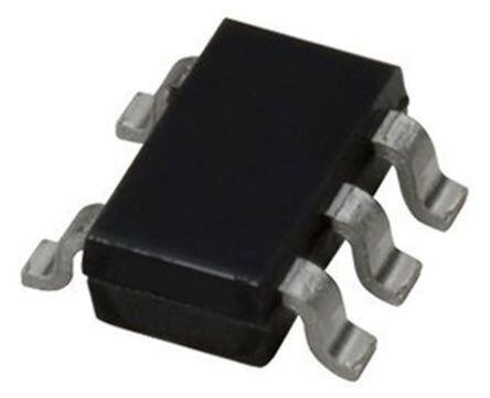
| 供应商器件封装 | SC-70-5 |
| 关闭 | No Shutdown |
| 其它名称 | 296-35727-1 |
| 准确性 | +/- 2.7 C |
| 包装 | 剪切带 (CT) |
| 商标 | Texas Instruments |
| 增益 | - 5.5 mV / C |
| 安装风格 | SMD/SMT |
| 封装 | Reel |
| 封装/外壳 | 6-TSSOP(5 引线),SC-88A,SOT-353 |
| 封装/箱体 | SC-70-5 |
| 工厂包装数量 | 250 |
| 感应温度 | -50°C ~ 150°C |
| 数字输出-总线接口 | - |
| 最大工作温度 | + 150 C |
| 最小工作温度 | - 50 C |
| 标准包装 | 1 |
| 特色产品 | http://www.digikey.cn/product-highlights/zh/lmt84-analog-temperature-sensor/52901 |
| 电压-电源 | 1.5 V ~ 5.5 V |
| 电源电压-最大 | 5.5 V |
| 电源电压-最小 | 1.5 V |
| 电源电流 | 5.4 uA |
| 精度 | ±0.6°C |
| 系列 | LMT84 |
| 设备功能 | Temperature Sensor |
| 输出电流 | 7 mA |
| 输出类型 | 推挽式 |
| 配置 | Local |


- 商务部:美国ITC正式对集成电路等产品启动337调查
- 曝三星4nm工艺存在良率问题 高通将骁龙8 Gen1或转产台积电
- 太阳诱电将投资9.5亿元在常州建新厂生产MLCC 预计2023年完工
- 英特尔发布欧洲新工厂建设计划 深化IDM 2.0 战略
- 台积电先进制程称霸业界 有大客户加持明年业绩稳了
- 达到5530亿美元!SIA预计今年全球半导体销售额将创下新高
- 英特尔拟将自动驾驶子公司Mobileye上市 估值或超500亿美元
- 三星加码芯片和SET,合并消费电子和移动部门,撤换高东真等 CEO
- 三星电子宣布重大人事变动 还合并消费电子和移动部门
- 海关总署:前11个月进口集成电路产品价值2.52万亿元 增长14.8%


PDF Datasheet 数据手册内容提取
Product Order Technical Tools & Support & Folder Now Documents Software Community LMT84 SNIS167E–MARCH2013–REVISEDOCTOBER2017 LMT84 1.5-V, SC70/TO-92/TO-92S, Analog Temperature Sensors 1 Features 3 Description • LMT84LPG(TO-92Spackage)hasaFast The LMT84 is a precision CMOS temperature sensor 1 with ±0.4°C typical accuracy (±2.7°C maximum) and ThermalTimeConstant,10-sTypical(1.2m/s a linear analog output voltage that is inversely Airflow) proportional to temperature. The 1.5-V supply voltage • VeryAccurate: ±0.4°CTypical operation, 5.4-μA quiescent current, and 0.7-ms • Low1.5-VOperation power-on time enable effective power-cycling architectures to minimize power consumption for • AverageSensorGainof-5.5mV/°C battery-powered applications such as drones and • Low5.4-µAQuiescentCurrent sensor nodes. The LMT84LPG through-hole TO-92S • WideTemperatureRange:–50°Cto150°C package fast thermal time constant supports off- • OutputisShort-CircuitProtected board time-temperature sensitive applications such as smoke and heat detectors. The accuracy over the • Push-PullOutputWith ±50-µADriveCapability wide operating range and other features make the • FootprintCompatibleWiththeIndustry-Standard LMT84anexcellentalternativetothermistors. LM20/19andLM35TemperatureSensors For devices with different average sensor gains and • Cost-EffectiveAlternativetoThermistors comparable accuracy, refer to Comparable Alternative Devices for alternative devices in the 2 Applications LMT8xfamily. • InfotainmentandCluster DeviceInformation(1) • PowertrainSystems PARTNUMBER PACKAGE BODYSIZE(NOM) • SmokeandHeatDetectors SOT(5) 2.00mmx1.25mm • Drones LMT84 TO-92(3) 4.30mmx3.50mm • Appliances TO-92S(3) 4.00mmx3.15mm (1) Forallavailablepackages,seetheorderableaddendum addendumattheendofthedatasheet. ThermalTimeConstant OutputVoltagevsTemperature 100% VDD (+1.5V to +5.5V) 90% 80% VDD E UR 70% T RA 60% LMT84 PE 50% CBP OUT M E T 40% L NA 30% FI 20% GND 10% LMT8xLPG Thermistor 0 0 20 40 60 80 100 TIME (s) Copyright © 2016, Texas Instruments Incorporated D003 *FastthermalresponseNTC 1 An IMPORTANT NOTICE at the end of this data sheet addresses availability, warranty, changes, use in safety-critical applications, intellectualpropertymattersandotherimportantdisclaimers.PRODUCTIONDATA.
LMT84 SNIS167E–MARCH2013–REVISEDOCTOBER2017 www.ti.com Table of Contents 1 Features.................................................................. 1 8.3 FeatureDescription...................................................9 2 Applications........................................................... 1 8.4 DeviceFunctionalModes........................................11 3 Description............................................................. 1 9 ApplicationandImplementation........................ 13 4 RevisionHistory..................................................... 2 9.1 ApplicationsInformation..........................................13 9.2 TypicalApplications................................................13 5 DeviceComparisonTables................................... 3 10 PowerSupplyRecommendations..................... 14 6 PinConfigurationandFunctions......................... 4 11 Layout................................................................... 15 7 Specifications......................................................... 5 11.1 LayoutGuidelines.................................................15 7.1 AbsoluteMaximumRatings......................................5 11.2 LayoutExamples...................................................15 7.2 ESDRatings..............................................................5 12 DeviceandDocumentationSupport................. 16 7.3 RecommendedOperatingConditions.......................5 7.4 ThermalInformation..................................................5 12.1 ReceivingNotificationofDocumentationUpdates16 7.5 AccuracyCharacteristics...........................................6 12.2 CommunityResources..........................................16 7.6 ElectricalCharacteristics...........................................6 12.3 Trademarks...........................................................16 7.7 TypicalCharacteristics..............................................7 12.4 ElectrostaticDischargeCaution............................16 12.5 Glossary................................................................16 8 DetailedDescription.............................................. 9 13 Mechanical,Packaging,andOrderable 8.1 Overview...................................................................9 Information........................................................... 16 8.2 FunctionalBlockDiagram.........................................9 4 Revision History NOTE:Pagenumbersforpreviousrevisionsmaydifferfrompagenumbersinthecurrentversion. ChangesfromRevisionD(June2017)toRevisionE Page • Movedtheautomotivedevicetoastandalonedatasheet(SNIS178)................................................................................... 1 • ChangedTO-92GNDpinnumberfrom:1to:3 .................................................................................................................... 4 • ChangedTO-92V pinnumberfrom:3to:1 ...................................................................................................................... 4 DD ChangesfromRevisionC(October2015)toRevisionD Page • Updateddatasheettexttothelatestdocumentationandtranslationsstandards................................................................. 1 • AddedAEC-Q100automotivequalificationbulletstoFeatures............................................................................................. 1 • AddedTimeConstantgraph................................................................................................................................................... 1 • Removeddiskdrivers,games,wirelesstransceivers,andcellphonesfromApplications..................................................... 1 • AddedLPG(TO-92S)package.............................................................................................................................................. 4 • AddedFigure10toTypicalCharacteristics............................................................................................................................ 7 ChangesfromRevisionB(May2014)toRevisionC Page • DeletedallmentionsofTO-126package .............................................................................................................................. 1 • AddedTO-92LPMpinconfigurationgraphic......................................................................................................................... 4 • ChangedHandlingRatingstoESDRatingsandmovedStorageTemperaturetoAbsoluteMaximumRatingstable...........5 • ChangedKVtoV ................................................................................................................................................................... 5 • AddedlayoutrecommendationforTO-92LPandLPMpackages....................................................................................... 15 ChangesfromRevisionA(June2013)toRevisionB Page • ChangeddatasheetflowandlayouttoconformwithnewTIstandards.Addedthefollowingsections:Application andImplementation,PowerSupplyRecommendations,Layout,DeviceandDocumentationSupport,Mechanical, Packaging,andOrderableInformation. ................................................................................................................................. 1 • AddedTO-92andTO-126packageinformationthroughoutdocument................................................................................. 1 2 SubmitDocumentationFeedback Copyright©2013–2017,TexasInstrumentsIncorporated ProductFolderLinks:LMT84
LMT84 www.ti.com SNIS167E–MARCH2013–REVISEDOCTOBER2017 • Changedfrom450°C/Wto275°C/W.NewspecificationisderivedusingTI'slatestmethodology. .................................. 5 • DeletedNote:Theinputcurrentisleakageonlyandishighestathightemperature.Itistypicallyonly0.001µA.The 1µAlimitissolelybasedonatestinglimitationanddoesnotreflecttheactualperformanceofthepart. .......................... 6 5 Device Comparison Tables Table1.AvailableDevicePackages ORDERNUMBER(1) PACKAGE PIN BODYSIZE(NOM) MOUNTINGTYPE LMT84DCK SOT(AKA(2):SC70,DCK) 5 2.00mm×1.25mm SurfaceMount LMT84LP TO-92(AKA(2):LP) 3 4.30mm×3.50mm Through-hole;straightleads LMT84LPG TO-92S(AKA(2):LPG) 3 4.00mm×3.15mm Through-hole;straightleads LMT84LPM TO-92(AKA(2):LPM) 3 4.30mm×3.50mm Through-hole;formedleads LMT84DCK-Q1 SOT(AKA(2):SC70,DCK) 5 2.00mm×1.25mm SurfaceMount (1) Forallavailablepackagesandcompleteordernumbers,seethePackageOptionaddendumattheendofthedatasheet. (2) AKA=AlsoKnownAs Table2.ComparableAlternativeDevices DEVICENAME AVERAGEOUTPUTSENSORGAIN POWERSUPPLYRANGE LMT84 –5.5mV/°C 1.5Vto5.5V LMT85 –8.2mV/°C 1.8Vto5.5V LMT86 –10.9mV/°C 2.2Vto5.5V LMT87 –13.6mV/°C 2.7Vto5.5V Copyright©2013–2017,TexasInstrumentsIncorporated SubmitDocumentationFeedback 3 ProductFolderLinks:LMT84
LMT84 SNIS167E–MARCH2013–REVISEDOCTOBER2017 www.ti.com 6 Pin Configuration and Functions LPPackage DCKPackage 3-PinTO-92 5-PinSOT(SC70) (TopView) (TopView) 1 5 GND GND 2 GND LMT84 3 4 OUT VDD LPGPackage V1 DD 3-PinTO-92S (TopView) OUT2 GND3 Scale: 4:1 1 2 3 LPMPackage 3-PinTO-92 (TopView) O1 UT GND2 VDD3 Scale: 4:1 V1 DD O2 UT G3 N D Scale: 4:1 PinFunctions PIN DESCRIPTION TYPE NAME SOT(SC70) TO-92 TO-92S EQUIVALENTCIRCUIT FUNCTION GND 1,2(1),5 3 2 Ground N/A PowerSupplyGround VDD Analog Outputsavoltagethatisinversely OUT 3 2 1 Output proportionaltotemperature GND V 4 1 3 Power N/A PositiveSupplyVoltage DD (1) Directconnectiontothebacksideofthedie 4 SubmitDocumentationFeedback Copyright©2013–2017,TexasInstrumentsIncorporated ProductFolderLinks:LMT84
LMT84 www.ti.com SNIS167E–MARCH2013–REVISEDOCTOBER2017 7 Specifications 7.1 Absolute Maximum Ratings See (1)(2) MIN MAX UNIT Supplyvoltage –0.3 6 V Voltageatoutputpin –0.3 (V +0.5) V DD Outputcurrent –7 7 mA Inputcurrentatanypin(3) –5 5 mA Maximumjunctiontemperature(T ) 150 °C JMAX StoragetemperatureT –65 150 °C stg (1) StressesbeyondthoselistedunderAbsoluteMaximumRatingsmaycausepermanentdamagetothedevice.Thesearestressratings only,whichdonotimplyfunctionaloperationofthedeviceattheseoranyotherconditionsbeyondthoseindicatedunderRecommended OperatingConditions.Exposuretoabsolute-maximum-ratedconditionsforextendedperiodsmayaffectdevicereliability. (2) SolderingprocessmustcomplywithReflowTemperatureProfilespecifications.Refertowww.ti.com/packaging. (3) Whentheinputvoltage(V)atanypinexceedspowersupplies(V <GNDorV >V),thecurrentatthatpinshouldbelimitedto5mA. I I I 7.2 ESD Ratings VALUE UNIT LMT84LPinTO-92/TO-92Spackage Electrostatic Human-bodymodel(HBM),perANSI/ESDA/JEDECJS-001(1)(2) ±2500 V V (ESD) discharge Charged-devicemodel(CDM),perJEDECspecificationJESD22-C101(3) ±1000 LMT84DCKinSC70package Electrostatic Human-bodymodel(HBM),perJESD22-A114(2) ±2500 V V (ESD) discharge Charged-devicemodel(CDM),perJEDECspecificationJESD22-C101(3) ±1000 (1) JEDECdocumentJEP155statesthat500-VHBMallowssafemanufacturingwithastandardESDcontrolprocess. (2) Thehumanbodymodelisa100-pFcapacitordischargedthrougha1.5-kΩresistorintoeachpin. (3) JEDECdocumentJEP157statesthat250-VCDMallowssafemanufacturingwithastandardESDcontrolprocess. 7.3 Recommended Operating Conditions MIN MAX UNIT T ≤T ≤T °C MIN A MAX Specifiedtemperature −50≤T ≤150 °C A Supplyvoltage(V ) 1.5 5.5 V DD 7.4 Thermal Information(1) LMT84/ LMT84LP LMT84LPG LMT84-Q1 THERMALMETRIC(2) UNIT DCK(SOT/SC70) LP/LPM(TO-92) LPG(TO-92S) 5PINS 3PINS 3PINS RθJA Junction-to-ambientthermalresistance(3)(4) 275 167 130.4 °C/W RθJC(top) Junction-to-case(top)thermalresistance 84 90 64.2 °C/W RθJB Junction-to-boardthermalresistance 56 146 106.2 °C/W ψJT Junction-to-topcharacterizationparameter 1.2 35 14.6 °C/W ψJB Junction-to-boardcharacterizationparameter 55 146 106.2 °C/W (1) Forinformationonself-heatingandthermalresponsetimeseesectionMountingandThermalConductivity. (2) Formoreinformationabouttraditionalandnewthermalmetrics,seetheICPackageThermalMetricsapplicationreport. (3) Thejunctiontoambientthermalresistance(R )undernaturalconvectionisobtainedinasimulationonaJEDEC-standard,High-K θJA boardasspecifiedinJESD51-7,inanenvironmentdescribedinJESD51-2.Exposedpadpackagesassumethatthermalviasare includedinthePCB,perJESD51-5. (4) Changesinoutputduetoselfheatingcanbecomputedbymultiplyingtheinternaldissipationbythethermalresistance. Copyright©2013–2017,TexasInstrumentsIncorporated SubmitDocumentationFeedback 5 ProductFolderLinks:LMT84
LMT84 SNIS167E–MARCH2013–REVISEDOCTOBER2017 www.ti.com 7.5 Accuracy Characteristics TheselimitsdonotincludeDCloadregulation.ThesestatedaccuracylimitsarewithreferencetothevaluesinTable3. PARAMETER TESTCONDITIONS MIN(1) TYP(2) MAX(1) UNIT 70°Cto150°C;VDD=1.5Vto5.5V –2.7 ±0.6 2.7 °C Temperatureaccuracy(3) 0°Cto70°C;VDD=1.5Vto5.5V –2.7 ±0.9 2.7 °C –50°Cto+0°C;VDD=1.6Vto5.5V –2.7 ±0.9 2.7 °C –50°Cto+150°C;VDD=2.3Vto5.5V ±0.4 °C (1) LimitsarespecifiedtoTI'sAOQL(AverageOutgoingQualityLevel). (2) TypicalsareatT =T =25°Candrepresentmostlikelyparametricnorm. J A (3) Accuracyisdefinedastheerrorbetweenthemeasuredandreferenceoutputvoltages,tabulatedinTable3atthespecifiedconditionsof supplygainsetting,voltage,andtemperature(expressedin°C).Accuracylimitsincludelineregulationwithinthespecifiedconditions. Accuracylimitsdonotincludeloadregulation;theyassumenoDCload. 7.6 Electrical Characteristics Unlessotherwisenoted,thesespecificationsapplyforV =+1.5Vto+5.5V.minimumandmaximumlimitsapplyforT =T DD A J =T toT ;typicalvaluesapplyforT =T =25°C. MIN MAX A J PARAMETER TESTCONDITIONS MIN(1) TYP(2) MAX(1) UNIT Sensorgain –5.5 mV/°C Loadregulation(3) Source≤50μA,(VDD–VOUT)≥200mV –1 –0.22 mV Sink≤50μA,VOUT≥200mV 0.26 1 mV Lineregulation(4) 200 μV/V TA=30°Cto150°C,(VDD–VOUT)≥100mV 5.4 8.1 μA IS Supplycurrent TA=–50°Cto150°C,(VDD–VOUT)≥100mV 5.4 9 μA CL Outputloadcapacitance 1100 pF Power-ontime(5) CL=0pFto1100pF 0.7 1.9 ms Outputdrive ±50 µA (1) LimitsarespecifictoTI'sAOQL(AverageOutgoingQualityLevel). (2) TypicalsareatT =T =25°Candrepresentmostlikelyparametricnorm. J A (3) SourcecurrentsareflowingoutoftheLMT84-xx.SinkcurrentsareflowingintotheLMT84-xx. (4) Lineregulation(DC)iscalculatedbysubtractingtheoutputvoltageatthehighestsupplyvoltagefromtheoutputvoltageatthelowest supplyvoltage.ThetypicalDClineregulationspecificationdoesnotincludetheoutputvoltageshiftdiscussedinOutputVoltageShift. (5) Specifiedbydesignandcharacterization. 6 SubmitDocumentationFeedback Copyright©2013–2017,TexasInstrumentsIncorporated ProductFolderLinks:LMT84
LMT84 www.ti.com SNIS167E–MARCH2013–REVISEDOCTOBER2017 7.7 Typical Characteristics 4 3 C) R (º 2 O R 1 R E E 0 R U T A -1 R E P -2 M E T -3 -4 -50 -25 0 25 50 75 100 125 150 TEMPERATURE (ºC) Figure1.TemperatureErrorvsTemperature Figure2.MinimumOperatingTemperaturevs SupplyVoltage Figure3.SupplyCurrentvsTemperature Figure4.SupplyCurrentvsSupplyVoltage 100 Figure5.LoadRegulation,SourcingCurrent Figure6.LoadRegulation,SinkingCurrent Copyright©2013–2017,TexasInstrumentsIncorporated SubmitDocumentationFeedback 7 ProductFolderLinks:LMT84
LMT84 SNIS167E–MARCH2013–REVISEDOCTOBER2017 www.ti.com Typical Characteristics (continued) 1000 Figure7.ChangeinVoutvsOverheadVoltage Figure8.Supply-NoiseGainvsFrequency 100% 90% 80% E UR 70% T A 60% R E P 50% M E T 40% L NA 30% FI 20% 10% LMT8xLPG Thermistor 0 0 20 40 60 80 100 TIME (s) D003 Figure9.OutputVoltagevsSupplyVoltage Figure10.LMT84LPGThermalResponsevsCommon LeadedThermistorWith1.2-m/sAirflow 8 SubmitDocumentationFeedback Copyright©2013–2017,TexasInstrumentsIncorporated ProductFolderLinks:LMT84
LMT84 www.ti.com SNIS167E–MARCH2013–REVISEDOCTOBER2017 8 Detailed Description 8.1 Overview The LMT84 is an analog output temperature sensor. The temperature-sensing element is comprised of a simple base emitter junction that is forward biased by a current source. The temperature-sensing element is then buffered by an amplifier and provided to the OUT pin. The amplifier has a simple push-pull output stage thus providingalowimpedanceoutputsource. 8.2 Functional Block Diagram Full-RangeCelsiusTemperatureSensor(−50°Cto+150°C) V DD OUT Thermal Diodes GND 8.3 Feature Description 8.3.1 LMT84TransferFunction The output voltage of the LMT84, across the complete operating temperature range, is shown in Table 3. This table is the reference from which the LMT84 accuracy specifications (listed in the Accuracy Characteristics section) are determined. This table can be used, for example, in a host processor look-up table. A file containing thisdataisavailablefordownloadattheLMT84 productfolderunderToolsandSoftwareModels. Table3.LMT84TransferTable TEMP VOUT TEMP VOUT TEMP VOUT TEMP VOUT TEMP VOUT (°C) (mV) (°C) (mV) (°C) (mV) (°C) (mV) (°C) (mV) –50 1299 -10 1088 30 871 70 647 110 419 –49 1294 -9 1082 31 865 71 642 111 413 –48 1289 -8 1077 32 860 72 636 112 407 –47 1284 -7 1072 33 854 73 630 113 401 –46 1278 -6 1066 34 849 74 625 114 396 –45 1273 -5 1061 35 843 75 619 115 390 –44 1268 -4 1055 36 838 76 613 116 384 –43 1263 -3 1050 37 832 77 608 117 378 –42 1257 -2 1044 38 827 78 602 118 372 –41 1252 -1 1039 39 821 79 596 119 367 –40 1247 0 1034 40 816 80 591 120 361 –39 1242 1 1028 41 810 81 585 121 355 –38 1236 2 1023 42 804 82 579 122 349 Copyright©2013–2017,TexasInstrumentsIncorporated SubmitDocumentationFeedback 9 ProductFolderLinks:LMT84
LMT84 SNIS167E–MARCH2013–REVISEDOCTOBER2017 www.ti.com Feature Description (continued) Table3.LMT84TransferTable (continued) TEMP VOUT TEMP VOUT TEMP VOUT TEMP VOUT TEMP VOUT (°C) (mV) (°C) (mV) (°C) (mV) (°C) (mV) (°C) (mV) –37 1231 3 1017 43 799 83 574 123 343 –36 1226 4 1012 44 793 84 568 124 337 –35 1221 5 1007 45 788 85 562 125 332 –34 1215 6 1001 46 782 86 557 126 326 –33 1210 7 996 47 777 87 551 127 320 –32 1205 8 990 48 771 88 545 128 314 –31 1200 9 985 49 766 89 539 129 308 –30 1194 10 980 50 760 90 534 130 302 –29 1189 11 974 51 754 91 528 131 296 –28 1184 12 969 52 749 92 522 132 291 –27 1178 13 963 53 743 93 517 133 285 –26 1173 14 958 54 738 94 511 134 279 –25 1168 15 952 55 732 95 505 135 273 –24 1162 16 947 56 726 96 499 136 267 –23 1157 17 941 57 721 97 494 137 261 –22 1152 18 936 58 715 98 488 138 255 –21 1146 19 931 59 710 99 482 139 249 –20 1141 20 925 60 704 100 476 140 243 –19 1136 21 920 61 698 101 471 141 237 –18 1130 22 914 62 693 102 465 142 231 –17 1125 23 909 63 687 103 459 143 225 –16 1120 24 903 64 681 104 453 144 219 –15 1114 25 898 65 676 105 448 145 213 –14 1109 26 892 66 670 106 442 146 207 –13 1104 27 887 67 664 107 436 147 201 –12 1098 28 882 68 659 108 430 148 195 –11 1093 29 876 69 653 109 425 149 189 150 183 Although the LMT84 is very linear, the response does have a slight umbrella parabolic shape. This shape is very accuratelyreflectedinTable3.Thetransfertablecanbecalculatedbyusingtheparabolicequation(Equation1). VTEMP (cid:11)mV(cid:12) 870.6mV(cid:16) “«‹5.506mqCV(cid:11)T(cid:16)30qC(cid:12)»…”(cid:16)‹“«0.00176qmCV2(cid:11)T(cid:16)30qC(cid:12)2…»” (1) The parabolic equation is an approximation of the transfer table and the accuracy of the equation degrades slightlyatthetemperaturerangeextremes.Equation1canbesolvedforT,resultingin: 5.506(cid:16) (cid:11)(cid:16)5.506(cid:12)2(cid:14)4u0.00176u(cid:11)870.6(cid:16)V (cid:11)mV(cid:12)(cid:12) T TEMP (cid:14)30 2u((cid:16)0.00176) (2) For an even less accurate linear approximation, a line can easily be calculated over the desired temperature rangefromthetableusingthetwo-pointequation(Equation3): „V2 - V1• V - V1 =•T2 - T1„u(T - T1) where • VisinmV, • Tisin°C, • T andV arethecoordinatesofthelowesttemperature, 1 1 • andT andV arethecoordinatesofthehighesttemperature. (3) 2 2 10 SubmitDocumentationFeedback Copyright©2013–2017,TexasInstrumentsIncorporated ProductFolderLinks:LMT84
LMT84 www.ti.com SNIS167E–MARCH2013–REVISEDOCTOBER2017 For example, if the user wanted to resolve this equation, over a temperature range of 20°C to 50°C, they would proceedasfollows: „ • V - 925 mV = 760 mV - 925 mV u(T - 20oC) • 50oC - 20oC „ (4) V - 925 mV =(-5.50 mV / oC)u(T - 20oC) (5) V = (-5.50 mV / oC)u T + 1035 mV (6) Using this method of linear approximation, the transfer function can be approximated for one or more temperaturerangesofinterest. 8.4 Device Functional Modes 8.4.1 MountingandThermalConductivity The LMT84 can be applied easily in the same way as other integrated-circuit temperature sensors. It can be gluedorcementedtoasurface. To ensure good thermal conductivity, the backside of the LMT84 die is directly attached to the GND pin. The temperaturesofthelandsandtracestotheotherleadsofthe LMT84willalsoaffectthetemperaturereading. Alternatively, the LMT84 can be mounted inside a sealed-end metal tube, and can then be dipped into a bath or screwedintoathreadedholeinatank.AswithanyIC,theLMT84andaccompanyingwiringandcircuitsmustbe kept insulated and dry, to avoid leakage and corrosion. This is especially true if the circuit may operate at cold temperatures where condensation can occur. If moisture creates a short circuit from the output to ground or V , DD the output from the LMT84 will not be correct. Printed-circuit coatings are often used to ensure that moisture cannotcorrodetheleadsorcircuittraces. The thermal resistance junction to ambient (R or θ ) is the parameter used to calculate the rise of a device θJA JA junction temperature due to its power dissipation. Use Equation 7 to calculate the rise in the LMT84 die temperature: TJ = TA + TJA“‹(VDDIS) + (VDD - VO) IL”… where • T istheambienttemperature, A • I isthesupplycurrent, S • I istheloadcurrentontheoutput, L • andV istheoutputvoltage. (7) O For example, in an application where T = 30°C, V = 5 V, I = 5.4 μA, V = 871 mV, and I = 2 μA, the A DD S OUT L junction temperature would be 30.015°C, showing a self-heating error of only 0.015°C. Because the junction temperature of the LMT84 device is the actual temperature being measured, take care to minimize the load currentthattheLMT84isrequiredtodrive.ThermalInformation showsthethermalresistanceoftheLMT84. 8.4.2 OutputNoiseConsiderations A push-pull output gives the LMT84 the ability to sink and source significant current. This is beneficial when, for example, driving dynamic loads like an input stage on an analog-to-digital converter (ADC). In these applications the source current is required to quickly charge the input capacitor of the ADC. The LMT84 is ideal for this and otherapplicationswhichrequirestrongsourceorsinkcurrent. The LMT84 supply-noise gain (the ratio of the AC signal on V to the AC signal on V ) was measured during OUT DD bench tests. The typical attenuation is shown in Figure 8 found in the Typical Characteristics section. A load capacitorontheoutputcanhelptofilternoise. For operation in very noisy environments, some bypass capacitance should be present on the supply within approximately5centimetersofthe LMT84. Copyright©2013–2017,TexasInstrumentsIncorporated SubmitDocumentationFeedback 11 ProductFolderLinks:LMT84
LMT84 SNIS167E–MARCH2013–REVISEDOCTOBER2017 www.ti.com Device Functional Modes (continued) 8.4.3 CapacitiveLoads The LMT84 handles capacitive loading well. In an extremely noisy environment, or when driving a switched sampling input on an ADC, it may be necessary to add some filtering to minimize noise coupling. Without any precautions, the LMT84 can drive a capacitive load less than or equal to 1100 pF as shown in Figure 11. For capacitiveloadsgreaterthan1100pF,aseriesresistormayberequiredontheoutput,asshowninFigure12. VDD LMT84 OUT OPTIONAL BYPASS GND CLOAD (cid:148) 1100 pF CAPACITANCE Figure11. LMT84NoDecouplingRequiredforCapacitiveLoadsLessThan1100pF VDD RS LMT84 OUT OPTIONAL BYPASS GND CAPACITANCE CLOAD > 1100 pF Figure12. LMT84WithSeriesResistorforCapacitiveLoadingGreaterThan1100pF Table4.RecommendedSeriesResistorValues C MINIMUMR LOAD S 1.1nFto99nF 3kΩ 100nFto999nF 1.5kΩ 1μF 800Ω 8.4.4 OutputVoltageShift The LMT84 is very linear over temperature and supply voltage range. Due to the intrinsic behavior of an NMOS or PMOS rail-to-rail buffer, a slight shift in the output can occur when the supply voltage is ramped over the operating range of the device. The location of the shift is determined by the relative levels of V and V . The DD OUT shifttypicallyoccurswhenV –V =1V. DD OUT This slight shift (a few millivolts) takes place over a wide change (approximately 200 mV) in V or V . DD OUT Because the shift takes place over a wide temperature change of 5°C to 20°C, V is always monotonic. The OUT accuracyspecificationsintheAccuracyCharacteristics tablealreadyincludethispossibleshift. 12 SubmitDocumentationFeedback Copyright©2013–2017,TexasInstrumentsIncorporated ProductFolderLinks:LMT84
LMT84 www.ti.com SNIS167E–MARCH2013–REVISEDOCTOBER2017 9 Application and Implementation NOTE Information in the following applications sections is not part of the TI component specification, and TI does not warrant its accuracy or completeness. TI’s customers are responsible for determining suitability of components for their purposes. Customers should validateandtesttheirdesignimplementationtoconfirmsystemfunctionality. 9.1 Applications Information The LMT84 features make it suitable for many general temperature-sensing applications. It can operate down to 1.5-V supply with 5.4-µA power consumption, making it ideal for battery-powered devices. Package options like the through-hole TO-92 package allow the LMT84 to be mounted onboard, off-board, to a heat sink, or on multipleuniquelocationsinthesameapplication. 9.2 Typical Applications 9.2.1 ConnectiontoanADC Simplified Input Circuit of SAR Analog-to-Digital Converter +1.5V to +5.5V Reset LMT84 InPpinut RMUX RSS Sample VDD OUT CBP GND CFILTER CMUX CSAMPLE Figure13. SuggestedConnectiontoaSamplingAnalog-to-DigitalConverterInputStage 9.2.1.1 DesignRequirements Most CMOS ADCs found in microcontrollers and ASICs have a sampled data comparator input structure. When the ADC charges the sampling cap, it requires instantaneous charge from the output of the analog source such as the LMT84 temperature sensor and many op amps. This requirement is easily accommodated by the addition ofacapacitor(C ). FILTER 9.2.1.2 DetailedDesignProcedure The size of C depends on the size of the sampling capacitor and the sampling frequency. Because not all FILTER ADCs have identical input stages, the charge requirements will vary. This general ADC application is shown as anexampleonly. 9.2.1.3 ApplicationCurve Figure14. AnalogOutputTransferFunction Copyright©2013–2017,TexasInstrumentsIncorporated SubmitDocumentationFeedback 13 ProductFolderLinks:LMT84
LMT84 SNIS167E–MARCH2013–REVISEDOCTOBER2017 www.ti.com Typical Applications (continued) 9.2.2 ConservingPowerDissipationWithShutdown SHUTDOWN VDD LMT84 VOUT Any logic device output Figure15. SimpleShutdownConnectionofthe LMT84 9.2.2.1 DesignRequirements BecausethepowerconsumptionoftheLMT84islessthan9µA,itcansimplybepowereddirectlyfromanylogic gate output and therefore not require a specific shutdown pin. The device can even be powered directly from a microcontroller GPIO. In this way, it can easily be turned off for cases such as battery-powered systems where powersavingsarecritical. 9.2.2.2 DetailedDesignProcedure SimplyconnecttheV pinoftheLMT84directlytothelogicshutdownsignalfromamicrocontroller. DD 9.2.2.3 ApplicationCurves Time:500µs/div;Toptrace:V 1V/div; Time:500µs/div;Toptrace:V 2V/div; DD DD Bottomtrace:OUT1V/div Bottomtrace:OUT1V/div Figure16.OutputTurnonResponseTimeWithouta Figure17.OutputTurnonResponseTimeWithouta CapacitiveLoadandV =3.3V CapacitiveLoadandV =5V DD DD Time:500µs/div;Toptrace:V 1V/div; Time:500µs/div;Toptrace:V 2V/div; DD DD Bottomtrace:OUT1V/div Bottomtrace:OUT1V/div Figure18.OutputTurnonResponseTimeWith1.1-Nf Figure19.OutputTurnonResponseTimeWith1.1-Nf CapacitiveLoadandV =3.3V CapacitiveLoadandV =5V DD DD 10 Power Supply Recommendations The low supply current and supply range (1.5 V to 5.5 V) of the LMT84 allow the device to easily be powered from many sources. Power supply bypassing is optional and is mainly dependent on the noise on the power supply used. In noisy systems, it may be necessary to add bypass capacitors to lower the noise that is coupled totheoutputoftheLMT84. 14 SubmitDocumentationFeedback Copyright©2013–2017,TexasInstrumentsIncorporated ProductFolderLinks:LMT84
LMT84 www.ti.com SNIS167E–MARCH2013–REVISEDOCTOBER2017 11 Layout 11.1 Layout Guidelines The LMT84 is extremely simple to layout. If a power-supply bypass capacitor is used, is should be connected as shownintheLayoutExamples. 11.2 Layout Examples VIA to ground plane VIA to power plane GND GND GND 0.01µ F OUT VDD Figure20. SC70PackageRecommendedLayout V O G D U N D T D Figure21. TO-92LPPackageRecommendedLayout V O G D U N D T D Figure22. TO-92LPMPackageRecommendedLayout Copyright©2013–2017,TexasInstrumentsIncorporated SubmitDocumentationFeedback 15 ProductFolderLinks:LMT84
LMT84 SNIS167E–MARCH2013–REVISEDOCTOBER2017 www.ti.com 12 Device and Documentation Support 12.1 Receiving Notification of Documentation Updates To receive notification of documentation updates, navigate to the device product folder on ti.com. In the upper right corner, click on Alert me to register and receive a weekly digest of any product information that has changed.Forchangedetails,reviewtherevisionhistoryincludedinanyreviseddocument. 12.2 Community Resources The following links connect to TI community resources. Linked contents are provided "AS IS" by the respective contributors. They do not constitute TI specifications and do not necessarily reflect TI's views; see TI's Terms of Use. TIE2E™OnlineCommunity TI'sEngineer-to-Engineer(E2E)Community.Createdtofostercollaboration amongengineers.Ate2e.ti.com,youcanaskquestions,shareknowledge,exploreideasandhelp solveproblemswithfellowengineers. DesignSupport TI'sDesignSupport QuicklyfindhelpfulE2Eforumsalongwithdesignsupporttoolsand contactinformationfortechnicalsupport. 12.3 Trademarks E2EisatrademarkofTexasInstruments. Allothertrademarksarethepropertyoftheirrespectiveowners. 12.4 Electrostatic Discharge Caution Thesedeviceshavelimitedbuilt-inESDprotection.Theleadsshouldbeshortedtogetherorthedeviceplacedinconductivefoam duringstorageorhandlingtopreventelectrostaticdamagetotheMOSgates. 12.5 Glossary SLYZ022—TIGlossary. Thisglossarylistsandexplainsterms,acronyms,anddefinitions. 13 Mechanical, Packaging, and Orderable Information The following pages include mechanical, packaging, and orderable information. This information is the most current data available for the designated devices. This data is subject to change without notice and revision of thisdocument.Forbrowser-basedversionsofthisdatasheet,refertotheleft-handnavigation. 16 SubmitDocumentationFeedback Copyright©2013–2017,TexasInstrumentsIncorporated ProductFolderLinks:LMT84
PACKAGE OPTION ADDENDUM www.ti.com 21-Oct-2017 PACKAGING INFORMATION Orderable Device Status Package Type Package Pins Package Eco Plan Lead/Ball Finish MSL Peak Temp Op Temp (°C) Device Marking Samples (1) Drawing Qty (2) (6) (3) (4/5) LMT84DCKR ACTIVE SC70 DCK 5 3000 Green (RoHS CU SN Level-1-260C-UNLIM -50 to 150 BNA & no Sb/Br) LMT84DCKT ACTIVE SC70 DCK 5 250 Green (RoHS CU SN Level-1-260C-UNLIM -50 to 150 BNA & no Sb/Br) LMT84LP ACTIVE TO-92 LP 3 1800 Green (RoHS CU SN N / A for Pkg Type -50 to 150 LMT84 & no Sb/Br) LMT84LPG ACTIVE TO-92 LPG 3 1000 Green (RoHS CU SN N / A for Pkg Type -50 to 150 LMT84 & no Sb/Br) LMT84LPGM ACTIVE TO-92 LPG 3 3000 Green (RoHS CU SN N / A for Pkg Type -50 to 150 LMT84 & no Sb/Br) LMT84LPM ACTIVE TO-92 LP 3 2000 Green (RoHS CU SN N / A for Pkg Type -50 to 150 LMT84 & no Sb/Br) (1) The marketing status values are defined as follows: ACTIVE: Product device recommended for new designs. LIFEBUY: TI has announced that the device will be discontinued, and a lifetime-buy period is in effect. NRND: Not recommended for new designs. Device is in production to support existing customers, but TI does not recommend using this part in a new design. PREVIEW: Device has been announced but is not in production. Samples may or may not be available. OBSOLETE: TI has discontinued the production of the device. (2) RoHS: TI defines "RoHS" to mean semiconductor products that are compliant with the current EU RoHS requirements for all 10 RoHS substances, including the requirement that RoHS substance do not exceed 0.1% by weight in homogeneous materials. Where designed to be soldered at high temperatures, "RoHS" products are suitable for use in specified lead-free processes. TI may reference these types of products as "Pb-Free". RoHS Exempt: TI defines "RoHS Exempt" to mean products that contain lead but are compliant with EU RoHS pursuant to a specific EU RoHS exemption. Green: TI defines "Green" to mean the content of Chlorine (Cl) and Bromine (Br) based flame retardants meet JS709B low halogen requirements of <=1000ppm threshold. Antimony trioxide based flame retardants must also meet the <=1000ppm threshold requirement. (3) MSL, Peak Temp. - The Moisture Sensitivity Level rating according to the JEDEC industry standard classifications, and peak solder temperature. (4) There may be additional marking, which relates to the logo, the lot trace code information, or the environmental category on the device. (5) Multiple Device Markings will be inside parentheses. Only one Device Marking contained in parentheses and separated by a "~" will appear on a device. If a line is indented then it is a continuation of the previous line and the two combined represent the entire Device Marking for that device. Addendum-Page 1
PACKAGE OPTION ADDENDUM www.ti.com 21-Oct-2017 (6) Lead/Ball Finish - Orderable Devices may have multiple material finish options. Finish options are separated by a vertical ruled line. Lead/Ball Finish values may wrap to two lines if the finish value exceeds the maximum column width. Important Information and Disclaimer:The information provided on this page represents TI's knowledge and belief as of the date that it is provided. TI bases its knowledge and belief on information provided by third parties, and makes no representation or warranty as to the accuracy of such information. Efforts are underway to better integrate information from third parties. TI has taken and continues to take reasonable steps to provide representative and accurate information but may not have conducted destructive testing or chemical analysis on incoming materials and chemicals. TI and TI suppliers consider certain information to be proprietary, and thus CAS numbers and other limited information may not be available for release. In no event shall TI's liability arising out of such information exceed the total purchase price of the TI part(s) at issue in this document sold by TI to Customer on an annual basis. OTHER QUALIFIED VERSIONS OF LMT84 : •Automotive: LMT84-Q1 NOTE: Qualified Version Definitions: •Automotive - Q100 devices qualified for high-reliability automotive applications targeting zero defects Addendum-Page 2
PACKAGE MATERIALS INFORMATION www.ti.com 22-Oct-2017 TAPE AND REEL INFORMATION *Alldimensionsarenominal Device Package Package Pins SPQ Reel Reel A0 B0 K0 P1 W Pin1 Type Drawing Diameter Width (mm) (mm) (mm) (mm) (mm) Quadrant (mm) W1(mm) LMT84DCKR SC70 DCK 5 3000 178.0 8.4 2.25 2.45 1.2 4.0 8.0 Q3 LMT84DCKT SC70 DCK 5 250 178.0 8.4 2.25 2.45 1.2 4.0 8.0 Q3 PackMaterials-Page1
PACKAGE MATERIALS INFORMATION www.ti.com 22-Oct-2017 *Alldimensionsarenominal Device PackageType PackageDrawing Pins SPQ Length(mm) Width(mm) Height(mm) LMT84DCKR SC70 DCK 5 3000 210.0 185.0 35.0 LMT84DCKT SC70 DCK 5 250 210.0 185.0 35.0 PackMaterials-Page2
None
None
PACKAGE OUTLINE LPG0003A TO-92 - 5.05 mm max height SCALE 1.300 TRANSISTOR OUTLINE 4.1 3.9 3.25 3.05 0.55 3X 0.40 5.05 MAX 1 3 3X (0.8) 3X 15.5 15.1 3X 00..4385 3X 00..5316 2X 1.27 0.05 2.64 2.44 2.68 2.28 1.62 2X (45 ) 1.42 1 2 3 (0.5425) 0.86 0.66 4221343/C 01/2018 NOTES: 1. All linear dimensions are in millimeters. Any dimensions in parenthesis are for reference only. Dimensioning and tolerancing per ASME Y14.5M. 2. This drawing is subject to change without notice. www.ti.com
EXAMPLE BOARD LAYOUT LPG0003A TO-92 - 5.05 mm max height TRANSISTOR OUTLINE FULL R 0.05 MAX (1.07) TYP METAL ALL AROUND TYP 3X ( 0.75) VIA TYP 2X METAL (1.7) 2X (1.7) 2X SOLDER MASK OPENING 1 2 3 (R0.05) TYP 2X (1.07) (1.27) SOLDER MASK OPENING (2.54) LAND PATTERN EXAMPLE NON-SOLDER MASK DEFINED SCALE:20X 4221343/C 01/2018 www.ti.com
TAPE SPECIFICATIONS LPG0003A TO-92 - 5.05 mm max height TRANSISTOR OUTLINE 0 1 13.0 0 1 12.4 1 MAX 21 18 2.5 MIN 6.5 5.5 9.5 8.5 0.25 0.15 19.0 17.5 3.8-4.2 TYP 0.45 6.55 12.9 0.35 6.15 12.5 4221343/C 01/2018 www.ti.com
None
PACKAGE OUTLINE LP0003A TO-92 - 5.34 mm max height SCALE 1.200 SCALE 1.200 TO-92 5.21 4.44 EJECTOR PIN OPTIONAL 5.34 4.32 (1.5) TYP (2.54) SEATING 2X NOTE 3 PLANE 4 MAX (0.51) TYP 6X 0.076 MAX SEATING PLANE 3X 12.7 MIN 0.43 2X 0.55 3X 3X 0.35 2.6 0.2 0.38 2X 1.27 0.13 FORMED LEAD OPTION OTHER DIMENSIONS IDENTICAL STRAIGHT LEAD OPTION TO STRAIGHT LEAD OPTION 2.67 3X 2.03 4.19 3.17 3 2 1 3.43 MIN 4215214/B 04/2017 NOTES: 1. All linear dimensions are in millimeters. Any dimensions in parenthesis are for reference only. Dimensioning and tolerancing per ASME Y14.5M. 2. This drawing is subject to change without notice. 3. Lead dimensions are not controlled within this area. 4. Reference JEDEC TO-226, variation AA. 5. Shipping method: a. Straight lead option available in bulk pack only. b. Formed lead option available in tape and reel or ammo pack. c. Specific products can be offered in limited combinations of shipping medium and lead options. d. Consult product folder for more information on available options. www.ti.com
EXAMPLE BOARD LAYOUT LP0003A TO-92 - 5.34 mm max height TO-92 FULL R TYP 0.05 MAX (1.07) ALL AROUND METAL 3X ( 0.85) HOLE TYP TYP 2X METAL (1.5) 2X (1.5) 2X SOLDER MASK OPENING 1 2 3 (R0.05) TYP 2X (1.07) (1.27) SOLDER MASK (2.54) OPENING LAND PATTERN EXAMPLE STRAIGHT LEAD OPTION NON-SOLDER MASK DEFINED SCALE:15X 0.05 MAX ( 1.4) 2X ( 1.4) ALL AROUND METAL TYP 3X ( 0.9) HOLE METAL 2X (R0.05) TYP 1 2 3 SOLDER MASK OPENING (2.6) SOLDER MASK OPENING (5.2) LAND PATTERN EXAMPLE FORMED LEAD OPTION NON-SOLDER MASK DEFINED SCALE:15X 4215214/B 04/2017 www.ti.com
TAPE SPECIFICATIONS LP0003A TO-92 - 5.34 mm max height TO-92 13.7 11.7 32 23 (2.5) TYP 0.5 MIN 16.5 15.5 11.0 9.75 8.5 8.50 19.0 17.5 2.9 6.75 3.7-4.3 TYP TYP 2.4 5.95 13.0 12.4 FOR FORMED LEAD OPTION PACKAGE 4215214/B 04/2017 www.ti.com
IMPORTANTNOTICE TexasInstrumentsIncorporated(TI)reservestherighttomakecorrections,enhancements,improvementsandotherchangestoits semiconductorproductsandservicesperJESD46,latestissue,andtodiscontinueanyproductorserviceperJESD48,latestissue.Buyers shouldobtainthelatestrelevantinformationbeforeplacingordersandshouldverifythatsuchinformationiscurrentandcomplete. TI’spublishedtermsofsaleforsemiconductorproducts(http://www.ti.com/sc/docs/stdterms.htm)applytothesaleofpackagedintegrated circuitproductsthatTIhasqualifiedandreleasedtomarket.AdditionaltermsmayapplytotheuseorsaleofothertypesofTIproductsand services. ReproductionofsignificantportionsofTIinformationinTIdatasheetsispermissibleonlyifreproductioniswithoutalterationandis accompaniedbyallassociatedwarranties,conditions,limitations,andnotices.TIisnotresponsibleorliableforsuchreproduced documentation.Informationofthirdpartiesmaybesubjecttoadditionalrestrictions.ResaleofTIproductsorserviceswithstatements differentfromorbeyondtheparametersstatedbyTIforthatproductorservicevoidsallexpressandanyimpliedwarrantiesforthe associatedTIproductorserviceandisanunfairanddeceptivebusinesspractice.TIisnotresponsibleorliableforanysuchstatements. BuyersandotherswhoaredevelopingsystemsthatincorporateTIproducts(collectively,“Designers”)understandandagreethatDesigners remainresponsibleforusingtheirindependentanalysis,evaluationandjudgmentindesigningtheirapplicationsandthatDesignershave fullandexclusiveresponsibilitytoassurethesafetyofDesigners'applicationsandcomplianceoftheirapplications(andofallTIproducts usedinorforDesigners’applications)withallapplicableregulations,lawsandotherapplicablerequirements.Designerrepresentsthat,with respecttotheirapplications,Designerhasallthenecessaryexpertisetocreateandimplementsafeguardsthat(1)anticipatedangerous consequencesoffailures,(2)monitorfailuresandtheirconsequences,and(3)lessenthelikelihoodoffailuresthatmightcauseharmand takeappropriateactions.DesigneragreesthatpriortousingordistributinganyapplicationsthatincludeTIproducts,Designerwill thoroughlytestsuchapplicationsandthefunctionalityofsuchTIproductsasusedinsuchapplications. TI’sprovisionoftechnical,applicationorotherdesignadvice,qualitycharacterization,reliabilitydataorotherservicesorinformation, including,butnotlimitedto,referencedesignsandmaterialsrelatingtoevaluationmodules,(collectively,“TIResources”)areintendedto assistdesignerswhoaredevelopingapplicationsthatincorporateTIproducts;bydownloading,accessingorusingTIResourcesinany way,Designer(individuallyor,ifDesignerisactingonbehalfofacompany,Designer’scompany)agreestouseanyparticularTIResource solelyforthispurposeandsubjecttothetermsofthisNotice. TI’sprovisionofTIResourcesdoesnotexpandorotherwisealterTI’sapplicablepublishedwarrantiesorwarrantydisclaimersforTI products,andnoadditionalobligationsorliabilitiesarisefromTIprovidingsuchTIResources.TIreservestherighttomakecorrections, enhancements,improvementsandotherchangestoitsTIResources.TIhasnotconductedanytestingotherthanthatspecifically describedinthepublisheddocumentationforaparticularTIResource. Designerisauthorizedtouse,copyandmodifyanyindividualTIResourceonlyinconnectionwiththedevelopmentofapplicationsthat includetheTIproduct(s)identifiedinsuchTIResource.NOOTHERLICENSE,EXPRESSORIMPLIED,BYESTOPPELOROTHERWISE TOANYOTHERTIINTELLECTUALPROPERTYRIGHT,ANDNOLICENSETOANYTECHNOLOGYORINTELLECTUALPROPERTY RIGHTOFTIORANYTHIRDPARTYISGRANTEDHEREIN,includingbutnotlimitedtoanypatentright,copyright,maskworkright,or otherintellectualpropertyrightrelatingtoanycombination,machine,orprocessinwhichTIproductsorservicesareused.Information regardingorreferencingthird-partyproductsorservicesdoesnotconstitutealicensetousesuchproductsorservices,orawarrantyor endorsementthereof.UseofTIResourcesmayrequirealicensefromathirdpartyunderthepatentsorotherintellectualpropertyofthe thirdparty,oralicensefromTIunderthepatentsorotherintellectualpropertyofTI. TIRESOURCESAREPROVIDED“ASIS”ANDWITHALLFAULTS.TIDISCLAIMSALLOTHERWARRANTIESOR REPRESENTATIONS,EXPRESSORIMPLIED,REGARDINGRESOURCESORUSETHEREOF,INCLUDINGBUTNOTLIMITEDTO ACCURACYORCOMPLETENESS,TITLE,ANYEPIDEMICFAILUREWARRANTYANDANYIMPLIEDWARRANTIESOF MERCHANTABILITY,FITNESSFORAPARTICULARPURPOSE,ANDNON-INFRINGEMENTOFANYTHIRDPARTYINTELLECTUAL PROPERTYRIGHTS.TISHALLNOTBELIABLEFORANDSHALLNOTDEFENDORINDEMNIFYDESIGNERAGAINSTANYCLAIM, INCLUDINGBUTNOTLIMITEDTOANYINFRINGEMENTCLAIMTHATRELATESTOORISBASEDONANYCOMBINATIONOF PRODUCTSEVENIFDESCRIBEDINTIRESOURCESOROTHERWISE.INNOEVENTSHALLTIBELIABLEFORANYACTUAL, DIRECT,SPECIAL,COLLATERAL,INDIRECT,PUNITIVE,INCIDENTAL,CONSEQUENTIALOREXEMPLARYDAMAGESIN CONNECTIONWITHORARISINGOUTOFTIRESOURCESORUSETHEREOF,ANDREGARDLESSOFWHETHERTIHASBEEN ADVISEDOFTHEPOSSIBILITYOFSUCHDAMAGES. UnlessTIhasexplicitlydesignatedanindividualproductasmeetingtherequirementsofaparticularindustrystandard(e.g.,ISO/TS16949 andISO26262),TIisnotresponsibleforanyfailuretomeetsuchindustrystandardrequirements. WhereTIspecificallypromotesproductsasfacilitatingfunctionalsafetyorascompliantwithindustryfunctionalsafetystandards,such productsareintendedtohelpenablecustomerstodesignandcreatetheirownapplicationsthatmeetapplicablefunctionalsafetystandards andrequirements.Usingproductsinanapplicationdoesnotbyitselfestablishanysafetyfeaturesintheapplication.Designersmust ensurecompliancewithsafety-relatedrequirementsandstandardsapplicabletotheirapplications.DesignermaynotuseanyTIproductsin life-criticalmedicalequipmentunlessauthorizedofficersofthepartieshaveexecutedaspecialcontractspecificallygoverningsuchuse. Life-criticalmedicalequipmentismedicalequipmentwherefailureofsuchequipmentwouldcauseseriousbodilyinjuryordeath(e.g.,life support,pacemakers,defibrillators,heartpumps,neurostimulators,andimplantables).Suchequipmentincludes,withoutlimitation,all medicaldevicesidentifiedbytheU.S.FoodandDrugAdministrationasClassIIIdevicesandequivalentclassificationsoutsidetheU.S. TImayexpresslydesignatecertainproductsascompletingaparticularqualification(e.g.,Q100,MilitaryGrade,orEnhancedProduct). Designersagreethatithasthenecessaryexpertisetoselecttheproductwiththeappropriatequalificationdesignationfortheirapplications andthatproperproductselectionisatDesigners’ownrisk.Designersaresolelyresponsibleforcompliancewithalllegalandregulatory requirementsinconnectionwithsuchselection. DesignerwillfullyindemnifyTIanditsrepresentativesagainstanydamages,costs,losses,and/orliabilitiesarisingoutofDesigner’snon- compliancewiththetermsandprovisionsofthisNotice. MailingAddress:TexasInstruments,PostOfficeBox655303,Dallas,Texas75265 Copyright©2018,TexasInstrumentsIncorporated