ICGOO在线商城 > 传感器,变送器 > 温度传感器 - 模拟和数字输出 > LM94022QBIMG/NOPB

 Datasheet下载
- 型号: LM94022QBIMG/NOPB
- 制造商: Texas Instruments
- 库位|库存: xxxx|xxxx
- 要求:
| 数量阶梯 | 香港交货 | 国内含税 |
| +xxxx | $xxxx | ¥xxxx |
查看当月历史价格
查看今年历史价格
LM94022QBIMG/NOPB产品简介:
ICGOO电子元器件商城为您提供LM94022QBIMG/NOPB由Texas Instruments设计生产,在icgoo商城现货销售,并且可以通过原厂、代理商等渠道进行代购。 LM94022QBIMG/NOPB价格参考¥6.40-¥7.60。Texas InstrumentsLM94022QBIMG/NOPB封装/规格:温度传感器 - 模拟和数字输出, 温度传感器 模拟,本地 -50°C ~ 150°C 5.5 ~ 13.6mV/°C SC-70-5。您可以下载LM94022QBIMG/NOPB参考资料、Datasheet数据手册功能说明书,资料中有LM94022QBIMG/NOPB 详细功能的应用电路图电压和使用方法及教程。
LM94022QBIMG/NOPB 是 Texas Instruments(德州仪器)推出的一款高精度模拟输出温度传感器,专为汽车和工业应用设计。该器件具有高度集成的温度感应功能,并提供与外部电路兼容的电压输出,适用于对温度测量精度和稳定性要求较高的场景。

主要应用场景包括:

1. 汽车电子系统:用于发动机控制模块、电池管理系统(BMS)、车载充电器等,监测关键部件的工作温度,确保系统在安全范围内运行。

2. 工业自动化设备:如PLC(可编程逻辑控制器)、电机驱动器和变频器中,用于实时监控设备内部温度,防止过热损坏。

3. 电源管理系统:在服务器、通信设备和不间断电源(UPS)中,用于监测电源模块温度,实现智能温控和风扇调速。

4. 测试与测量仪器:作为高精度测温元件,应用于数字万用表、温度记录仪等设备中。

5. 消费类电子产品:如高端音响、投影设备等发热较大的产品中,用于温度监控与保护。

该传感器具备宽工作温度范围(-40°C 至 +150°C),内置校准功能,无需外部调整即可提供准确的温度信号,适合需要高可靠性和长期稳定性的应用场合。
| 参数 | 数值 |
| 产品目录 | |
| 描述 | IC TEMP SENS 1.5V AB OUT SC70-5板上安装温度传感器 1.5V SC70 Multi-Gain Analog Temp Sensor |
| 产品分类 | 温度传感器,变送器温度传感器 |
| 品牌 | Texas Instruments |
| 产品手册 | |
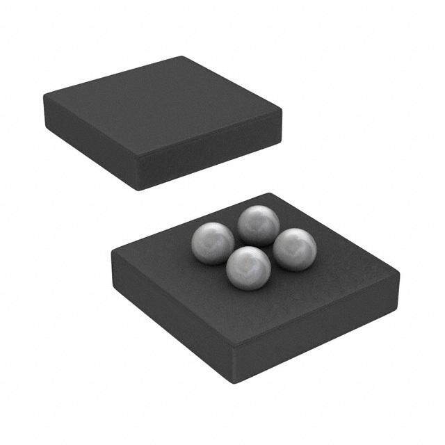
| 产品图片 |
|
| rohs | 符合RoHS无铅 / 符合限制有害物质指令(RoHS)规范要求 |
| 产品系列 | 板上安装温度传感器,Texas Instruments LM94022QBIMG/NOPBPowerWise® |
| 数据手册 | |
| 产品型号 | LM94022QBIMG/NOPB |
| 产品目录页面 | |
| 产品种类 | 板上安装温度传感器 |
| 供应商器件封装 | SC-70-5 |
| 关闭 | Shutdown |
| 其它名称 | *LM94022QBIMG/NOPB |
| 准确性 | +/- 2.7 C |
| 制造商产品页 | http://www.ti.com/general/docs/suppproductinfo.tsp?distId=10&orderablePartNumber=LM94022QBIMG/NOPB |
| 包装 | 剪切带 (CT) |
| 商标 | Texas Instruments |
| 增益 | - 5.5 mV/C, - 8.2 mV/C, - 10.9 mV/C, -13.6 mV/C |
| 安装风格 | SMD/SMT |
| 封装 | Reel |
| 封装/外壳 | 6-TSSOP(5 引线),SC-88A,SOT-353 |
| 封装/箱体 | SC-70-5 |
| 工厂包装数量 | 1000 |
| 感应温度 | -50°C ~ 150°C |
| 数字输出-总线接口 | - |
| 最大工作温度 | + 150 C |
| 最小工作温度 | - 50 C |
| 标准包装 | 1 |
| 电压-电源 | 1.5 V ~ 5.5 V |
| 电源电压-最大 | 5.5 V |
| 电源电压-最小 | 1.5 V |
| 电源电流 | 5.4 uA |
| 精度 | ±2.7°C |
| 系列 | LM94022-Q1 |
| 设备功能 | Temperature Sensor |
| 输出电流 | 7 mA |
| 输出类型 | 推挽式 |
| 配用 | /product-detail/zh/SPUSI2%2FNOPB/SPUSI2%2FNOPB-ND/1975525/product-detail/zh/LM94022EVAL/LM94022EVAL-ND/1640828 |
| 配置 | Local |


- 商务部:美国ITC正式对集成电路等产品启动337调查
- 曝三星4nm工艺存在良率问题 高通将骁龙8 Gen1或转产台积电
- 太阳诱电将投资9.5亿元在常州建新厂生产MLCC 预计2023年完工
- 英特尔发布欧洲新工厂建设计划 深化IDM 2.0 战略
- 台积电先进制程称霸业界 有大客户加持明年业绩稳了
- 达到5530亿美元!SIA预计今年全球半导体销售额将创下新高
- 英特尔拟将自动驾驶子公司Mobileye上市 估值或超500亿美元
- 三星加码芯片和SET,合并消费电子和移动部门,撤换高东真等 CEO
- 三星电子宣布重大人事变动 还合并消费电子和移动部门
- 海关总署:前11个月进口集成电路产品价值2.52万亿元 增长14.8%


PDF Datasheet 数据手册内容提取
Product Sample & Technical Tools & Support & Folder Buy Documents Software Community LM94022,LM94022-Q1 SNIS140F–MAY2006–REVISEDSEPTEMBER2015 LM94022/-Q1 1.5-V, SC70, Multi-Gain Analog Temperature Sensor With Class-AB Output 1 Features 3 Description • LM94022/-Q1isAEC-Q100Grade0qualifiedand The LM94022/-Q1 device is a precision analog output 1 CMOS integrated-circuit temperature sensor with isManufacturedonanAutomotiveGradeFlow selectable linear negative temperature coefficient • Low1.5-Vto5.5-VOperationWithLow5.4-µA (NTC). A class-AB output structure gives the SupplyCurrent LM94022/-Q1 strong output source and sink current • Push-PullOutputWith ±50-µASourceCurrent capability for driving heavy transient loads such as Capability that presented by the input of a sample-and-hold analog-to-digital converter. The low 5.4-µA supply • FourSelectableGains current and 1.5-V operating voltage of the LM94022/- • VeryAccurateOverWideTemperatureRangeof Q1 make it ideal for battery-powered systems as well −50°Cto+150°C: asgeneraltemperature-sensingapplications. – ±1.5ºCTemperatureAccuracyfor20ºCto The Gain Select 1 (GS1) and Gain Select 0 (GS0) 40ºCRange logic inputs select one of four gains for the – ±1.8ºCTemperatureAccuracyfor–50ºCto temperature-to-voltage output transfer function: −5.5 70ºCRange mV/°C, −8.2 mV/°C, −10.9 mV/°C, and −13.6 mV/°C. Selecting –5.5 mV/°C (GS1 and GS0 both tied low), – ±2.1ºCTemperatureAccuracyfor–50ºCto allows the LM94022/-Q1 to operate down to 1.5-V 90ºCRange supply while measuring temperature over the full – ±2.7ºCTemperatureAccuracyfor–50ºCto range of −50°C to +150°C. Maximum temperature 150ºCRange sensitivity, –13.6 mV/°C, is selected when GS1 and • OutputisShort-CircuitProtected GS0 are both tied high. The gain-select inputs can be tied directly to V or Ground without any pullup or • ExtremelySmallSC70Package DD pulldown resistors, reducing component count and • FortheSimilarFunctionalityinaTO-92Package, board area. These inputs can also be driven by logic SeeLMT84,LMT85,LMT86,orLMT87 signals allowing the system to optimize the gain • FootprintCompatibleWiththeIndustry-Standard duringoperationorsystemdiagnostics. LM20TemperatureSensor DeviceInformation(1) 2 Applications PARTNUMBER PACKAGE BODYSIZE(NOM) LM94022 • Automotive SC70(5) 2.00mm×1.25mm LM94022-Q1 • CellPhones (1) For all available packages, see the orderable addendum at • WirelessTransceivers theendofthedatasheet. • BatteryManagement • DiskDrives • Games • Appliances Full-RangeCelsiusTemperatureSensor(–50°Cto OutputTemperatureCharacteristic +150°C)OperatingfromaSingleCellBattery VDD (+1.5V to +5.5V) VDD Single Battery LM94022 Cell GS1 OUT GS0 GND 1 An IMPORTANT NOTICE at the end of this data sheet addresses availability, warranty, changes, use in safety-critical applications, intellectualpropertymattersandotherimportantdisclaimers.PRODUCTIONDATA.
LM94022,LM94022-Q1 SNIS140F–MAY2006–REVISEDSEPTEMBER2015 www.ti.com Table of Contents 1 Features.................................................................. 1 8 ApplicationandImplementation........................ 16 2 Applications........................................................... 1 8.1 ApplicationInformation............................................16 3 Description............................................................. 1 8.2 TypicalApplication .................................................17 4 RevisionHistory..................................................... 2 8.3 SystemExamples...................................................18 5 PinConfigurationandFunctions......................... 3 9 PowerSupplyRecommendations...................... 19 6 Specifications......................................................... 4 10 Layout................................................................... 19 6.1 AbsoluteMaximumRatings......................................4 10.1 LayoutGuidelines.................................................19 6.2 ESDRatings..............................................................4 10.2 LayoutExample....................................................20 6.3 RecommendedOperatingConditions.......................4 10.3 OutputandNoiseConsiderations.........................20 6.4 ThermalInformation..................................................4 11 DeviceandDocumentationSupport................. 21 6.5 ElectricalCharacteristics..........................................5 11.1 RelatedLinks........................................................21 6.6 TypicalCharacteristics..............................................7 11.2 CommunityResources..........................................21 7 DetailedDescription.............................................. 9 11.3 Trademarks...........................................................21 7.1 Overview...................................................................9 11.4 ElectrostaticDischargeCaution............................21 7.2 FunctionalBlockDiagram.........................................9 11.5 Glossary................................................................21 7.3 FeatureDescription...................................................9 12 Mechanical,Packaging,andOrderable Information........................................................... 21 7.4 DeviceFunctionalModes........................................14 4 Revision History NOTE:Pagenumbersforpreviousrevisionsmaydifferfrompagenumbersinthecurrentversion. ChangesfromRevisionE(June2013)toRevisionF Page • Addedorchanged:PinConfigurationandFunctionssection,ESDRatingstable,FeatureDescriptionsection, DeviceFunctionalModes,ApplicationandImplementationsection,PowerSupplyRecommendationssection, Layoutsection,DeviceandDocumentationSupportsection,andMechanical,Packaging,andOrderableInformation section ................................................................................................................................................................................... 1 ChangesfromRevisionD(February2013)toRevisionE Page • addedparabolicequationforLM94022/-Q1 .......................................................................................................................... 1 ChangesfromRevisionC(May2005)toRevisionD Page • ChangedlayoutofNationalDataSheettoTIformat........................................................................................................... 17 2 SubmitDocumentationFeedback Copyright©2006–2015,TexasInstrumentsIncorporated ProductFolderLinks:LM94022 LM94022-Q1
LM94022,LM94022-Q1 www.ti.com SNIS140F–MAY2006–REVISEDSEPTEMBER2015 5 Pin Configuration and Functions DCKPackage 5-PinSC70 TopView 1 5 GS0 GS1 GND 2 LM94022 3 4 OUT VDD PinFunctions PIN TYPE EQUIVALENTCIRCUIT FUNCTION NAME NO. VDD GainSelect1-Oneoftwologicinputsforselecting GS1 5 LogicInput theslopeoftheoutputresponse ESD CLAMP GND GainSelect0-Oneoftwologicinputsforselecting GS0 1 LogicInput theslopeoftheoutputresponse VDD Outputsavoltagewhichisinverselyproportionalto OUT 3 AnalogOutput temperature GND V 4 Power — PositiveSupplyVoltage DD GND 2 Ground — PowerSupplyGround Copyright©2006–2015,TexasInstrumentsIncorporated SubmitDocumentationFeedback 3 ProductFolderLinks:LM94022 LM94022-Q1
LM94022,LM94022-Q1 SNIS140F–MAY2006–REVISEDSEPTEMBER2015 www.ti.com 6 Specifications 6.1 Absolute Maximum Ratings overoperatingfree-airtemperaturerange(unlessotherwisenoted)(1)(2) MIN MAX UNIT SupplyVoltage −0.3 6 V VoltageatOutputPin −0.3 (V +0.5) V DD OutputCurrent ±7 mA VoltageatGS0andGS1InputPins −0.3 6 V InputCurrentatanypin(3) 5 mA MaximumJunctionTemperature,T 150 °C JMAX Storagetemperature,T −65 150 °C stg (1) StressesbeyondthoselistedunderAbsoluteMaximumRatingsmaycausepermanentdamagetothedevice.Thesearestressratings only,whichdonotimplyfunctionaloperationofthedeviceattheseoranyotherconditionsbeyondthoseindicatedunderRecommended OperatingConditions.Exposuretoabsolute-maximum-ratedconditionsforextendedperiodsmayaffectdevicereliability. (2) SolderingprocessmustcomplywithReflowTemperatureProfilespecifications.Refertohttp://www.ti.com/packaging (3) Whentheinputvoltage(V)atanypinexceedspowersupplies(V <GNDorV >V+),thecurrentatthatpinshouldbelimitedto5mA. I I I 6.2 ESD Ratings VALUE UNIT Humanbodymodel(HBM)(1)(2) ±2500 V Electrostaticdischarge V (ESD) Machinemodel(2) ±250 (1) JEDECdocumentJEP155statesthat500-VHBMallowssafemanufacturingwithastandardESDcontrolprocess. (2) Thehumanbodymodelisa100-pFcapacitordischargedthrougha1.5-kΩresistorintoeachpin.Themachinemodelisa200-pF capacitordischargeddirectlyintoeachpin. 6.3 Recommended Operating Conditions overoperatingfree-airtemperaturerange(unlessotherwisenoted)(1) MIN MAX UNIT FreeAirorSpecifiedTemperature (T ≤T ≤T ) −50 150 °C MIN A MAX SupplyVoltage(V ) 1.5 5.5 V DD (1) AbsoluteMaximumRatingsindicatelimitsbeyondwhichdamagetothedevicemayoccur.OperatingRatingsindicateconditionsfor whichthedeviceisfunctional,butdonotguaranteespecificperformancelimits.Forguaranteedspecificationsandtestconditions,see theElectricalCharacteristics.Theguaranteedspecificationsapplyonlyforthetestconditionslisted.Someperformancecharacteristics maydegradewhenthedeviceisnotoperatedunderthelistedtestconditions. 6.4 Thermal Information LM94022,LM94022-Q1 THERMALMETRIC(1) DCK(SC70) UNIT 5PINS R Junction-to-ambientthermalresistance 415 °C/W θJA (1) Formoreinformationabouttraditionalandnewthermalmetrics,seetheSemiconductorandICPackageThermalMetricsapplication report,SPRA953. 4 SubmitDocumentationFeedback Copyright©2006–2015,TexasInstrumentsIncorporated ProductFolderLinks:LM94022 LM94022-Q1
LM94022,LM94022-Q1 www.ti.com SNIS140F–MAY2006–REVISEDSEPTEMBER2015 6.5 Electrical Characteristics Unlessotherwisenoted,thesespecificationsapplyforV =1.5Vto5.5V;alllimitsT =T =25°Cunlessotherwise DD A J specified.TheselimitsdonotincludeDCloadregulation.Thesestatedaccuracylimitsarewithreferencetothevaluesinthe Table2. PARAMETER CONDITIONS MIN TYP(1) MAX(2) UNIT ACCURACYCHARACTERISTICS T =+20°Cto+40°C; –1.5 1.5 A °C V =1.5Vto5.5V DD T =+0°Cto+70°C; –1.8 1.8 A °C V =1.5Vto5.5V DD T =+0°Cto+90°C; –2.1 2.1 A °C GS1=0 VDD=1.5Vto5.5V GS0=0 T =+0°Cto+120°C; –2.4 2.4 A °C V =1.5Vto5.5V DD T =+0°Cto+150°C; –2.7 2.7 A °C V =1.5Vto5.5V DD T =−50°Cto+0°C; –1.8 1.8 A °C V =1.6Vto5.5V DD T =+20°Cto+40°C; –1.5 1.5 A °C V =1.8Vto5.5V DD T =+0°Cto+70°C; –1.8 1.8 A °C V =1.9Vto5.5V DD T =+0°Cto+90°C; –2.1 2.1 A °C GS1=0 VDD=1.9Vto5.5V GS0=1 T =+0°Cto+120°C; –2.4 2.4 A °C V =1.9Vto5.5V DD T =+0°Cto+150°C; –2.7 2.7 A °C V =1.9Vto5.5V DD T =−50°Cto+0°C; –1.8 1.8 A °C V =2.3Vto5.5V TemperatureError(3) DD T =+20°Cto+40°C; –1.5 1.5 A °C V =2.2Vto5.5V DD T =+0°Cto+70°C; –1.8 1.8 A °C V =2.4Vto5.5V DD T =+0°Cto+90°C; –2.1 2.1 A °C GS1=1 VDD=2.4Vto5.5V GS0=0 T =+0°Cto+120°C; –2.4 2.4 A °C V =2.4Vto5.5V DD T =+0°Cto+150°C; –2.7 2.7 A °C V =2.4Vto5.5V DD T =−50°Cto+0°C; –1.8 1.8 A °C V =3.0Vto5.5V DD T =+20°Cto+40°C; –1.5 1.5 A °C V =2.7Vto5.5V DD T =+0°Cto+70°C; –1.8 1.8 A °C V =3.0Vto5.5V DD T =+0°Cto+90°C; –2.1 2.1 A °C GS1=1 VDD=3.0Vto5.5V GS0=1 T =+0°Cto+120°C; –2.4 2.4 A °C V =3.0Vto5.5V DD T =0°Cto+150°C; –2.7 2.7 A °C V =3.0Vto5.5V DD T =−50°Cto+0°C; –1.8 1.8 A °C V =3.6Vto5.5V DD (1) TypicalsareatT =T =25°Candrepresentmostlikelyparametricnorm. J A (2) LimitsarewarrantiedtoTI'sAOQL(AverageOutgoingQualityLevel). (3) Accuracyisdefinedastheerrorbetweenthemeasuredandreferenceoutputvoltages,tabulatedintheTransferTableatthespecified conditionsofsupplygainsetting,voltage,andtemperature(expressedin°C).Accuracylimitsincludelineregulationwithinthespecified conditions.Accuracylimitsdonotincludeloadregulation;theyassumenoDCload. Copyright©2006–2015,TexasInstrumentsIncorporated SubmitDocumentationFeedback 5 ProductFolderLinks:LM94022 LM94022-Q1
LM94022,LM94022-Q1 SNIS140F–MAY2006–REVISEDSEPTEMBER2015 www.ti.com Electrical Characteristics (continued) Unlessotherwisenoted,thesespecificationsapplyforV =1.5Vto5.5V;alllimitsT =T =25°Cunlessotherwise DD A J specified.TheselimitsdonotincludeDCloadregulation.Thesestatedaccuracylimitsarewithreferencetothevaluesinthe Table2. PARAMETER CONDITIONS MIN TYP(1) MAX(2) UNIT GS1=0,GS0=0 –5.5 mV/°C GS1=0,GS0=1 –8.2 mV/°C SensorGain GS1=1,GS0=0 –10.9 mV/°C GS1=1,GS0=1 –13.6 mV/°C Source≤50μA, –0.22 mV LoadRegulation(4) (VDD–VOUT)≥200mV TA=TJ=TMINtoTMAX –1 Sink≤50μA, 0.26 mV VOUT≥200mV TA=TJ=TMINtoTMAX 1 LineRegulation(5) 200 μV/V 5.4 (V –V )≥100mV μA DD OUT T =T =+30°Cto+150°C 8.1 A J I SupplyCurrent S 5.4 (V –V )≥100mV μA DD OUT T =T =T toT 9 A J MIN MAX C OutputLoadCapacitance 1100 pF L 0.7 Power-ONTime(6) C =0pFto1100pF ms L T =T =T toT 1.9 A J MIN MAX GS1andGS0InputLogic V T =T =T toT V –0.5 V IH 1ThresholdVoltage A J MIN MAX DD GS1andGS0InputLogic V T =T =T toT 0.5 V IL 0ThresholdVoltage A J MIN MAX 0.001 I Logic1InputCurrent(7) μA IH T =T =T toT 1 A J MIN MAX 0.001 I Logic0InputCurrent(7) μA IL T =T =T toT 1 A J MIN MAX (4) SourcecurrentsareflowingoutoftheLM94022/-Q1.SinkcurrentsareflowingintotheLM94022/-Q1. (5) Lineregulation(DC)iscalculatedbysubtractingtheoutputvoltageatthehighestsupplyvoltagefromtheoutputvoltageatthelowest supplyvoltage.ThetypicalDClineregulationspecificationdoesnotincludetheoutputvoltageshiftdiscussedinOutputVoltageShift. (6) Warrantiedbydesignandcharacterization. (7) Theinputcurrentisleakageonlyandishighestathightemperature.Itistypicallyonly0.001µA.The1-µAlimitissolelybasedona testinglimitationanddoesnotreflecttheactualperformanceofthepart. 6 SubmitDocumentationFeedback Copyright©2006–2015,TexasInstrumentsIncorporated ProductFolderLinks:LM94022 LM94022-Q1
LM94022,LM94022-Q1 www.ti.com SNIS140F–MAY2006–REVISEDSEPTEMBER2015 6.6 Typical Characteristics 4 MAX Limit 3 C) R (º 2 O R 1 R E RE 0 MIN Limit U T A -1 R E P -2 M E T -3 -4 -50 -25 0 25 50 75 100 125 150 TEMPERATURE (ºC) Figure1.TemperatureErrorvs.Temperature Figure2.MinimumOperatingTemperaturevs.Supply Voltage Figure3.SupplyCurrentvs.Temperature Figure4.SupplyCurrentvs.SupplyVoltage Figure5.LoadRegulation,SourcingCurrent Figure6.LoadRegulation,SinkingCurrent Copyright©2006–2015,TexasInstrumentsIncorporated SubmitDocumentationFeedback 7 ProductFolderLinks:LM94022 LM94022-Q1
LM94022,LM94022-Q1 SNIS140F–MAY2006–REVISEDSEPTEMBER2015 www.ti.com Typical Characteristics (continued) Figure7.ChangeinVoutvs.OverheadVoltage Figure8.Supply-NoiseGainvs.Frequency Figure9.OutputVoltagevs.SupplyVoltage Figure10.OutputVoltagevs.SupplyVoltage GainSelect=00 GainSelect=01 Figure11.OutputVoltagevs.SupplyVoltage Figure12.OutputVoltagevs.SupplyVoltage GainSelect=10 GainSelect=11 8 SubmitDocumentationFeedback Copyright©2006–2015,TexasInstrumentsIncorporated ProductFolderLinks:LM94022 LM94022-Q1
LM94022,LM94022-Q1 www.ti.com SNIS140F–MAY2006–REVISEDSEPTEMBER2015 7 Detailed Description 7.1 Overview The LM94022/-Q1 is an analog output temperature sensor with a selectable negative temperature coefficient output (NTC). The temperature-sensing element is comprised of stacked transistor base emitter junctions (thermal diodes) that are forward biased by a current source. The number of stacked thermal diodes determines the output gain or slope. The gain select pins (GS1 and GS0) are simple logic inputs that control the number of stacked thermal diodes thus selecting the output gain as shown in the Table 1 table. The temperature sensing element is buffered by a simple amplifier that drives the output pin. The simple class AB output stage of the amplifiercansourceorsinkcurrentandprovideslow-impedance,high-currentdrive. Table1.GainSelectPinFunction GS1LOGIC GS0LOGIC SELECTEDAVERAGEGAIN LEVEL LEVEL 0 0 –5.5mV/°C 0 1 –8.2mV/°C 1 0 –10.9mV/°C 1 1 –13.6mV/°C 7.2 Functional Block Diagram VDD LM94022 OUT Thermal Diodes GS1 Gain Select Logic GS0 GND 7.3 Feature Description 7.3.1 LM94022/-Q1TransferFunctionGainSelection The LM94022/-Q1 has four selectable gains, each of which can be selected by the GS1 and GS0 input pins. The output voltage for each gain, across the complete operating temperature range is shown in Table 2. This table is the reference from which the LM94022/-Q1 accuracy specifications (listed in the Electrical Characteristics section) are determined. This table can be used, for example, in a host processor look-up table. A file containing thisdataisavailablefordownloadatLM94022productfolderunderToolsandSoftware. Copyright©2006–2015,TexasInstrumentsIncorporated SubmitDocumentationFeedback 9 ProductFolderLinks:LM94022 LM94022-Q1
LM94022,LM94022-Q1 SNIS140F–MAY2006–REVISEDSEPTEMBER2015 www.ti.com Table2.LM94022/LM94022-Q1TransferTable TEMPERATURE GS=00 GS=01 GS=10 GS=11 (°C) (mV) (mV) (mV) (mV) –50 1299 1955 2616 3277 –49 1294 1949 2607 3266 –48 1289 1942 2598 3254 –47 1284 1935 2589 3243 –46 1278 1928 2580 3232 –45 1273 1921 2571 3221 –44 1268 1915 2562 3210 –43 1263 1908 2553 3199 –42 1257 1900 2543 3186 –41 1252 1892 2533 3173 –40 1247 1885 2522 3160 –39 1242 1877 2512 3147 –38 1236 1869 2501 3134 –37 1231 1861 2491 3121 –36 1226 1853 2481 3108 –35 1221 1845 2470 3095 –34 1215 1838 2460 3082 –33 1210 1830 2449 3069 –32 1205 1822 2439 3056 –31 1200 1814 2429 3043 –30 1194 1806 2418 3030 –29 1189 1798 2408 3017 –28 1184 1790 2397 3004 –27 1178 1783 2387 2991 –26 1173 1775 2376 2978 –25 1168 1767 2366 2965 –24 1162 1759 2355 2952 –23 1157 1751 2345 2938 –22 1152 1743 2334 2925 –21 1146 1735 2324 2912 –20 1141 1727 2313 2899 –19 1136 1719 2302 2886 –18 1130 1711 2292 2873 –17 1125 1703 2281 2859 –16 1120 1695 2271 2846 –15 1114 1687 2260 2833 –14 1109 1679 2250 2820 –13 1104 1671 2239 2807 –12 1098 1663 2228 2793 –11 1093 1656 2218 2780 –10 1088 1648 2207 2767 –9 1082 1639 2197 2754 –8 1077 1631 2186 2740 –7 1072 1623 2175 2727 –6 1066 1615 2164 2714 –5 1061 1607 2154 2700 –4 1055 1599 2143 2687 10 SubmitDocumentationFeedback Copyright©2006–2015,TexasInstrumentsIncorporated ProductFolderLinks:LM94022 LM94022-Q1
LM94022,LM94022-Q1 www.ti.com SNIS140F–MAY2006–REVISEDSEPTEMBER2015 Table2.LM94022/LM94022-Q1TransferTable(continued) TEMPERATURE GS=00 GS=01 GS=10 GS=11 (°C) (mV) (mV) (mV) (mV) –3 1050 1591 2132 2674 –2 1044 1583 2122 2660 –1 1039 1575 2111 2647 0 1034 1567 2100 2633 1 1028 1559 2089 2620 2 1023 1551 2079 2607 3 1017 1543 2068 2593 4 1012 1535 2057 2580 5 1007 1527 2047 2567 6 1001 1519 2036 2553 7 996 1511 2025 2540 8 990 1502 2014 2527 9 985 1494 2004 2513 10 980 1486 1993 2500 11 974 1478 1982 2486 12 969 1470 1971 2473 13 963 1462 1961 2459 14 958 1454 1950 2446 15 952 1446 1939 2433 16 947 1438 1928 2419 17 941 1430 1918 2406 18 936 1421 1907 2392 19 931 1413 1896 2379 20 925 1405 1885 2365 21 920 1397 1874 2352 22 914 1389 1864 2338 23 909 1381 1853 2325 24 903 1373 1842 2311 25 898 1365 1831 2298 26 892 1356 1820 2285 27 887 1348 1810 2271 28 882 1340 1799 2258 29 876 1332 1788 2244 30 871 1324 1777 2231 31 865 1316 1766 2217 32 860 1308 1756 2204 33 854 1299 1745 2190 34 849 1291 1734 2176 35 843 1283 1723 2163 36 838 1275 1712 2149 37 832 1267 1701 2136 38 827 1258 1690 2122 39 821 1250 1679 2108 40 816 1242 1668 2095 41 810 1234 1657 2081 42 804 1225 1646 2067 43 799 1217 1635 2054 Copyright©2006–2015,TexasInstrumentsIncorporated SubmitDocumentationFeedback 11 ProductFolderLinks:LM94022 LM94022-Q1
LM94022,LM94022-Q1 SNIS140F–MAY2006–REVISEDSEPTEMBER2015 www.ti.com Table2.LM94022/LM94022-Q1TransferTable(continued) TEMPERATURE GS=00 GS=01 GS=10 GS=11 (°C) (mV) (mV) (mV) (mV) 44 793 1209 1624 2040 45 788 1201 1613 2026 46 782 1192 1602 2012 47 777 1184 1591 1999 48 771 1176 1580 1985 49 766 1167 1569 1971 50 760 1159 1558 1958 51 754 1151 1547 1944 52 749 1143 1536 1930 53 743 1134 1525 1916 54 738 1126 1514 1902 55 732 1118 1503 1888 56 726 1109 1492 1875 57 721 1101 1481 1861 58 715 1093 1470 1847 59 710 1084 1459 1833 60 704 1076 1448 1819 61 698 1067 1436 1805 62 693 1059 1425 1791 63 687 1051 1414 1777 64 681 1042 1403 1763 65 676 1034 1391 1749 66 670 1025 1380 1735 67 664 1017 1369 1721 68 659 1008 1358 1707 69 653 1000 1346 1693 70 647 991 1335 1679 71 642 983 1324 1665 72 636 974 1313 1651 73 630 966 1301 1637 74 625 957 1290 1623 75 619 949 1279 1609 76 613 941 1268 1595 77 608 932 1257 1581 78 602 924 1245 1567 79 596 915 1234 1553 80 591 907 1223 1539 81 585 898 1212 1525 82 579 890 1201 1511 83 574 881 1189 1497 84 568 873 1178 1483 85 562 865 1167 1469 86 557 856 1155 1455 87 551 848 1144 1441 88 545 839 1133 1427 89 539 831 1122 1413 90 534 822 1110 1399 12 SubmitDocumentationFeedback Copyright©2006–2015,TexasInstrumentsIncorporated ProductFolderLinks:LM94022 LM94022-Q1
LM94022,LM94022-Q1 www.ti.com SNIS140F–MAY2006–REVISEDSEPTEMBER2015 Table2.LM94022/LM94022-Q1TransferTable(continued) TEMPERATURE GS=00 GS=01 GS=10 GS=11 (°C) (mV) (mV) (mV) (mV) 91 528 814 1099 1385 92 522 805 1088 1371 93 517 797 1076 1356 94 511 788 1065 1342 95 505 779 1054 1328 96 499 771 1042 1314 97 494 762 1031 1300 98 488 754 1020 1286 99 482 745 1008 1272 100 476 737 997 1257 101 471 728 986 1243 102 465 720 974 1229 103 459 711 963 1215 104 453 702 951 1201 105 448 694 940 1186 106 442 685 929 1172 107 436 677 917 1158 108 430 668 906 1144 109 425 660 895 1130 110 419 651 883 1115 111 413 642 872 1101 112 407 634 860 1087 113 401 625 849 1073 114 396 617 837 1058 115 390 608 826 1044 116 384 599 814 1030 117 378 591 803 1015 118 372 582 791 1001 119 367 573 780 987 120 361 565 769 973 121 355 556 757 958 122 349 547 745 944 123 343 539 734 929 124 337 530 722 915 125 332 521 711 901 126 326 513 699 886 127 320 504 688 872 128 314 495 676 858 129 308 487 665 843 130 302 478 653 829 131 296 469 642 814 132 291 460 630 800 133 285 452 618 786 134 279 443 607 771 135 273 434 595 757 136 267 425 584 742 137 261 416 572 728 Copyright©2006–2015,TexasInstrumentsIncorporated SubmitDocumentationFeedback 13 ProductFolderLinks:LM94022 LM94022-Q1
LM94022,LM94022-Q1 SNIS140F–MAY2006–REVISEDSEPTEMBER2015 www.ti.com Table2.LM94022/LM94022-Q1TransferTable(continued) TEMPERATURE GS=00 GS=01 GS=10 GS=11 (°C) (mV) (mV) (mV) (mV) 138 255 408 560 713 139 249 399 549 699 140 243 390 537 684 141 237 381 525 670 142 231 372 514 655 143 225 363 502 640 144 219 354 490 626 145 213 346 479 611 146 207 337 467 597 147 201 328 455 582 148 195 319 443 568 149 189 310 432 553 150 183 301 420 538 7.4 Device Functional Modes 7.4.1 CapacitiveLoads The LM94022/-Q1 handles capacitive loading well. In an extremely noisy environment, or when driving a switched sampling input on an ADC, it may be necessary to add some filtering to minimize noise coupling. Withoutanyprecautions,theLM94022/-Q1candriveacapacitiveloadlessthanorequalto1100pFasshownin Figure 13. For capacitive loads greater than 1100 pF, a series resistor may be required on the output, as shown inFigure14. VDD LM94022 OUT OPTIONAL BYPASS GND CLOAD < 1100 pF CAPACITANCE Figure13. LM94022/-Q1NoDecouplingRequiredforCapacitiveLoadsLessthan1100pF VDD RS LM94022 OUT OPTIONAL BYPASS GND CAPACITANCE CLOAD > 1100 pF Figure14. LM94022/-Q1WithSeriesResistorforCapacitiveLoadingGreaterthan1100pF C MINIMUMR LOAD S 1.1nFto99nF 3kΩ 100nFto999nF 1.5kΩ 1μF 800Ω 14 SubmitDocumentationFeedback Copyright©2006–2015,TexasInstrumentsIncorporated ProductFolderLinks:LM94022 LM94022-Q1
LM94022,LM94022-Q1 www.ti.com SNIS140F–MAY2006–REVISEDSEPTEMBER2015 7.4.2 OutputVoltageShift The LM94022/-Q1 is very linear over temperature and supply voltage range. Due to the intrinsic behavior of an NMOS/PMOS rail-to-rail buffer, a slight shift in the output can occur when the supply voltage is ramped over the operating range of the device. The location of the shift is determined by the relative levels of V and V . The DD OUT shifttypicallyoccurswhenV –V =1V. DD OUT This slight shift (a few mV) takes place over a wide change (approximately 200 mV) in V or V . Because the DD OUT shift takes place over a wide temperature change of 5°C to 20°C, V is always monotonic. The accuracy OUT specificationsintheElectricalCharacteristicstablealreadyincludethispossibleshift. 7.4.3 SelectableGainforOptimizationandinSituTesting TheGainSelectdigitalinputscanbetiedtotherailsorcanbedrivenfromdigitaloutputssuchasmicrocontroller GPIO pins. In low-supply voltage applications, the ability to reduce the gain to –5.5 mV/°C allows the LM94022/- Q1 to operate over the full –50°C to 150°C range. When a larger supply voltage is present, the gain can be increasedashighas–13.6mV/°C.Thelargergainisoptimalforreducingtheeffectsofnoise(forexample,noise coupling on the output line or quantization noise induced by an analog-to-digital converter which may be samplingtheLM94022/-Q1output). Another application advantage of the digitally selectable gain is the ability to perform dynamic testing of the LM94022/-Q1 while it is running in a system. By toggling the logic levels of the gain select pins and monitoring theresultantchangeintheoutputvoltagelevel,thehostsystemcanverifythefunctionalityoftheLM94022/-Q1. Copyright©2006–2015,TexasInstrumentsIncorporated SubmitDocumentationFeedback 15 ProductFolderLinks:LM94022 LM94022-Q1
LM94022,LM94022-Q1 SNIS140F–MAY2006–REVISEDSEPTEMBER2015 www.ti.com 8 Application and Implementation NOTE Information in the following applications sections is not part of the TI component specification, and TI does not warrant its accuracy or completeness. TI’s customers are responsible for determining suitability of components for their purposes. Customers should validateandtesttheirdesignimplementationtoconfirmsystemfunctionality. 8.1 Application Information The LM94022/-Q1 features make it suitable for many general temperature sensing applications. It can operate over a supply range of 1.5 V to 5.5 V with programmable output slope and a wide –50°C to +150°C temperature range,thusallowingflexibilityfordifferenttemperatureandsupplyvoltagerangecombinations. 8.1.1 LM94022TransferFunction The LM94022 has four selectable gains, each of which can be selected by the GS1 and GS0 input pins. The output voltage for each gain, across the complete operating temperature range is shown in Table 2. This table is thereferencefromwhichtheLM94022accuracyspecifications(listedintheElectricalCharacteristicssection)are determined. Although the LM94022 transfer curves are very linear, they do have a slight umbrella parabolic shape. This shapeisveryaccuratelyreflectedinTable2.Thetransfertablewasusedtocalculatethefollowingequations. J2,G00:V (cid:11)mV(cid:12)=870.6mV -5.506mV (cid:11)T -30°C(cid:12)-0.00176 mV (cid:11)T -30°C(cid:12)2 TEMP °C °C2 J3,G01:V (cid:11)mV(cid:12)=1324.0mV -8.194mV (cid:11)T -30°C(cid:12)-0.00262mV (cid:11)T -30°C(cid:12)2 TEMP °C °C2 J4,G10:V (cid:11)mV(cid:12)=1777.3mV -10.888mV (cid:11)T -30°C(cid:12)-0.00347 mV (cid:11)T -30°C(cid:12)2 TEMP °C °C2 J5,G11:V (cid:11)mV(cid:12)=2230.8mV -13.582mV (cid:11)T -30°C(cid:12)-0.00433mV (cid:11)T -30°C(cid:12)2 TEMP °C °C2 (1) A linear approximation can be useful over a narrow temperature range. A line can easily be calculated over the desiredtemperaturerangefromthetableusingthetwo-pointequation: ¹V2 - V1· V - V1 =·T2 - T1¹u(T - T1) where • VisinmV, • Tisin°C, • T andV arethecoordinatesofthelowesttemperature, 1 1 • T andV arethecoordinatesofthehighesttemperature. (2) 2 2 For example, to determine the equation of a line with the Gain Setting at GS1 = 0 and GS0 = 0, over a temperaturerangeof20°Cto50°C,proceedasfollows: ¹ · V - 925 mV = 760 mV - 925 mV u(T - 20oC) · 50oC - 20oC ¹ (3) V - 925 mV =(-5.50 mV / oC)u(T - 20oC) (4) V = (-5.50 mV / oC)u T + 1035 mV (5) Using this method of linear approximation, the transfer function can be approximated for one or more temperature ranges of interest. The accuracy will suffer slightly in favor of easy conversion of the output voltage totemperature. 16 SubmitDocumentationFeedback Copyright©2006–2015,TexasInstrumentsIncorporated ProductFolderLinks:LM94022 LM94022-Q1
LM94022,LM94022-Q1 www.ti.com SNIS140F–MAY2006–REVISEDSEPTEMBER2015 8.2 Typical Application SAR Analog-to-Digital Converter +1.5V to +5.5V Reset LM94022 Input Pin RIN Sample 4 3 VDD OUT CBP CIN GND 2 CFILTER CSAMPLE 5 1 GS1 GS0 Figure15. SuggestedConnectiontoaSamplingAnalog-to-DigitalConverterInputStage 8.2.1 DesignRequirements Most CMOS ADCs found in microcontrollers and ASICs have a sampled data comparator input structure. When the ADC charges the sampling cap, it requires instantaneous charge from the output of the analog source such as the LM94022/-Q1 temperature sensor and many op amps. This requirement is easily accommodated by the additionofacapacitorC ). FILTER 8.2.2 DetailedDesignProcedure The size of C depends on the size of the sampling capacitor and the sampling frequency. Since not all FILTER ADCs have identical input stages, the charge requirements will vary. This general ADC application is shown as anexampleonly. 8.2.3 ApplicationCurve Figure16. ProgrammableAnalogOutputTransferFunction Copyright©2006–2015,TexasInstrumentsIncorporated SubmitDocumentationFeedback 17 ProductFolderLinks:LM94022 LM94022-Q1
LM94022,LM94022-Q1 SNIS140F–MAY2006–REVISEDSEPTEMBER2015 www.ti.com 8.3 System Examples 8.3.1 ApplicationCircuits VDD (+1.5V to +5.5V) VDD Single Battery LM94022 Cell GS1 OUT GS0 GND Figure17. Full-RangeCelsiusTemperatureSensor(−50°Cto+150°C)OperatingfromaSingleBattery Cell V+ R3 VTEMP VT1 R4 VT2 4.1V R1 VT (High = overtemp alarm) +U1 VOUT VOUT LM4040 U3 0.1 PF - R2 (4.1)R2 VT1 = R1 + R2||R3 VDD LM94022 VTemp (4.1)R2 U2 VT2 = R2 + R1||R3 Figure18. CelsiusThermostat SHUTDOWN VDD LM94022 VOUT Any logic device output Figure19. ConservingPowerDissipationWithShutdown 18 SubmitDocumentationFeedback Copyright©2006–2015,TexasInstrumentsIncorporated ProductFolderLinks:LM94022 LM94022-Q1
LM94022,LM94022-Q1 www.ti.com SNIS140F–MAY2006–REVISEDSEPTEMBER2015 9 Power Supply Recommendations The LM94022/-Q1 low supply current and supply range of 1.5 V to 5.5 V allow the device to easily be powered frommanysources. Power supply bypassing is optional and is mainly dependent on the noise on the power supply. In noisy systems it may be necessary to add bypass capacitors to the lower the noise that couples to the output of the LM94022/- Q1. 10 Layout 10.1 Layout Guidelines 10.1.1 MountingandThermalConductivity The LM94022/-Q1 can be applied easily in the same way as other integrated-circuit temperature sensors. It can begluedorcementedtoasurface. To ensure good thermal conductivity, the backside of the LM94022/-Q1 die is directly attached to the GND pin (Pin 2). The temperatures of the lands and traces to the other leads of the LM94022/-Q1 will also affect the temperaturereading. Alternatively, the LM94022/-Q1 can be mounted inside a sealed-end metal tube, and can then be dipped into a bath or screwed into a threaded hole in a tank. As with any IC, the LM94022/-Q1 and accompanying wiring and circuits must be kept insulated and dry, to avoid leakage and corrosion. This is especially true if the circuit may operate at cold temperatures where condensation can occur. If moisture creates a short circuit from the output to ground or V , the output from the LM94022/-Q1 will not be correct. Printed-circuit coatings are often used to DD ensurethatmoisturecannotcorrodetheleadsorcircuittraces. The thermal resistance junction to ambient (θ ) is the parameter used to calculate the rise of a device junction JA temperature due to its power dissipation. The equation used to calculate the rise in the die temperature of the LM94022/-Q1is: TJ = TA + TJA [ ( V D D IQ ) + (V D D - V O ) I L ] where • T istheambienttemperature, A • I isthequiescentcurrent, Q • I istheloadcurrentontheoutput, L • andV istheoutputvoltage. (6) O Forexample,inanapplicationwhereT =30°C,V =5V,I =9 μA,GainSelect=11,V =2.231mV,and A DD DD OUT I = 2 μA, the junction temperature would be 30.021 °C, showing a self-heating error of only 0.021°C. Because L the junction temperature of the LM94022 is the actual temperature being measured, take care to minimize the load current that the LM94022/-Q1 is required to drive. Table 3 shows the thermal resistance of the LM94022/- Q1. Table3. LM94022/LM94022-Q1ThermalResistance DEVICENUMBER NSPACKAGENUMBER THERMALRESISTANCE(θ ) JA LM94022BIMG DCK0005A 415°C/W Copyright©2006–2015,TexasInstrumentsIncorporated SubmitDocumentationFeedback 19 ProductFolderLinks:LM94022 LM94022-Q1
LM94022,LM94022-Q1 SNIS140F–MAY2006–REVISEDSEPTEMBER2015 www.ti.com 10.2 Layout Example The LM94022/-Q1 is extremely simple to layout electrically. If a power supply bypass capacitor is used it should be connected as shown in Figure 20. The device pins and layout greatly influence the temperature that the LM94022/-Q1 die is measuring thus thermal modeling is recommended to ensure that the device is sensing the propertemperature. VIA to ground plane VIA to power plane VIA to power plane or ground plane GS0 GS1 GND OUT VDD 0.01µ F Figure20. RecommendedLayout 10.3 Output and Noise Considerations A push-pull output gives the LM94022/-Q1 the ability to sink and source significant current. This is beneficial when, for example, driving dynamic loads like an input stage on an analog-to-digital converter (ADC). In these applications the source current is required to quickly charge the input capacitor of the ADC. See the Application Circuits section for more discussion of this topic. The LM94022/-Q1 is ideal for this and other applications which requirestrongsourceorsinkcurrent. The supply-noise gain of the LM94022 (the ratio of the AC signal on V to the AC signal on V ) was OUT DD measured during bench tests. It is typical attenuation is shown in the Typical Characteristics section. A load capacitorontheoutputcanhelptofilternoise. For operation in very noisy environments, some bypass capacitance should be present on the supply within approximately2inchesoftheLM94022/-Q1. 20 SubmitDocumentationFeedback Copyright©2006–2015,TexasInstrumentsIncorporated ProductFolderLinks:LM94022 LM94022-Q1
LM94022,LM94022-Q1 www.ti.com SNIS140F–MAY2006–REVISEDSEPTEMBER2015 11 Device and Documentation Support 11.1 Related Links The table below lists quick access links. Categories include technical documents, support and community resources,toolsandsoftware,andquickaccesstosampleorbuy. Table4.RelatedLinks TECHNICAL TOOLS& SUPPORT& PARTS PRODUCTFOLDER SAMPLE&BUY DOCUMENTS SOFTWARE COMMUNITY LM94022 Clickhere Clickhere Clickhere Clickhere Clickhere LM94022-Q1 Clickhere Clickhere Clickhere Clickhere Clickhere 11.2 Community Resources The following links connect to TI community resources. Linked contents are provided "AS IS" by the respective contributors. They do not constitute TI specifications and do not necessarily reflect TI's views; see TI's Terms of Use. TIE2E™OnlineCommunity TI'sEngineer-to-Engineer(E2E)Community.Createdtofostercollaboration amongengineers.Ate2e.ti.com,youcanaskquestions,shareknowledge,exploreideasandhelp solveproblemswithfellowengineers. DesignSupport TI'sDesignSupport QuicklyfindhelpfulE2Eforumsalongwithdesignsupporttoolsand contactinformationfortechnicalsupport. 11.3 Trademarks E2EisatrademarkofTexasInstruments. Allothertrademarksarethepropertyoftheirrespectiveowners. 11.4 Electrostatic Discharge Caution Thesedeviceshavelimitedbuilt-inESDprotection.Theleadsshouldbeshortedtogetherorthedeviceplacedinconductivefoam duringstorageorhandlingtopreventelectrostaticdamagetotheMOSgates. 11.5 Glossary SLYZ022—TIGlossary. Thisglossarylistsandexplainsterms,acronyms,anddefinitions. 12 Mechanical, Packaging, and Orderable Information The following pages include mechanical, packaging, and orderable information. This information is the most current data available for the designated devices. This data is subject to change without notice and revision of thisdocument.Forbrowser-basedversionsofthisdatasheet,refertotheleft-handnavigation. Copyright©2006–2015,TexasInstrumentsIncorporated SubmitDocumentationFeedback 21 ProductFolderLinks:LM94022 LM94022-Q1
PACKAGE OPTION ADDENDUM www.ti.com 6-Feb-2020 PACKAGING INFORMATION Orderable Device Status Package Type Package Pins Package Eco Plan Lead/Ball Finish MSL Peak Temp Op Temp (°C) Device Marking Samples (1) Drawing Qty (2) (6) (3) (4/5) LM94022BIMG NRND SC70 DCK 5 1000 TBD Call TI Call TI -50 to 150 22B LM94022BIMG/NOPB ACTIVE SC70 DCK 5 1000 Green (RoHS SN Level-1-260C-UNLIM -50 to 150 22B & no Sb/Br) LM94022BIMGX/NOPB ACTIVE SC70 DCK 5 3000 Green (RoHS SN Level-1-260C-UNLIM -50 to 150 22B & no Sb/Br) LM94022QBIMG/NOPB ACTIVE SC70 DCK 5 1000 Green (RoHS SN Level-1-260C-UNLIM -50 to 150 22Q & no Sb/Br) LM94022QBIMGX/NOPB ACTIVE SC70 DCK 5 3000 Green (RoHS SN Level-1-260C-UNLIM -50 to 150 22Q & no Sb/Br) (1) The marketing status values are defined as follows: ACTIVE: Product device recommended for new designs. LIFEBUY: TI has announced that the device will be discontinued, and a lifetime-buy period is in effect. NRND: Not recommended for new designs. Device is in production to support existing customers, but TI does not recommend using this part in a new design. PREVIEW: Device has been announced but is not in production. Samples may or may not be available. OBSOLETE: TI has discontinued the production of the device. (2) RoHS: TI defines "RoHS" to mean semiconductor products that are compliant with the current EU RoHS requirements for all 10 RoHS substances, including the requirement that RoHS substance do not exceed 0.1% by weight in homogeneous materials. Where designed to be soldered at high temperatures, "RoHS" products are suitable for use in specified lead-free processes. TI may reference these types of products as "Pb-Free". RoHS Exempt: TI defines "RoHS Exempt" to mean products that contain lead but are compliant with EU RoHS pursuant to a specific EU RoHS exemption. Green: TI defines "Green" to mean the content of Chlorine (Cl) and Bromine (Br) based flame retardants meet JS709B low halogen requirements of <=1000ppm threshold. Antimony trioxide based flame retardants must also meet the <=1000ppm threshold requirement. (3) MSL, Peak Temp. - The Moisture Sensitivity Level rating according to the JEDEC industry standard classifications, and peak solder temperature. (4) There may be additional marking, which relates to the logo, the lot trace code information, or the environmental category on the device. (5) Multiple Device Markings will be inside parentheses. Only one Device Marking contained in parentheses and separated by a "~" will appear on a device. If a line is indented then it is a continuation of the previous line and the two combined represent the entire Device Marking for that device. (6) Lead/Ball Finish - Orderable Devices may have multiple material finish options. Finish options are separated by a vertical ruled line. Lead/Ball Finish values may wrap to two lines if the finish value exceeds the maximum column width. Addendum-Page 1
PACKAGE OPTION ADDENDUM www.ti.com 6-Feb-2020 Important Information and Disclaimer:The information provided on this page represents TI's knowledge and belief as of the date that it is provided. TI bases its knowledge and belief on information provided by third parties, and makes no representation or warranty as to the accuracy of such information. Efforts are underway to better integrate information from third parties. TI has taken and continues to take reasonable steps to provide representative and accurate information but may not have conducted destructive testing or chemical analysis on incoming materials and chemicals. TI and TI suppliers consider certain information to be proprietary, and thus CAS numbers and other limited information may not be available for release. In no event shall TI's liability arising out of such information exceed the total purchase price of the TI part(s) at issue in this document sold by TI to Customer on an annual basis. OTHER QUALIFIED VERSIONS OF LM94022, LM94022-Q1 : •Catalog: LM94022 •Automotive: LM94022-Q1 NOTE: Qualified Version Definitions: •Catalog - TI's standard catalog product •Automotive - Q100 devices qualified for high-reliability automotive applications targeting zero defects Addendum-Page 2
PACKAGE MATERIALS INFORMATION www.ti.com 29-Sep-2019 TAPE AND REEL INFORMATION *Alldimensionsarenominal Device Package Package Pins SPQ Reel Reel A0 B0 K0 P1 W Pin1 Type Drawing Diameter Width (mm) (mm) (mm) (mm) (mm) Quadrant (mm) W1(mm) LM94022BIMG SC70 DCK 5 1000 178.0 8.4 2.25 2.45 1.2 4.0 8.0 Q3 LM94022BIMG/NOPB SC70 DCK 5 1000 178.0 8.4 2.25 2.45 1.2 4.0 8.0 Q3 LM94022BIMGX/NOPB SC70 DCK 5 3000 178.0 8.4 2.25 2.45 1.2 4.0 8.0 Q3 LM94022QBIMG/NOPB SC70 DCK 5 1000 178.0 8.4 2.25 2.45 1.2 4.0 8.0 Q3 LM94022QBIMGX/NOPB SC70 DCK 5 3000 178.0 8.4 2.25 2.45 1.2 4.0 8.0 Q3 PackMaterials-Page1
PACKAGE MATERIALS INFORMATION www.ti.com 29-Sep-2019 *Alldimensionsarenominal Device PackageType PackageDrawing Pins SPQ Length(mm) Width(mm) Height(mm) LM94022BIMG SC70 DCK 5 1000 210.0 185.0 35.0 LM94022BIMG/NOPB SC70 DCK 5 1000 210.0 185.0 35.0 LM94022BIMGX/NOPB SC70 DCK 5 3000 210.0 185.0 35.0 LM94022QBIMG/NOPB SC70 DCK 5 1000 210.0 185.0 35.0 LM94022QBIMGX/NOPB SC70 DCK 5 3000 210.0 185.0 35.0 PackMaterials-Page2
None
None
IMPORTANTNOTICEANDDISCLAIMER TI PROVIDES TECHNICAL AND RELIABILITY DATA (INCLUDING DATASHEETS), DESIGN RESOURCES (INCLUDING REFERENCE DESIGNS), APPLICATION OR OTHER DESIGN ADVICE, WEB TOOLS, SAFETY INFORMATION, AND OTHER RESOURCES “AS IS” AND WITH ALL FAULTS, AND DISCLAIMS ALL WARRANTIES, EXPRESS AND IMPLIED, INCLUDING WITHOUT LIMITATION ANY IMPLIED WARRANTIES OF MERCHANTABILITY, FITNESS FOR A PARTICULAR PURPOSE OR NON-INFRINGEMENT OF THIRD PARTY INTELLECTUAL PROPERTY RIGHTS. These resources are intended for skilled developers designing with TI products. You are solely responsible for (1) selecting the appropriate TI products for your application, (2) designing, validating and testing your application, and (3) ensuring your application meets applicable standards, and any other safety, security, or other requirements. These resources are subject to change without notice. TI grants you permission to use these resources only for development of an application that uses the TI products described in the resource. Other reproduction and display of these resources is prohibited. No license is granted to any other TI intellectual property right or to any third party intellectual property right. TI disclaims responsibility for, and you will fully indemnify TI and its representatives against, any claims, damages, costs, losses, and liabilities arising out of your use of these resources. TI’s products are provided subject to TI’s Terms of Sale (www.ti.com/legal/termsofsale.html) or other applicable terms available either on ti.com or provided in conjunction with such TI products. TI’s provision of these resources does not expand or otherwise alter TI’s applicable warranties or warranty disclaimers for TI products. Mailing Address: Texas Instruments, Post Office Box 655303, Dallas, Texas 75265 Copyright © 2020, Texas Instruments Incorporated