ICGOO在线商城 > 传感器,变送器 > 温度传感器 - 模拟和数字输出 > TMP05AKSZ-500RL7
 Datasheet下载
- 型号: TMP05AKSZ-500RL7
- 制造商: Analog
- 库位|库存: xxxx|xxxx
- 要求:
| 数量阶梯 | 香港交货 | 国内含税 |
| +xxxx | $xxxx | ¥xxxx |
查看当月历史价格
查看今年历史价格
TMP05AKSZ-500RL7产品简介:
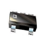
ICGOO电子元器件商城为您提供TMP05AKSZ-500RL7由Analog设计生产,在icgoo商城现货销售,并且可以通过原厂、代理商等渠道进行代购。 TMP05AKSZ-500RL7价格参考。AnalogTMP05AKSZ-500RL7封装/规格:温度传感器 - 模拟和数字输出, Temperature Sensor Digital, Local -40°C ~ 150°C SC-70-5。您可以下载TMP05AKSZ-500RL7参考资料、Datasheet数据手册功能说明书,资料中有TMP05AKSZ-500RL7 详细功能的应用电路图电压和使用方法及教程。
TMP05AKSZ-500RL7是Analog Devices Inc.推出的一款集成模拟和数字输出的温度传感器,适用于对精度和稳定性要求较高的应用场景。该器件具有±1°C的典型精度,支持单线数字接口和模拟电压输出,便于与微控制器或ADC直接连接,广泛用于工业控制、通信设备和消费电子等领域。

典型应用包括:精密仪器中的温度监控,确保系统在安全温度范围内运行;计算机和服务器中的CPU或电源模块热管理,防止过热导致性能下降或损坏;便携式医疗设备(如体温计、监护仪)中实现高可靠性体温监测;以及汽车电子中的环境温度检测,辅助电池管理系统或空调控制。

此外,TMP05AKSZ-500RL7采用小型SOIC封装,适合空间受限的设计,同时具备低功耗特性,适用于电池供电设备。其出厂校准特性减少了外部校准需求,提高了生产效率。综合来看,该传感器适用于需要兼顾模拟兼容性与数字通信能力的中高端温度监测场景。
| 参数 | 数值 |
| 产品目录 | 集成电路 (IC)热管理产品 |
| 描述 | IC PWM TEMP SNSR CMOS/TTL SC70-5板上安装温度传感器 IC +/-0.5 Deg/C Accurate PWM |
| 产品分类 | |
| 品牌 | Analog Devices Inc |
| 产品手册 | |
| 产品图片 |
|
| rohs | 符合RoHS无铅 / 符合限制有害物质指令(RoHS)规范要求 |
| 产品系列 | 板上安装温度传感器,Analog Devices TMP05AKSZ-500RL7- |
| 数据手册 | |
| 产品型号 | TMP05AKSZ-500RL7 |
| PCN设计/规格 | |
| 产品目录页面 | |
| 产品种类 | 板上安装温度传感器 |
| 传感器类型 | 内部 |
| 供应商器件封装 | SC-70-5 |
| 关闭 | No Shutdown |
| 其它名称 | TMP05AKSZ-500RL7DKR |
| 准确性 | 2 C |
| 功能 | 温度监控系统(传感器) |
| 包装 | Digi-Reel® |
| 商标 | Analog Devices |
| 安装类型 | 表面贴装 |
| 安装风格 | SMD/SMT |
| 封装 | Reel |
| 封装/外壳 | 6-TSSOP(5 引线),SC-88A,SOT-353 |
| 封装/箱体 | SC-70-5 |
| 工作温度 | -40°C ~ 150°C |
| 工厂包装数量 | 500 |
| 感应温度 | -40°C ~ 150°C |
| 拓扑 | ADC, 均值控制 |
| 最大工作温度 | + 150 C |
| 最小工作温度 | - 40 C |
| 标准包装 | 1 |
| 电压-电源 | 3 V ~ 5.5 V |
| 电源电压-最大 | 5.5 V |
| 电源电压-最小 | 3 V |
| 精度 | ±5°C(最大) |
| 系列 | TMP05 |
| 视频文件 | http://www.digikey.cn/classic/video.aspx?PlayerID=1364138032001&width=640&height=505&videoID=2245193158001http://www.digikey.cn/classic/video.aspx?PlayerID=1364138032001&width=640&height=505&videoID=1706665791001 |
| 设备功能 | Temperature Sensor |
| 输出报警 | 无 |
| 输出类型 | CMOS/TTL |
| 输出风扇 | 无 |
| 配置 | Local |


- 商务部:美国ITC正式对集成电路等产品启动337调查
- 曝三星4nm工艺存在良率问题 高通将骁龙8 Gen1或转产台积电
- 太阳诱电将投资9.5亿元在常州建新厂生产MLCC 预计2023年完工
- 英特尔发布欧洲新工厂建设计划 深化IDM 2.0 战略
- 台积电先进制程称霸业界 有大客户加持明年业绩稳了
- 达到5530亿美元!SIA预计今年全球半导体销售额将创下新高
- 英特尔拟将自动驾驶子公司Mobileye上市 估值或超500亿美元
- 三星加码芯片和SET,合并消费电子和移动部门,撤换高东真等 CEO
- 三星电子宣布重大人事变动 还合并消费电子和移动部门
- 海关总署:前11个月进口集成电路产品价值2.52万亿元 增长14.8%


PDF Datasheet 数据手册内容提取
±0.5°C Accurate PWM Temperature Sensor in 5-Lead SC-70 Data Sheet TMP05/TMP06 FEATURES FUNCTIONAL BLOCK DIAGRAM Modulated serial digital output, proportional to VDD temperature 5 ±0.5°C typical accuracy at 25°C TMP05/TMP06 ±1.0°C accuracy from 0°C to 70°C TEMPERATURE Two grades available SENSOR Σ-∆ AVERAGING CORE BLOCK/ 1 OUT Operation from −40°C to +150°C COUNTER REFERENCE Operation from 3 V to 5.5 V Power consumption 70 μW maximum at 3.3 V OUTPUT CMOS-/TTL-compatible output on TMP05 CONTROL CLKAND Flexible open-drain output on TMP06 CONV/IN 2 TIMING GENERATION Small, low cost, 5-lead SC-70 and SOT-23 packages 3 FUNC APPLICATIONS GN4D 03340-001 Isolated sensors Figure 1. Environmental control systems Computer thermal monitoring Thermal protection Industrial process control Power-system monitors GENERAL DESCRIPTION The CONV/IN input pin is used to determine the rate at which the TMP05/TMP06 measure temperature in continuously The TMP05/TMP06 are monolithic temperature sensors that converting mode and one shot mode. In daisy-chain mode, the generate a modulated serial digital output (PWM), which varies CONV/IN pin operates as the input to the daisy chain. in direct proportion to the temperature of the devices. The high period (T ) of the PWM remains static over all temperatures, PRODUCT HIGHLIGHTS H while the low period (T) varies. The B Grade version offers a L 1. The TMP05/TMP06 have an on-chip temperature sensor high temperature accuracy of ±1°C from 0°C to 70°C with that allows an accurate measurement of the ambient excellent transducer linearity. The digital output of the TMP05/ temperature. The measurable temperature range is TMP06 is CMOS-/TTL-compatible and is easily interfaced to –40°C to +150°C. the serial inputs of most popular microprocessors. The flexible open-drain output of the TMP06 is capable of sinking 5 mA. 2. Supply voltage is 3 V to 5.5 V. The TMP05/TMP06 are specified for operation at supply voltages 3. Space-saving 5-lead SOT-23 and SC-70 packages. from 3 V to 5.5 V. Operating at 3.3 V, the supply current is typically 370 μA. The TMP05/TMP06 are rated for operation over the –40°C 4. Temperature accuracy is typically ±0.5°C. Each part needs to +150°C temperature range. It is not recommended to operate a decoupling capacitor to achieve this accuracy. these devices at temperatures above 125°C for more than a total 5. Temperature resolution of 0.025°C. of 5% (5,000 hours) of the lifetime of the devices. They are packaged in low cost, low area SC-70 and SOT-23 packages. 6. The TMP05/TMP06 feature a one shot mode that reduces the average power consumption to 102 μW at 1 SPS. The TMP05/TMP06 have three modes of operation: continu- ously converting mode, daisy-chain mode, and one shot mode. A three-state FUNC input determines the mode in which the TMP05/TMP06 operate. Rev. C Information furnished by Analog Devices is believed to be accurate and reliable. However, no responsibility is assumed by Analog Devices for its use, nor for any infringements of patents or other One Technology Way, P.O. Box 9106, Norwood, MA 02062-9106, U.S.A. rights of third parties that may result from its use. Specifications subject to change without notice. No license is granted by implication or otherwise under any patent or patent rights of Analog Tel: 781.329.4700 www.analog.com Devices. Trademarks and registered trademarks are the property of their respective owners. Fax: 781.461.3113 ©2004–2012 Analog Devices, Inc. All rights reserved.
TMP05/TMP06 Data Sheet TABLE OF CONTENTS Features .............................................................................................. 1 Converter Details ....................................................................... 13 Applications ....................................................................................... 1 Functional Description .............................................................. 13 Functional Block Diagram .............................................................. 1 Operating Modes ........................................................................ 13 General Description ......................................................................... 1 TMP05 Output ........................................................................... 16 Product Highlights ........................................................................... 1 TMP06 Output ........................................................................... 16 Revision History ............................................................................... 2 Application Hints ........................................................................... 17 Specifications ..................................................................................... 3 Thermal Response Time ........................................................... 17 TMP05A/TMP06A Specifications ............................................. 3 Self-Heating Effects .................................................................... 17 TMP05B/TMP06B Specifications .............................................. 5 Supply Decoupling ..................................................................... 17 Timing Characteristics ................................................................ 7 Layout Considerations ............................................................... 18 Absolute Maximum Ratings ............................................................ 8 Temperature Monitoring ........................................................... 18 ESD Caution .................................................................................. 8 Daisy-Chain Application ........................................................... 18 Pin Configuration and Function Descriptions ............................. 9 Continuously Converting Application .................................... 24 Typical Performance Characteristics ........................................... 10 Outline Dimensions ....................................................................... 26 Theory of Operation ...................................................................... 13 Ordering Guide .......................................................................... 26 Circuit Information .................................................................... 13 REVISION HISTORY 8/12—Rev. B to Rev. C 10/05—Rev. 0 to Rev. A Changes to Table 1 ............................................................................ 3 Changes to Specifications Table ...................................................... 3 Changes to Table 2 ............................................................................ 5 Changes to Absolute Maximum Ratings ........................................ 8 Changes to Table 3 ............................................................................ 7 Changes to Figure 4 ........................................................................... 8 Changes to Figure 6, Figure 7, and Figure 8................................ 10 Changes to Figure 7 ........................................................................ 10 Changes to Figure 15 ...................................................................... 11 Changes to Figure 15 ...................................................................... 11 Changes to Functional Description Section ............................... 13 Deleted Figure 18 ............................................................................ 12 Changes to Table 7 and Table 8 ..................................................... 14 Changes to One Shot Mode Section ............................................ 14 Changes to Table 9 and Daisy-Chain Mode Section.................. 15 Changes to Figure 20 ...................................................................... 14 Updated Outline Dimensions ....................................................... 26 Changes to Daisy-Chain Mode Section....................................... 15 Changes to Figure 23 ...................................................................... 15 4/06—Rev. A to Rev. B Changes to Equation 5 and Equation 7 ....................................... 17 Changes to Table 1 ............................................................................ 3 Added Layout Considerations Section ........................................ 18 Changes to Table 2 ............................................................................ 5 Updated Outline Dimensions ....................................................... 26 Changes to Table 8 .......................................................................... 14 Changes to Ordering Guide .......................................................... 26 Changes to Table 9 .......................................................................... 15 8/04—Revision 0: Initial Version Rev. C | Page 2 of 28
Data Sheet TMP05/TMP06 SPECIFICATIONS TMP05A/TMP06A SPECIFICATIONS All A grade specifications apply for −40°C to +150°C, V decoupling capacitor is a 0.1 µF multilayer ceramic, T = T to T , DD A MIN MAX V = 3.0 V to 5.5 V, unless otherwise noted. DD Table 1. Parameter Min Typ Max Unit Test Conditions/Comments TEMPERATURE SENSOR AND ADC Nominal Conversion Rate (One Shot Mode) See Table 7 Accuracy @ V = 3.0 V to 5.5 V ±2 °C T = 0°C to 70°C, V = 3.0 V to 5.5 V DD A DD ±3 °C T = –40°C to +100°C, V = 3.0 V to 5.5 V A DD ±4 °C T = –40°C to +125°C, V = 3.0 V to 5.5 V A DD ±51 °C T = –40°C to +150°C, V = 3.0 V to 5.5 V A DD Temperature Resolution 0.025 °C/5 µs Step size for every 5 µs on T L T Pulse Width 34 ms T = 25°C, nominal conversion rate H A T Pulse Width 65 ms T = 25°C, nominal conversion rate L A Quarter Period Conversion Rate (All Operating Modes) See Table 7 Accuracy @ V = 3.3 V (3.0 V to 3.6 V) ±1.5 °C T = –40°C to +150°C DD A @ V = 5 V (4.5 V to 5.5 V) ±1.5 °C T = –40°C to +150°C DD A Temperature Resolution 0.1 °C/5 µs Step size for every 5 µs on T L T Pulse Width 8.5 ms T = 25°C, QI conversion rate H A T Pulse Width 16 ms T = 25°C, QP conversion rate L A Double High/Quarter Low Conversion Rate (All Operating Modes) See Table 7 Accuracy @ V = 3.3 V (3.0 V to 3.6 V) ±1.5 °C T = –40°C to +150°C DD A @ V = 5 V (4.5 V to 5.5 V) ±1.5 °C T = –40°C to +150°C DD A Temperature Resolution 0.1 °C/5 µs Step size for every 5 µs on T L T Pulse Width 68 ms T = 25°C, DH/QL conversion rate H A T Pulse Width 16 ms T = 25°C, DH/QL conversion rate L A Long-Term Drift 0.081 °C Drift over 10 years, if part is operated at 55°C Temperature Hysteresis 0.0023 °C Temperature cycle = 25°C to 100°C to 25°C SUPPLIES Supply Voltage 3 5.5 V Supply Current Normal Mode2 @ 3.3 V 370 600 µA Nominal conversion rate @ 5.0 V 425 650 µA Nominal conversion rate Quiescent2 @ 3.3 V 3 12 µA Device not converting, output is high @ 5.0 V 5.5 20 µA Device not converting, output is high One Shot Mode @ 1 SPS 30.9 µA Average current @ V = 3.3 V, DD nominal conversion rate @ 25°C 37.38 µA Average current @ V = 5.0 V, DD nominal conversion rate @ 25°C Power Dissipation 803.33 µW V = 3.3 V, continuously converting at DD nominal conversion rates @ 25°C 1 SPS 101.9 µW Average power dissipated for V = 3.3 V, DD one shot mode @ 25°C 186.9 µW Average power dissipated for V = 5.0 V, DD one shot mode @ 25°C Rev. C | Page 3 of 28
TMP05/TMP06 Data Sheet Parameter Min Typ Max Unit Test Conditions/Comments TMP05 OUTPUT (PUSH-PULL)3 Output High Voltage (V ) V − 0.3 V I = 800 µA OH DD OH Output Low Voltage (V ) 0.4 V I = 800 µA OL OL Output High Current (I )4 2 mA Typ V = 3.17 V with V = 3.3 V OUT OH DD Pin Capacitance 10 pF Rise Time (t )5 50 ns LH Fall Time (t )5 50 ns HL R Resistance (Low Output) 55 Ω Supply and temperature dependent ON TMP06 OUTPUT (OPEN DRAIN)3 Output Low Voltage (V ) 0.4 V I = 1.6 mA OL OL Output Low Voltage (V ) 1.2 V I = 5.0 mA OL OL Pin Capacitance 10 pF High Output Leakage Current (I ) 0.1 5 µA PWM = 5.5 V OH OUT Device Turn-On Time 20 ms Fall Time (t )6 30 ns HL R Resistance (Low Output) 55 Ω Supply and temperature dependent ON DIGITAL INPUTS3 Input Current ±1 µA V = 0 V to V IN DD Input Low Voltage (V ) 0.3 × V V IL DD Input High Voltage (V ) 0.7 × V V IH DD Pin Capacitance 3 10 pF 1 It is not recommended to operate the device at temperatures above 125°C for more than a total of 5% (5,000 hours) of the lifetime of the device. Any exposure beyond this limit affects device reliability. 2 Normal mode current relates to current during T. TMP05/TMP06 are not converting during T, so quiescent current relates to current during T. L H H 3 Guaranteed by design and characterization, not production tested. 4 It is advisable to restrict the current being pulled from the TMP05 output because any excess currents going through the die cause self-heating. As a consequence, false temperature readings can occur. 5 Test load circuit is 100 pF to GND. 6 Test load circuit is 100 pF to GND, 10 kΩ to 5.5 V. Rev. C | Page 4 of 28
Data Sheet TMP05/TMP06 TMP05B/TMP06B SPECIFICATIONS All B grade specifications apply for –40°C to +150°C; V decoupling capacitor is a 0.1 µF multilayer ceramic; T = T to T , DD A MIN MAX V = 3 V to 5.5 V, unless otherwise noted. DD Table 2. Parameter Min Typ Max Unit Test Conditions/Comments TEMPERATURE SENSOR AND ADC Nominal Conversion Rate (One Shot Mode) See Table 7 Accuracy1 @ V = 3.3 V (±5%) ±0.2 ±1 °C T = 0°C to 70°C, V = 3.135 V to 3.465 V DD A DD @ V = 5 V (±10%) ±0.4 −1/+1.5 °C T = 0°C to 70°C, V = 4.5 V to 5.5 V DD A DD @ V = 3.3 V (±10%) and 5 V (±10%) ±1.5 °C T = –40°C to +70°C, V = 3.0 V to 3.6 V, DD A DD V = 4.5 V to 5.5 V DD ±2 °C T = –40°C to +100°C, V = 3.0 V to 3.6 V, A DD V = 4.5 V to 5.5 V DD ±2.5 °C T = –40°C to +125°C, V = 3.0 V to 3.6 V, A DD V = 4.5 V to 5.5 V DD ±4.52 °C T = –40°C to +150°C, V = 3.0 V to 3.6 V, A DD V = 4.5 V to 5.5 V DD Temperature Resolution 0.025 °C/5 µs Step size for every 5 µs on T L T Pulse Width 34 ms T = 25°C, nominal conversion rate H A T Pulse Width 65 ms T = 25°C, nominal conversion rate L A Quarter Period Conversion Rate See Table 7 (All Operating Modes) Accuracy1 @ V = 3.3 V (3.0 V to 3.6 V) ±1.5 °C T = –40°C to +150°C DD A @ V = 5.0 V (4.5 V to 5.5 V) ±1.5 °C T = –40°C to +150°C DD A Temperature Resolution 0.1 °C/5 µs Step size for every 5 µs on T L T Pulse Width 8.5 ms T = 25°C, QP conversion rate H A T Pulse Width 16 ms T = 25°C, QP conversion rate L A Double High/Quarter Low Conversion Rate See Table 7 (All Operating Modes) Accuracy1 @ V = 3.3 V (3.0 V to 3.6 V) ±1.5 °C T = –40°C to +150°C DD A @ V = 5 V (4.5 V to 5.5 V) ±1.5 °C T = –40°C to +150°C DD A Temperature Resolution 0.1 °C/5 µs Step size for every 5 µs on T L T Pulse Width 68 ms T = 25°C, DH/QL conversion rate H A T Pulse Width 16 ms T = 25°C, DH/QL conversion rate L A Long-Term Drift 0.081 °C Drift over 10 years, if part is operated at 55°C Temperature Hysteresis 0.0023 °C Temperature cycle = 25°C to 100°C to 25°C SUPPLIES Supply Voltage 3 5.5 V Supply Current Normal Mode3 @ 3.3 V 370 600 µA Nominal conversion rate @ 5.0 V 425 650 µA Nominal conversion rate Quiescent3 @ 3.3 V 3 12 µA Device not converting, output is high @ 5.0 V 5.5 20 µA Device not converting, output is high One Shot Mode @ 1 SPS 30.9 µA Average current @ V = 3.3 V, DD nominal conversion rate @ 25°C 37.38 µA Average current @ V = 5.0 V, DD nominal conversion rate @ 25°C Rev. C | Page 5 of 28
TMP05/TMP06 Data Sheet Parameter Min Typ Max Unit Test Conditions/Comments Power Dissipation 803.33 µW V = 3.3 V, continuously converting at DD nominal conversion rates @ 25°C 1 SPS 101.9 µW Average power dissipated for V = 3.3 V, DD one shot mode @ 25°C 186.9 µW Average power dissipated for V = 5.0 V, DD one shot mode @ 25°C TMP05 OUTPUT (PUSH-PULL)4 Output High Voltage (V ) V − 0.3 V I = 800 µA OH DD OH Output Low Voltage (V ) 0.4 V I = 800 µA OL OL Output High Current (I )5 2 mA Typical V = 3.17 V with V = 3.3 V OUT OH DD Pin Capacitance 10 pF Rise Time (t )6 50 ns LH Fall Time (t )6 50 ns HL R Resistance (Low Output) 55 Ω Supply and temperature dependent ON TMP06 OUTPUT (OPEN DRAIN)4 Output Low Voltage (V ) 0.4 V I = 1.6 mA OL OL Output Low Voltage (V ) 1.2 V I = 5.0 mA OL OL Pin Capacitance 10 pF High Output Leakage Current (I ) 0.1 5 µA PWM = 5.5 V OH OUT Device Turn-On Time 20 ms Fall Time (t )7 30 ns HL R Resistance (Low Output) 55 Ω Supply and temperature dependent ON DIGITAL INPUTS4 Input Current ±1 µA V = 0 V to V IN DD Input Low Voltage (V ) 0.3 × V V IL DD Input High Voltage (V ) 0.7 × V V IH DD Pin Capacitance 3 10 pF 1 The accuracy specifications for 3.0 V to 3.6 V and 4.5 V to 5.5 V supply ranges are specified to 3-Σ performance. 2 It is not recommended to operate the device at temperatures above 125°C for more than a total of 5% (5,000 hours) of the lifetime of the device. Any exposure beyond this limit affects device reliability. 3 Normal mode current relates to current during T. TMP05/TMP06 are not converting during T, so quiescent current relates to current during T . L H H 4 Guaranteed by design and characterization, not production tested. 5 It is advisable to restrict the current being pulled from the TMP05 output because any excess currents going through the die cause self-heating. As a consequence, false temperature readings can occur. 6 Test load circuit is 100 pF to GND. 7 Test load circuit is 100 pF to GND, 10 kΩ to 5.5 V. Rev. C | Page 6 of 28
Data Sheet TMP05/TMP06 TIMING CHARACTERISTICS T = T to T , V = 3.0 V to 5.5 V, unless otherwise noted. Guaranteed by design and characterization, not production tested. A MIN MAX DD Table 3. Parameter Limit Unit Comments T 34 ms typ PWM high time @ 25°C under nominal conversion rate H T 65 ms typ PWM low time @ 25°C under nominal conversion rate L t 1 50 ns typ TMP05 output rise time 3 t1 50 ns typ TMP05 output fall time 4 t 2 30 ns typ TMP06 output fall time 4 t 25 µs max Daisy-chain start pulse width 5 1 Test load circuit is 100 pF to GND. 2 Test load circuit is 100 pF to GND, 10 kΩ to 5.5 V. TH TL 10%90% t3 t4 90%10% 03340-002 Figure 2. PWM Output Nominal Timing Diagram (25°C) START PULSE t5 03340-003 Figure 3. Daisy-Chain Start Timing Rev. C | Page 7 of 28
TMP05/TMP06 Data Sheet ABSOLUTE MAXIMUM RATINGS Table 4. Stresses above those listed under Absolute Maximum Ratings Parameter Rating may cause permanent damage to the device. This is a stress V to GND –0.3 V to +7 V DD rating only; functional operation of the device at these or any Digital Input Voltage to GND –0.3 V to V + 0.3 V DD other conditions above those indicated in the operational Maximum Output Current (OUT) ±10 mA section of this specification is not implied. Exposure to absolute Operating Temperature Range1 –40°C to +150°C maximum rating conditions for extended periods may affect Storage Temperature Range –65°C to +160°C device reliability. Maximum Junction Temperature, Tmax 150°C J 5-Lead SOT-23 (RJ-5) 0.9 Power Dissipation2 W = (T max – T 3)/θ 0.8 MAX J A JA Thermal Impedance4 W) N ( 0.7 θ , Junction-to-Ambient (Still Air) 240°C/W O JA TI A 0.6 5-Lead SC-70 (KS-5) P SI Power Dissipation2 WMAX = (TJ max – TA3)/θJA DIS 0.5 Thermal Impedance4 WER 0.4 SOT-23 θ , Junction-to-Ambient 534.7°C/W O JA P θJC, Junction-to-Case 172.3°C/W MUM 0.3 IR Reflow Soldering XI 0.2 A PTiemake Taetm Pepaekr aTteumrep erature 21200 s°eCc (t0o° C2/05 s°Cec) M 0.10 SC-70 03340-0-040 Ramp-Up Rate 2°C/s to 3°C/s 40 30 20 10 0 10 20 30 40 50 60 70 80 90 00 10 20 30 40 50 – – – – 1 1 1 1 1 1 Ramp-Down Rate −6°C/s TEMPERATURE(°C) Time 25°C to Peak Temperature 6 minutes max Figure 4. Maximum Power Dissipation vs. Ambient Temperature IR Reflow Soldering (Pb-Free Package) Peak Temperature 260°C (0°C) Time at Peak Temperature 20 sec to 40 sec Ramp-Up Rate 3°C/sec max Ramp-Down Rate –6°C/sec max Time 25°C to Peak Temperature 8 minutes max 1 It is not recommended to operate the device at temperatures above 125°C for more than a total of 5% (5,000 hours) of the lifetime of the device. Any exposure beyond this limit affects device reliability. 2 SOT-23 values relate to the package being used on a 2-layer PCB and SC-70 values relate to the package being used on a 4-layer PCB. See Figure 4 for a plot of maximum power dissipation vs. ambient temperature (T). A 3 T = ambient temperature. A 4 Junction-to-case resistance is applicable to components featuring a preferential flow direction, for example, components mounted on a heat sink. Junction-to-ambient resistance is more useful for air-cooled PCB mounted components. ESD CAUTION ESD (electrostatic discharge) sensitive device. Electrostatic charges as high as 4000 V readily accumulate on the human body and test equipment and can discharge without detection. Although this product features proprietary ESD protection circuitry, permanent damage may occur on devices subjected to high energy electrostatic discharges. Therefore, proper ESD precautions are recommended to avoid performance degradation or loss of functionality. Rev. C | Page 8 of 28
Data Sheet TMP05/TMP06 PIN CONFIGURATION AND FUNCTION DESCRIPTIONS OUT 1 TMP05/ 5 VDD TMP06 CONV/IN 2 TOP VIEW FUNC 3 (Not to Scale) 4 GND 03340-005 Figure 5. Pin Configuration Table 5. Pin Function Descriptions Pin No. Mnemonic Description 1 OUT Digital Output. Pulse-width modulated (PWM) output gives a square wave whose ratio of high-to-low period is proportional to temperature. 2 CONV/IN Digital Input. In continuously converting and one shot operating modes, a high, low, or float input determines the temperature measurement rate. In daisy-chain operating mode, this pin is the input pin for the PWM signal from the previous part on the daisy chain. 3 FUNC Digital Input. A high, low, or float input on this pin gives three different modes of operation. For details, see the Operating Modes section. 4 GND Analog and Digital Ground. 5 V Positive Supply Voltage, 3.0 V to 5.5 V. Using a decoupling capacitor of 0.1 µF as close as possible to this pin is DD strongly recommended. Rev. C | Page 9 of 28
TMP05/TMP06 Data Sheet TYPICAL PERFORMANCE CHARACTERISTICS 14 VDD = 3.3VAND 5V CLOAD = 100pF 12 Y (Hz) 10 UENC 8 GE (V) Q A 0 E T R L T F 6 VO U P T U 4 O 2 1V/DIV 100ns/DIV 0–O40UT P–2IN0 LOA0DED 2W0TITEHM 14P00EkRΩA RT6EU0SRIES T(8°OC0R) 100 120 140 03340-020 TIME0 (ns) 03340-023 Figure 6. PWM Output Frequency vs. Temperature Figure 9. TMP05 Output Rise Time at 25°C 10.14 10.12 10.10 Y (Hz)1100..0068 VCDLOD A=D 3 =.3 1V0A0pNFD 5V ENC10.04 E (V) U G EQ10.02 TA 0 R L T F10.00 VO U P 9.98 T U O 9.96 9.94 9.92 1V/DIV 100ns/DIV 9.903.0OUT P3I.N3 LOA3D.6ED WS3ITU.9HP P1L0Yk4Ω V.2 ORLETSAI4SG.T5EO (RV)4.8 5.1 5.4 03340-041 TIME0 (ns) 03340-024 Figure 7. PWM Output Frequency vs. Supply Voltage Figure 10. TMP05 Output Fall Time at 25°C 120 100 TL TIME VDD = 3.3VAND 5V RPULLUP = 1kΩ 80 V) CRLLOOAADD == 1100k0ΩpF s) E ( m G TIME ( 60 VOLTA 0 40 TH TIME 20 1V/DIV 100ns/DIV 0–4O0UT –P2I0N LO0ADED2 0WTITEHM3 01P0EkRΩA5 R0TEUSRIES70T(°OCR)90 110 130 150 03340-022 TIME0 (ns) 03340-025 Figure 8. T and T Times vs. Temperature Figure 11. TMP06 Output Fall Time at 25°C H L Rev. C | Page 10 of 28
Data Sheet TMP05/TMP06 2000 1.25 VDD = 3.3VAND 5V 1800 1.00 1600 0.75 C) 1400 R (° 0.50 RISE TIME O E (ns)11200000 RE ERR 0.250 5V M U TI800 ERAT–0.25 3.3V 600 MP–0.50 FALL TIME E T 400 –0.75 200 –1.00 CONTINUOUS MODE OPERATION NORMAL CONVERSION RATE 00 1000 2000 3000CA4P0A0C0TI5V0E0 0LO6A0D0 0(pF7)000 8000 9000 10000 03340-026 –1.25–40 –20 0 20TEM30PERA50TURE7 0(°C)90 110 130 150 03340-042 Figure 12. TMP05 Output Rise and Fall Times vs. Capacitive Load Figure 15. Output Accuracy vs. Temperature 250 350 VDD = 3.3VAND 5V VDD = 3.3VAND 5V ILOAD = 5mA 300 CNOONMTININAULO CUOSN MVEORDSEI OONP ERRAATTEION 200 NO LOAD ON OUT PIN V) E (m µA)250 LTAG150 ENT (200 O R V R T LOW 100 PLY CU150 U P UTP ILOAD = 0.5mA ILOAD = 1mA SU100 O 50 50 0–50 –25 0 2T5EMPER50ATURE7 5(°C) 100 125 150 03340-027 0–50 –25 0 T2E5MPER5A0TURE7 5(°C) 100 125 150 03340-030 Figure 13. TMP06 Output Low Voltage vs. Temperature Figure 16. Supply Current vs. Temperature 35 255 AMBIENT TEMPERATURE = 25°C VDD = 3.3VAND 5V 250 CNOONMTININAULO CUOSN MVEORDSEI OONP ERRAATTEION NO LOAD ON OUT PIN 30 245 A) µA) URRENT (m 25 CURRENT (224305 C Y NK PPL230 SI U 20 S225 220 15–50 –25 0 2T5EMPER50ATURE7 5(°C) 100 125 150 03340-028 2152.7 3.0 3.3 3.6SU3P.9PLY 4V.O2LTA4G.5E (V4).8 5.1 5.4 5.7 03340-031 Figure 14. TMP06 Open Drain Sink Current vs. Temperature Figure 17. Supply Current vs. Supply Voltage Rev. C | Page 11 of 28
TMP05/TMP06 Data Sheet 140 1.25 VDD = 3.3VAND 5V AMBIENT TEMPERATURE = 25°C 120 1.00 FINAL TEMPERATURE = 120°C C) C)100 R (° ATURE (° 80 RE ERRO0.75 R U PE 60 AT0.50 M R TE 40 TEENMVIPREORNAMTEUNRTE (O30F°C) MPE CHANGED HERE E T0.25 20 00 10 20 TIM30E (Seco4n0ds) 50 60 70 03340-033 00 5 1L0OAD CUR1R5ENT (mA2)0 25 30 03340-034 Figure 18. Response to Thermal Shock Figure 19. TMP05 Temperature Error vs. Load Current Rev. C | Page 12 of 28
Data Sheet TMP05/TMP06 THEORY OF OPERATION CIRCUIT INFORMATION The modulated output of the comparator is encoded using a circuit technique that results in a serial digital signal with a The TMP05/TMP06 are monolithic temperature sensors that mark-space ratio format. This format is easily decoded by any generate a modulated serial digital output that varies in direct microprocessor into either °C or °F values, and is readily proportion with the temperature of each device. An on-board transmitted or modulated over a single wire. More importantly, sensor generates a voltage precisely proportional to absolute this encoding method neatly avoids major error sources temperature, which is compared to an internal voltage reference common to other modulation techniques because it is clock- and is input to a precision digital modulator. The ratiometric independent. encoding format of the serial digital output is independent of the clock drift errors common to most serial modulation FUNCTIONAL DESCRIPTION techniques such as voltage-to-frequency converters. Overall The output of the TMP05/TMP06 is a square wave with a accuracy for the A grade is ±2°C from 0°C to +70°C with typical period of 99 ms at 25°C (CONV/IN pin is left floating). excellent transducer linearity. B grade accuracy is ±1°C from The high period, T , is constant, while the low period, T, varies 0°C to 70°C. The digital output of the TMP05 is CMOS-/TTL- H L with measured temperature. The output format for the nominal compatible and is easily interfaced to the serial inputs of most conversion rate is readily decoded by the user as follows: popular microprocessors. The open-drain output of the TMP06 is capable of sinking 5 mA. Temperature (°C) = 421 − (751 × (T /T)) (1) H L The on-board temperature sensor has excellent accuracy and lcionreraercittiyo onv oerr cthalei bernattiiroen r abtye dth tee muspeer.r ature range without TH TL 03340-007 Figure 21. TMP05/TMP06 Output Format The sensor output is digitized by a first-order Σ-∆ modulator, also known as the charge balance type analog-to-digital The time periods T (high period) and T (low period) are H L converter. This type of converter utilizes time-domain over- values easily read by a microprocessor timer/counter port, with sampling and a high accuracy comparator to deliver 12 bits of the above calculations performed in software. Because both effective accuracy in an extremely compact circuit. periods are obtained consecutively using the same clock, CONVERTER DETAILS performing the division indicated in Equation 1 results in a ratiometric value independent of the exact frequency or drift of The Σ-∆ modulator consists of an input sampler, a summing the TMP05/TMP06 originating clock or the user’s counting clock. network, an integrator, a comparator, and a 1-bit DAC. Similar to the voltage-to-frequency converter, this architecture creates, OPERATING MODES in effect, a negative feedback loop whose intent is to minimize The user can program the TMP05/TMP06 to operate in three the integrator output by changing the duty cycle of the different modes by configuring the FUNC pin on power-up as comparator output in response to input voltage changes. The either low, floating, or high. comparator samples the output of the integrator at a much Table 6. Operating Modes higher rate than the input sampling frequency, which is called FUNC Pin Operating Mode oversampling. Oversampling spreads the quantization noise Low One shot over a much wider band than that of the input signal, improving Floating Continuously converting overall noise performance and increasing accuracy. High Daisy-chain Σ-ΔMODULATOR Continuously Converting Mode INTEGRATOR COMPARATOR In continuously converting mode, the TMP05/TMP06 continu- VOLTAGE REF + AND VPTAT + ously output a square wave representing temperature. The – – frequency at which this square wave is output is determined by 1-BIT the state of the CONV/IN pin on power-up. Any change to the DAC state of the CONV/IN pin after power-up is not reflected in the parts until the TMP05/TMP06 are powered down and back up. GECNLEORCAKTOR DFIIGLTITEARL T(SMIPN0GO5LU/TETM-BPIT06) 03340-006 Figure 20. First-Order Σ-∆ Modulator Rev. C | Page 13 of 28
TMP05/TMP06 Data Sheet One Shot Mode Conversion Rate In one shot mode, the TMP05/TMP06 output one square wave In continuously converting and one shot modes, the state of the representing temperature when requested by the microcon- CONV/IN pin on power-up determines the rate at which the troller. The microcontroller pulls the OUT pin low and then TMP05/TMP06 measure temperature. The available conversion releases it to indicate to the TMP05/TMP06 that an output is rates are shown in Table 7. required. The time between the OUT pin going low to the time Table 7. Conversion Rates it is released should be greater than 20 ns. Internal hysteresis in CONV/IN Pin Conversion Rate T /T (25°C) H L the OUT pin prevents the TMP05/TMP06 from recognizing Low Quarter period 8.5/16 (ms) that the pulse is going low (if it is less than 20 ns). The (T /4, T/4) H L temperature measurement is output when the OUT line is Floating Nominal 34/65 (ms) released by the microcontroller (see Figure 22). High Double high (T x 2) 68/16 (ms) H Quarter low (T/4) µCONTROLLERPULLSDOWN µCONTROLLER RELEASES L OUTLINEHERE OUTLINEHERE The TMP05 (push-pull output) advantage when using the high state conversion rate (double high/quarter low) is lower power TEMPMEASUREMENT consumption. However, the trade-off is loss of resolution on the TH low time. Depending on the state of the CONV/IN pin, two >20ns TL different temperature equations must be used. T0 TIME 03340-019 Tcohnev teermsiopner raatuterse iesq uation for the low and floating states’ Figure 22. TMP05/TMP06 One Shot OUT Pin Signal Temperature (°C) = 421 − (751 × (T /T)) (2) H L In the TMP05 one shot mode only, an internal resistor is Table 8. Conversion Times Using Equation 2 switched in series with the pull-up MOSFET. The TMP05 OUT Temperature (°C) T (ms) Cycle Time (ms) L pin has a push-pull output configuration (see Figure 23). –40 53.6 86.5 Therefore, it needs a series resistor to limit the current drawn –30 54.9 87.9 on this pin when the user pulls it low to start a temperature –20 56.4 89.5 conversion. This series resistance prevents any short circuit –10 58.2 91.6 from V to GND, and, as a result, protects the TMP05 from DD 0 60 93.6 short-circuit damage. 10 61.4 95 20 63.3 97.1 V+ 25 64.3 98.2 30 65.6 99.8 40 67.8 102.2 50 70.1 104.7 5kΩ 60 72.5 107.4 70 74.7 109.6 OUT 80 77.4 112.6 90 80.4 115.9 TMP05 03340-016 110100 8847..15 112203..18 Figure 23. TMP05 One Shot Mode OUT Pin Configuration 120 91.2 127.8 The advantages of the one shot mode include lower average 130 95.3 132.3 power consumption, and the microcontroller knowing that the 140 99.6 136.9 first low-to-high transition occurs after the microcontroller 150 104.5 142.1 releases the OUT pin. Rev. C | Page 14 of 28
Data Sheet TMP05/TMP06 The temperature equation for the high state conversion rate is A second microcontroller line is needed to generate the conver- sion start pulse on the CONV/IN pin. The pulse width of the Temperature (°C) = 421 − (93.875 × (T /T)) (3) H L start pulse should be less than 25 μs but greater than 20 ns. The Table 9. Conversion Times Using Equation 3 start pulse on the CONV/IN pin lets the first TMP05/TMP06 Temperature (°C) T (ms) Cycle Time (ms) L part know that it should now start a conversion and output its –40 13.4 79.1 own temperature. Once the part has output its own temperature, –30 13.7 79.6 it outputs a start pulse for the next part on the daisy-chain link. –20 14.1 80.3 The pulse width of the start pulse from each TMP05/TMP06 part –10 14.6 81.4 is typically 17 μs. 0 15 82.2 10 15.3 82.5 Figure 25 shows the start pulse on the CONV/IN pin of the first 20 16 83.6 device on the daisy chain. Figure 26 shows the PWM output by 25 16.1 83.9 this first part. 30 16.4 84.7 Before the start pulse reaches a TMP05/TMP06 part in the 40 16.9 85.7 daisy chain, the device acts as a buffer for the previous tempera- 50 17.5 86.8 ture measurement signals. Each part monitors the PWM signal 60 18.1 87.8 for the start pulse from the previous part. Once the part detects 70 18.7 88.5 the start pulse, it initiates a conversion and inserts the result at 80 19.3 89.7 the end of the daisy-chain PWM signal. It then inserts a start 90 20.1 91 pulse for the next part in the link. The final signal input to the 100 21 93 microcontroller should look like Figure 27. The input signal on 110 21.9 94.5 Pin 2 (IN) of the first daisy-chain device must remain low until 120 22.8 96 the last device has output its start pulse. 130 23.8 97.8 140 24.9 99.4 If the input on Pin 2 (IN) goes high and remains high, the 150 26.1 101.4 TMP05/TMP06 part powers down between 0.3 sec and 1.2 sec Daisy-Chain Mode later. The part, therefore, requires another start pulse to generate another temperature measurement. Note that to reduce power Setting the FUNC pin to a high state allows multiple TMP05/ dissipation through the part, it is recommended to keep Pin 2 TMP06s to be connected together and, therefore, allows one input (IN) at a high state when the part is not converting. If the IN pin line of the microcontroller to be the sole receiver of all temperature is at 0 V, the OUT pin is at 0 V (because it is acting as a buffer measurements. In this mode, the CONV/IN pin operates as the when not converting), and is drawing current through either the input of the daisy chain. In addition, conversions take place at pull-up MOSFET (TMP05) or the pull-up resistor (TMP06). the nominal conversion rate of T /T = 34 ms/65 ms at 25°C. H L MUST GO HIGH ONLY Therefore, the temperature equation for the daisy-chain mode AFTER START PULSE HAS BEEN OUTPUT BY LAST of operation is TMP05/TMP06 ON DAISY CHAIN. START Temperature (°C) = 421 − (751 × (TH∕TL)) (4) PULSE >20ns CONVERSION AND STARTS ON OUT CONV/IN >20ns <25µs THIS EDGE TMP05/ MICRO TM#P1O0U6T CONV/IN T0 TIME 03340-017 IN TMP05/ Figure 25. Start Pulse at CONV/IN Pin of First TMP06 TMP05/TMP06 Device on Daisy Chain #2 OUT CONV/IN TMP05/ START TMP06 #1 TEMP MEASUREMENT PULSE #3 OUT CONV/IN TMP05/ 17µs TMP06 #N OUT 03340-009 T0 TIME 03340-010 Figure 24. Daisy-Chain Structure Figure 26. Daisy-Chain Temperature Measurement and Start Pulse Output from First TMP05/TMP06 Rev. C | Page 15 of 28
TMP05/TMP06 Data Sheet START #1 TEMP MEASUREMENT #2 TEMP MEASUREMENT #N TEMP MEASUREMENT PULSE T0 TIME 03340-008 Figure 27. Daisy-Chain Signal at Input to the Microcontroller TMP05 OUTPUT TMP06 OUTPUT The TMP05 has a push-pull CMOS output (Figure 28) and The TMP06 has an open-drain output. Because the output provides rail-to-rail output drive for logic interfaces. The rise source current is set by the pull-up resistor, output capacitance and fall times of the TMP05 output are closely matched so that should be minimized in TMP06 applications. Otherwise, errors caused by capacitive loading are minimized. If load unequal rise and fall times skew the pulse width and introduce capacitance is large (for example, when driving a long cable), measurement errors. an external buffer could improve accuracy. OUT An internal resistor is connected in series with the pull-up MOSFET when the TMP05 is operating in one shot mode. V+ TMP06 03340-012 Figure 29. TMP06 Digital Output Structure OUT TMP05 03340-011 Figure 28. TMP05 Digital Output Structure Rev. C | Page 16 of 28
Data Sheet TMP05/TMP06 APPLICATION HINTS THERMAL RESPONSE TIME SUPPLY DECOUPLING The time required for a temperature sensor to settle to a The TMP05/TMP06 should be decoupled with a 0.1 µF ceramic specified accuracy is a function of the sensor’s thermal mass capacitor between V and GND. This is particularly important DD and the thermal conductivity between the sensor and the object if the TMP05/TMP06 are mounted remotely from the power being sensed. Thermal mass is often considered equivalent to supply. Precision analog products such as the TMP05/TMP06 capacitance. Thermal conductivity is commonly specified using require a well filtered power source. Because the parts operate the symbol Q and can be thought of as thermal resistance. It is from a single supply, simply tapping into the digital logic power usually specified in units of degrees per watt of power transferred supply could appear to be a convenient option. Unfortunately, across the thermal joint. Thus, the time required for the TMP05/ the logic supply is often a switch-mode design, which generates TMP06 to settle to the desired accuracy is dependent on the noise in the 20 kHz to 1 MHz range. In addition, fast logic gates package selected, the thermal contact established in that can generate glitches hundreds of mV in amplitude due to particular application, and the equivalent power of the heat wiring resistance and inductance. source. In most applications, the settling time is probably best If possible, the TMP05/TMP06 should be powered directly determined empirically. from the system power supply. This arrangement, shown in SELF-HEATING EFFECTS Figure 30, isolates the analog section from the logic switching transients. Even if a separate power supply trace is not available, The temperature measurement accuracy of the TMP05/TMP06 generous supply bypassing reduces supply-line-induced errors. can be degraded in some applications due to self-heating. Errors Local supply bypassing consisting of a 0.1 µF ceramic capacitor are introduced from the quiescent dissipation and power dissipated is critical for the temperature accuracy specifications to be when converting, that is, during T . The magnitude of these L achieved. This decoupling capacitor must be placed as close as temperature errors depends on the thermal conductivity of the possible to the TMP05/TMP06 V pin. A recommended TMP05/TMP06 package, the mounting technique, and the DD decoupling capacitor is Phicomp’s 100 nF, 50 V X74. effects of airflow. Static dissipation in the TMP05/TMP06 is typically 10 µW operating at 3.3 V with no load. In the 5-lead It is important to keep the capacitor package size as small as SC-70 package mounted in free air, this accounts for a possible because ESL (equivalent series inductance) increases temperature increase due to self-heating of with increasing package size. Reducing the capacitive value ΔT = P × θ = 10 µW × 534.7°C/W = 0.0053°C (5) below 100 nF increases the ESR (equivalent series resistance). DISS JA Using a capacitor with an ESL of 1 nH and an ESR of 80 mΩ is In addition, power is dissipated by the digital output, which is recommended. capable of sinking 800 µA continuously (TMP05). Under an 800 µA load, the output can dissipate TTL/CMOS LOGIC PDISS = (0.4 V)(0.8 mA)((TL)/TH + TL)) (6) CIRCUITS 0.1µF TTMMPP0056/ For example, with T = 80 ms and T = 40 ms, the power L H dissipation due to the digital output is approximately 0.21 mW. In a free-standing SC-70 package, this accounts for a tempera- ture increase due to self-heating of SPUOPWPELRY 03340-013 ΔT = PDISS × θJA = 0.21 mW × 534.7°C/W = 0.112°C (7) Figure 30. Use Separate Traces to Reduce Power Supply Noise This temperature increase directly adds to that from the quiescent dissipation and affects the accuracy of the TMP05/ TMP06 relative to the true ambient temperature. It is recommended that current dissipated through the device be kept to a minimum because it has a proportional effect on the temperature error. Rev. C | Page 17 of 28
TMP05/TMP06 Data Sheet LAYOUT CONSIDERATIONS nearby heat source, the thermal impedance between the heat source and the TMP05/TMP06 must be considered. Often, a Digital boards can be electrically noisy environments and thermocouple or other temperature sensor is used to measure glitches are common on many of the signals in the system. the temperature of the source, while the TMP05/TMP06 The likelihood of glitches causing problems to the TMP05/ temperature is monitored by measuring T and T . Once the TMP06 OUT pin is very minute. The typical impedance of the H L thermal impedance is determined, the temperature of the heat TMP05/TMP06 OUT pin when driving low is 55 Ω. When source can be inferred from the TMP05/TMP06 output. driving high, the TMP05 OUT pin is similar. This low imped- ance makes it very difficult for a glitch to break the V and V IL IH One example of using the TMP05/TMP06’s unique properties is thresholds. There is a slight risk that a sizeable glitch could in monitoring a high power dissipation microprocessor. Each cause problems. A glitch can only cause problems when the TMP05/TMP06 part, in a surface-mounted package, is OUT pin is low during a temperature measurement. If a glitch mounted directly beneath the microprocessor’s pin grid array occurs that is large enough to fool the master into believing that (PGA) package. In a typical application, the TMP05/TMP06 the temperature measurement is over, the temperature read output is connected to an ASIC, where the pulse width is would not be the actual temperature. In most cases, the master measured. The TMP05/TMP06 pulse output provides a spots a temperature value that is erroneous and can request significant advantage in this application because it produces a another temperature measurement for confirmation. One area linear temperature output while needing only one I/O pin and that can cause problems is if this very large glitch occurs near without requiring an ADC. the end of the low period of the mark-space waveform, and the temperature read back is so close to the expectant temperature DAISY-CHAIN APPLICATION that the master does not question it. This section provides an example of how to connect two TMP05s in daisy-chain mode to a standard 8052 microcon- One layout method that helps in reducing the possibility of a troller core. The ADuC812 is the microcontroller used and the glitch is to run ground tracks on either side of the OUT line. core processing engine is the 8052. Figure 31 shows how to Use a wide OUT track to minimize inductance and reduce noise interface to the 8052 core device. The TMP05 Program Code pickup. A 10 mil track minimum width and spacing is Example 1 section shows how to communicate from the recommended. Figure 31 shows how glitch protection traces ADuC812 to two daisy-chained TMP05s. This code can also be could be laid out. used with the ADuC831 or any microprocessor running on an GND 10 MIL 8052 core. 10 MIL TIMER T0 STARTS TEMPSEGMENT = 1 TEMPSEGMENT = 2 TEMPSEGMENT = 3 OUT 10 MIL 10 MIL GND 10 MIL 03340-043 TEMP_HIGH0 TEMP_HIGH1 TEMP_HIGH2 INTO INTO INTO Figure 31. Use Separate Traces to Reduce Power Supply Noise Ausneo at h5e0r nms egtlhitocdh tfhilatet rh oenlp tsh ree dOuUceT t lhine ep. oTshsieb gilliittyc ho ff ial tgelri tch is to TEMP_LOW0 TEMP_LOW1 03340-035 Figure 32. Reference Diagram for Software Variables eliminates any possibility of a glitch getting through to the in the TMP05 Program Code Example 1 master or being passed along a daisy chain. Figure 32 is a diagram of the input waveform into the ADuC812 TEMPERATURE MONITORING from the TMP05 daisy chain. It illustrates how the code’s variables The TMP05/TMP06 are ideal for monitoring the thermal are assigned and it should be referenced when reading the environment within electronic equipment. For example, the TMP05 Program Code Example 1. Application notes showing surface-mounted package accurately reflects the exact thermal the TMP05 working with other types of microcontrollers are conditions that affect nearby integrated circuits. available from Analog Devices at www.analog.com. The TMP05/TMP06 measure and convert the temperature at Figure 33 shows how the three devices are hardwired together. the surface of their own semiconductor chip. When the Figure 34 to Figure 36 are flow charts for this program. TMP05/TMP06 are used to measure the temperature of a Rev. C | Page 18 of 28
Data Sheet TMP05/TMP06 START PULSE VDD TMP05 (U1) ADuC812 VDD OUT 0.1µF CONV/IN P3.7 VDD START GND FUNC TH (U1) PULSE TL (U1) T0 TIME VDD TMP05 (U2) VDD OUT P3.2/INTO 0.1µF CONV/IN VDD GND FUNC START TH (U1) TH (U2) PULSE TL (U1) TL (U2) T0 TIME 03340-014 Figure 33. Typical Daisy-Chain Application Circuit Rev. C | Page 19 of 28
TMP05/TMP06 Data Sheet DECLAREVARIABLES SET-UP UART INITIALIZE TIMERS CONVERTVARIABLES TO FLOATS ENABLE TIMER INTERRUPTS CALCULATE TEMPERATURE FROM U1 SEND START PULSE TEMP U1 = 421 – (751 ×(TEMP_HIGH0/ START TIMER 0 (TEMP_LOW0 – (TEMP_HIGH1))) CALCULATE SET-UP EDGE TEMPERATURE TRIGGERED FROM U2 (H-L) INTO TEMP U2 = 421 – (751 ×(TEMP_HIGH1/ ENABLE INTO (TEMP_LOW1 – (TEMP_HIGH2))) INTERRUPT ENIANBTELRE RGULPOTBSAL SENODU RTTEE OMSUFP LEUTRASARTTURE 03340-038 Figure 35. ADuC812 Temperature Calculation Routine Flowchart WAIT FOR INTERRUPT PROCESS INTERRUPTS WAIT FOR END OF MEASUREMENT CALCULATE TEFAMRNOPDEM RS UAEATNRUDTRE 03340-036 Figure 34. ADuC812 Main Routine Flowchart Rev. C | Page 20 of 28
Data Sheet TMP05/TMP06 ENTER INTERRUPT ROUTINE NO CHECK IF TIMER 1 IS RUNNING YES START TIMER 1 COPY TIMER 1VALUES INTO A REGISTER RESET TIMER 1 IS TEMPSEGMENT NO = 1 YES NO IS TEMPSEGMENT CALCULATE = 2 TEMP_HIGH0 RESET TIMER 0 YES TO ZERO NO IS TEMPSEGMENT CALCULATE = 3 TEMP_LOW0 USING TIMER 1 VALUES YES CALCULATE TEMP_HIGH1 CALCULATE INCREMENT USING TIMER 0 TEMP_LOW1 TEMPSEGMENT VALUES CALCULATE EXIT INTERRUPT RESTEOT Z TEIRMOER 0 UTSEINVMAGPL _TUHIEMIGSEHR2 0 ROUTINE 03340-037 Figure 36. ADuC812 Interrupt Routine Flowchart TMP05 Program Code Example 1 //============================================================================================= // Description : This program reads the temperature from 2 daisy-chained TMP05 parts. // // This code runs on any standard 8052 part running at 11.0592MHz. // If an alternative core frequency is used, the only change required is an // adjustment of the baud rate timings. // // P3.2 = Daisy-chain output connected to INT0. // P3.7 = Conversion control. // Timer0 is used in gate mode to measure the high time. // Timer1 is triggered on a high-to-low transition of INT0 and is used to measure // the low time. //============================================================================================= Rev. C | Page 21 of 28
TMP05/TMP06 Data Sheet #include <stdio.h> #include <ADuC812.h> //ADuC812 SFR definitions void delay(int); sbit Daisy_Start_Pulse = 0xB7; //Daisy_Start_Pulse = P3.7 sbit P3_4 = 0xB4; long temp_high0,temp_low0,temp_high1,temp_low1,temp_high2,th,tl; //Global variables to allow //access during ISR. Figure 32 //See . int timer0_count=0,timer1_count=0,tempsegment=0; void int0 () interrupt 0 //INT0 Interrupt Service Routine { if (TR1 == 1) { th = TH1; tl = TL1; th = TH1; //To avoid misreading timer TL1 = 0; TH1 = 0; } TR1=1; //Start timer1 running, if not running Already if (tempsegment == 1) { temp_high0 = (TH0*0x100+TL0)+(timer0_count*65536); //Convert to integer TH0=0x00; //Reset count TL0=0x00; timer0_count=0; } if (tempsegment == 2) { temp_low0 = (th*0x100+tl)+(timer1_count*65536); //Convert to integer temp_high1 = (TH0*0x100+TL0)+(timer0_count*65536); //Convert to integer TH0=0x00; //Reset count TL0=0x00; timer0_count=0; timer1_count=0; } if (tempsegment == 3) { temp_low1 = (th*0x100+tl)+(timer1_count*65536); //Convert to integer temp_high2 = (TH0*0x100+TL0)+(timer0_count*65536); TH0=0x00; //Reset count TL0=0x00; timer0_count=0; timer1_count=0; } tempsegment++; } void timer0 () interrupt 1 { timer0_count++; //Keep a record of timer0 overflows } void timer1 () interrupt 3 { timer1_count++; //Keep a record of timer1 overflows Rev. C | Page 22 of 28
Data Sheet TMP05/TMP06 } void main(void) { double temp1=0,temp2=0; double T1,T2,T3,T4,T5; // Initialization TMOD = 0x19; // Timer1 in 16-bit counter mode // Timer0 in 16-bit counter mode // with gate on INT0. Timer0 only counts when INTO pin // is high. ET0 = 1; // Enable timer0 interrupts ET1 = 1; // Enable timer1 interrupts tempsegment = 1; // Initialize segment Daisy_Start_Pulse = 0; // Pull P3.7 low // Start Pulse Daisy_Start_Pulse = 1; Daisy_Start_Pulse = 0; //Toggle P3.7 to give start pulse // Set T0 to count the high period TR0 = 1; // Start timer0 running IT0 = 1; // Interrupt0 edge triggered EX0 = 1; // Enable interrupt EA = 1; // Enable global interrupts for(;;) { if (tempsegment == 4) break; } //CONFIGURE UART SCON = 0x52 ; // 8-bit, no parity, 1 stop bit TMOD = 0x20 ; // Configure timer1.. TH1 = 0xFD ; // ..for 9600baud.. TR1 = 1; // ..(assuming 11.0592MHz crystal) //Convert variables to floats for calculation T1= temp_high0; T2= temp_low0; T3= temp_high1; T4= temp_low1; T5= temp_high2; temp1=421-(751*(T1/(T2-T3))); temp2=421-(751*(T3/(T4-T5))); printf("Temp1 = %f\nTemp2 = %f\n",temp1,temp2); //Sends temperature result out UART while (1); // END of program } // Delay routine void delay(int length) { while (length >=0) length--; } Rev. C | Page 23 of 28
TMP05/TMP06 Data Sheet CONTINUOUSLY CONVERTING APPLICATION FIRST TEMP SECOND TEMP This section provides an example of how to connect one MEASUREMENT MEASUREMENT TMP05 in continuously converting mode to a microchip PIC16F876 microcontroller. Figure 37 shows how to interface to the PIC16F876. The TMP05 Program Code Example 2 shows how to T0 TIME communicate from the microchip device to the TMP05. This code can also be used with other PICs by changing the include file for the part. PIC16F876 TMP05 3.3V PA.0 OUT VDD CONV/IN 0.1µF FUNC GND 03340-039 Figure 37. Typical Continuously Converting Application Circuit TMP05 Program Code Example 2 //============================================================================================= // // Description : This program reads the temperature from a TMP05 part set up in continuously // converting mode. // This code was written for a PIC16F876, but can be easily configured to function with other // PICs by simply changing the include file for the part. // // Fosc = 4MHz // Compiled under CCS C compiler IDE version 3.4 // PWM output from TMP05 connected to PortA.0 of PIC16F876 // //============================================================================================ #include <16F876.h> // Insert header file for the particular PIC being used #device adc=8 #use delay(clock=4000000) #fuses NOWDT,XT, PUT, NOPROTECT, BROWNOUT, LVP //_______________________________Wait for high function_____________________________________ void wait_for_high() { while(input(PIN_A0)) ; /* while high, wait for low */ while(!input(PIN_A0)); /* wait for high */ } //______________________________Wait for low function_______________________________________ void wait_for_low() { while(input(PIN_A0)); /* wait for high */ } //_______________________________Main begins here____________________________________________ void main(){ long int high_time,low_time,temp; setup_adc_ports(NO_ANALOGS); setup_adc(ADC_OFF); setup_spi(FALSE); setup_timer_1 ( T1_INTERNAL | T1_DIV_BY_2); //Sets up timer to overflow after 131.07ms Rev. C | Page 24 of 28
Data Sheet TMP05/TMP06 do{ wait_for_high(); set_timer1(0); //Reset timer wait_for_low(); high_time = get_timer1(); set_timer1(0); //Reset timer wait_for_high(); low_time = get_timer1(); temp = 421 – ((751 * high_time)/low_time)); //Temperature equation for the high state //conversion rate. //Temperature value stored in temp as a long int }while (TRUE); } Rev. C | Page 25 of 28
TMP05/TMP06 Data Sheet OUTLINE DIMENSIONS 3.00 2.90 2.80 2.20 2.00 1.80 1.70 5 4 3.00 1.60 2.80 1.35 5 4 2.40 1.50 1 2 3 2.60 1.25 2.10 1.15 1 2 3 1.80 0.95BSC 1.90 0.65BSC BSC 1.00 1.10 0.40 1.30 0.90 0.80 0.10 1.15 0.70 0.90 1.45MAX 0.20MAX COPL00A..11N00AMRAITXY COM00P..L31I05ANTTOJEDECSPELSAATTNAIENNGDARDS00M..20O28-203-AA 000...432666 072809-A 00..1055MMAINX COMPLIA00N..53T05TMMOAINXJ0E.9D5EMCISPNSELTAAATNNIENDG0A.R08DMSIMNO-178-A150A0°°° B0S.6C0 000...543555 11-01-2010-A Figure 38. 5-Lead Thin Shrink Small Outline Transistor Package [SC-70] Figure 39. 5-Lead Small Outline Transistor Package [SOT-23] (KS-5) (RJ-5) Dimensions shown in millimeters Dimensions shown in millimeters ORDERING GUIDE Minimum Temperature Temperature Package Package Model1 Quantities/Reel Range2 Accuracy3 Description Option Branding TMP05AKSZ-500RL7 500 –40°C to +150°C ±2°C 5-Lead SC-70 KS-5 T8C TMP05AKSZ-REEL 10,000 –40°C to +150°C ±2°C 5-Lead SC-70 KS-5 T8C TMP05AKSZ-REEL7 3,000 –40°C to +150°C ±2°C 5-Lead SC-70 KS-5 T8C TMP05ARTZ-500RL7 500 –40°C to +150°C ±2°C 5-Lead SOT-23 RJ-5 T8C TMP05ARTZ-REEL7 3,000 –40°C to +150°C ±2°C 5-Lead SOT-23 RJ-5 T8C TMP05BKSZ-500RL7 500 –40°C to +150°C ±1°C 5-Lead SC-70 KS-5 T8D TMP05BKSZ-REEL 10,000 –40°C to +150°C ±1°C 5-Lead SC-70 KS-5 T8D TMP05BKSZ-REEL7 3,000 –40°C to +150°C ±1°C 5-Lead SC-70 KS-5 T8D TMP05BRTZ-500RL7 500 –40°C to +150°C ±1°C 5-Lead SOT-23 RJ-5 T8D TMP05BRTZ-REEL 10,000 –40°C to +150°C ±1°C 5-Lead SOT-23 RJ-5 T8D TMP05BRTZ-REEL7 3,000 –40°C to +150°C ±1°C 5-Lead SOT-23 RJ-5 T8D EVAL-TMP05/06EBZ –40°C to +150°C TMP06AKSZ-500RL7 500 –40°C to +150°C ±2°C 5-Lead SC-70 KS-5 T9C TMP06AKSZ-REEL 10,000 –40°C to +150°C ±2°C 5-Lead SC-70 KS-5 T9C TMP06ARTZ-500RL7 500 –40°C to +150°C ±2°C 5-Lead SOT-23 RJ-5 T9C TMP06BKSZ-500RL7 500 –40°C to +150°C ±1°C 5-Lead SC-70 KS-5 T9D TMP06BRTZ-500RL7 500 –40°C to +150°C ±1°C 5-Lead SOT-23 RJ-5 T9D 1 Z = RoHS Compliant Part. 2 It is not recommended to operate the device at temperatures above 125°C for more than a total of 5% (5,000 hours) of the lifetime of the device. Any exposure beyond this limit affects device reliability. 3 A-grade and B-grade temperature accuracy is over the 0°C to 70°C temperature range. Rev. C | Page 26 of 28
Data Sheet TMP05/TMP06 NOTES Rev. C | Page 27 of 28
TMP05/TMP06 Data Sheet NOTES ©2004–2012 Analog Devices, Inc. All rights reserved. Trademarks and registered trademarks are the property of their respective owners. D03340-0-8/12(C) Rev. C | Page 28 of 28
Mouser Electronics Authorized Distributor Click to View Pricing, Inventory, Delivery & Lifecycle Information: A nalog Devices Inc.: TMP05AKSZ-500RL7 TMP05ARTZ-500RL7 TMP06AKSZ-500RL7 TMP05BRTZ-500RL7 TMP05BRTZ-REEL TMP05AKSZ-REEL7 TMP05BKSZ-500RL7 TMP05BRTZ-REEL7 TMP06ARTZ-500RL7 TMP06BRTZ-500RL7 TMP05ARTZ-REEL7 EVAL-TMP05/06EBZ TMP06BKSZ-500RL7