ICGOO在线商城 > 传感器,变送器 > 温度传感器 - 模拟和数字输出 > MCP9808-E/MS

 Datasheet下载
- 型号: MCP9808-E/MS
- 制造商: Microchip
- 库位|库存: xxxx|xxxx
- 要求:
| 数量阶梯 | 香港交货 | 国内含税 |
| +xxxx | $xxxx | ¥xxxx |
查看当月历史价格
查看今年历史价格
MCP9808-E/MS产品简介:
ICGOO电子元器件商城为您提供MCP9808-E/MS由Microchip设计生产,在icgoo商城现货销售,并且可以通过原厂、代理商等渠道进行代购。 MCP9808-E/MS价格参考。MicrochipMCP9808-E/MS封装/规格:温度传感器 - 模拟和数字输出, 温度传感器 数字,本地 -40°C ~ 125°C 10 b 8-MSOP。您可以下载MCP9808-E/MS参考资料、Datasheet数据手册功能说明书,资料中有MCP9808-E/MS 详细功能的应用电路图电压和使用方法及教程。
Microchip Technology的MCP9808-E/MS是一款高精度、低功耗的数字温度传感器,适用于多种应用场景。它能够提供精确的温度测量,并通过I²C接口与微控制器或其他设备通信。以下是该型号的一些典型应用场景:

 1. 智能家居和楼宇自动化
   MCP9808-E/MS可以用于智能家居系统中的温度监测,帮助调节室内温度,确保居住环境的舒适度。它可以集成到温控器、智能插座或智能灯具中,实现自动化的温度控制。此外,在楼宇自动化系统中,它可以用于监控不同区域的温度,优化空调和供暖系统的运行,提高能源效率。

 2. 消费电子产品
   在消费电子产品中,如笔记本电脑、智能手机和平板电脑,MCP9808-E/MS可以用于监控设备内部温度,防止过热导致的性能下降或损坏。它还可以用于智能手表、健康手环等可穿戴设备中,监测佩戴者的体温变化,提供健康管理功能。

 3. 工业控制和监测
   在工业环境中,MCP9808-E/MS可用于监控生产设备的温度,确保其在安全范围内运行。例如,在电机、变压器等设备中,温度过高可能导致故障或安全隐患,因此实时温度监测至关重要。此外,它还可以用于冷链运输中的货物温度监控,确保食品、药品等敏感物品在运输过程中保持适宜的温度。

 4. 医疗设备
   在医疗设备中,MCP9808-E/MS可以用于监测患者体温,尤其是在便携式医疗设备或远程医疗系统中。它还可以用于实验室设备中,确保实验环境的温度稳定,从而保证实验结果的准确性。

 5. 环境监测
   MCP9808-E/MS可以用于环境监测系统中,帮助记录和分析空气温度变化。它可以在气象站、温室、农业大棚等场景中使用,帮助农民或研究人员了解环境条件,优化种植或养殖方案。

总之,MCP9808-E/MS凭借其高精度、低功耗和易于集成的特点,广泛应用于智能家居、消费电子、工业控制、医疗设备和环境监测等多个领域。
| 参数 | 数值 |
| 产品目录 | 集成电路 (IC)热管理产品 |
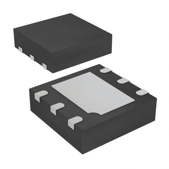
| 描述 | IC TEMP SENSOR DGTL I2C 8MSOP板上安装温度传感器 Silicon temp sensor with I2C interface |
| 产品分类 | |
| 品牌 | Microchip Technology |
| 产品手册 | |
| 产品图片 |
|
| rohs | 符合RoHS无铅 / 符合限制有害物质指令(RoHS)规范要求 |
| 产品系列 | 板上安装温度传感器,Microchip Technology MCP9808-E/MS- |
| 数据手册 | http://www.microchip.com/mymicrochip/filehandler.aspx?ddocname=en556196 |
| 产品型号 | MCP9808-E/MS |
| 产品种类 | 板上安装温度传感器 |
| 传感器类型 | 内部 |
| 供应商器件封装 | 8-MSOP |
| 关闭 | Shutdown |
| 其它名称 | MCP9808EMS |
| 准确性 | +/- 1 C |
| 功能 | 温度监控系统(传感器) |
| 包装 | 管件 |
| 商标 | Microchip Technology |
| 安装类型 | 表面贴装 |
| 安装风格 | SMD/SMT |
| 封装 | Tube |
| 封装/外壳 | 8-TSSOP,8-MSOP(0.118",3.00mm 宽) |
| 封装/箱体 | MSOP-8 |
| 工作温度 | -40°C ~ 125°C |
| 工厂包装数量 | 100 |
| 感应温度 | -40°C ~ 125°C |
| 拓扑 | ADC(三角积分型),寄存器库 |
| 数字输出-总线接口 | 2-Wire, I2C, SMBus |
| 最大工作温度 | + 125 C |
| 最小工作温度 | - 40 C |
| 标准包装 | 100 |
| 电压-电源 | 2.7 V ~ 5.5 V |
| 电源电压-最大 | 5.5 V |
| 电源电压-最小 | 2.7 V |
| 精度 | ±1°C |
| 设备功能 | Temperature Sensor |
| 输出报警 | 是 |
| 输出电流 | 200 uA |
| 输出类型 | 2 线串行, I²C/SMBUS |
| 输出风扇 | 是 |
| 配用 | /product-detail/zh/1782/1528-1032-ND/4990781 |


- 商务部:美国ITC正式对集成电路等产品启动337调查
- 曝三星4nm工艺存在良率问题 高通将骁龙8 Gen1或转产台积电
- 太阳诱电将投资9.5亿元在常州建新厂生产MLCC 预计2023年完工
- 英特尔发布欧洲新工厂建设计划 深化IDM 2.0 战略
- 台积电先进制程称霸业界 有大客户加持明年业绩稳了
- 达到5530亿美元!SIA预计今年全球半导体销售额将创下新高
- 英特尔拟将自动驾驶子公司Mobileye上市 估值或超500亿美元
- 三星加码芯片和SET,合并消费电子和移动部门,撤换高东真等 CEO
- 三星电子宣布重大人事变动 还合并消费电子和移动部门
- 海关总署:前11个月进口集成电路产品价值2.52万亿元 增长14.8%


PDF Datasheet 数据手册内容提取
MCP9808 ±0.5°C Maximum Accuracy Digital Temperature Sensor Features Description • Accuracy: Microchip Technology Inc.’s MCP9808 digital - ±0.25 (typical) from -40°C to +125°C temperature sensor converts temperatures between -20°C and +100°C to a digital word with - ±0.5°C (maximum) from -20°C to 100°C ±0.25°C/±0.5°C (typical/maximum) accuracy. - ±1°C (maximum) from -40°C to +125°C The MCP9808 comes with user-programmable registers • User-Selectable Measurement Resolution: that provide flexibility for temperature sensing - +0.5°C, +0.25°C, +0.125°C, +0.0625°C applications. The registers allow user-selectable • User-Programmable Temperature Limits: settings such as Shutdown or Low-Power modes and - Temperature Window Limit the specification of temperature Alert window limits and - Critical Temperature Limit critical output limits. When the temperature changes • User-Programmable Temperature Alert Output beyond the specified boundary limits, the MCP9808 outputs an Alert signal. The user has the option of setting • Operating Voltage Range: 2.7V to 5.5V the Alert output signal polarity as an active-low or active- • Operating Current: 200µA (typical) high comparator output for thermostat operation, or as a • Shutdown Current: 0.1µA (typical) temperature Alert interrupt output for microprocessor- • 2-wire Interface: I2C™/SMBus Compatible based systems. The Alert output can also be configured • Available Packages: 2x3 DFN-8, MSOP-8 as a critical temperature output only. This sensor has an industry standard 400kHz, 2-wire, Typical Applications SMBus/I2C compatible serial interface, allowing up to eight or sixteen sensors to be controlled with a single • General Purpose serial bus (see Table3-2 for available Address codes). • Industrial Applications These features make the MCP9808 ideal for • Industrial Freezers and Refrigerators sophisticated, multi-zone, temperature-monitoring • Food Processing applications. • Personal Computers and Servers Package Types • PC Peripherals • Consumer Electronics 8-Pin 2x3 DFN* 8-Pin MSOP • Handheld/Portable Devices SDA 1 8 VDD SDA 1 8 VDD Temperature Accuracy SCL 2 EP 7 A0 SCL 2 7 A0 Alert 3 9 6 A1 Alert 3 6 A1 40% TA= -20°C, 25°C, 85°C, 100°C GND 4 5 A2 GND 4 5 A2 V = 3.3V DD 854 units 30% * Includes Exposed Thermal Pad (EP); see Table3-1. s e c n urre 20% c c O 10% 0% 5 4 3 2 1 0 1 2 3 4 5 0. 0. 0. 0. 0. 0. 0. 0. 0. 0. 0. - - - - - Temperature Accuracy (°C) © 2011 Microchip Technology Inc. DS25095A-page 1
MCP9808 Functional Block Diagram Hysteresis Shutdown Critical Trip Lock Alarm Window Lock Clear Alert Alert Status Output Control Critical Alert only Band Gap Alert Polarity Temperature Alert Comp./Int. Sensor Configuration Temperature ΔΣ ADC T Limit UPPER T Limit LOWER +0.5°C T Limit CRITICAL +0.25°C Manufacturer ID +0.125°C +0.0625°C Device ID/Rev Resolution Register Pointer SMBus/Standard I2C™ Interface A0 A1 A2 Alert SDA SCL VDD GND DS25095A-page 2 © 2011 Microchip Technology Inc.
MCP9808 1.0 ELECTRICAL †Notice: Stresses above those listed under “Maximum CHARACTERISTICS ratings” may cause permanent damage to the device. This is a stress rating only and functional operation of the device at those or any other conditions above those Absolute Maximum Ratings † indicated in the operational listings of this specification is not implied. Exposure to maximum rating conditions V .................................................................................. 6.0V DD for extended periods may affect device reliability. Voltage at All Input/Output Pins..............GND – 0.3V to 6.0V Storage Temperature....................................-65°C to +150°C Ambient Temperature with Power Applied....-40°C to +125°C Junction Temperature (T )..........................................+150°C J ESD Protection on All Pins (HBM:MM)................(4kV:400V) Latch-up Current at Each Pin (+25°C)..................... ±200mA TEMPERATURE SENSOR DC CHARACTERISTICS Electrical Specifications: Unless otherwise indicated, V = 2.7V to 5.5V, GND = Ground and DD T = -40°C to +125°C. A Parameters Sym Min Typ Max Unit Conditions Temperature Sensor Accuracy -20°C < T ≤ +100°C T -0.5 ±0.25 +0.5 °C V = 3.3V A ACY DD -40°C < TA ≤ +125°C TACY -1.0 ±0.25 +1.0 °C VDD = 3.3V Temperature Conversion Time 0.5°C/bit t — 30 — ms 33s/sec (typical) CONV 0.25°C/bit — 65 — ms 15s/sec (typical) 0.125°C/bit — 130 — ms 7s/sec (typical) 0.0625°C/bit — 250 — ms 4s/sec (typical) Power Supply Operating Voltage Range V 2.7 — 5.5 V DD Operating Current I — 200 400 µA DD Shutdown Current I — 0.1 2 µA SHDN Power-on Reset (POR) V — 2.2 — V Threshold for falling V POR DD Power Supply Rejection Δ°C/ΔV — -0.1 — °C/V V = 2.7V to 5.5V, T = +25°C DD DD A Alert Output (open-drain output, external pull-up resistor required), see Section5.2.3 “Alert Output Configuration” High-Level Current (leakage) I — — 1 µA V = V (Active-Low, Pull-up Resistor) OH OH DD Low-Level Voltage V — — 0.4 V I = 3mA (Active-Low, Pull-up Resistor) OL OL Thermal Response, from +25°C (air) to +125°C (oil bath) 8L-DFN t — 0.7 — s Time to 63% (+89°C) RES 8L-MSOP — 1.4 — s © 2011 Microchip Technology Inc. DS25095A-page 3
MCP9808 DIGITAL INPUT/OUTPUT PIN CHARACTERISTICS Electrical Specifications: Unless otherwise indicated, V = 2.7V to 5.5V, GND = Ground and DD T = -40°C to +125°C. A Parameters Sym Min Typ Max Units Conditions Serial Input/Output (SCL, SDA, A0, A1, A2) Input High-Level Voltage V 0.7 V — V V IH DD DD Low-Level Voltage V GND — 0.3 V V IL DD Input Current I — — ±5 µA IN Output (SDA) Low-Level Voltage V — — 0.4 V I = 3mA OL OL High-Level Current (leakage) I — — 1 µA V = 5.5V OH OH Low-Level Current I 6 — — mA V = 0.6V OL OL SDA and SCL Inputs Hysteresis V — 0.05 V — V HYST DD Spike Suppression t — — 50 ns SP Capacitance C — 5 — pF IN GRAPHICAL SYMBOL DESCRIPTION OUTPUT INPUT V Voltage V Voltage DD DD V IH VIL VOL I OL Current Current I IN I OH time time TEMPERATURE CHARACTERISTICS Electrical Specifications: Unless otherwise indicated, V = 2.7V to 5.5V and GND = Ground. DD Parameters Sym Min Typ Max Units Conditions Temperature Ranges Specified Temperature Range T -40 — +125 °C (Note1) A Operating Temperature Range T -40 — +125 °C A Storage Temperature Range T -65 — +150 °C A Thermal Package Resistances Thermal Resistance, 8L-DFN θ — 68 — °C/W JA Thermal Resistance, 8L-MSOP θ — 211 — °C/W JA Note 1: Operation in this range must not cause T to exceed Maximum Junction Temperature (+150°C). J DS25095A-page 4 © 2011 Microchip Technology Inc.
MCP9808 SENSOR SERIAL INTERFACE TIMING SPECIFICATIONS Electrical Specifications: Unless otherwise indicated, V = 2.7V to 5.5V, T = -40°C to +125°C, GND = Ground DD A and C = 80pF. (Note1) L Parameters Sym Min Max Units Conditions 2-Wire SMBus/Standard Mode I2C™ Compatible Interface (Note1) Serial Port Clock Frequency f 0 400 kHz (Note2,4) SC Low Clock t 1300 — ns (Note2) LOW High Clock t 600 — ns (Note2) HIGH Rise Time t 20 300 ns R Fall Time t 20 300 ns F Data in Setup Time t 100 — ns (Note3) SU-DI Data In Hold Time t 0 — ns (Note5) HD-DI Data Out Hold Time t 200 900 ns (Note4) HD-DO Start Condition Setup Time t 600 — ns SU-START Start Condition Hold Time t 600 — ns HD-START Stop Condition Setup Time t 600 — ns SU-STOP Bus Free t 1300 — ns B-FREE Time-out t 25 35 ms OUT Bus Capacitive Load C — 400 pf b Note 1: All values referred to V and V levels. IL MAX IH MIN 2: If t > t or t > t , the temperature sensor I2C interface will time-out. A Repeat Start command LOW OUT HIGH OUT is required for communication. 3: This device can be used in a Standard mode I2C bus system, but the requirement, t ≥ 100ns, must SU-DI be met. This device does not stretch the SCL Low time. 4: As a transmitter, the device provides internal minimum delay time, t , to bridge the undefined HD-DO MIN region (min. 200ns) of the falling edge of SCL, t , to avoid unintended generation of Start or Stop F MAX conditions. 5: As a receiver, SDA should not be sampled at the falling edge of SCL. SDA can transition t 0ns after HD-DI SCL toggles Low. TIMING DIAGRAM t HD-START t B-FREE tSU-START tHIGH tLOW tSU-STOP SCL SDA t OUT t , t R F tSU-DI tHD-DI/tHD-DO START Condition Data Transmission STOP Condition © 2011 Microchip Technology Inc. DS25095A-page 5
MCP9808 NOTES: DS25095A-page 6 © 2011 Microchip Technology Inc.
MCP9808 2.0 TYPICAL PERFORMANCE CURVES Note: The graphs and tables provided following this note are a statistical summary based on a limited number of samples and are provided for informational purposes only. The performance characteristics listed herein are not tested or guaranteed. In some graphs or tables, the data presented may be outside the specified operating range (e.g., outside specified power supply range) and therefore outside the warranted range. Note: Unless otherwise indicated, V = 2.7V to 5.5V, GND = Ground, SDA/SCL pulled-up to V and DD DD T = -40°C to +125°C. A 1.0 40% C) V85D4D =u n3i.t3sV at -20°C, 25°C, 85°C, 100°C TVA== - 230.3°CV, 25°C, 85°C, 100°C cy (° 0.5 240 units at -40°C, 125°C 30% 85D4D units a s cur nce e Ac 0.0 urre 20% ur cc at O er -0.5 10% mp +Std. Dev. +3 * Std. Dev. Te -SAtdve. rDaegve. -3 * Std. Dev. -1.0 0% 5 4 3 2 1 0 1 2 3 4 5 -40 -20 0 20 40 60 80 100 120 0. 0. 0. 0. 0. 0. 0. 0. 0. 0. 0. TA(°C) - - -Tem-pera-ture Accuracy (°C) FIGURE 2-1: Temperature Accuracy. FIGURE 2-4: Temperature Accuracy Histogram. 40% 40% T8V2AD7D= =u - n230i.t3°sCV TV85AD9D= =u 8 n35i.°t3CsV 30% 30% Occurrences 1200%% Occurrences 1200%% 0% 0% 5 4 3 2 1 0 1 2 3 4 5 -0. -0. -0. -0. -0. 0. 0. 0. 0. 0. 0. 0.5 0.4 0.3 0.2 0.1 0.0 0.1 0.2 0.3 0.4 0.5 Temperature Accuracy (°C) - - - - - Temperature Accuracy (°C) FIGURE 2-2: Temperature Accuracy FIGURE 2-5: Temperature Accuracy Histogram, T = -20°C. Histogram, T = +85°C. A A 40% 40% TA= 25°C TA= 100°C VDD= 3.3V VDD= 3.3V 875 units 856 units 30% 30% Occurrences 1200%% Occurrences 20% 10% 0% 0% 5 4 3 2 1 0 1 2 3 4 5 0. 0. 0. 0. 0. 0. 0. 0. 0. 0. 0. 5 4 3 2 1 0 1 2 3 4 5 - - -Tem-pera-ture Accuracy (°C) -0. -0. -0. -0. -0. 0. 0. 0. 0. 0. 0. Temperature Accuracy (°C) FIGURE 2-3: Temperature Accuracy FIGURE 2-6: Temperature Accuracy Histogram, T = +25°C. Histogram, T = +100°C. A A © 2011 Microchip Technology Inc. DS25095A-page 7
MCP9808 Note: Unless otherwise indicated, V = 2.7V to 5.5V, GND = Ground, SDA/SCL pulled-up to V and DD DD T = -40°C to +125°C. A 40% 40% TA= -40°C TA= 125°C VDD= 3.3V VDD= 3.3V 240 units 240 units 30% 30% s s e e c c n n urre 20% urre 20% c c c c O O 10% 10% 0% 0% -0.5 -0.4 -0.3Tem-0.2pera-0.1ture0.0 Accu0.1racy0.2 (°C)0.3 0.4 0.5 -0.5 -0.4 -0.3Tem-0.2pera-0.1ture0.0 Accu0.1racy0.2 (°C)0.3 0.4 0.5 FIGURE 2-7: Temperature Accuracy FIGURE 2-10: Temperature Accuracy Histogram, T = -40°C. Histogram, T = +125°C. A A 400 1.00 350 y (°C) VVDDDD== 23..73VV ∆°C/∆VDD = 0.1°C/V ac 0.50 VDD= 5.5V 300 ur A) cc I (µDD220500 ature A 0.00 er -0.50 1 50 mp Te 100 -1.00 -40 -20 0 20 40 60 80 100 120 -40 -20 0 20 40 60 80 100 120 Temperature (°C) Temperature (°C) FIGURE 2-8: Supply Current vs. FIGURE 2-11: Temperature Accuracy vs Temperature. Supply Voltage. 3 1000 2.5 0.0625°C V) ms) 0.125°C V (POR 2 t(CONV 100 00..255°C°C 1.5 1 10 -40 -20 0 20 40 60 80 100 120 -40 -20 0 20 40 60 80 100 120 Temperature (°C) Temperature (°C) FIGURE 2-9: Power-on Reset Threshold FIGURE 2-12: Temperature Conversion Voltage vs. Temperature. Time vs. Temperature. DS25095A-page 8 © 2011 Microchip Technology Inc.
MCP9808 Note: Unless otherwise indicated, V = 2.7V to 5.5V, GND = Ground, SDA/SCL pulled-up to V and DD DD T = -40°C to +125°C. A 0.4 35 ut V (V)OL 0.3 IOL = 3 mA (ms)OUT 30 Outp 0.2 Bus t A & Alert 0.1 SDA VOL Alert VOL 2MBus/IC 25 SD S 0 20 -40 -20 0 20 40 60 80 100 120 -40 -20 0 20 40 60 80 100 120 Temperature (°C) Temperature (°C) FIGURE 2-13: SDA and Alert Output V FIGURE 2-16: SMBus Time-out vs. OL vs. Temperature. Temperature. 2.00 48 VOL = 0.6V 42 1.50 mA) 36 A) A I (OL 2340 (µSHDN 1.00 D I S 18 0.50 12 6 0.00 -40 -20 0 20 40 60 80 100 120 -40 -20 0 20 40 60 80 100 120 Temperature (°C) Temperature (°C ) FIGURE 2-14: SDA I vs. Temperature. FIGURE 2-17: Shutdown Current vs OL Temperature. 120% C) 1.0 e (%) 100% Error (° 0.5 ∆°C/∆VDD, VDD = 3.3V + 150 mVPP (AC) TTAA == 2+52°5C°C espons 6800%% Temp. 0.0 R d Thermal 2400%% MDFSNO-PR8-o8om to +125°C (Oil bath) Normalize --10..05 No decoupling capacitor 0% 101000 1111,0kkk00 111110,0000000kkkk 1111110000000,00000000kkkkk 111111,00MMMMM0,000 -2 0 2 4 6 8 10 12 14 16 Frequency (Hz) Time (s) FIGURE 2-15: Package Thermal FIGURE 2-18: Power Supply Rejection vs. Response. Frequency. © 2011 Microchip Technology Inc. DS25095A-page 9
MCP9808 NOTES: DS25095A-page 10 © 2011 Microchip Technology Inc.
MCP9808 3.0 PIN DESCRIPTION The descriptions of the pins are listed in Table3-1. TABLE 3-1: PIN FUNCTION TABLE DFN MSOP Symbol Pin Function 1 1 SDA Serial Data Line 2 2 SCL Serial Clock Line 3 3 Alert Temperature Alert Output 4 4 GND Ground 5 5 A2 Slave Address 6 6 A1 Slave Address 7 7 A0 Slave Address 8 8 V Power Pin DD 9 — EP Exposed Thermal Pad (EP); must be connected to GND 3.1 Serial Data Line (SDA) 3.5 Address Pins (A0, A1, A2) SDA is a bidirectional input/output pin, used to serially These pins are device address input pins. transmit data to/from the host controller. This pin The address pins correspond to the Least Significant requires a pull-up resistor. (See Section4.0 “Serial bits (LSbs) of the address bits and the Most Significant Communication”.) bits (MSbs): A6, A5, A4, A3. This is illustrated in Table3-2. 3.2 Serial Clock Line (SCL) TABLE 3-2: MCP9808 ADDRESS BYTE The SCL is a clock input pin. All communication and Device Address Code Slave timing is relative to the signal on this pin. The clock is Address generated by the host or master controller on the bus. (See Section4.0 “Serial Communication”.) A6 A5 A4 A3 A2 A1 A0 MCP9808 0 0 1 1 x(1) x x 3.3 Temperature Alert, Open-Drain MCP9808(2) 1 0 0 1 x x x Output (Alert) Note 1: User-selectable address is shown by ‘x’. A2, A1 and A0 must match the The MCP9808 temperature Alert output pin is an open-drain output. The device outputs a signal when the corresponding device pin configuration. ambient temperature goes beyond the user-programmed 2: Contact factory for this address code. temperature limit. (See Section5.2.3 “Alert Output Configuration”). 3.6 Power Pin (V ) DD V is the power pin. The operating voltage range, as 3.4 Ground Pin (GND) DD specified in the DC electrical specification table, is The GND pin is the system ground pin. applied on this pin. 3.7 Exposed Thermal Pad (EP) There is an internal electrical connection between the Exposed Thermal Pad (EP) and the GND pin. The EP may be connected to the system ground on the Printed Circuit Board (PCB). © 2011 Microchip Technology Inc. DS25095A-page 11
MCP9808 NOTES: DS25095A-page 12 © 2011 Microchip Technology Inc.
MCP9808 4.0 SERIAL COMMUNICATION 4.1.1 DATA TRANSFER Data transfers are initiated by a Start condition 4.1 2-Wire Standard Mode I2C™ (START), followed by a 7-bit device address and a Protocol Compatible Interface read/write bit. An Acknowledge (ACK) from the slave confirms the reception of each byte. Each access must The MCP9808 Serial Clock (SCL) input and the be terminated by a Stop condition (STOP). bidirectional Serial Data (SDA) line form a 2-wire bidirectional, Standard mode, I2C compatible Repeated communication is initiated after tB-FREE. communication port (refer to the Digital Input/Output This device does not support sequential register Pin Characteristics and Sensor Serial Interface read/write. Each register needs to be addressed using Timing Specifications tables). the Register Pointer. The following bus protocol has been defined: This device supports the receive protocol. The register can be specified using the pointer for the initial read. TABLE 4-1: MCP9808 SERIAL BUS Each repeated read or receive begins with a Start PROTOCOL DESCRIPTIONS condition and address byte. The MCP9808 retains the previously selected register. Therefore, it outputs data Term Description from the previously specified register (repeated pointer Master The device that controls the serial bus, specification is not necessary). typically a microcontroller. 4.1.2 MASTER/SLAVE Slave The device addressed by the master, such as the MCP9808. The bus is controlled by a master device (typically a Transmitter Device sending data to the bus. microcontroller) that controls the bus access and generates the Start and Stop conditions. The MCP9808 Receiver Device receiving data from the bus. is a slave device and does not control other devices in START A unique signal from the master to the bus. Both master and slave devices can operate as initiate serial interface with a slave. either transmitter or receiver. However, the master STOP A unique signal from the master to device determines which mode is activated. terminate serial interface from a slave. 4.1.3 START/STOP CONDITION Read/Write A read or write to the MCP9808 registers. A high-to-low transition of the SDA line (while SCL is high) is the Start condition. All data transfers must be ACK A receiver Acknowledges (ACK) the preceded by a Start condition from the master. A reception of each byte by polling the bus. low-to-high transition of the SDA line (while SCL is NAK A receiver Not-Acknowledges (NAK) or high) signifies a Stop condition. releases the bus to show End-of-Data (EOD). If a Start or Stop condition is introduced during data transmission, the MCP9808 releases the bus. All data Busy Communication is not possible transfers are ended by a Stop condition from the because the bus is in use. master. Not Busy The bus is in the Idle state; both SDA and SCL remain high. Data Valid SDA must remain stable before SCL becomes high in order for a data bit to be considered valid. During normal data transfers, SDA only changes state while SCL is low. © 2011 Microchip Technology Inc. DS25095A-page 13
MCP9808 4.1.4 ADDRESS BYTE 4.1.5 DATA VALID Following the Start condition, the host must transmit an After the Start condition, each bit of data in the 8-bit address byte to the MCP9808. The address for the transmission needs to be settled for a time specified by MCP9808 temperature sensor is ‘0011,A2,A1,A0’ in tSU-DATA before SCL toggles from low-to-high (see the binary, where the A2, A1 and A0 bits are set externally Sensor Serial Interface Timing Specifications section). by connecting the corresponding pins to VDD ‘1’ or GND ‘0’. The 7-bit address, transmitted in the serial bit stream, 4.1.6 ACKNOWLEDGE (ACK/NAK) must match the selected address for the MCP9808 to Each receiving device, when addressed, must respond with an ACK. Bit 8 in the address byte is a generate an ACK bit after the reception of each byte. read/write bit. Setting this bit to ‘1’ commands a read The master device must generate an extra clock pulse operation, while ‘0’ commands a write operation (see for ACK to be recognized. Figure 4-1). The Acknowledging device pulls down the SDA line for t before the low-to-high transition of SCL from SU-DATA Address Byte the master. SDA also needs to remain pulled down for t after a high-to-low transition of SCL. H-DATA SCL 1 2 3 4 5 6 7 8 9 During read, the master must signal an End-of-Data (EOD) to the slave, by not generating an ACK bit A C (NAK), once the last bit has been clocked out of the SDA 0 0 1 1 A2 A1 A0 K slave. In this case, the slave will leave the data line Start released to enable the master to generate the Stop AdCdordeess ASddlarveess R/W condition. MCP9808 Response 4.1.7 TIME-OUT See Table3-2. If the SCL stays low or high for the time specified by t , the MCP9808 temperature sensor resets the OUT FIGURE 4-1: Device Addressing. serial interface. This dictates the minimum clock speed as outlined in the specification. DS25095A-page 14 © 2011 Microchip Technology Inc.
MCP9808 5.0 FUNCTIONAL DESCRIPTION The MCP9808 temperature sensors consist of a band- gap-type temperature sensor, a Delta-Sigma Analog-to- Digital Converter (ΔΣ ADC), user-programmable registers and a 2-wire SMBus/I2C protocol compatible serial interface. Figure 5-1 shows a block diagram of the register structure. Hysteresis Shutdown Critical Trip Lock Alarm Win. Lock Clear Alert Alert Status Output Control Critical Alert Only Band Gap Alert Polarity Temperature Alert Comp/Int Sensor Configuration Temperature ΔΣ ADC T Limit UPPER T Lim it LOWER +0.5°C T Limit CRITICAL +0.25°C Manufacturer ID +0.125°C +0.0625°C Device ID/Rev Resolution Register Pointer SMBus/Standard I2C™ Interface A0 A1 A2 Alert SDA SCL VDD GND FIGURE 5-1: Functional Block Diagram. © 2011 Microchip Technology Inc. DS25095A-page 15
MCP9808 5.1 Registers Section5.2.3 “Alert Output Configuration”). In addition, the Critical Temperature Limit register is used The MCP9808 has several registers that are to provide an additional critical temperature limit. user-accessible. These registers include the Tempera- The Configuration register provides access to ture register, Configuration register, Temperature Alert configure the MCP9808 device’s various features. Upper Boundary and Lower Boundary Limit registers, These registers are described in further detail in the Critical Temperature Limit register, Manufacturer following sections. Identification register and Device Identification register. The registers are accessed by sending a Register The Temperature register is read-only, used to access Pointer to the MCP9808, using the serial interface. This the ambient temperature data. This register is double- is an 8-bit write-only pointer. However, the four Least buffered and it is updated every t . The Temperature CONV Significant bits are used as pointers and all unused bits Alert Upper Boundary and Lower Boundary Limit (Register Pointer<7:4>) need to be cleared or set to ‘0’. registers are read/write registers. If the ambient Register5-1 describes the pointer or the address of temperature drifts beyond the user-specified limits, the each register. MCP9808 outputs a signal using the Alert pin (refer to REGISTER 5-1: REGISTER POINTER (WRITE-ONLY) W-0 W-0 W-0 W-0 W-0 W-0 W-0 W-0 — — — — Pointer bits bit 7 bit 0 Legend: R = Readable bit W = Writable bit U = Unimplemented bit, read as ‘0’ -n = Value at POR ‘1’ = Bit is set ‘0’ = Bit is cleared x = Bit is unknown bit 7-4 W: Writable bits Write ‘0’. Bits 7-4 must always be cleared or written to ‘0’. This device has additional registers that are reserved for test and calibration. If these registers are accessed, the device may not perform according to the specification. bit 3-0 Pointer bits 0000 = RFU, Reserved for Future Use (Read-Only register) 0001 = Configuration register (CONFIG) 0010 = Alert Temperature Upper Boundary Trip register (TUPPER) 0011 = Alert Temperature Lower Boundary Trip register (TLOWER) 0100 = Critical Temperature Trip register (TCRIT) 0101 = Temperature register (TA) 0110 = Manufacturer ID register 0111 = Device ID/Revision register 1000 = Resolution register 1xxx = Reserved(1) Note 1: Some registers contain calibration codes and should not be accessed. DS25095A-page 16 © 2011 Microchip Technology Inc.
MCP9808 TABLE 5-1: BIT ASSIGNMENT SUMMARY FOR ALL REGISTERS (See Section5.3 “Summary of Power-on Default” for Power-on Defaults) Register Bit Assignment MSB/ Pointer LSB (Hex) 7 6 5 4 3 2 1 0 0x00 MSB 0 0 0 0 0 0 0 0 LSB 0 0 0 1 1 1 1 1 0x01 MSB 0 0 0 0 0 Hysteresis SHDN LSB Crt Loc Win Loc Int Clr Alt Stat Alt Cnt Alt Sel Alt Pol Alt Mod 0x02 MSB 0 0 0 SIGN 27°C 26°C 25°C 24°C LSB 23°C 22°C 21°C 20°C 2-1°C 2-2°C 0 0 0x03 MSB 0 0 0 SIGN 27°C 26°C 25°C 24°C LSB 23°C 22°C 21°C 20°C 2-1°C 2-2°C 0 0 0x04 MSB 0 0 0 SIGN 27°C 26°C 25°C 24°C LSB 23°C 22°C 21°C 20°C 2-1°C 2-2°C 0 0 0x05 MSB T ≥ T T > T T < T SIGN 27°C 26°C 25°C 24°C A CRIT A UPPER A LOWER LSB 23°C 22°C 21°C 20°C 2-1°C 2-2°C 2-3°C 2-4°C 0x06 MSB 0 0 0 0 0 0 0 0 LSB 0 1 0 1 0 1 0 0 0x07 MSB 0 0 0 0 0 1 0 0 LSB 0 0 0 0 0 0 0 0 0x08 LSB 0 0 0 0 0 0 1 1 © 2011 Microchip Technology Inc. DS25095A-page 17
MCP9808 5.1.1 SENSOR CONFIGURATION user-specified temperature boundary (see REGISTER (CONFIG) Section5.2.2 “Temperature Hysteresis (THYST)”. The Continuous Conversion or Shutdown mode is The MCP9808 has a 16-bit Configuration register selected using bit 8. In Shutdown mode, the band gap (CONFIG) that allows the user to set various functions for temperature sensor circuit stops converting a robust temperature monitoring system. Bits 10 through temperature and the Ambient Temperature register 0 are used to select the temperature alert output (T ) holds the previous temperature data (see hysteresis, device shutdown or Low-Power mode, A Section5.2.1 “Shutdown Mode”). Bits 7 and 6 are temperature boundary and critical temperature lock, and used to lock the user-specified boundaries T , temperature Alert output enable/disable. In addition, Alert UPPER T and T to prevent an accidental rewrite. output condition (output set for T and T LOWER CRIT UPPER LOWER The Lock bits are cleared by resetting the power. Bits 5 temperature boundary or T only), Alert output status CRIT through 0 are used to configure the temperature Alert and Alert output polarity and mode (Comparator Output output pin. All functions are described in Register5-2 or Interrupt Output mode) are user-configurable. (see Section5.2.3 “Alert Output Configuration”). The temperature hysteresis bits 10 and 9 can be used to prevent output chatter when the ambient temperature gradually changes beyond the REGISTER 5-2: CONFIG: CONFIGURATION REGISTER (→ ADDRESS ‘0000 0001’b) U-0 U-0 U-0 U-0 U-0 R/W-0 R/W-0 R/W-0 — — — — — T SHDN HYST bit 15 bit 8 R/W-0 R/W-0 R/W-0 R-0 R/W-0 R/W-0 R/W-0 R/W-0 Crit. Lock Win. Lock Int. Clear Alert Stat. Alert Cnt. Alert Sel. Alert Pol. Alert Mod. bit 7 bit 0 Legend: R = Readable bit W = Writable bit U = Unimplemented bit, read as ‘0’ -n = Value at POR ‘1’ = Bit is set ‘0’ = Bit is cleared x = Bit is unknown bit 15-11 Unimplemented: Read as ‘0’ bit 10-9 T : T and T Limit Hysteresis bits HYST UPPER LOWER 00 = 0°C (power-up default) 01 = +1.5°C 10 = +3.0°C 11 = +6.0°C (Refer to Section5.2.3 “Alert Output Configuration”.) This bit can not be altered when either of the Lock bits are set (bit 6 and bit 7). This bit can be programmed in Shutdown mode. bit 8 SHDN: Shutdown Mode bit 0 = Continuous conversion (power-up default) 1 = Shutdown (Low-Power mode) In shutdown, all power-consuming activities are disabled, though all registers can be written to or read. This bit cannot be set to ‘1’ when either of the Lock bits is set (bit 6 and bit 7). However, it can be cleared to ‘0’ for continuous conversion while locked (refer to Section5.2.1 “Shutdown Mode”). DS25095A-page 18 © 2011 Microchip Technology Inc.
MCP9808 REGISTER 5-2: CONFIG: CONFIGURATION REGISTER (→ ADDRESS ‘0000 0001’b) bit 7 Crit. Lock: T Lock bit CRIT 0 = Unlocked. TCRIT register can be written (power-up default) 1 = Locked. TCRIT register can not be written When enabled, this bit remains set to ‘1’ or locked until cleared by an internal Reset (Section5.3 “Summary of Power-on Default”). This bit can be programmed in Shutdown mode. bit 6 Win. Lock: T and T Window Lock bit UPPER LOWER 0 = Unlocked; TUPPER and TLOWER registers can be written (power-up default) 1 = Locked; TUPPER and TLOWER registers can not be written When enabled, this bit remains set to ‘1’ or locked until cleared by a Power-on Reset (Section5.3 “Summary of Power-on Default”). This bit can be programmed in Shutdown mode. bit 5 Int. Clear: Interrupt Clear bit 0 = No effect (power-up default) 1 = Clear interrupt output; when read, this bit returns to ‘0’ This bit can not be set to ‘1’ in Shutdown mode, but it can be cleared after the device enters Shutdown mode. bit 4 Alert Stat.: Alert Output Status bit 0 = Alert output is not asserted by the device (power-up default) 1 = Alert output is asserted as a comparator/Interrupt or critical temperature output This bit can not be set to ‘1’ or cleared to ‘0’ in Shutdown mode. However, if the Alert output is config- ured as Interrupt mode, and if the host controller clears to ‘0’, the interrupt, using bit 5 while the device is in Shutdown mode, then this bit will also be cleared ‘0’. bit 3 Alert Cnt.: Alert Output Control bit 0 = Disabled (power-up default) 1 = Enabled This bit can not be altered when either of the Lock bits are set (bit 6 and bit 7). This bit can be programmed in Shutdown mode, but the Alert output will not assert or deassert. bit 2 Alert Sel.: Alert Output Select bit 0 = Alert output for TUPPER, TLOWER and TCRIT (power-up default) 1 = TA > TCRIT only (TUPPER and TLOWER temperature boundaries are disabled) When the Alarm Window Lock bit is set, this bit cannot be altered until unlocked (bit 6). This bit can be programmed in Shutdown mode, but the Alert output will not assert or deassert. bit 1 Alert Pol.: Alert Output Polarity bit 0 = Active-low (power-up default; pull-up resistor required) 1 = Active-high This bit cannot be altered when either of the Lock bits are set (bit 6 and bit 7). This bit can be programmed in Shutdown mode, but the Alert output will not assert or deassert. bit 0 Alert Mod.: Alert Output Mode bit 0 = Comparator output (power-up default) 1 = Interrupt output This bit cannot be altered when either of the Lock bits are set (bit 6 and bit 7). This bit can be programmed in Shutdown mode, but the Alert output will not assert or deassert. © 2011 Microchip Technology Inc. DS25095A-page 19
MCP9808 Writing to the CONFIG Register to Enable the Event Output Pin <0000 0000 0000 1000>b: 1 2 3 4 5 6 7 8 1 2 3 4 5 6 7 8 SCL A A SDA S 0 0 1 1 A A A W C 0 0 0 0 0 0 0 1 C 2 1 0 K K Address Byte Configuration Pointer MCP9808 MCP9808 1 2 3 4 5 6 7 8 1 2 3 4 5 6 7 8 A A 0 0 0 0 0 0 0 0 C 0 0 0 0 1 0 0 0 C P K K MSB Data LSB Data MCP9808 MCP9808 Note: This is an example routine (see Appendix A: “Source Code”). i2c_start(); // send START command i2c_write(AddressByte & 0xFE); //WRITE Command (see Section4.1.4 “Address Byte”) //also, make sure bit 0 is cleared ‘0’ i2c_write(0x01); // Write CONFIG Register i2c_write(0x00); // Write data i2c_write(0x08); // Write data i2c_stop(); // send STOP command FIGURE 5-2: Timing Diagram for Writing to the Configuration Register (see Section4.0 “Serial Communication”). DS25095A-page 20 © 2011 Microchip Technology Inc.
MCP9808 Reading the CONFIG Register: 1 2 3 4 5 6 7 8 1 2 3 4 5 6 7 8 SCL Note: It is not necessary to select the Register Pointer if it was set A A SDA S 0 0 1 1 A A A W C 0 0 0 0 0 0 0 1 C from the previous 2 1 0 K K read/write. Address Byte Configuration Pointer MCP9808 MCP9808 1 2 3 4 5 6 7 8 1 2 3 4 5 6 7 8 1 2 3 4 5 6 7 8 SCL SDA S 0 0 1 1 A A A R AC 0 0 0 0 0 0 0 0 AC 0 0 0 0 1 0 0 0 NA P 2 1 0 K K K Address Byte MSB Data LSB Data Master Master MCP9808 Note: This is an example routine (see Appendix A: “Source Code”). i2c_start(); // send START command i2c_write(AddressByte & 0xFE); //WRITE Command (see Section4.1.4 “Address Byte”) //also, make sure bit 0 is cleared ‘0’ i2c_write(0x01); // Write CONFIG Register i2c_start(); // send Repeat START command i2c_write(AddressByte | 0x01); //READ Command //also, make sure bit 0 is set ‘1’ UpperByte = i2c_read(ACK); // READ 8 bits //and Send ACK bit LowerByte = i2c_read(NAK); // READ 8 bits //and Send NAK bit i2c_stop(); // send STOP command FIGURE 5-3: Timing Diagram for Reading from the Configuration Register (see Section4.0 “Serial Communication”). © 2011 Microchip Technology Inc. DS25095A-page 21
MCP9808 5.1.2 UPPER/LOWER/CRITICAL the maximum and minimum temperature boundary or TEMPERATURE LIMIT REGISTERS temperature window that can be used to monitor (T /T /T ) ambient temperature. If this feature is enabled UPPER LOWER CRIT (Section5.1.1 “Sensor Configuration Register The MCP9808 has a 16-bit read/write Alert Output (CONFIG)”) and the ambient temperature exceeds the Temperature Upper Boundary register (T ), a 16-bit UPPER specified boundary or window, the MCP9808 asserts an Lower Boundary register (T ) and a 16-bit Critical LOWER Alert output. (Refer to Section5.2.3 “Alert Output Boundary register (T ) that contain 11-bit data in CRIT Configuration”). two’s complement format (0.25°C). This data represents REGISTER 5-3: T /T /T UPPER/LOWER/CRITICAL TEMPERATURE LIMIT REGISTER UPPER LOWER CRIT (→ ADDRESS ‘0000 0010’b/‘0000 0011’b/‘0000 0100’b)(1) U-0 U-0 U-0 R/W-0 R/W-0 R/W-0 R/W-0 R/W-0 — — — Sign 27°C 26°C 25°C 24°C bit 15 bit 8 R/W-0 R/W-0 R/W-0 R/W-0 R/W-0 R/W-0 U-0 U-0 23°C 22°C 21°C 20°C 2-1°C 2-2°C — — bit 7 bit 0 Legend: R = Readable bit W = Writable bit U = Unimplemented bit, read as ‘0’ -n = Value at POR ‘1’ = Bit is set ‘0’ = Bit is cleared x = Bit is unknown bit 15-13 Unimplemented: Read as ‘0’ bit 12 Sign: Sign bit 0 = TA ≥ 0°C 1 = TA < 0°C bit 11-2 T /T /T : Temperature Boundary bits UPPER LOWER CRIT Temperature boundary trip data in two’s complement format. bit 1-0 Unimplemented: Read as ‘0’ Note 1: This table shows two 16-bit registers for TUPPER, TLOWER and TCRIT, located at ‘0000 0010b’, ‘0000 0011b’ and ‘0000 0100b’, respectively. DS25095A-page 22 © 2011 Microchip Technology Inc.
MCP9808 Writing +90°C to the TUPPER Register <0000 0101 1010 0000>b: 1 2 3 4 5 6 7 8 1 2 3 4 5 6 7 8 SCL A A SDA S 0 0 1 1 A A A W C 0 0 0 0 0 0 1 0 C 2 1 0 K K Address Byte T Pointer UPPER MCP9808 MCP9808 1 2 3 4 5 6 7 8 1 2 3 4 5 6 7 8 A A 0 0 0 0 0 1 0 1 C 1 0 1 0 0 0 0 0 C P K K MSB Data LSB Data MCP9808 MCP9808 Reading from the T Register: UPPER 1 2 3 4 5 6 7 8 1 2 3 4 5 6 7 8 SCL Note: It is not necessary to select the Register Pointer if it was set A A SDA S 0 0 1 1 A A A W C 0 0 0 0 0 0 1 0 C from the previous 2 1 0 K K read/write. Address Byte T Pointer UPPER MCP9808 MCP9808 1 2 3 4 5 6 7 8 1 2 3 4 5 6 7 8 1 2 3 4 5 6 7 8 SCL SDA S 0 0 1 1 A A A R AC 0 0 0 0 0 1 0 1 AC 1 0 1 0 0 0 0 0 NA P 2 1 0 K K K Address Byte MSB Data LSB Data MCP9808 Master Master FIGURE 5-4: Timing Diagram for Writing and Reading from the T Register (see Section4.0 UPPER “Serial Communication”). © 2011 Microchip Technology Inc. DS25095A-page 23
MCP9808 5.1.3 AMBIENT TEMPERATURE In addition, the T register uses three bits (T <15:13>) A A REGISTER (T ) to reflect the Alert pin state. This allows the user to A identify the cause of the Alert output trigger (see The MCP9808 uses a band gap temperature sensor Section5.2.3 “Alert Output Configuration”); bit 15 is circuit to output analog voltage proportional to absolute temperature. An internal ΔΣ ADC is used to convert the set to ‘1’ if TA is greater than or equal to TCRIT, bit 14 is analog voltage to a digital word. The digital word is set to ‘1’ if TA is greater than TUPPER and bit 13 is set to loaded to a 16-bit read-only Ambient Temperature ‘1’ if TA is less than TLOWER. register (TA) that contains 13-bit temperature data in The TA register bit assignment and boundary two’s complement format. conditions are described in Register5-4. The T register bits (T <12:0>) are double-buffered. A A Therefore, the user can access the register, while in the background, the MCP9808 performs an Analog-to- Digital conversion. The temperature data from the ΔΣ ADC is loaded in parallel to the T register at t A CONV refresh rate. REGISTER 5-4: T : AMBIENT TEMPERATURE REGISTER (→ ADDRESS ‘0000 0101’b)(1) A R-0 R-0 R-0 R-0 R-0 R-0 R-0 R-0 T vs. T (1) T vs. T (1) T vs. T (1) SIGN 27 °C 26 °C 25 °C 24 °C A CRIT A UPPER A LOWER bit 15 bit 8 R-0 R-0 R-0 R-0 R-0 R-0 R-0 R-0 23 °C 22 °C 21 °C 20 °C 2-1 °C 2-2 °C(2) 2-3 °C(2) 2-4 °C(2) bit 7 bit 0 Legend: R = Readable bit W = Writable bit U = Unimplemented bit, read as ‘0’ -n = Value at POR ‘1’ = Bit is set ‘0’ = Bit is cleared x = Bit is unknown bit 15 T vs. T bit(1) A CRIT 0 =TA < TCRIT 1 =TA ≥ TCRIT bit 14 T vs. T bit(1) A UPPER 0 = TA ≤ TUPPER 1 = TA > TUPPER bit 13 T vs. T bit(1) A LOWER 0 = TA ≥ TLOWER 1 = TA < TLOWER bit 12 SIGN bit 0 = TA ≥ 0°C 1 = TA < 0°C bit 11-0 T : Ambient Temperature bits(2) A 12-bit ambient temperature data in two’s complement format. Note 1: Bits 15, 14 and 13 are not affected by the status of the Alert Output Configuration (CONFIG<5:0> bits, Register5-2). 2: Bits 2, 1 and 0 may remain clear at ‘0’ depending on the status of the Resolution register (Register5-7). The power-up default is 0.25°C/bit; bits 1 and 0 remain clear ‘0’. DS25095A-page 24 © 2011 Microchip Technology Inc.
MCP9808 5.1.3.1 T Bits to Temperature Conversion instruction code, outlined in Example5-1, shows the A communication flow; also see Figure 5-5 for the timing To convert the T bits to decimal temperature, the A diagram. upper three boundary bits (T <15:13>) must be A masked out. Then, determine the SIGN bit (bit 12) to EQUATION 5-1: BYTES TO check positive or negative temperature, shift the bits TEMPERATURE accordingly, and combine the upper and lower bytes of the 16-bit register. The upper byte contains data for CONVERSION temperatures greater than +32°C while the lower byte Temperature T ≥ 0°C contains data for temperature less than +32°C, includ- A 4 –4 T = (UpperByte×2 +LowerByte×2 ) ing fractional data. When combining the upper and A lower bytes, the upper byte must be right-shifted by Temperature < 0°C 4bits (or multiply by 24) and the lower byte must be left- 4 –4 T = 256–(UpperByte×2 +LowerByte×2 ) shifted by 4 bits (or multiply by 2-4). Adding the results A of the shifted values provides the temperature data in Where: decimal format (see Equation5-1). T = Ambient Temperature (°C) A The temperature bits are in two’s compliment format, UpperByte = T bit 15 to bit 8 A therefore, positive temperature data and negative tem- LowerByte = T bit 7 to bit 0 A perature data are computed differently. Equation5-1 shows the temperature computation. The example EXAMPLE 5-1: SAMPLE INSTRUCTION CODE This example routine assumes the variables and I2C™ communication subroutines are predefined (see Appendix A: “Source Code”): i2c_start(); // send START command i2c_write (AddressByte & 0xFE); //WRITE Command (see Section4.1.4 “Address Byte”) //also, make sure bit 0 is cleared ‘0’ i2c_write(0x05); // Write T Register Address A i2c_start(); //Repeat START i2c_write(AddressByte | 0x01); // READ Command (see Section4.1.4 “Address Byte”) //also, make sure bit 0 is Set ‘1’ UpperByte = i2c_read(ACK); // READ 8 bits //and Send ACK bit LowerByte = i2c_read(NAK); // READ 8 bits //and Send NAK bit i2c_stop(); // send STOP command //Convert the temperature data //First Check flag bits if ((UpperByte & 0x80) == 0x80){ //T ³ T A CRIT } if ((UpperByte & 0x40) == 0x40){ //T > T A UPPER } if ((UpperByte & 0x20) == 0x20){ //T < T A LOWER } UpperByte = UpperByte & 0x1F; //Clear flag bits if ((UpperByte & 0x10) == 0x10){ //T < 0°C A UpperByte = UpperByte & 0x0F; //Clear SIGN Temperature = 256 - (UpperByte x 16 + LowerByte / 16); }else //T ³ 0°C A Temperature = (UpperByte x 16 + LowerByte / 16); //Temperature = Ambient Temperature (°C) © 2011 Microchip Technology Inc. DS25095A-page 25
MCP9808 1 2 3 4 5 6 7 8 1 2 3 4 5 6 7 8 SCL Note: It is not necessary to select the Register Pointer if it was set from SDA S 0 0 1 1 A A A W AC 0 0 0 0 0 1 0 1 AC the previous read/write. 2 1 0 K K Address Byte T Pointer A MCP9808 MCP9808 1 2 3 4 5 6 7 8 1 2 3 4 5 6 7 8 1 2 3 4 5 6 7 8 SCL SDA S 0 0 1 1 A A A R AC 0 0 0 0 0 0 0 1 AC 1 0 0 1 0 1 0 0 NA P 2 1 0 K K K Address Byte MSB Data LSB Data MCP9808 Master Master FIGURE 5-5: Timing Diagram for Reading +25.25°C Temperature from the T Register A (see Section4.0 “Serial Communication”). DS25095A-page 26 © 2011 Microchip Technology Inc.
MCP9808 5.1.4 MANUFACTURER ID REGISTER This register is used to identify the manufacturer of the device in order to perform manufacturer-specific operation. The Manufacturer ID for the MCP9808 is 0x0054 (hexadecimal). REGISTER 5-5: MANUFACTURER ID REGISTER – READ-ONLY (→ ADDRESS ‘0000 0110’b) R-0 R-0 R-0 R-0 R-0 R-0 R-0 R-0 Manufacturer ID bit 15 bit 8 R-0 R-1 R-0 R-1 R-0 R-1 R-0 R-0 Manufacturer ID bit 7 bit 0 Legend: R = Readable bit W = Writable bit U = Unimplemented bit, read as ‘0’ -n = Value at POR ‘1’ = Bit is set ‘0’ = Bit is cleared x = Bit is unknown bit 15-0 Device Manufacturer Identification bits 1 2 3 4 5 6 7 8 1 2 3 4 5 6 7 8 Note: It is not necessary to SCL select the Register Pointer if it was set A A from the previous SDA S 0 0 1 1 A2 A1 A0 W CK 0 0 0 0 0 1 1 0 CK read/write. Address Byte Manufacturer ID Pointer MCP9808 MCP9808 1 2 3 4 5 6 7 8 1 2 3 4 5 6 7 8 1 2 3 4 5 6 7 8 SCL SDA S 0 0 1 1 A A A R AC 0 0 0 0 0 0 0 0 AC 0 1 0 1 0 1 0 0 NA P 2 1 0 K K K Address Byte MSB Data LSB Data MCP9808 Master Master FIGURE 5-6: Timing Diagram for Reading the Manufacturer ID Register (see Section4.0 “Serial Communication”). © 2011 Microchip Technology Inc. DS25095A-page 27
MCP9808 5.1.5 DEVICE ID AND REVISION REGISTER The upper byte of this register is used to specify the device identification and the lower byte is used to specify the device revision. The Device ID for the MCP9808 is 0x04 (hex). The revision begins with 0x00 (hex) for the first release, with the number being incremented as revised versions are released. REGISTER 5-6: DEVICE ID AND DEVICE REVISION – READ-ONLY (→ ADDRESS ‘0000 0111’b) R-0 R-0 R-0 R-0 R-0 R-1 R-0 R-0 Device ID bit 15 bit 8 R-0 R-0 R-0 R-0 R-0 R-0 R-0 R-0 Device Revision bit 7 bit 0 Legend: R = Readable bit W = Writable bit U = Unimplemented bit, read as ‘0’ -n = Value at POR ‘1’ = Bit is set ‘0’ = Bit is cleared x = Bit is unknown bit 15-8 Device ID: Bit 15 to bit 8 are used for device ID bit 7-0 Device Revision: Bit 7 to bit 0 are used for device revision 1 2 3 4 5 6 7 8 1 2 3 4 5 6 7 8 Note: It is not necessary to SCL select the Register Pointer if it was set SDA S 0 0 1 1 A A A W AC 0 0 0 0 0 1 1 1 AC from the previous 2 1 0 K K read/write. Address Byte Device ID Pointer MCP9808 MCP9808 1 2 3 4 5 6 7 8 1 2 3 4 5 6 7 8 1 2 3 4 5 6 7 8 SCL SDA S 0 0 1 1 A A A R AC 0 0 0 0 0 1 0 0 AC 0 0 0 0 0 0 0 0 NA P 2 1 0 K K K Address Byte MSB Data LSB Data Master Master MCP9808 FIGURE 5-7: Timing Diagram for Reading Device ID and Device Revision Register (see Section4.0 “Serial Communication”). DS25095A-page 28 © 2011 Microchip Technology Inc.
MCP9808 5.1.6 RESOLUTION REGISTER This register allows the user to change the sensor resolution (see Section5.2.4 “Temperature Resolution”). The POR default resolution is +0.0625°C. The selected resolution is also reflected in the Capability register (see Register5-2). REGISTER 5-7: RESOLUTION REGISTER (→ ADDRESS ‘0000 1000’b) U-0 U-0 U-0 U-0 U-0 U-0 R/W-1 R/W-1 — — — — — — Resolution bit 7 bit 0 Legend: R = Readable bit W = Writable bit U = Unimplemented bit, read as ‘0’ -n = Value at POR ‘1’ = Bit is set ‘0’ = Bit is cleared x = Bit is unknown bit 7-2 Unimplemented: Read as ‘0’ bit 1-0 Resolution bits 00 = +0.5°C (tCONV = 30ms typical) 01 = +0.25°C (tCONV = 65ms typical) 10 = +0.125°C (tCONV = 130ms typical) 11 = +0.0625°C (power-up default, tCONV = 250ms typical) 1 2 3 4 5 6 7 8 1 2 3 4 5 6 7 8 1 2 3 4 5 6 7 8 SCL SDA S 0 0 1 1 A A A W AC 0 0 0 0 1 0 0 0 AC 0 0 0 0 0 0 1 1 AC P 2 1 0 K K K Address Byte Resolution Pointer Data MCP9808 MCP9808 MCP9808 FIGURE 5-8: Timing Diagram for Changing T Resolution to +0.0625°C <0000 0011>b (see A Section4.0 “Serial Communication”). © 2011 Microchip Technology Inc. DS25095A-page 29
MCP9808 5.2 SENSOR FEATURE DESCRIPTION V 5.2.1 SHUTDOWN MODE DD MCP9808 Shutdown mode disables all power consuming R activities (including temperature sampling operations) PU while leaving the serial interface active. This mode is selected by setting bit 8 of CONFIG to ‘1’. In this mode, Alert Output the device consumes I . It remains in this mode SHDN until bit 8 is cleared to ‘0’ to enable Continuous Conversion mode or until power is recycled. The Shutdown bit (bit 8) cannot be set to ‘1’ while the FIGURE 5-9: Active-Low Alert Output CONFIG<7:6> bits (Lock bits) are set to ‘1’. However, it Configuration. can be cleared to ‘0’ or returned to Continuous Conversion mode while locked. The status of the Alert output can be read using CONFIG<4> (Alert Output Status bit). This bit can not In Shutdown mode, all registers can be read or written. be set to ‘1’ in Shutdown mode. However, the serial bus activity increases the shutdown Bits 7 and 6 of the CONFIG register can be used to lock current. In addition, if the device is in shutdown while the T , T and T registers. These bits the Alert pin is asserted, the device will retain the active UPPER LOWER CRIT prevent false triggers at the Alert output due to an state during shutdown. This increases the shutdown accidental rewrite to these registers. current due to the additional Alert output current. The Alert output can also be used as a critical temper- 5.2.2 TEMPERATURE HYSTERESIS ature output using bit 2 of CONFIG (Alert Output Select (T ) bit). When this feature is selected, the Alert output HYST becomes a comparator output. In this mode, the A hysteresis of 0°C, +1.5°C, +3°C or +6°C can be interrupt output configuration (Alert Output Mode bit, selected for the T , T and T temperate UPPER LOWER CRIT CONFIG<0>) is ignored. boundaries, using bits 10 and 9 of CONFIG. The hysteresis applies for decreasing temperature only (hot 5.2.3.1 Comparator Mode to cold) or as temperature drifts below the specified limit. Comparator mode is selected using bit 0 of CONFIG. In this mode, the Alert output is asserted as active-high or The Hysteresis bits can not be changed if either of the active-low, using bit 1 of CONFIG. Figure 5-10 shows Lock bits (CONFIG<7:6) are set to ‘1’. the conditions that toggle the Alert output. The T , T and T boundary conditions UPPER LOWER CRIT If the device enters Shutdown mode with asserted Alert are described graphically in Figure 5-10. output, the output remains asserted during Shutdown mode. The device must be operating in Continuous 5.2.3 ALERT OUTPUT CONFIGURATION Conversion mode for t . The T vs. T , CONV A UPPER The Alert output can be enabled by using bit 3 of the T and T boundary conditions need to be LOWER CRIT CONFIG register (Alert Output Control bit) and can be satisfied in order for the Alert output to deassert. configured as either a comparator output or as an Comparator mode is useful for thermostat type Interrupt Output mode using bit 0 of CONFIG (Alert applications, such as turning on a cooling fan or Output Mode bit). The polarity can also be specified as triggering a system shutdown when the temperature active-high or active-low using bit 1 of CONFIG (Alert exceeds a safe operating range. Polarity bit). This is an open-drain output and requires a pull-up resistor. When the ambient temperature increases above the critical temperature limit, the Alert output is forced to a comparator output (regardless of CONFIG<0>). When the temperature drifts below the critical temperature limit minus hysteresis, the Alert output automatically returns to the state specified by CONFIG<0> bit. DS25095A-page 30 © 2011 Microchip Technology Inc.
MCP9808 5.2.3.2 Interrupt Mode 5.2.4 TEMPERATURE RESOLUTION In Interrupt mode, the Alert output is asserted as active- The MCP9808 is capable of providing temperature high or active-low (depending on the polarity data with +0.5°C to +0.0625°C resolution. The resolu- configuration) when T drifts above or below T tion can be selected using the Resolution register A UPPER and TLOWER limits. The output is deasserted by setting (Register5-7). It is located at address, ‘00001000’b, bit 5 (Interrupt Clear bit) of CONFIG. Shutting down the and it provides measurement flexibility. A +0.0625°C device will not reset or deassert the Alert output. This resolution is set as a POR default by the factory. mode can not be selected when the Alert output is used TABLE 5-2: TEMPERATURE as a critical temperature output only, using bit 2 of CONFIG. CONVERSION TIME This mode is designed for interrupt driven Resolution tCONV Samples/sec microcontroller-based systems. The microcontroller (ms) (typical) receiving the interrupt will have to Acknowledge the +0.5°C 30 33 interrupt by setting bit 5 of the CONFIG register from the +0.25°C 65 15 MCP9808. +0.125°C 130 7 +0.0625°C 250 4 (Power-up Default) © 2011 Microchip Technology Inc. DS25095A-page 31
MCP9808 T – T CRIT HYST T CRIT T – T UPPER HYST T – T UPPER HYST T UPPER T A T – T LOWER HYST T LOWER T – T LOWER HYST Comparator utw) po utL Interrupt Oe- ert ctiv S/w Int. Clear AlA ( Critical Only Comparator uth) pg utHi Interrupt Oe- ert ctiv S/w Int. Clear AlA ( Critical Only Notes: 1 2 1 3 4 3 5 6 7 4 2 Comparator Interrupt Critical T Bits Alert Output Boundary A Notes Conditions Alert Output (Active-Low/High) 15 14 13 1 TA ≥ TLOWER High/Low Low/High High/Low 0 0 0 2 TA < TLOWER – THYST Low/High Low/High High/Low 0 0 1 3 TA > TUPPER Low/High Low/High High/Low 0 1 0 4 TA ≤ TUPPER – THYST High/Low Low/High High/Low 0 0 0 5 TA ≥ TCRIT Low/High Low/High Low/High 1 1 0 6 When T ≥ T , the Alert output is forced to Comparator mode and the CONFIG<0> (Alert Output A CRIT Mode bit) is ignored until T < T – T . In the Interrupt mode, if the interrupt is not cleared A CRIT HYST (bit5 of CONFIG), as shown in the diagram at Note6, then Alert will remain asserted at Note7 until the interrupt is cleared by the controller. 7 TA < TCRIT – THYST Low/High High/Low High/Low 0 1 0 FIGURE 5-10: Alert Output Conditions. DS25095A-page 32 © 2011 Microchip Technology Inc.
MCP9808 5.3 Summary of Power-on Default The MCP9808 has an internal Power-on Reset (POR) circuit. If the power supply voltage, V , glitches below DD the V threshold, the device resets the registers to POR the power-on default settings. Table5-3 shows the power-on default summary for the Temperature Sensor registers. TABLE 5-3: POWER-ON RESET DEFAULTS Registers Default Register Power-Up Default Address Data (Hexadecimal) Register Description Register Name (Hexadecimal) 0x01 CONFIG 0x0000 Comparator Mode Active-Low Output Alert and Critical Output Output Disabled Alert Not Asserted Interrupt Cleared Alert Limits Unlocked Critical Limit Unlocked Continuous Conversion 0°C Hysteresis 0x02 T 0x0000 0°C UPPER 0x03 T 0x0000 0°C LOWER 0x04 T 0x0000 0°C CRIT 0x05 T 0x0000 0°C A 0x06 Manufacturer ID 0x0054 0x0054 (hex) 0x07 Device ID/Device Revision 0x0400 0x0400 (hex) 0x08 Resolution 0x03 0x03 (hex) © 2011 Microchip Technology Inc. DS25095A-page 33
MCP9808 NOTES: DS25095A-page 34 © 2011 Microchip Technology Inc.
MCP9808 6.0 APPLICATIONS INFORMATION ature accuracy error of approximately +0.5°C could result from self-heating if the communication pins sink/source the maximum current specified. 6.1 Layout Considerations For example, if the event output is loaded to maximum The MCP9808 does not require any additional I , Equation6-1 can be used to determine the effect OL components besides the master controller in order to of self-heating. measure temperature. However, it is recommended that a decoupling capacitor of 0.1µF to 1µF be used EQUATION 6-1: EFFECT OF between the V and GND pins. A high-frequency DD SELF-HEATING ceramic capacitor is recommended. It is necessary for the capacitor to be located as close as possible to the TΔ=θJA(VDD•IDD+VOL_Alert•IOL_Alert+VOL_SDA•IOL_SDA) power and ground pins of the device in order to provide Where: effective noise protection. T = T – T Δ J A In addition, good PCB layout is key for better thermal T = Junction Temperature J conduction from the PCB temperature to the sensor T = Ambient Temperature die. For good temperature sensitivity, add a ground A layer under the device pins, as shown in Figure 6-1. θJA = Package Thermal Resistance V = Alert and SDA Output V OL_Alert, SDA OL 6.2 Thermal Considerations (0.4V ) max I = Alert and SDA Output I A potential for self-heating errors can exist if the OL_Alert, SDA OL (3mA ) MCP9808 SDA, SCL and Event lines are heavily max loaded with pull-ups (high current). Typically, the self-heating error is negligible because of the relatively At room temperature (T =+25°C) with maximum A small current consumption of the MCP9808. A temper- I =500µA and V =3.6V, the self-heating due to DD DD power dissipation T is +0.2°C for the DFN-8 package Δ and +0.5°C for the TSSOP-8 package. SDA VDD SCL A0 EP9 Alert A1 GND A2 FIGURE 6-1: DFN Package Layout (Top View). © 2011 Microchip Technology Inc. DS25095A-page 35
MCP9808 NOTES: DS25095A-page 36 © 2011 Microchip Technology Inc.
MCP9808 7.0 PACKAGING INFORMATION 7.1 Package Marking Information 8-Lead DFN (2x3x0.9 mm) Example ALP 141 25 8-Lead MSOP (3x3 mm) Example 9808E 141256 Legend: XX...X Customer-specific information Y Year code (last digit of calendar year) YY Year code (last 2 digits of calendar year) WW Week code (week of January 1 is week ‘01’) NNN Alphanumeric traceability code e3 Pb-free JEDEC designator for Matte Tin (Sn) * This package is Pb-free. The Pb-free JEDEC designator ( e 3 ) can be found on the outer packaging for this package. Note: In the event the full Microchip part number cannot be marked on one line, it will be carried over to the next line, thus limiting the number of available characters for customer-specific information. © 2011 Microchip Technology Inc. DS25095A-page 37
MCP9808 (cid:2)(cid:3)(cid:4)(cid:5)(cid:6)(cid:7)(cid:8)(cid:9)(cid:10)(cid:6)(cid:11)(cid:12)(cid:13)(cid:14)(cid:8)(cid:15)(cid:16)(cid:6)(cid:10)(cid:8)(cid:17)(cid:10)(cid:6)(cid:12)(cid:18)(cid:8)(cid:19)(cid:20)(cid:8)(cid:4)(cid:5)(cid:6)(cid:7)(cid:8)(cid:9)(cid:6)(cid:14)(cid:21)(cid:6)(cid:22)(cid:5)(cid:8)(cid:23)(cid:24)(cid:25)(cid:26)(cid:8)(cid:27)(cid:8)(cid:28)(cid:29)(cid:30)(cid:29)(cid:31) !(cid:8)""(cid:8)#(cid:20)(cid:7)$(cid:8)%(cid:15)(cid:17)(cid:19)& (cid:19)(cid:20)(cid:12)(cid:5)’ 2(cid:21)(cid:20)(cid:14)%(cid:22)(cid:13)(cid:14)&(cid:21) %(cid:14)(cid:19)!(cid:20)(cid:20)(cid:13)(cid:24)%(cid:14)(cid:10)(cid:11)(cid:19)*(cid:11)(cid:12)(cid:13)(cid:14)"(cid:20)(cid:11))(cid:18)(cid:24)(cid:12) ’(cid:14)(cid:10)(cid:25)(cid:13)(cid:11) (cid:13)(cid:14) (cid:13)(cid:13)(cid:14)%(cid:22)(cid:13)(cid:14)(cid:17)(cid:18)(cid:19)(cid:20)(cid:21)(cid:19)(cid:22)(cid:18)(cid:10)(cid:14)(cid:30)(cid:11)(cid:19)*(cid:11)(cid:12)(cid:18)(cid:24)(cid:12)(cid:14)(cid:3)(cid:10)(cid:13)(cid:19)(cid:18)$(cid:18)(cid:19)(cid:11)%(cid:18)(cid:21)(cid:24)(cid:14)(cid:25)(cid:21)(cid:19)(cid:11)%(cid:13)"(cid:14)(cid:11)%(cid:14) (cid:22)%%(cid:10)133)))(cid:28)&(cid:18)(cid:19)(cid:20)(cid:21)(cid:19)(cid:22)(cid:18)(cid:10)(cid:28)(cid:19)(cid:21)&3(cid:10)(cid:11)(cid:19)*(cid:11)(cid:12)(cid:18)(cid:24)(cid:12) D e b N N L K E E2 EXPOSEDPAD NOTE1 NOTE1 1 2 2 1 D2 TOPVIEW BOTTOMVIEW A NOTE2 A3 A1 4(cid:24)(cid:18)% (cid:17)(cid:27)55(cid:27)(cid:17),(cid:23),(cid:8)(cid:3) (cid:2)(cid:18)&(cid:13)(cid:24) (cid:18)(cid:21)(cid:24)(cid:14)5(cid:18)&(cid:18)% (cid:17)(cid:27)6 67(cid:17) (cid:17)(cid:7)8 6!&((cid:13)(cid:20)(cid:14)(cid:21)$(cid:14)(cid:30)(cid:18)(cid:24) 6 9 (cid:30)(cid:18)%(cid:19)(cid:22) (cid:13) (cid:4)(cid:28).(cid:4)(cid:14)/(cid:3)0 7(cid:31)(cid:13)(cid:20)(cid:11)(cid:25)(cid:25)(cid:14):(cid:13)(cid:18)(cid:12)(cid:22)% (cid:7) (cid:4)(cid:28)9(cid:4) (cid:4)(cid:28)(cid:6)(cid:4) (cid:29)(cid:28)(cid:4)(cid:4) (cid:3)%(cid:11)(cid:24)"(cid:21)$$(cid:14) (cid:7)(cid:29) (cid:4)(cid:28)(cid:4)(cid:4) (cid:4)(cid:28)(cid:4)(cid:15) (cid:4)(cid:28)(cid:4). 0(cid:21)(cid:24)%(cid:11)(cid:19)%(cid:14)(cid:23)(cid:22)(cid:18)(cid:19)*(cid:24)(cid:13) (cid:7)+ (cid:4)(cid:28)(cid:15)(cid:4)(cid:14)(cid:8),2 7(cid:31)(cid:13)(cid:20)(cid:11)(cid:25)(cid:25)(cid:14)5(cid:13)(cid:24)(cid:12)%(cid:22) (cid:2) (cid:15)(cid:28)(cid:4)(cid:4)(cid:14)/(cid:3)0 7(cid:31)(cid:13)(cid:20)(cid:11)(cid:25)(cid:25)(cid:14);(cid:18)"%(cid:22) , +(cid:28)(cid:4)(cid:4)(cid:14)/(cid:3)0 ,#(cid:10)(cid:21) (cid:13)"(cid:14)(cid:30)(cid:11)"(cid:14)5(cid:13)(cid:24)(cid:12)%(cid:22) (cid:2)(cid:15) (cid:29)(cid:28)+(cid:4) < (cid:29)(cid:28).. ,#(cid:10)(cid:21) (cid:13)"(cid:14)(cid:30)(cid:11)"(cid:14);(cid:18)"%(cid:22) ,(cid:15) (cid:29)(cid:28).(cid:4) < (cid:29)(cid:28)(cid:16). 0(cid:21)(cid:24)%(cid:11)(cid:19)%(cid:14);(cid:18)"%(cid:22) ( (cid:4)(cid:28)(cid:15)(cid:4) (cid:4)(cid:28)(cid:15). (cid:4)(cid:28)+(cid:4) 0(cid:21)(cid:24)%(cid:11)(cid:19)%(cid:14)5(cid:13)(cid:24)(cid:12)%(cid:22) 5 (cid:4)(cid:28)+(cid:4) (cid:4)(cid:28)(cid:5)(cid:4) (cid:4)(cid:28).(cid:4) 0(cid:21)(cid:24)%(cid:11)(cid:19)%(cid:9)%(cid:21)(cid:9),#(cid:10)(cid:21) (cid:13)"(cid:14)(cid:30)(cid:11)" = (cid:4)(cid:28)(cid:15)(cid:4) < < (cid:19)(cid:20)(cid:12)(cid:5)(cid:11)’ (cid:29)(cid:28) (cid:30)(cid:18)(cid:24)(cid:14)(cid:29)(cid:14)(cid:31)(cid:18) !(cid:11)(cid:25)(cid:14)(cid:18)(cid:24)"(cid:13)#(cid:14)$(cid:13)(cid:11)%!(cid:20)(cid:13)(cid:14)&(cid:11)(cid:26)(cid:14)(cid:31)(cid:11)(cid:20)(cid:26)’(cid:14)(!%(cid:14)&! %(cid:14)((cid:13)(cid:14)(cid:25)(cid:21)(cid:19)(cid:11)%(cid:13)"(cid:14))(cid:18)%(cid:22)(cid:18)(cid:24)(cid:14)%(cid:22)(cid:13)(cid:14)(cid:22)(cid:11)%(cid:19)(cid:22)(cid:13)"(cid:14)(cid:11)(cid:20)(cid:13)(cid:11)(cid:28) (cid:15)(cid:28) (cid:30)(cid:11)(cid:19)*(cid:11)(cid:12)(cid:13)(cid:14)&(cid:11)(cid:26)(cid:14)(cid:22)(cid:11)(cid:31)(cid:13)(cid:14)(cid:21)(cid:24)(cid:13)(cid:14)(cid:21)(cid:20)(cid:14)&(cid:21)(cid:20)(cid:13)(cid:14)(cid:13)#(cid:10)(cid:21) (cid:13)"(cid:14)%(cid:18)(cid:13)(cid:14)((cid:11)(cid:20) (cid:14)(cid:11)%(cid:14)(cid:13)(cid:24)" (cid:28) +(cid:28) (cid:30)(cid:11)(cid:19)*(cid:11)(cid:12)(cid:13)(cid:14)(cid:18) (cid:14) (cid:11))(cid:14) (cid:18)(cid:24)(cid:12)!(cid:25)(cid:11)%(cid:13)"(cid:28) (cid:5)(cid:28) (cid:2)(cid:18)&(cid:13)(cid:24) (cid:18)(cid:21)(cid:24)(cid:18)(cid:24)(cid:12)(cid:14)(cid:11)(cid:24)"(cid:14)%(cid:21)(cid:25)(cid:13)(cid:20)(cid:11)(cid:24)(cid:19)(cid:18)(cid:24)(cid:12)(cid:14)(cid:10)(cid:13)(cid:20)(cid:14)(cid:7)(cid:3)(cid:17),(cid:14)-(cid:29)(cid:5)(cid:28).(cid:17)(cid:28) /(cid:3)01 /(cid:11) (cid:18)(cid:19)(cid:14)(cid:2)(cid:18)&(cid:13)(cid:24) (cid:18)(cid:21)(cid:24)(cid:28)(cid:14)(cid:23)(cid:22)(cid:13)(cid:21)(cid:20)(cid:13)%(cid:18)(cid:19)(cid:11)(cid:25)(cid:25)(cid:26)(cid:14)(cid:13)#(cid:11)(cid:19)%(cid:14)(cid:31)(cid:11)(cid:25)!(cid:13)(cid:14) (cid:22)(cid:21))(cid:24)(cid:14))(cid:18)%(cid:22)(cid:21)!%(cid:14)%(cid:21)(cid:25)(cid:13)(cid:20)(cid:11)(cid:24)(cid:19)(cid:13) (cid:28) (cid:8),21 (cid:8)(cid:13)$(cid:13)(cid:20)(cid:13)(cid:24)(cid:19)(cid:13)(cid:14)(cid:2)(cid:18)&(cid:13)(cid:24) (cid:18)(cid:21)(cid:24)’(cid:14)! !(cid:11)(cid:25)(cid:25)(cid:26)(cid:14))(cid:18)%(cid:22)(cid:21)!%(cid:14)%(cid:21)(cid:25)(cid:13)(cid:20)(cid:11)(cid:24)(cid:19)(cid:13)’(cid:14)$(cid:21)(cid:20)(cid:14)(cid:18)(cid:24)$(cid:21)(cid:20)&(cid:11)%(cid:18)(cid:21)(cid:24)(cid:14)(cid:10)!(cid:20)(cid:10)(cid:21) (cid:13) (cid:14)(cid:21)(cid:24)(cid:25)(cid:26)(cid:28) (cid:17)(cid:18)(cid:19)(cid:20)(cid:21)(cid:19)(cid:22)(cid:18)(cid:10)(cid:23)(cid:13)(cid:19)(cid:22)(cid:24)(cid:21)(cid:25)(cid:21)(cid:12)(cid:26)(cid:2)(cid:20)(cid:11))(cid:18)(cid:24)(cid:12)0(cid:4)(cid:5)(cid:9)(cid:29)(cid:15)+0 DS25095A-page 38 © 2011 Microchip Technology Inc.
MCP9808 Note: For the most current package drawings, please see the Microchip Packaging Specification located at http://www.microchip.com/packaging © 2011 Microchip Technology Inc. DS25095A-page 39
MCP9808 (cid:2)(cid:3)(cid:4)(cid:5)(cid:6)(cid:7)(cid:8)(cid:9)(cid:10)(cid:6)(cid:11)(cid:12)(cid:13)(cid:14)(cid:8)(cid:24)(cid:13)(cid:14)((cid:20)(cid:8))"(cid:6)(cid:10)(cid:10)(cid:8)*(cid:16)(cid:12)(cid:10)(cid:13)+(cid:5)(cid:8)(cid:9)(cid:6)(cid:14)(cid:21)(cid:6)(cid:22)(cid:5)(cid:8)(cid:23)(cid:24))(cid:26)(cid:8)%(cid:24))*(cid:9)& (cid:19)(cid:20)(cid:12)(cid:5)’ 2(cid:21)(cid:20)(cid:14)%(cid:22)(cid:13)(cid:14)&(cid:21) %(cid:14)(cid:19)!(cid:20)(cid:20)(cid:13)(cid:24)%(cid:14)(cid:10)(cid:11)(cid:19)*(cid:11)(cid:12)(cid:13)(cid:14)"(cid:20)(cid:11))(cid:18)(cid:24)(cid:12) ’(cid:14)(cid:10)(cid:25)(cid:13)(cid:11) (cid:13)(cid:14) (cid:13)(cid:13)(cid:14)%(cid:22)(cid:13)(cid:14)(cid:17)(cid:18)(cid:19)(cid:20)(cid:21)(cid:19)(cid:22)(cid:18)(cid:10)(cid:14)(cid:30)(cid:11)(cid:19)*(cid:11)(cid:12)(cid:18)(cid:24)(cid:12)(cid:14)(cid:3)(cid:10)(cid:13)(cid:19)(cid:18)$(cid:18)(cid:19)(cid:11)%(cid:18)(cid:21)(cid:24)(cid:14)(cid:25)(cid:21)(cid:19)(cid:11)%(cid:13)"(cid:14)(cid:11)%(cid:14) (cid:22)%%(cid:10)133)))(cid:28)&(cid:18)(cid:19)(cid:20)(cid:21)(cid:19)(cid:22)(cid:18)(cid:10)(cid:28)(cid:19)(cid:21)&3(cid:10)(cid:11)(cid:19)*(cid:11)(cid:12)(cid:18)(cid:24)(cid:12) D N E E1 NOTE1 1 2 e b c φ A A2 A1 L1 L 4(cid:24)(cid:18)% (cid:17)(cid:27)55(cid:27)(cid:17),(cid:23),(cid:8)(cid:3) (cid:2)(cid:18)&(cid:13)(cid:24) (cid:18)(cid:21)(cid:24)(cid:14)5(cid:18)&(cid:18)% (cid:17)(cid:27)6 67(cid:17) (cid:17)(cid:7)8 6!&((cid:13)(cid:20)(cid:14)(cid:21)$(cid:14)(cid:30)(cid:18)(cid:24) 6 9 (cid:30)(cid:18)%(cid:19)(cid:22) (cid:13) (cid:4)(cid:28)>.(cid:14)/(cid:3)0 7(cid:31)(cid:13)(cid:20)(cid:11)(cid:25)(cid:25)(cid:14):(cid:13)(cid:18)(cid:12)(cid:22)% (cid:7) < < (cid:29)(cid:28)(cid:29)(cid:4) (cid:17)(cid:21)(cid:25)"(cid:13)"(cid:14)(cid:30)(cid:11)(cid:19)*(cid:11)(cid:12)(cid:13)(cid:14)(cid:23)(cid:22)(cid:18)(cid:19)*(cid:24)(cid:13) (cid:7)(cid:15) (cid:4)(cid:28)(cid:16). (cid:4)(cid:28)9. (cid:4)(cid:28)(cid:6). (cid:3)%(cid:11)(cid:24)"(cid:21)$$(cid:14) (cid:7)(cid:29) (cid:4)(cid:28)(cid:4)(cid:4) < (cid:4)(cid:28)(cid:29). 7(cid:31)(cid:13)(cid:20)(cid:11)(cid:25)(cid:25)(cid:14);(cid:18)"%(cid:22) , (cid:5)(cid:28)(cid:6)(cid:4)(cid:14)/(cid:3)0 (cid:17)(cid:21)(cid:25)"(cid:13)"(cid:14)(cid:30)(cid:11)(cid:19)*(cid:11)(cid:12)(cid:13)(cid:14);(cid:18)"%(cid:22) ,(cid:29) +(cid:28)(cid:4)(cid:4)(cid:14)/(cid:3)0 7(cid:31)(cid:13)(cid:20)(cid:11)(cid:25)(cid:25)(cid:14)5(cid:13)(cid:24)(cid:12)%(cid:22) (cid:2) +(cid:28)(cid:4)(cid:4)(cid:14)/(cid:3)0 2(cid:21)(cid:21)%(cid:14)5(cid:13)(cid:24)(cid:12)%(cid:22) 5 (cid:4)(cid:28)(cid:5)(cid:4) (cid:4)(cid:28)>(cid:4) (cid:4)(cid:28)9(cid:4) 2(cid:21)(cid:21)%(cid:10)(cid:20)(cid:18)(cid:24)% 5(cid:29) (cid:4)(cid:28)(cid:6).(cid:14)(cid:8),2 2(cid:21)(cid:21)%(cid:14)(cid:7)(cid:24)(cid:12)(cid:25)(cid:13) (cid:3) (cid:4)? < 9? 5(cid:13)(cid:11)"(cid:14)(cid:23)(cid:22)(cid:18)(cid:19)*(cid:24)(cid:13) (cid:19) (cid:4)(cid:28)(cid:4)9 < (cid:4)(cid:28)(cid:15)+ 5(cid:13)(cid:11)"(cid:14);(cid:18)"%(cid:22) ( (cid:4)(cid:28)(cid:15)(cid:15) < (cid:4)(cid:28)(cid:5)(cid:4) (cid:19)(cid:20)(cid:12)(cid:5)(cid:11)’ (cid:29)(cid:28) (cid:30)(cid:18)(cid:24)(cid:14)(cid:29)(cid:14)(cid:31)(cid:18) !(cid:11)(cid:25)(cid:14)(cid:18)(cid:24)"(cid:13)#(cid:14)$(cid:13)(cid:11)%!(cid:20)(cid:13)(cid:14)&(cid:11)(cid:26)(cid:14)(cid:31)(cid:11)(cid:20)(cid:26)’(cid:14)(!%(cid:14)&! %(cid:14)((cid:13)(cid:14)(cid:25)(cid:21)(cid:19)(cid:11)%(cid:13)"(cid:14))(cid:18)%(cid:22)(cid:18)(cid:24)(cid:14)%(cid:22)(cid:13)(cid:14)(cid:22)(cid:11)%(cid:19)(cid:22)(cid:13)"(cid:14)(cid:11)(cid:20)(cid:13)(cid:11)(cid:28) (cid:15)(cid:28) (cid:2)(cid:18)&(cid:13)(cid:24) (cid:18)(cid:21)(cid:24) (cid:14)(cid:2)(cid:14)(cid:11)(cid:24)"(cid:14),(cid:29)(cid:14)"(cid:21)(cid:14)(cid:24)(cid:21)%(cid:14)(cid:18)(cid:24)(cid:19)(cid:25)!"(cid:13)(cid:14)&(cid:21)(cid:25)"(cid:14)$(cid:25)(cid:11) (cid:22)(cid:14)(cid:21)(cid:20)(cid:14)(cid:10)(cid:20)(cid:21)%(cid:20)! (cid:18)(cid:21)(cid:24) (cid:28)(cid:14)(cid:17)(cid:21)(cid:25)"(cid:14)$(cid:25)(cid:11) (cid:22)(cid:14)(cid:21)(cid:20)(cid:14)(cid:10)(cid:20)(cid:21)%(cid:20)! (cid:18)(cid:21)(cid:24) (cid:14) (cid:22)(cid:11)(cid:25)(cid:25)(cid:14)(cid:24)(cid:21)%(cid:14)(cid:13)#(cid:19)(cid:13)(cid:13)"(cid:14)(cid:4)(cid:28)(cid:29).(cid:14)&&(cid:14)(cid:10)(cid:13)(cid:20)(cid:14) (cid:18)"(cid:13)(cid:28) +(cid:28) (cid:2)(cid:18)&(cid:13)(cid:24) (cid:18)(cid:21)(cid:24)(cid:18)(cid:24)(cid:12)(cid:14)(cid:11)(cid:24)"(cid:14)%(cid:21)(cid:25)(cid:13)(cid:20)(cid:11)(cid:24)(cid:19)(cid:18)(cid:24)(cid:12)(cid:14)(cid:10)(cid:13)(cid:20)(cid:14)(cid:7)(cid:3)(cid:17),(cid:14)-(cid:29)(cid:5)(cid:28).(cid:17)(cid:28) /(cid:3)01 /(cid:11) (cid:18)(cid:19)(cid:14)(cid:2)(cid:18)&(cid:13)(cid:24) (cid:18)(cid:21)(cid:24)(cid:28)(cid:14)(cid:23)(cid:22)(cid:13)(cid:21)(cid:20)(cid:13)%(cid:18)(cid:19)(cid:11)(cid:25)(cid:25)(cid:26)(cid:14)(cid:13)#(cid:11)(cid:19)%(cid:14)(cid:31)(cid:11)(cid:25)!(cid:13)(cid:14) (cid:22)(cid:21))(cid:24)(cid:14))(cid:18)%(cid:22)(cid:21)!%(cid:14)%(cid:21)(cid:25)(cid:13)(cid:20)(cid:11)(cid:24)(cid:19)(cid:13) (cid:28) (cid:8),21 (cid:8)(cid:13)$(cid:13)(cid:20)(cid:13)(cid:24)(cid:19)(cid:13)(cid:14)(cid:2)(cid:18)&(cid:13)(cid:24) (cid:18)(cid:21)(cid:24)’(cid:14)! !(cid:11)(cid:25)(cid:25)(cid:26)(cid:14))(cid:18)%(cid:22)(cid:21)!%(cid:14)%(cid:21)(cid:25)(cid:13)(cid:20)(cid:11)(cid:24)(cid:19)(cid:13)’(cid:14)$(cid:21)(cid:20)(cid:14)(cid:18)(cid:24)$(cid:21)(cid:20)&(cid:11)%(cid:18)(cid:21)(cid:24)(cid:14)(cid:10)!(cid:20)(cid:10)(cid:21) (cid:13) (cid:14)(cid:21)(cid:24)(cid:25)(cid:26)(cid:28) (cid:17)(cid:18)(cid:19)(cid:20)(cid:21)(cid:19)(cid:22)(cid:18)(cid:10)(cid:23)(cid:13)(cid:19)(cid:22)(cid:24)(cid:21)(cid:25)(cid:21)(cid:12)(cid:26)(cid:2)(cid:20)(cid:11))(cid:18)(cid:24)(cid:12)0(cid:4)(cid:5)(cid:9)(cid:29)(cid:29)(cid:29)/ DS25095A-page 40 © 2011 Microchip Technology Inc.
MCP9808 Note: For the most current package drawings, please see the Microchip Packaging Specification located at http://www.microchip.com/packaging © 2011 Microchip Technology Inc. DS25095A-page 41
MCP9808 NOTES: DS25095A-page 42 © 2011 Microchip Technology Inc.
MCP9808 Software License Agreement The software supplied herewith by Microchip Technology Incorporated (the “Company”) is intended and supplied to you, the Company’s customer, for use solely and exclusively with products manufactured by the Company. The software is owned by the Company and/or its supplier, and is protected under applicable copyright laws. All rights are reserved. Any use in violation of the foregoing restrictions may subject the user to criminal sanctions under applicable laws, as well as to civil liability for the breach of the terms and conditions of this license. THIS SOFTWARE IS PROVIDED IN AN “AS IS” CONDITION. NO WARRANTIES, WHETHER EXPRESS, IMPLIED OR STATU- TORY, INCLUDING, BUT NOT LIMITED TO, IMPLIED WARRANTIES OF MERCHANTABILITY AND FITNESS FOR A PARTICU- LAR PURPOSE APPLY TO THIS SOFTWARE. THE COMPANY SHALL NOT, IN ANY CIRCUMSTANCES, BE LIABLE FOR SPECIAL, INCIDENTAL OR CONSEQUENTIAL DAMAGES, FOR ANY REASON WHATSOEVER. APPENDIX A: SOURCE CODE /******************************************************************** FileName: I2C.c Processor: PIC18 Microcontrollers Complier: Microchip C18 (for PIC18) or C30 (for PIC24) Company: Microchip Technology, Inc. #include <p18cxxx.h> // This code is developed for PIC18F2550 //It can be modified to be used with any PICmicro with MSSP module /** PRIVATE PROTOTYPES *********************************************/ void i2c_init(void); void i2c_start(void); void i2c_repStart(void); void i2c_stop(void); unsigned char i2c_write( unsigned char i2cWriteData ); unsigned char i2c_read( unsigned char ack ); /******************************************************************** * Function Name: i2c_init * Return Value: void * Parameters: Enable SSP * Description: This function sets up the SSP1 module on a * PIC18CXXX device for use with a Microchip I2C ********************************************************************/ void i2c_init(void) { TRISBbits.TRISB0 = 1; // Digital Output (make it input only when reading data) TRISBbits.TRISB1 = 1; // Digital Output SSPCON1 = 0x28; // enable I2C Master mode SSPCON2 = 0x00; // clear control bits SSPSTAT = 0x80; // disable slew rate control; disable SMBus SSPADD = 19; // set baud rate to 100 kHz (Fosc = 48 MHz) PIR1bits.SSPIF = 0; PIR2bits.BCLIF = 0; SSPCON2bits.SEN = 0; // force idle condition } © 2011 Microchip Technology Inc. DS25095A-page 45
MCP9808 /******************************************************************** * Function Name: i2c_start * Return Value: void * Parameters: void * Description: Send I2C Start Command ********************************************************************/ void i2c_start(void) { PIR1bits.SSPIF = 0; //clear flag while (SSPSTATbits.BF ); // wait for idle condition SSPCON2bits.SEN = 1; // initiate START condition while (!PIR1bits.SSPIF) ; // wait for a flag to be set PIR1bits.SSPIF = 0; // clear flag } /******************************************************************** * Function Name: i2c_repStart * Return Value: void * Parameters: void * Description: Resend I2C Start Command * ********************************************************************/ void i2c_repStart(void) { PIR1bits.SSPIF = 0; // clear flag while ( SSPSTATbits.BF ) ; // wait for idle condition SSPCON2bits.RSEN = 1; // initiate Repeated START condition while (!PIR1bits.SSPIF) ; // wait for a flag to be set PIR1bits.SSPIF = 0; // clear flag } /******************************************************************** * Function Name: i2c_stop * Return Value: void * Parameters: void * Description: Send I2C Stop command * ********************************************************************/ void i2c_stop(void) { PIR1bits.SSPIF = 0; // clear flag while ( SSPSTATbits.BF ) ; // wait for idle condition SSPCON2bits.PEN = 1; // Initiate STOP condition while (!PIR1bits.SSPIF) ; // wait for a flag to be set PIR1bits.SSPIF = 0; // clear flag } DS25095A-page 46 © 2011 Microchip Technology Inc.
MCP9808 /******************************************************************** * Function Name: i2c_write * Return Value: Status byte for WCOL detection. * Parameters: Single data byte for I2C2 bus. * Description: This routine writes a single byte to the * I2C2 bus. ********************************************************************/ unsigned char i2c_write( unsigned char i2cWriteData ) { PIR1bits.SSPIF = 0; // clear interrupt while ( SSPSTATbits.BF ) ; // wait for idle condition SSPBUF = i2cWriteData; // Load SSPBUF with i2cWriteData (the value to be transmit- ted) while (!PIR1bits.SSPIF) ; // wait for a flag to be set PIR1bits.SSPIF = 0; // clear flag return ( !SSPCON2bits.ACKSTAT ); // function returns '1' if transmission is acknowledged } /******************************************************************** * Function Name: i2c_read * Return Value: contents of SSP2BUF register * Parameters: ack = 1 and nak = 0 * Description: Read a byte from I2C bus and ACK/NAK device ********************************************************************/ unsigned char i2c_read( unsigned char ack ) { unsigned char i2cReadData; PIR1bits.SSPIF = 0;// clear interrupt while ( SSPSTATbits.BF ) ; // wait for idle condition SSPCON2bits.RCEN = 1; // enable receive mode while (!PIR1bits.SSPIF) ; // wait for a flag to be set PIR1bits.SSPIF = 0;// clear flag i2cReadData = SSPBUF; // Read SSPBUF and put it in i2cReadData if ( ack ) { // if ack=1 SSPCON2bits.ACKDT = 0; // then transmit an Acknowledge } else { SSPCON2bits.ACKDT = 1; // otherwise transmit a Not Acknowledge } SSPCON2bits.ACKEN = 1; // send acknowledge sequence while (!PIR1bits.SSPIF) ; // wait for a flag to be set PIR1bits.SSPIF = 0;// clear flag return( i2cReadData ); // return the value read from SSPBUF } © 2011 Microchip Technology Inc. DS25095A-page 47
MCP9808 NOTES: DS25095A-page 48 © 2011 Microchip Technology Inc.
MCP9808 APPENDIX B: REVISION HISTORY Revision A (October 2011) • Original Release of this Document. © 2011 Microchip Technology Inc. DS25095A-page 49
MCP9808 NOTES: DS25095A-page 50 © 2011 Microchip Technology Inc.
MCP9808 PRODUCT IDENTIFICATION SYSTEM To order or obtain information, e.g., on pricing or delivery, refer to the factory or the listed sales office. PART NO. X -X /XX Examples: a) MCP9808-E/MC: Extended Temperature Device Tape and Reel Temperature Package 8LD DFN package. and/or Range Alternate Pinout b) MCP9808-E/MS: Extended Temperature 8LD MSOP package. Device: MCP9808: Digital Temperature Sensor c) MCP9808T-E/MC: Tape and Reel, MCP9808T: Digital Temperature Sensor (Tape and Reel) Extended Temperature 8LD DFN package. Temperature Range: E = -40°C to +125°C d) MCP9808T-E/MS: Tape and Reel, Extended Temperature 8LD MSOP package. Package: MC = Plastic Dual Flat No-Lead (DFN) 2x3, 8-lead MS = Plastic Micro Small Outline (MSOP), 8-lead © 2011 Microchip Technology Inc. DS25095A-page 51
MCP9808 NOTES: DS25095A-page 52 © 2011 Microchip Technology Inc.
Note the following details of the code protection feature on Microchip devices: • Microchip products meet the specification contained in their particular Microchip Data Sheet. • Microchip believes that its family of products is one of the most secure families of its kind on the market today, when used in the intended manner and under normal conditions. • There are dishonest and possibly illegal methods used to breach the code protection feature. All of these methods, to our knowledge, require using the Microchip products in a manner outside the operating specifications contained in Microchip’s Data Sheets. Most likely, the person doing so is engaged in theft of intellectual property. • Microchip is willing to work with the customer who is concerned about the integrity of their code. • Neither Microchip nor any other semiconductor manufacturer can guarantee the security of their code. Code protection does not mean that we are guaranteeing the product as “unbreakable.” Code protection is constantly evolving. We at Microchip are committed to continuously improving the code protection features of our products. Attempts to break Microchip’s code protection feature may be a violation of the Digital Millennium Copyright Act. If such acts allow unauthorized access to your software or other copyrighted work, you may have a right to sue for relief under that Act. Information contained in this publication regarding device Trademarks applications and the like is provided only for your convenience The Microchip name and logo, the Microchip logo, dsPIC, and may be superseded by updates. It is your responsibility to KEELOQ, KEELOQ logo, MPLAB, PIC, PICmicro, PICSTART, ensure that your application meets with your specifications. PIC32 logo, rfPIC and UNI/O are registered trademarks of MICROCHIP MAKES NO REPRESENTATIONS OR Microchip Technology Incorporated in the U.S.A. and other WARRANTIES OF ANY KIND WHETHER EXPRESS OR countries. IMPLIED, WRITTEN OR ORAL, STATUTORY OR OTHERWISE, RELATED TO THE INFORMATION, FilterLab, Hampshire, HI-TECH C, Linear Active Thermistor, INCLUDING BUT NOT LIMITED TO ITS CONDITION, MXDEV, MXLAB, SEEVAL and The Embedded Control QUALITY, PERFORMANCE, MERCHANTABILITY OR Solutions Company are registered trademarks of Microchip FITNESS FOR PURPOSE. Microchip disclaims all liability Technology Incorporated in the U.S.A. arising from this information and its use. Use of Microchip Analog-for-the-Digital Age, Application Maestro, chipKIT, devices in life support and/or safety applications is entirely at chipKIT logo, CodeGuard, dsPICDEM, dsPICDEM.net, the buyer’s risk, and the buyer agrees to defend, indemnify and dsPICworks, dsSPEAK, ECAN, ECONOMONITOR, hold harmless Microchip from any and all damages, claims, FanSense, HI-TIDE, In-Circuit Serial Programming, ICSP, suits, or expenses resulting from such use. No licenses are Mindi, MiWi, MPASM, MPLAB Certified logo, MPLIB, conveyed, implicitly or otherwise, under any Microchip MPLINK, mTouch, Omniscient Code Generation, PICC, intellectual property rights. PICC-18, PICDEM, PICDEM.net, PICkit, PICtail, REAL ICE, rfLAB, Select Mode, Total Endurance, TSHARC, UniWinDriver, WiperLock and ZENA are trademarks of Microchip Technology Incorporated in the U.S.A. and other countries. SQTP is a service mark of Microchip Technology Incorporated in the U.S.A. All other trademarks mentioned herein are property of their respective companies. © 2011, Microchip Technology Incorporated, Printed in the U.S.A., All Rights Reserved. Printed on recycled paper. ISBN: 978-1-61341-739-3 Microchip received ISO/TS-16949:2009 certification for its worldwide headquarters, design and wafer fabrication facilities in Chandler and Tempe, Arizona; Gresham, Oregon and design centers in California and India. The Company’s quality system processes and procedures are for its PIC® MCUs and dsPIC® DSCs, KEELOQ® code hopping devices, Serial EEPROMs, microperipherals, nonvolatile memory and analog products. In addition, Microchip’s quality system for the design and manufacture of development systems is ISO 9001:2000 certified. © 2011 Microchip Technology Inc. DS25095A-page 53
Worldwide Sales and Service AMERICAS ASIA/PACIFIC ASIA/PACIFIC EUROPE Corporate Office Asia Pacific Office India - Bangalore Austria - Wels 2355 West Chandler Blvd. Suites 3707-14, 37th Floor Tel: 91-80-3090-4444 Tel: 43-7242-2244-39 Chandler, AZ 85224-6199 Tower 6, The Gateway Fax: 91-80-3090-4123 Fax: 43-7242-2244-393 Tel: 480-792-7200 Harbour City, Kowloon India - New Delhi Denmark - Copenhagen Fax: 480-792-7277 Hong Kong Tel: 91-11-4160-8631 Tel: 45-4450-2828 Technical Support: Tel: 852-2401-1200 Fax: 91-11-4160-8632 Fax: 45-4485-2829 http://www.microchip.com/ support Fax: 852-2401-3431 India - Pune France - Paris Web Address: Australia - Sydney Tel: 91-20-2566-1512 Tel: 33-1-69-53-63-20 www.microchip.com Tel: 61-2-9868-6733 Fax: 91-20-2566-1513 Fax: 33-1-69-30-90-79 Atlanta Fax: 61-2-9868-6755 Japan - Yokohama Germany - Munich Duluth, GA China - Beijing Tel: 81-45-471- 6166 Tel: 49-89-627-144-0 Tel: 86-10-8569-7000 Fax: 49-89-627-144-44 Tel: 678-957-9614 Fax: 81-45-471-6122 Fax: 678-957-1455 Fax: 86-10-8528-2104 Korea - Daegu Italy - Milan Boston China - Chengdu Tel: 82-53-744-4301 Tel: 39-0331-742611 Westborough, MA Tel: 86-28-8665-5511 Fax: 82-53-744-4302 Fax: 39-0331-466781 Tel: 774-760-0087 Fax: 86-28-8665-7889 Korea - Seoul Netherlands - Drunen Fax: 774-760-0088 China - Chongqing Tel: 82-2-554-7200 Tel: 31-416-690399 Chicago Tel: 86-23-8980-9588 Fax: 82-2-558-5932 or Fax: 31-416-690340 Itasca, IL Fax: 86-23-8980-9500 82-2-558-5934 Spain - Madrid Tel: 630-285-0071 China - Hangzhou Malaysia - Kuala Lumpur Tel: 34-91-708-08-90 Fax: 630-285-0075 Tel: 86-571-2819-3187 Tel: 60-3-6201-9857 Fax: 34-91-708-08-91 Cleveland Fax: 86-571-2819-3189 Fax: 60-3-6201-9859 UK - Wokingham Independence, OH China - Hong Kong SAR Malaysia - Penang Tel: 44-118-921-5869 Tel: 216-447-0464 Tel: 852-2401-1200 Tel: 60-4-227-8870 Fax: 44-118-921-5820 Fax: 216-447-0643 Fax: 852-2401-3431 Fax: 60-4-227-4068 Dallas China - Nanjing Philippines - Manila Addison, TX Tel: 86-25-8473-2460 Tel: 63-2-634-9065 Tel: 972-818-7423 Fax: 86-25-8473-2470 Fax: 63-2-634-9069 Fax: 972-818-2924 China - Qingdao Singapore Detroit Tel: 86-532-8502-7355 Tel: 65-6334-8870 Farmington Hills, MI Fax: 86-532-8502-7205 Fax: 65-6334-8850 Tel: 248-538-2250 Fax: 248-538-2260 China - Shanghai Taiwan - Hsin Chu Tel: 86-21-5407-5533 Tel: 886-3-5778-366 Indianapolis Fax: 86-21-5407-5066 Fax: 886-3-5770-955 Noblesville, IN Tel: 317-773-8323 China - Shenyang Taiwan - Kaohsiung Fax: 317-773-5453 Tel: 86-24-2334-2829 Tel: 886-7-536-4818 Fax: 86-24-2334-2393 Fax: 886-7-330-9305 Los Angeles Mission Viejo, CA China - Shenzhen Taiwan - Taipei Tel: 86-755-8203-2660 Tel: 886-2-2500-6610 Tel: 949-462-9523 Fax: 949-462-9608 Fax: 86-755-8203-1760 Fax: 886-2-2508-0102 China - Wuhan Thailand - Bangkok Santa Clara Santa Clara, CA Tel: 86-27-5980-5300 Tel: 66-2-694-1351 Tel: 408-961-6444 Fax: 86-27-5980-5118 Fax: 66-2-694-1350 Fax: 408-961-6445 China - Xian Tel: 86-29-8833-7252 Toronto Mississauga, Ontario, Fax: 86-29-8833-7256 Canada China - Xiamen Tel: 905-673-0699 Tel: 86-592-2388138 Fax: 905-673-6509 Fax: 86-592-2388130 China - Zhuhai Tel: 86-756-3210040 08/02/11 Fax: 86-756-3210049 DS25095A-page 54 © 2011 Microchip Technology Inc.
Mouser Electronics Authorized Distributor Click to View Pricing, Inventory, Delivery & Lifecycle Information: M icrochip: MCP9808T-E/MC MCP9808T-E/MS MCP9808-E/MS