ICGOO在线商城 > 传感器,变送器 > 温度传感器 - 模拟和数字输出 > TC74A0-5.0VAT
 Datasheet下载
- 型号: TC74A0-5.0VAT
- 制造商: Microchip
- 库位|库存: xxxx|xxxx
- 要求:
| 数量阶梯 | 香港交货 | 国内含税 |
| +xxxx | $xxxx | ¥xxxx |
查看当月历史价格
查看今年历史价格
TC74A0-5.0VAT产品简介:
ICGOO电子元器件商城为您提供TC74A0-5.0VAT由Microchip设计生产,在icgoo商城现货销售,并且可以通过原厂、代理商等渠道进行代购。 TC74A0-5.0VAT价格参考¥13.33-¥19.40。MicrochipTC74A0-5.0VAT封装/规格:温度传感器 - 模拟和数字输出, 温度传感器 数字,本地 -40°C ~ 125°C 7 b TO-220-5。您可以下载TC74A0-5.0VAT参考资料、Datasheet数据手册功能说明书,资料中有TC74A0-5.0VAT 详细功能的应用电路图电压和使用方法及教程。
Microchip Technology的TC74A0-5.0VAT是一款温度传感器,属于温度传感器 - 模拟和数字输出类别。以下是其主要应用场景:

 1. 消费电子设备
   - 应用于笔记本电脑、平板电脑或智能手机等设备中,监控内部温度以防止过热。
   - 在智能家电(如冰箱、空调、微波炉)中,用于精确控制温度并优化能效。

 2. 工业自动化
   - 在工业控制系统中,用于监测电机、变频器或其他发热设备的温度,确保设备运行在安全范围内。
   - 适用于环境监控系统,例如仓库或数据中心的温湿度控制。

 3. 汽车电子
   - 用于车内温度监测,支持空调系统的自动调节功能。
   - 监控电池管理系统(BMS),防止锂电池因过热而损坏。

 4. 医疗设备
   - 在便携式医疗设备(如体温计、血液分析仪)中提供高精度的温度测量。
   - 用于孵化器或冷藏设备中,确保敏感样品或药品存储在合适的温度范围。

 5. 物联网(IoT)
   - 集成到智能家居设备中,例如温控器或智能插座,实现远程温度监控与调节。
   - 在环境监测节点中,与其他传感器配合使用,提供全面的环境数据。

 6. 嵌入式系统
   - 为嵌入式控制器提供实时温度反馈,帮助调整系统性能或触发保护机制。
   - 用于电源模块的热管理,防止过热导致的系统故障。

 特性与优势
- 宽工作电压范围:支持5V供电,兼容多种电源设计。
- 高精度测量:提供准确的温度读数,满足大多数应用需求。
- 简单接口:支持I²C通信协议,便于与微控制器连接。
- 低功耗设计:适合电池供电的便携式设备。

综上所述,TC74A0-5.0VAT凭借其高性能和灵活性,广泛应用于需要精确温度监测的各种场景中。
| 参数 | 数值 |
| 产品目录 | 集成电路 (IC)热管理产品 |
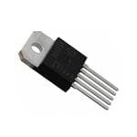
| 描述 | IC DGTL THERM SNSR 5.0V TO220-5板上安装温度传感器 Digital Thermal |
| 产品分类 | |
| 品牌 | Microchip Technology |
| 产品手册 | |
| 产品图片 |
|
| rohs | 符合RoHS无铅 / 符合限制有害物质指令(RoHS)规范要求 |
| 产品系列 | 板上安装温度传感器,Microchip Technology TC74A0-5.0VAT- |
| 数据手册 | http://www.microchip.com/mymicrochip/filehandler.aspx?ddocname=en011621 |
| 产品型号 | TC74A0-5.0VAT |
| 产品目录页面 | |
| 产品种类 | 板上安装温度传感器 |
| 传感器类型 | 内部 |
| 供应商器件封装 | TO-220-5 |
| 关闭 | Shutdown |
| 其它名称 | TC74A05.0VAT |
| 准确性 | +/- 2 C to +/- 3 C |
| 功能 | 温度监控系统(传感器) |
| 包装 | 管件 |
| 商标 | Microchip Technology |
| 安装类型 | 通孔 |
| 安装风格 | Through Hole |
| 封装 | Tube |
| 封装/外壳 | TO-220-5 |
| 封装/箱体 | TO-220-5 |
| 工作温度 | -40°C ~ 125°C |
| 工厂包装数量 | 50 |
| 感应温度 | -40°C ~ 125°C |
| 拓扑 | ADC(三角积分型),寄存器库 |
| 数字输出-位数 | 8 bit |
| 数字输出-总线接口 | 2-Wire, I2C, SMBus |
| 最大工作温度 | + 125 C |
| 最小工作温度 | - 40 C |
| 标准包装 | 50 |
| 电压-电源 | 2.7 V ~ 5.5 V |
| 电源电压-最大 | 5.5 V |
| 电源电压-最小 | 2.7 V |
| 电源电流 | 350 uA |
| 精度 | ±3°C(最大) |
| 设备功能 | Sensor |
| 输出报警 | 无 |
| 输出电流 | 50 mA |
| 输出类型 | Digital |
| 输出风扇 | 无 |
| 配置 | Local |


- 商务部:美国ITC正式对集成电路等产品启动337调查
- 曝三星4nm工艺存在良率问题 高通将骁龙8 Gen1或转产台积电
- 太阳诱电将投资9.5亿元在常州建新厂生产MLCC 预计2023年完工
- 英特尔发布欧洲新工厂建设计划 深化IDM 2.0 战略
- 台积电先进制程称霸业界 有大客户加持明年业绩稳了
- 达到5530亿美元!SIA预计今年全球半导体销售额将创下新高
- 英特尔拟将自动驾驶子公司Mobileye上市 估值或超500亿美元
- 三星加码芯片和SET,合并消费电子和移动部门,撤换高东真等 CEO
- 三星电子宣布重大人事变动 还合并消费电子和移动部门
- 海关总署:前11个月进口集成电路产品价值2.52万亿元 增长14.8%


PDF Datasheet 数据手册内容提取
TC74 Tiny Serial Digital Thermal Sensor Features General Description • Digital Temperature Sensing in SOT-23-5 or The TC74 is a serially accessible, digital temperature TO-220 Packages sensor particularly suited for low cost and small form- • Outputs Temperature as an 8-Bit Digital Word factor applications. Temperature data is converted from • Simple SMBus/I2C™ Serial Port Interface the onboard thermal sensing element and made available as an 8-bit digital word. • Solid-State Temperature Sensing: Communication with the TC74 is accomplished via a 2- - ±2°C (max.) Accuracy from +25°C to +85°C wire SMBus/I2C compatible serial port. This bus also - ±3°C (max.) Accuracy from 0°C to +125°C can be used to implement multi-drop/multi-zone • Supply Voltage of 2.7V to 5.5V monitoring. The SHDN bit in the CONFIG register can • Low Power: be used to activate the low power Standby mode. - 200µA (typ.) Operating Current Temperature resolution is 1°C. Conversion rate is a - 5µA (typ.) Standby Mode Current nominal 8 samples/sec. During normal operation, the quiescent current is 200µA (typ). During standby Applications operation, the quiescent current is 5µA (typ). • Thermal Protection for Hard Disk Drives Small size, low installed cost and ease of use make the and other PC Peripherals TC74 an ideal choice for implementing thermal • PC Card Devices for Notebook Computers management in a variety of systems. • Low Cost Thermostat Controls Functional Block Diagram • Power Supplies • Thermistor Replacement Package Types Internal Sensor SDA (Diode) Serial Port Interface TO-220 SOT-23 SCLK SDA SCLK Modulator 5 4 TC74 Control Logic 12 3 45 TC74 1 2 3 NC GND V Temperature CADKD DD NDNLD Register SGCV S Note: The TO-220 tab is connected to pin 3 (GND) 2001-2012 Microchip Technology Inc. DS21462D-page 1
TC74 1.0 ELECTRICAL † Notice: Stresses above those listed under "Maximum CHARACTERISTICS Ratings" may cause permanent damage to the device. This is a stress rating only and functional operation of the device at those or any other conditions above those 1.1 Absolute Maximum Ratings† indicated in the operation listings of this specification is Supply Voltage (V )............................................ +6V not implied. Exposure to maximum rating conditions for DD extended periods may affect device reliability. Voltage On Any Pin.......(GND – 0.3V) to (V + 0.3V) DD Current On Any Pin..........................................±50mA Operating Temperature (T )........-40°C T +125°C A A Storage Temperature (T )..............-65°C to +150°C STG Junction Temperature (T )................................+150°C J DC CHARACTERISTICS Electrical Specifications: Unless otherwise noted, V = 3.3V for TC74AX-3.3VXX and DD V = 5.0V for TC74AX-5.0VXX, -40°C T 125°C. Note5 DD A Parameters Sym Min Typ Max Units Conditions Power Supply Power-on Reset Threshold V 1.2 — 2.2 V V Falling Edge or Rising POR DD Edge Supply Voltage V 2.7 — 5.5 V Note5 DD Operating Current I — 200 350 µA V = 5.5V, Note1 DD DD Standby Supply Current I — 5.0 10 µA V = 3.3V DD-STANDBY DD Serial Port Inactive, Note4 Temperature-to-Bits Converter Temperature Accuracy T -2.0 — +2.0 °C +25°C <T < +85°C ERR A -3.0 — +3.0 0°C < T < +125°C A — ±2.0 — -40°C < T < 0°C A Conversion Rate CR 4 8 — SPS Note2 Serial Port Interface Logic Input High V 0.8 x V — — V IH DD Logic Input Low V — — 0.2 x V V IL DD SDA Output Low V — — 0.4 V I = 3mA OL OL — — 0.6 V I = 6mA, Note3 OL Input Capacitance SDA, SCLK C — 5.0 — pF IN I/O Leakage I -1.0 0.1 1.0 µA LEAK Serial Port AC Timing (C = 80pF) LOAD SMBus/I2C Clock Frequency f 10 — 100 kHz SMB Low Clock Period t 4.7 — — µsec 10% to 10% LOW High Clock Period t 4.0 — — µsec 90% to 90% HIGH SMBus/I2C Rise Time t — — 1000 nsec 10% to 90% R SMBus/I2C Fall Time t — — 300 nsec 90% to10% F Note 1: Operating current is an average value integrated over multiple conversion cycles. Transient current may exceed this specification. 2: Maximum ensured conversion time after Power-on Reset (POR to DATA_RDY) is 250msec. 3: Output current should be minimized for best temperature accuracy. Power dissipation within the TC74 will cause self-heating and temperature drift error. 4: SDA and SCLK must be connected to V or GND. DD 5: V = 3.3V for TC74AX -3.3VXX. V = 5.0V for TC74AX -5.0VXX. All part types of the TC74 will operate DD DD properly over the wider power supply range of 2.7V to 5.5V. Each part type is tested and specified for rated accuracy at its nominal supply voltage. As V varies from the nominal value, accuracy will degrade 1°C/V DD of V change. DD DS21462D-page 2 2001-2012 Microchip Technology Inc.
TC74 DC CHARACTERISTICS (CONTINUED) Electrical Specifications: Unless otherwise noted, V = 3.3V for TC74AX-3.3VXX and DD V = 5.0V for TC74AX-5.0VXX, -40°C T 125°C. Note5 DD A Parameters Sym Min Typ Max Units Conditions START Condition Setup Time t 4.0 — — µsec 90% SCLK to 10% SDA SU(START) (for repeated START Condition) START Condition Hold Time t 4.0 — — µsec H(START) Data In Setup Time t 1000 — — nsec SU-DATA Data In Hold Time t 1250 — — nsec H-DAT STOP Condition Setup Time t 4.0 — — µsec SU(STOP) Bus Free Time Prior to New t 4.7 — — µsec IDLE Transition Power-on Reset Delay t — 500 — µsec V V (Rising Edge) POR DD POR Note 1: Operating current is an average value integrated over multiple conversion cycles. Transient current may exceed this specification. 2: Maximum ensured conversion time after Power-on Reset (POR to DATA_RDY) is 250msec. 3: Output current should be minimized for best temperature accuracy. Power dissipation within the TC74 will cause self-heating and temperature drift error. 4: SDA and SCLK must be connected to V or GND. DD 5: V = 3.3V for TC74AX -3.3VXX. V = 5.0V for TC74AX -5.0VXX. All part types of the TC74 will operate DD DD properly over the wider power supply range of 2.7V to 5.5V. Each part type is tested and specified for rated accuracy at its nominal supply voltage. As V varies from the nominal value, accuracy will degrade 1°C/V DD of V change. DD 2001-2012 Microchip Technology Inc. DS21462D-page 3
TC74 SMBUS Read Timing Diagram A B C D E F G H I J K t t LOW HIGH SCLK SDA t t t t t SU(START) H(START) SU-DATA SU(STOP) IDLE A = Start Condition E = Slave Pulls SDA Line Low I = Acknowledge Clock Pulse B = MSB of Address Clocked into Slave F = Acknowledge Bit Clocked into Master J = Stop Condition C = LSB of Address Clocked into Slave G = MSB of Data Clocked into Master K = New Start Condition D = R/W Bit Clocked into Slave H = LSB of Data Clocked into Master SMBUS Write Timing Diagram A B C D E F G H I J K L M t t LOW HIGH SCLK SDA t t t t t t SU(START) H(START) SU-DATA H-DATA SU(STOP) IDLE A = Start Condition F = Acknowledge Bit Clocked into Master J = Acknowledge Clocked into Master B = MSB of Address Clocked into Slave G = MSB of Data Clocked into Slave K = Acknowledge Clock Pulse C = LSB of Address Clocked into Slave H = LSB of Data Clocked into Slave L = Stop Condition, Data Executed by Slave D = R/W Bit Clocked into Slave I = Slave Pulls SDA Line Low M = New Start Condition E = Slave Pulls SDA Line Low FIGURE 1-1: Timing Diagrams. DS21462D-page 4 2001-2012 Microchip Technology Inc.
TC74 2.0 PIN DESCRIPTIONS The descriptions of the pins are listed in Table2-1. TABLE 2-1: PIN FUNCTION TABLE Pin No. Pin No. (5-Pin Symbol Type Description (5-Pin TO-220) SOT-23) 1 1 NC None No Internal Connection 2 3 GND Power System Ground 3 5 V Power Power Supply Input DD 4 4 SCLK Input SMBus/I2C Serial Clock 5 2 SDA Bidirectional SMBus/I2C Serial Data 2.1 Ground (GND) Input. Ground return for all TC74 functions. 2.2 Power Supply Input (V ) DD Power supply input. See Electrical Specifications. 2.3 SMBus/I2C Serial Clock (SCLK) Input. SMBus/I2C serial clock. Clocks data into and out of the TC74. See System Management Bus Specification, Rev. 1.0, for timing diagrams. 2.4 Serial Data (SDA) Bidirectional. Serial data is transferred on the SMBus/ I2C in both directions using this pin. See System Management Bus Specification, Rev. 1.0 for timing diagrams. 2001-2012 Microchip Technology Inc. DS21462D-page 5
TC74 3.0 DETAILED DESCRIPTION TABLE 3-2: SERIAL BUS CONVENTIONS Term Explanation 3.1 Functional Description Transmitter The device sending data to the bus. The TC74 acquires and converts temperature Receiver The device receiving data from the bus. information from its onboard solid-state sensor with a Master The device which controls the bus initi- resolution of ±1°C. It stores the data in an internal ating transfers (START), generating the register which is then read through the serial port. The system interface is a slave SMBus/I2C port, through clock and terminating transfers (STOP). which temperature data can be read at any time. Eight SMBus/I2C addresses are programmable for the TC74, Slave The device addressed by the master. which allows for a multi-sensor configuration. Also, START A unique condition signaling the begin- there is low power Standby mode when temperature ning of a transfer indicated by SDA acquisition is suspended. falling (high-low) while SCLK is high. STOP A unique condition signaling the end of 3.1.1 STANDBY MODE a transfer indicated by SDA rising (low- The host is allowed, by the TC74, to put it into a low high) while SCLK is high. power (I = 5µA, typical) Standby mode. In this mode, DD ACK A Receiver acknowledges the receipt the A/D converter is halted and the temperature data of each byte with this unique condition. registers are frozen. The SMBus/I2C port, though, The Receiver drives SDA low during operates normally. Standby mode is enabled by setting SCLK high of the ACK clock-pulse. The the SHDN bit in the CONFIG register. Table3-1 Master provides the clock pulse for the summarizes this operation. ACK cycle. Busy Communication is not possible TABLE 3-1: STANDBY MODE OPERATION because the bus is in use. SHDN Bit Operating Mode NOT Busy When the bus is idle, both SDA and 0 Normal SCLK will remain high. 1 Standby Data Valid The state of SDA must remain stable during the high period of SCLK in order 3.1.2 SMBUS/I2C SLAVE ADDRESS for a data bit to be considered valid. SDA only changes state while SCLK is The TC74 is internally programmed to have a default low during normal data transfers (see SMBus/I2C address value of 1001 101b. Seven other START and STOP conditions). addresses are available by custom order (contact Microchip Technology Inc. All transfers take place under the control of a host, usu- ally a CPU or microcontroller, acting as the Master. This 3.2 Serial Port Operation host provides the clock signal for all transfers. The TC74 always operates as a Slave. The serial protocol The Serial Clock input (SCLK) and bidirectional data is illustrated in Figure3-1. All data transfers have two port (SDA) form a 2-wire bidirectional serial port for pro- phases and all bytes are transferred MSB first. gramming and interrogating the TC74. The Accesses are initiated by a START condition, followed conventions used in this bus architecture are listed in by a device address byte and one or more data bytes. Table3-2. The device address byte includes a Read/Write selec- tion bit. Each access must be terminated by a STOP condition. A convention called “Acknowledge” (ACK) confirms receipt of each byte. Note that SDA can change only during periods when SCLK is low (SDA changes while SCLK is high are reserved for START and STOP conditions). DS21462D-page 6 2001-2012 Microchip Technology Inc.
TC74 Write Byte Format S Address WR ACK Command ACK Data ACK P 7 Bits 8 Bits 8 Bits Slave Address Command Byte: selects Data Byte: data goes which register you are into the register set writing to. by the command byte. Read Byte Format S Address WR ACK Command ACK S Address RD ACK Data NACK P 7 Bits 8 Bits 7 Bits 8 Bits Slave Address Command Byte: selects Slave Address: repeated Data Byte: reads from which register you are due to change in data- the register set by the reading from. flow direction. command byte. Receive Byte Format S Address RD ACK Data NACK P 7 Bits 8 Bits S = START Condition Data Byte: reads data from P = STOP Condition the register commanded by Shaded = Slave Transmission the last Read Byte or Write Byte transmission. FIGURE 3-1: SMBus/I2C Protocols. 3.3 START Condition (S) 3.6 Data Byte The TC74 continuously monitors the SDA and SCLK After a successful ACK of the address byte, the host lines for a START condition (a high-to-low transition of must transmit the data byte to be written, or clock-in the SDA while SCLK is high) and will not respond until this data to be read (see the appropriate timing diagrams). condition is met. ACK will be generated upon a successful write of a data byte into the TC74. 3.4 Address Byte 3.7 STOP Condition (P) Immediately following the START condition, the host must transmit the address byte to the TC74. The states Communications must be terminated by a STOP of A2, A1 and A0 determine the SMBus/I2C address for condition (a low-to-high transition of SDA while SCLK the TC74. The 7-bit address transmitted in the serial bit is high). The STOP condition must be communicated stream must match for the TC74 to respond with an by the transmitter to the TC74. Refer to Figure1-1, Acknowledge (indicating the TC74 is on the bus and “Timing Diagrams”, for serial bus timing. ready to accept data). The 8-bit in the address byte is a Read/Write bit. This bit is a ‘1’ for a read operation or ‘0’ for a write operation. During the first phase of any transfer, this bit will be set = 0, indicating that the command byte is being written. 3.5 Acknowledge (ACK) Acknowledge (ACK) provides a positive handshake between the host and the TC74. The host releases SDA after transmitting 8 bits. The host then generates a ninth clock cycle to allow the TC74 to pull the SDA line low. This action acknowledges that the TC74 successfully received the previous 8 bits of data or address. 2001-2012 Microchip Technology Inc. DS21462D-page 7
TC74 4.0 REGISTER SET AND TABLE 4-3: TEMPERATURE REGISTER PROGRAMMER’S MODEL (TEMP) D[7] D[6] D[5] D[4] D[3] D[2] D[1] D[0] TABLE 4-1: COMMAND BYTE MSB X X X X X X LSB DESCRIPTION In temperature data registers, each unit value repre- (SMBUS/I2C READ_BYTE AND sents one degree (Celsius). The value is in 2’s WRITE_BYTE) complement binary format such that a reading of 0000 Command Code Function 0000b corresponds to 0°C. Examples of this temperature to binary value relationship are shown in RTR 00h Read Temperature (TEMP) Table4-4. RWCR 01h Read/Write Configuration (CONFIG) TABLE 4-4: TEMPERATURE-TO-DIGITAL VALUE CONVERSION TABLE 4-2: CONFIGURATION REGISTER (TEMP) (CONFIG); 8 BITS, READ/ Actual Registered Binary WRITE) Temperature Temperature Hex Bit POR Function Type Operation +130.00°C +127°C 0111 1111 D[7] 0 STANDBY Read/ 1 = standby, +127.00°C +127°C 0111 1111 Switch Write 0 = normal +126.50°C +126°C 0111 1110 D[6] 0 Data Ready * Read 1 = ready +25.25°C +25°C 0001 1001 Only 0 = not ready +0.50°C 0°C 0000 0000 D[5]- 0 Reserved - N/A N/A D[0] Always +0.25°C 0°C 0000 0000 returns zero 0.00°C 0°C 0000 0000 when read -0.25°C -1°C 1111 1111 Note 1: *DATA_RDY bit RESET at power-up and -0.50°C -1°C 1111 1111 SHDN enable. -0.75°C -1°C 1111 1111 -1.00°C -1°C 1111 1111 -25.00°C -25°C 1110 0111 -25.25°C -26°C 1110 0110 V DD -54.75°C -55°C 1100 1001 -55.00°C -55°C 1100 1001 -65.00°C -65°C 1011 1111 DATA_RDY 4.2 Register Set Summary The TC74 register set is summarized in Table4-5. All SHDN registers are 8 bits wide. tconv tconv TABLE 4-5: TC74 REGISTER SET FIGURE 4-1: DATA_RDY, SHDN SUMMARY Operation Logic Diagram. POR Name Description Read Write State 4.1 Temperature Register (TEMP), 8 Bits, READ ONLY TEMP Internal Sensor 0000 Temperature (2’s 0000b (1) N/A The binary value (2’s complement format) in this regis- Complement) ter represents temperature of the onboard sensor CONFIG CONFIG 0000 following a conversion cycle. The registers are Register 0000b automatically updated in an alternating manner. Note 1: The TEMP register will be immediately updated by the A/D converter after the DATA_RDY Bit goes high. DS21462D-page 8 2001-2012 Microchip Technology Inc.
TC74 5.0 PACKAGING INFORMATION 5.1 SOT23A Package Marking Information 5-Pin SOT-23A 5 4 1 & 2 = part number code + temp. range and voltage 3 = year and quarter code 1 2 3 4 4 = lot ID number 1 2 3 SOT-23 Package Marking Codes SOT-23 (V) Address Code SOT-23 (V) Address Code TC74A0-3.3VCT 1001 000 V0 TC74A0-5.0VCT 1001 000 U0 TC74A1-3.3VCT 1001 001 V1 TC74A1-5.0VCT 1001 001 U1 TC74A2-3.3VCT 1001 010 V2 TC74A2-5.0VCT 1001 010 U2 TC74A3-3.3VCT 1001 011 V3 TC74A3-5.0VCT 1001 011 U3 TC74A4-3.3VCT 1001 100 V4 TC74A4-5.0VCT 1001 100 U4 TC74A5-3.3VCT 1001 101* V5 TC74A5-5.0VCT 1001 101* U5 TC74A6-3.3VCT 1001 110 V6 TC74A6-5.0VCT 1001 110 U6 TC74A7-3.3VCT 1001 111 V7 TC74A7-5.0VCT 1001 111 U7 Note: * Default Address TO-220 Package Marking Information TO-220 Legend: XX...X Customer specific information* YY Year code (last 2 digits of calendar year) WW Week code (week of January 1 is week ‘01’) NNN Alphanumeric traceability code Note: In the event the full Microchip part number cannot be TC74A0- marked on one line, it will be carried over to the next line thus lim- 3.3VAT iting the number of available characters for customer specific infor- 0229123 mation. 1 2 3 4 5 * Standard marking consists of Microchip part number, year code, week code, and traceability code. 2001-2012 Microchip Technology Inc. DS21462D-page 9
TC74 5.2 Taping Forms Component Taping Orientation for 5-Pin SOT-23A (EIAJ SC-74A) Devices User Direction of Feed Device Marking W PIN 1 P Standard Reel Component Orientation for TR Suffix Device (Mark Right Side Up) Carrier Tape, Number of Components Per Reel and Reel Size: Package Carrier Width (W) Pitch (P) Part Per Full Reel Reel Size 5-Pin SOT-23A 8 mm 4 mm 3000 7 in. DS21462D-page 10 2001-2012 Microchip Technology Inc.
TC74 5.3 Package Dimensions Note: For the most current package drawings, please see the Microchip Packaging Specification located at http://www.microchip.com/packaging SOT-23A-5 .075 (1.90) REF. .122 (3.10) .071 (1.80) .098 (2.50) .059 (1.50) .020 (0.50) .012 (0.30) .037 (0.95) PIN 1 REF. .118 (3.00) .010 (2.80) .057 (1.45) .035 (0.90) .010 (0.25) 10° MAX. .004 (0.09) .006 (0.15) .024 (0.60) .000 (0.00) .004 (0.10) Dimensions: inches (mm) 2001-2012 Microchip Technology Inc. DS21462D-page 11
TC74 Note: For the most current package drawings, please see the Microchip Packaging Specification located at http://www.microchip.com/packaging 5-Pin TO-220 .185 (4.70) .165 (4.19) .415 (10.54) .117 (2.97) .390 (9.91) .156 (3.96) .055 (1.40) .103 (2.62) .140 (3.56) .045 (1.14) DIA. .293 (7.44) .204 (5.18) 3 - 7.5 .613 (15.57) 5 PLCS. .569 (14.45) .037 (0.95) .590 (14.99) .025 (0.64) .482 (12.24) .025 (0.64) .012 (0.30) PIN 1 .072 (1.83) .062 (1.57) .115 (2.92) .273 (6.93) .087 (2.21) .263 (6.68) Dimensions: inches (mm) DS21462D-page 12 2001-2012 Microchip Technology Inc.
TC74 6.0 REVISION HISTORY Revision D (December 2012) Added a note to each package outline drawing. 2001-2012 Microchip Technology Inc. DS21462D-page 13
TC74 NOTES: DS21462D-page 14 2001-2012 Microchip Technology Inc.
TC74 PRODUCT IDENTIFICATION SYSTEM To order or obtain information, e.g., on pricing or delivery, refer to the factory or the listed sales office. PART NO. XX -XX X XX Examples: a) TC74A0-3.3VCTTR: SOT-23 Serial Digital Thermal Sensor Device Address Supply Operating Package b) TC74A1-3.3VCTTR: SOT-23 Serial Digital Thermal Sensor Options Voltage Temperature c) TC74A2-3.3VCTTR: SOT-23 Serial Digital Thermal Sensor d) TC74A3-3.3VCTTR: SOT-23 Serial Digital Thermal Sensor Device: TC74: Serial Digital Thermal Sensor e) TC74A4-3.3VCTTR: SOT-23 Serial Digital Thermal Sensor f) TC74A5-3.3VCTTR: SOT-23 Serial Digital Thermal Sensor * Address Options: A0 = 1001 000 A1 = 1001 001 g) TC74A6-3.3VCTTR: SOT-23 Serial Digital Thermal Sensor A2 = 1001 010 h) TC74A7-3.3VCTTR: SOT-23 Serial Digital Thermal Sensor A3 = 1001 011 A4 = 1001 100 A5 = 1001 101 * a) TC74A0-5.0VCTTR: SOT-23 Serial Digital Thermal Sensor A6 = 1001 110 b) TC74A1-5.0VCTTR: SOT-23 Serial Digital Thermal Sensor A7 = 1001 111 c) TC74A2-5.0VCTTR: SOT-23 Serial Digital Thermal Sensor * Default Address d) TC74A3-5.0VCTTR: SOT-23 Serial Digital Thermal Sensor e) TC74A4-5.0VCTTR: SOT-23 Serial Digital Thermal Sensor Supply Voltage: 3.3 = Accuracy optimized for 3.3V f) TC74A5-5.0VCTTR: SOT-23 Serial Digital Thermal Sensor * 5.0 = Accuracy optimized for 5.0V g) TC74A6-5.0VCTTR: SOT-23 Serial Digital Thermal Sensor h) TC74A7-5.0VCTTR: SOT-23 Serial Digital Thermal Sensor Operating Temperature: V = -40°C TA +125°C * Default Address Package: CTTR = SOT-23-5 (Tape and Reel only) PART NO. XX -XX X XX Examples: a) TC74A0-3.3VAT: TO-220 Serial Digital Thermal Sensor Device Address Supply Operating Package b) TC74A1-3.3VAT: TO-220 Serial Digital Thermal Sensor Options Voltage Temperature c) TC74A2-3.3VAT: TO-220 Serial Digital Thermal Sensor d) TC74A3-3.3VAT: TO-220 Serial Digital Thermal Sensor Device: TC74: Serial Digital Thermal Sensor e) TC74A4-3.3VAT: TO-220 Serial Digital Thermal Sensor f) TC74A5-3.3VAT: TO-220 Serial Digital Thermal Sensor * Address Options: A0 = 1001 000 A1 = 1001 001 g) TC74A6-3.3VAT: TO-220 Serial Digital Thermal Sensor A2 = 1001 010 h) TC74A7-3.3VAT: TO-220 Serial Digital Thermal Sensor A3 = 1001 011 A4 = 1001 100 a) TC74A0-5.0VAT: TO-220 Serial Digital Thermal Sensor A5 = 1001 101 * A6 = 1001 110 b) TC74A1-5.0VAT: TO-220 Serial Digital Thermal Sensor A7 = 1001 111 c) TC74A2-5.0VAT: TO-220 Serial Digital Thermal Sensor * Default Address d) TC74A3-5.0VAT: TO-220 Serial Digital Thermal Sensor e) TC74A4-5.0VAT: TO-220 Serial Digital Thermal Sensor Output Voltage: 3.3 = Accuracy optimized for 3.3V f) TC74A5-5.0VAT: TO-220 Serial Digital Thermal Sensor * 5.0 = Accuracy optimized for 5.0V g) TC74A6-5.0VAT: TO-220 Serial Digital Thermal Sensor h) TC74A7-5.0VAT: TO-220 Serial Digital Thermal Sensor Operating Temperature: V = -40°C TA +125°C * Default Address Package: AT = TO-220-5 Sales and Support Data Sheets Products supported by a preliminary Data Sheet may have an errata sheet describing minor operational differences and recom- mended workarounds. To determine if an errata sheet exists for a particular device, please contact one of the following: 1. Your local Microchip sales office 2. The Microchip Worldwide Site (www.microchip.com) Please specify which device, revision of silicon and Data Sheet (include Literature #) you are using. New Customer Notification System Register on our web site (www.microchip.com/cn) to receive the most current information on our products. 2001-2012 Microchip Technology Inc. DS21462D-page15
TC74 NOTES: DS21462D-page 16 2001-2012 Microchip Technology Inc.
Note the following details of the code protection feature on Microchip devices: • Microchip products meet the specification contained in their particular Microchip Data Sheet. • Microchip believes that its family of products is one of the most secure families of its kind on the market today, when used in the intended manner and under normal conditions. • There are dishonest and possibly illegal methods used to breach the code protection feature. All of these methods, to our knowledge, require using the Microchip products in a manner outside the operating specifications contained in Microchip’s Data Sheets. Most likely, the person doing so is engaged in theft of intellectual property. • Microchip is willing to work with the customer who is concerned about the integrity of their code. • Neither Microchip nor any other semiconductor manufacturer can guarantee the security of their code. Code protection does not mean that we are guaranteeing the product as “unbreakable.” Code protection is constantly evolving. We at Microchip are committed to continuously improving the code protection features of our products. Attempts to break Microchip’s code protection feature may be a violation of the Digital Millennium Copyright Act. If such acts allow unauthorized access to your software or other copyrighted work, you may have a right to sue for relief under that Act. Information contained in this publication regarding device Trademarks applications and the like is provided only for your convenience The Microchip name and logo, the Microchip logo, dsPIC, and may be superseded by updates. It is your responsibility to FlashFlex, KEELOQ, KEELOQ logo, MPLAB, PIC, PICmicro, ensure that your application meets with your specifications. PICSTART, PIC32 logo, rfPIC, SST, SST Logo, SuperFlash MICROCHIP MAKES NO REPRESENTATIONS OR and UNI/O are registered trademarks of Microchip Technology WARRANTIES OF ANY KIND WHETHER EXPRESS OR Incorporated in the U.S.A. and other countries. IMPLIED, WRITTEN OR ORAL, STATUTORY OR OTHERWISE, RELATED TO THE INFORMATION, FilterLab, Hampshire, HI-TECH C, Linear Active Thermistor, INCLUDING BUT NOT LIMITED TO ITS CONDITION, MTP, SEEVAL and The Embedded Control Solutions QUALITY, PERFORMANCE, MERCHANTABILITY OR Company are registered trademarks of Microchip Technology FITNESS FOR PURPOSE. Microchip disclaims all liability Incorporated in the U.S.A. arising from this information and its use. Use of Microchip Silicon Storage Technology is a registered trademark of devices in life support and/or safety applications is entirely at Microchip Technology Inc. in other countries. the buyer’s risk, and the buyer agrees to defend, indemnify and Analog-for-the-Digital Age, Application Maestro, BodyCom, hold harmless Microchip from any and all damages, claims, chipKIT, chipKIT logo, CodeGuard, dsPICDEM, suits, or expenses resulting from such use. No licenses are dsPICDEM.net, dsPICworks, dsSPEAK, ECAN, conveyed, implicitly or otherwise, under any Microchip ECONOMONITOR, FanSense, HI-TIDE, In-Circuit Serial intellectual property rights. Programming, ICSP, Mindi, MiWi, MPASM, MPF, MPLAB Certified logo, MPLIB, MPLINK, mTouch, Omniscient Code Generation, PICC, PICC-18, PICDEM, PICDEM.net, PICkit, PICtail, REAL ICE, rfLAB, Select Mode, SQI, Serial Quad I/O, Total Endurance, TSHARC, UniWinDriver, WiperLock, ZENA and Z-Scale are trademarks of Microchip Technology Incorporated in the U.S.A. and other countries. SQTP is a service mark of Microchip Technology Incorporated in the U.S.A. GestIC and ULPP are registered trademarks of Microchip Technology Germany II GmbH & Co. & KG, a subsidiary of Microchip Technology Inc., in other countries. All other trademarks mentioned herein are property of their respective companies. © 2001-2012, Microchip Technology Incorporated, Printed in the U.S.A., All Rights Reserved. Printed on recycled paper. ISBN: 9781620768396 QUALITY MANAGEMENT SYSTEM Microchip received ISO/TS-16949:2009 certification for its worldwide headquarters, design and wafer fabrication facilities in Chandler and CERTIFIED BY DNV Tempe, Arizona; Gresham, Oregon and design centers in California and India. The Company’s quality system processes and procedures == ISO/TS 16949 == are for its PIC® MCUs and dsPIC® DSCs, KEELOQ® code hopping devices, Serial EEPROMs, microperipherals, nonvolatile memory and analog products. In addition, Microchip’s quality system for the design and manufacture of development systems is ISO 9001:2000 certified. 2001-2012 Microchip Technology Inc. DS21462D-page 17
Worldwide Sales and Service AMERICAS ASIA/PACIFIC ASIA/PACIFIC EUROPE Corporate Office Asia Pacific Office India - Bangalore Austria - Wels 2355 West Chandler Blvd. Suites 3707-14, 37th Floor Tel: 91-80-3090-4444 Tel: 43-7242-2244-39 Chandler, AZ 85224-6199 Tower 6, The Gateway Fax: 91-80-3090-4123 Fax: 43-7242-2244-393 Tel: 480-792-7200 Harbour City, Kowloon India - New Delhi Denmark - Copenhagen Fax: 480-792-7277 Hong Kong Tel: 91-11-4160-8631 Tel: 45-4450-2828 Technical Support: Tel: 852-2401-1200 Fax: 91-11-4160-8632 Fax: 45-4485-2829 http://www.microchip.com/ support Fax: 852-2401-3431 India - Pune France - Paris Web Address: Australia - Sydney Tel: 91-20-2566-1512 Tel: 33-1-69-53-63-20 www.microchip.com Tel: 61-2-9868-6733 Fax: 91-20-2566-1513 Fax: 33-1-69-30-90-79 Atlanta Fax: 61-2-9868-6755 Japan - Osaka Germany - Munich Duluth, GA China - Beijing Tel: 81-6-6152-7160 Tel: 49-89-627-144-0 Tel: 86-10-8569-7000 Fax: 49-89-627-144-44 Tel: 678-957-9614 Fax: 81-6-6152-9310 Fax: 678-957-1455 Fax: 86-10-8528-2104 Japan - Tokyo Italy - Milan China - Chengdu Tel: 39-0331-742611 Boston Tel: 81-3-6880- 3770 Tel: 86-28-8665-5511 Fax: 39-0331-466781 Westborough, MA Fax: 81-3-6880-3771 Tel: 774-760-0087 Fax: 86-28-8665-7889 Korea - Daegu Netherlands - Drunen Fax: 774-760-0088 China - Chongqing Tel: 82-53-744-4301 Tel: 31-416-690399 Chicago Tel: 86-23-8980-9588 Fax: 82-53-744-4302 Fax: 31-416-690340 Itasca, IL Fax: 86-23-8980-9500 Korea - Seoul Spain - Madrid Tel: 630-285-0071 China - Hangzhou Tel: 82-2-554-7200 Tel: 34-91-708-08-90 Fax: 630-285-0075 Tel: 86-571-2819-3187 Fax: 82-2-558-5932 or Fax: 34-91-708-08-91 Cleveland Fax: 86-571-2819-3189 82-2-558-5934 UK - Wokingham Independence, OH China - Hong Kong SAR Malaysia - Kuala Lumpur Tel: 44-118-921-5869 Tel: 216-447-0464 Tel: 852-2943-5100 Tel: 60-3-6201-9857 Fax: 44-118-921-5820 Fax: 216-447-0643 Fax: 852-2401-3431 Fax: 60-3-6201-9859 Dallas China - Nanjing Malaysia - Penang Addison, TX Tel: 86-25-8473-2460 Tel: 60-4-227-8870 Tel: 972-818-7423 Fax: 86-25-8473-2470 Fax: 60-4-227-4068 Fax: 972-818-2924 China - Qingdao Philippines - Manila Detroit Tel: 86-532-8502-7355 Tel: 63-2-634-9065 Farmington Hills, MI Fax: 86-532-8502-7205 Fax: 63-2-634-9069 Tel: 248-538-2250 Fax: 248-538-2260 China - Shanghai Singapore Tel: 86-21-5407-5533 Tel: 65-6334-8870 Indianapolis Fax: 86-21-5407-5066 Fax: 65-6334-8850 Noblesville, IN Tel: 317-773-8323 China - Shenyang Taiwan - Hsin Chu Fax: 317-773-5453 Tel: 86-24-2334-2829 Tel: 886-3-5778-366 Fax: 86-24-2334-2393 Fax: 886-3-5770-955 Los Angeles Mission Viejo, CA China - Shenzhen Taiwan - Kaohsiung Tel: 949-462-9523 Tel: 86-755-8864-2200 Tel: 886-7-213-7828 Fax: 949-462-9608 Fax: 86-755-8203-1760 Fax: 886-7-330-9305 Santa Clara China - Wuhan Taiwan - Taipei Santa Clara, CA Tel: 86-27-5980-5300 Tel: 886-2-2508-8600 Tel: 408-961-6444 Fax: 86-27-5980-5118 Fax: 886-2-2508-0102 Fax: 408-961-6445 China - Xian Thailand - Bangkok Toronto Tel: 86-29-8833-7252 Tel: 66-2-694-1351 Mississauga, Ontario, Fax: 86-29-8833-7256 Fax: 66-2-694-1350 Canada China - Xiamen Tel: 905-673-0699 Tel: 86-592-2388138 Fax: 905-673-6509 Fax: 86-592-2388130 China - Zhuhai Tel: 86-756-3210040 11/29/12 Fax: 86-756-3210049 DS21462D-page 18 2001-2012 Microchip Technology Inc.