ICGOO在线商城 > 传感器,变送器 > 温度传感器 - 模拟和数字输出 > TMP100NA/250

 Datasheet下载
- 型号: TMP100NA/250
- 制造商: Texas Instruments
- 库位|库存: xxxx|xxxx
- 要求:
| 数量阶梯 | 香港交货 | 国内含税 |
| +xxxx | $xxxx | ¥xxxx |
查看当月历史价格
查看今年历史价格
TMP100NA/250产品简介:
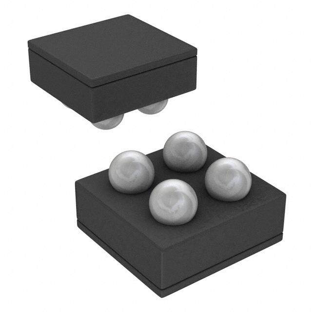
ICGOO电子元器件商城为您提供TMP100NA/250由Texas Instruments设计生产,在icgoo商城现货销售,并且可以通过原厂、代理商等渠道进行代购。 TMP100NA/250价格参考¥6.64-¥14.95。Texas InstrumentsTMP100NA/250封装/规格:温度传感器 - 模拟和数字输出, Temperature Sensor Digital, Local -55°C ~ 125°C 11 b SOT-23-6。您可以下载TMP100NA/250参考资料、Datasheet数据手册功能说明书,资料中有TMP100NA/250 详细功能的应用电路图电压和使用方法及教程。
TMP100NA/250是Texas Instruments(德州仪器)生产的一款高精度数字温度传感器,属于温度传感器中的模拟与数字输出类别。该器件通过I²C/SMBus接口输出数字温度数据,具有典型精度±1°C(在+30°C至+70°C范围内),分辨率可达0.0625°C,无需外部元件即可实现高可靠性测温。

TMP100NA/250广泛应用于对空间和功耗敏感的电子设备中,常见使用场景包括:便携式设备(如智能手机、平板电脑和可穿戴设备),用于监测电池或主控芯片温度,防止过热;计算机与服务器系统中的主板或内存模块温度监控;工业控制设备中的环境温度检测;消费类电子产品如打印机、电源适配器和家电控制器等;此外,也适用于医疗设备中对体温或环境温度进行精确采集的场合。

该传感器采用小型SOT-23-6封装,占用PCB面积小,适合高密度布局设计。其低工作电流(典型值约50μA)和关断模式(功耗仅0.1μA)显著延长了电池供电设备的续航时间。同时,支持多达8个地址的I²C总线配置,便于多点温度监测系统的搭建。

综上所述,TMP100NA/250凭借高精度、小尺寸、低功耗和易集成等优势,成为各类电子系统中实现可靠温度监控的理想选择。
| 参数 | 数值 |
| 产品目录 | 集成电路 (IC)热管理产品 |
| 描述 | IC TEMP SENSOR DIGITAL SOT-23-6板上安装温度传感器 Digital Temp Sensor w/I2C Ser Interface |
| 产品分类 | |
| 品牌 | Texas Instruments |
| 产品手册 | |
| 产品图片 |
|
| rohs | 符合RoHS无铅 / 符合限制有害物质指令(RoHS)规范要求 |
| 产品系列 | 板上安装温度传感器,Texas Instruments TMP100NA/250- |
| 数据手册 | |
| 产品型号 | TMP100NA/250 |
| PCN其它 | |
| 产品目录页面 | |
| 产品种类 | 板上安装温度传感器 |
| 传感器类型 | 内部 |
| 供应商器件封装 | SOT-23-6 |
| 关闭 | Shutdown |
| 其它名称 | 296-12749-1 |
| 准确性 | +/- 3 C |
| 功能 | 温度监控系统(传感器) |
| 包装 | 剪切带 (CT) |
| 商标 | Texas Instruments |
| 安装类型 | 表面贴装 |
| 安装风格 | SMD/SMT |
| 封装 | Reel |
| 封装/外壳 | SOT-23-6 |
| 封装/箱体 | SOT-23-6 |
| 工作温度 | -55°C ~ 125°C |
| 工厂包装数量 | 250 |
| 感应温度 | -55°C ~ 125°C |
| 拓扑 | ADC,寄存器库 |
| 数字输出-位数 | 9 bit to 12 bit |
| 数字输出-总线接口 | 2-Wire, I2C, SMBus |
| 最大工作温度 | + 125 C |
| 最小工作温度 | - 55 C |
| 标准包装 | 1 |
| 温度阈值 | Programmable |
| 电压-电源 | 2.7 V ~ 5.5 V |
| 电源电压-最大 | 5.5 V |
| 电源电压-最小 | 2.7 V |
| 电源电流 | 75 uA |
| 精度 | ±3°C(最大) |
| 系列 | TMP100 |
| 设备功能 | Sensor |
| 输出报警 | 是 |
| 输出电流 | 4 mA |
| 输出类型 | I²C/SMBus |
| 输出风扇 | 无 |
| 配用 | /product-detail/zh/TMP100EVM/296-21135-ND/1216741 |
| 配置 | Local |


- 商务部:美国ITC正式对集成电路等产品启动337调查
- 曝三星4nm工艺存在良率问题 高通将骁龙8 Gen1或转产台积电
- 太阳诱电将投资9.5亿元在常州建新厂生产MLCC 预计2023年完工
- 英特尔发布欧洲新工厂建设计划 深化IDM 2.0 战略
- 台积电先进制程称霸业界 有大客户加持明年业绩稳了
- 达到5530亿美元!SIA预计今年全球半导体销售额将创下新高
- 英特尔拟将自动驾驶子公司Mobileye上市 估值或超500亿美元
- 三星加码芯片和SET,合并消费电子和移动部门,撤换高东真等 CEO
- 三星电子宣布重大人事变动 还合并消费电子和移动部门
- 海关总署:前11个月进口集成电路产品价值2.52万亿元 增长14.8%


PDF Datasheet 数据手册内容提取
Product Sample & Technical Tools & Support & Folder Buy Documents Software Community TMP100,TMP101 SBOS231I–JANUARY2002–REVISEDNOVEMBER2015 2 TMP10x Temperature Sensor With I C and SMBus Interface with Alert Function in SOT-23 Package 1 Features 3 Description • DigitalOutput:SMBus™,Two-Wire,andI2C The TMP100 and TMP101 devices are digital 1 temperature sensors ideal for negative temperature InterfaceCompatibility coefficient (NTC) and positive temperature coefficient • Resolution:9to12Bits,User-Selectable (PTC) thermistor replacement. The devices offer a • Accuracy: typical accuracy of ±1°C without requiring calibration – ±1°C(Typical)from–55°Cto125°C or external component signal conditioning. Device temperature sensors are highly linear and do not – ±2°C(Maximum)from–55°Cto125°C require complex calculations or look-up tables to • LowQuiescentCurrent:45-μA,0.1-μAStandby derive the temperature. The on-chip, 12-bit ADC • WideSupplyRange:2.7Vto5.5V offers resolutions down to 0.0625°C. The devices are availablein6-PinSOT-23packages. • TMP100FeaturesTwoAddressPins • TMP101FeaturesOneAddressPinandan The TMP100 and TMP101 devices feature SMBus, Two-Wire, and I2C interface compatibility. The ALERTPin TMP100 device allows up to eight devices on one • 6-PinSOT-23Package bus. The TMP101 device offers an SMBus Alert functionwithuptothreedevicesperbus. 2 Applications The TMP100 and TMP101 devices are ideal for • Power-SupplyTemperatureMonitoring extended temperature measurement in a variety of • ComputerPeripheralThermalProtection communication, computer, consumer, environmental, • NotebookComputers industrial,andinstrumentationapplications. • CellPhones The TMP100 and TMP101 devices are specified for operation over a temperature range of −55°C to • BatteryManagement 125°C. • OfficeMachines • ThermostatControls DeviceInformation(1) • EnvironmentalMonitoringandHVAC PARTNUMBER PACKAGE BODYSIZE(NOM) • ElectromechanicalDeviceTemperature TMP100 SOT-23(6) 2.90mm×1.60mm TMP101 SOT-23(6) 2.90mm×1.60mm (1) For all available packages, see the orderable addendum at theendofthedatasheet. SimplifiedSchematics Temperature Temperature Diode Diode 1 Control 6 1 Control 6 SCL Temp. SDA SCL Temp. SDA Logic Logic Sensor Sensor ∆Σ ∆Σ 2 Serial 5 2 Serial 5 GND ADC ADD0 GND ADC ADD0 Interface Interface Converter Converter Config Config 3 4 3 4 ADD1 OSC andTemp V+ ALERT OSC andTemp V+ Register Register TMP100 TMP101 1 An IMPORTANT NOTICE at the end of this data sheet addresses availability, warranty, changes, use in safety-critical applications, intellectualpropertymattersandotherimportantdisclaimers.PRODUCTIONDATA.
TMP100,TMP101 SBOS231I–JANUARY2002–REVISEDNOVEMBER2015 www.ti.com Table of Contents 1 Features.................................................................. 1 7.3 FeatureDescription...................................................9 2 Applications........................................................... 1 7.4 DeviceFunctionalModes........................................14 3 Description............................................................. 1 7.5 Programming...........................................................15 4 RevisionHistory..................................................... 2 8 ApplicationandImplementation........................ 19 8.1 ApplicationInformation............................................19 5 PinConfigurationandFunctions......................... 3 8.2 TypicalApplication..................................................19 6 Specifications......................................................... 4 9 PowerSupplyRecommendations...................... 21 6.1 AbsoluteMaximumRatings......................................4 10 Layout................................................................... 21 6.2 ESDRatings ............................................................4 6.3 RecommendedOperatingConditions.......................4 10.1 LayoutGuidelines.................................................21 6.4 ThermalInformation .................................................4 10.2 LayoutExamples...................................................21 6.5 ElectricalCharacteristics...........................................5 11 DeviceandDocumentationSupport................. 23 6.6 TimingRequirements................................................6 11.1 RelatedLinks........................................................23 6.7 TypicalCharacteristics..............................................7 11.2 Trademarks...........................................................23 7 DetailedDescription.............................................. 8 11.3 ElectrostaticDischargeCaution............................23 7.1 Overview...................................................................8 11.4 Glossary................................................................23 7.2 FunctionalBlockDiagram.........................................8 12 Mechanical,Packaging,andOrderable Information........................................................... 23 4 Revision History ChangesfromRevisionH(March2015)toRevisionI Page • ChangedbodysizevaluesinDeviceInformationtable ........................................................................................................ 1 ChangesfromRevisionG(November2007)toRevisionH Page • AddedESDRatingstable,FeatureDescriptionsection,DeviceFunctionalModes,ApplicationandImplementation section,PowerSupplyRecommendationssection,Layoutsection,DeviceandDocumentationSupportsection,and Mechanical,Packaging,andOrderableInformationsection. ................................................................................................ 1 • ChangedspecificationvaluesinTimingRequirementstable ................................................................................................ 6 2 SubmitDocumentationFeedback Copyright©2002–2015,TexasInstrumentsIncorporated ProductFolderLinks:TMP100 TMP101
TMP100,TMP101 www.ti.com SBOS231I–JANUARY2002–REVISEDNOVEMBER2015 5 Pin Configuration and Functions DBVPackage 6-PinSOT-23 TopView T SCL 1 6 SDA 1 GND 2 5 ADD0 0 ADD1 3 0 4 V+ TMP100 DBVPackage 6-PinSOT-23 TopView T SCL 1 6 SDA 1 GND 2 5 ADD0 0 ALERT 3 4 V+ 1 TMP101 PinFunctions PIN NO. I/O DESCRIPTION NAME TMP100 TMP101 ADD0 5 5 I Addressselect.ConnecttoGND,V+,orleavefloating. ADD1 3 — I Addressselect.ConnecttoGND,V+,orleavefloating. ALERT — 3 O Overtemperaturealert.Open-drainoutput;requiresapullupresistor. GND 2 2 — Ground SCL 1 1 I Serialclock.Open-drainoutput;requiresapullupresistor. SDA 6 6 I/O Serialdata.Open-drainoutput;requiresapullupresistor. V+ 4 4 I Supplyvoltage,2.7Vto5.5V Copyright©2002–2015,TexasInstrumentsIncorporated SubmitDocumentationFeedback 3 ProductFolderLinks:TMP100 TMP101
TMP100,TMP101 SBOS231I–JANUARY2002–REVISEDNOVEMBER2015 www.ti.com 6 Specifications 6.1 Absolute Maximum Ratings overoperatingfree-airtemperaturerange(unlessotherwisenoted)(1) MIN MAX UNIT Powersupply,V+ 7.5 V Inputvoltage(2) –0.5 7.5 V Operatingtemperature –55 125 °C Junctiontemperature,T 150 °C J Storagetemperature,T –60 150 °C stg (1) StressesbeyondthoselistedunderAbsoluteMaximumRatingsmaycausepermanentdamagetothedevice.Thesearestressratings only,whichdonotimplyfunctionaloperationofthedeviceattheseoranyotherconditionsbeyondthoseindicatedunderRecommended OperatingConditions.Exposuretoabsolute-maximum-ratedconditionsforextendedperiodsmayaffectdevicereliability. (2) InputvoltageratingappliestoallTMP100andTMP101inputvoltages. 6.2 ESD Ratings VALUE UNIT Humanbodymodel(HBM),perANSI/ESDA/JEDECJS-001(1) ±2000 V Electrostaticdischarge V (ESD) Chargeddevicemodel(CDM),perJEDECspecificationJESD22-C101(2) ±200 (1) JEDECdocumentJEP155statesthat500-VHBMallowssafemanufacturingwithastandardESDcontrolprocess. (2) JEDECdocumentJEP157statesthat250-VCDMallowssafemanufacturingwithastandardESDcontrolprocess. 6.3 Recommended Operating Conditions overoperatingfree-airtemperaturerange(unlessotherwisenoted) MIN NOM MAX UNIT Supplyvoltage 2.7 5.5 V Operatingfree-airtemperature,T –55 125 °C A 6.4 Thermal Information TMP100,TMP101 THERMALMETRIC(1) DBV(SOT-23) UNIT 6PINS R Junction-to-ambientthermalresistance 182.9 °C/W θJA R Junction-to-case(top)thermalresistance 115 °C/W θJC(top) R Junction-to-boardthermalresistance 30.2 °C/W θJB ψ Junction-to-topcharacterizationparameter 17.1 °C/W JT ψ Junction-to-boardcharacterizationparameter 29.7 °C/W JB (1) Formoreinformationabouttraditionalandnewthermalmetrics,seetheICPackageThermalMetricsapplicationreport,SPRA953. 4 SubmitDocumentationFeedback Copyright©2002–2015,TexasInstrumentsIncorporated ProductFolderLinks:TMP100 TMP101
TMP100,TMP101 www.ti.com SBOS231I–JANUARY2002–REVISEDNOVEMBER2015 6.5 Electrical Characteristics AtT =−55°Cto125°CandV+=2.7Vto5.5V,unlessotherwisenoted. A PARAMETER TESTCONDITIONS MIN TYP MAX UNIT TEMPERATUREINPUT Range –55 125 °C −25°Cto85°C ±0.5 ±2 Accuracy(temperatureerror) °C −55°Cto125°C ±1 ±2 Accuracy(temperatureerror)vssupply 0.2 ±0.5 °C/V Resolution Selectable 0.0625 °C DIGITALINPUT/OUTPUT Inputcapacitance 3 pF VIH High-levelinputlogic 0.7(V+) 6 V VIL Low-levelinputlogic −0.5 0.3(V+) V IIN Inputcurrent 0V≤VIN≤6V 1 µA VOL Low-leveloutputlogicSDA IOL=3mA 0 0.15 0.4 V VOL Low-leveloutputlogicALERT IOL=4mA 0 0.15 0.4 V Resolution Selectable 9 12 Bits 9bits 40 75 10bits 80 150 Conversiontime ms 11bits 160 300 12bits 320 600 9bits 25 10bits 12 Conversionrate s/s 11bits 6 12bits 3 POWERSUPPLY Operatingrange 2.7 5.5 V Serialbusinactive 45 75 IQ Quiescentcurrent Serialbusactive,SCLfrequency=400kHz 70 µA Serialbusactive,SCLfrequency=3.4MHz 150 Serialbusinactive 0.1 13 ISD Shutdowncurrent Serialbusactive,SCLfrequency=400kHz 20 µA Serialbusactive,SCLfrequency=3.4MHz 100 TEMPERATURERANGE Specifiedrange –55 125 °C Storagerange –60 150 °C Copyright©2002–2015,TexasInstrumentsIncorporated SubmitDocumentationFeedback 5 ProductFolderLinks:TMP100 TMP101
TMP100,TMP101 SBOS231I–JANUARY2002–REVISEDNOVEMBER2015 www.ti.com 6.6 Timing Requirements FASTMODE HIGH-SPEEDMODE PARAMETER UNIT MIN MAX MIN MAX f SCLoperatingfrequency 0.4 2 MHz (SCL) t BusfreetimebetweenSTOPandSTARTcondition 1300 160 ns (BUF) HoldtimeafterrepeatedSTARTcondition. t 600 160 ns (HDSTA) Afterthisperiod,thefirstclockisgenerated. t RepeatedSTARTconditionsetuptime 600 160 ns (SUSTA) t STOPconditionsetuptime 600 160 ns (SUSTO) t Dataholdtime 20 900 20 170 ns (HDDAT) t Datasetuptime 100 20 ns (SUDAT) t SCLclockLOWperiod 1300 360 ns (LOW) t SCLclockHIGHperiod 600 60 ns (HIGH) t ,t Clockriseandfalltime 300 40 ns RC FC t ,t Datariseandfalltime 300 170 ns RD FD 6 SubmitDocumentationFeedback Copyright©2002–2015,TexasInstrumentsIncorporated ProductFolderLinks:TMP100 TMP101
TMP100,TMP101 www.ti.com SBOS231I–JANUARY2002–REVISEDNOVEMBER2015 6.7 Typical Characteristics AtT =25°CandV+=5V,unlessotherwisenoted. A 70 1 0.9 0.8 60 0.7 V+=5V 0.6 A) A) 0.5 µI(Q 50 µI(SD 00..43 V+= 27 V 0.2 40 0.1 0 SerialBusInactive 30 −0.1 −60 −40 −20 0 20 40 60 80 100 120 140 −60 −40 −20 0 20 40 60 80 100 120 140 Temperature(°C) Temperature (°C) Figure1.QuiescentCurrentvsTemperature Figure2.ShutdownCurrentvsTemperature 400 2.0 1.5 s) C) 1.0 sionTime(m 350 V+=5V °atureError( 00..50 er er −0.5 v 300 p Con V+=2.7V Tem −1.0 −1.5 NOTE:12−bitresolution. 3TypicalUnits NOTE:12−bitresolution. 250 −2.0 −60 −40 −20 0 20 40 60 80 100 120 140 −60 −40 −20 0 20 40 60 80 100 120 140 Temperature(°C) Temperature(°C) Figure3.ConversionTimevsTemperature Figure4.TemperatureAccuracyvsTemperature 180 160 125°C 140 25°C 120 A) 100 µ 125°C ( Q 80 I 25°C −55°C 60 40 −55°C 20 FASTMODE HsMODE 0 10k 100k 1M 10M SCLFrequency(Hz) Figure5.QuiescentCurrentWithBusActivityvsTemperature Copyright©2002–2015,TexasInstrumentsIncorporated SubmitDocumentationFeedback 7 ProductFolderLinks:TMP100 TMP101
TMP100,TMP101 SBOS231I–JANUARY2002–REVISEDNOVEMBER2015 www.ti.com 7 Detailed Description 7.1 Overview The TMP100 and TMP101 devices are digital temperature sensors optimal for thermal management and thermal protection applications. The TMP100 and TMP101 devices are Two-Wire, SMBus, and I2C interface-compatible. These devices are specified over a operating temperature range of −55°C to 125°C. The Functional Block DiagramsectionshowstheinternalblockdiagramsoftheTMP100andTMP101devices. The temperature sensor in the TMP100 and TMP101 devices is the chip itself. Thermal paths run through the package leads as well as the plastic package. The package leads provide the primary thermal path because of the lower thermal resistance of the metal. The GND pin of the TMP100 or TMP101 is directly connected to the metalleadframe,andisthebestchoiceforthermalinput. 7.2 Functional Block Diagram Temperature Temperature Diode Diode 1 Control 6 1 Control 6 SCL Temp. SDA SCL Temp. SDA Logic Logic Sensor Sensor ∆Σ ∆Σ 2 Serial 5 2 Serial 5 GND ADC ADD0 GND ADC ADD0 Interface Interface Converter Converter Config Config 3 4 3 4 ADD1 OSC andTemp V+ ALERT OSC andTemp V+ Register Register TMP100 TMP101 8 SubmitDocumentationFeedback Copyright©2002–2015,TexasInstrumentsIncorporated ProductFolderLinks:TMP100 TMP101
TMP100,TMP101 www.ti.com SBOS231I–JANUARY2002–REVISEDNOVEMBER2015 7.3 Feature Description 7.3.1 DigitalTemperatureOutput The digital output from each temperature measurement conversion is stored in the read-only Temperature Register. The Temperature Register of the TMP100 or TMP101 device is a 12-bit, read-only register that stores the output of the most recent conversion. Two bytes must be read to obtain data and are listed in Table 6 and Table 7. The first 12 bits are used to indicate temperature with all the remaining bits equal to zero. The data format for temperature is listed in Table 1. Negative numbers are represented in binary twos complement format. Followingpower-uporreset,thetemperatureregisterreads0°Cuntilthefirstconversioniscomplete. The user can obtain 9, 10, 11, or 12 bits of resolution by addressing the Configuration Register and setting the resolution bits accordingly. For 9-, 10-, or 11-bit resolution, the most significant bits (MSBs) in the Temperature Registerareusedwiththeunusedleastsignificantbits(LSBs)settozero. Table1.TemperatureDataFormat TEMPERATURE DIGITALOUTPUT (°C) BINARY HEX 128 011111111111 7FF 127.9375 011111111111 7FF 100 011001000000 640 80 010100000000 500 75 010010110000 4B0 50 001100100000 320 25 000110010000 190 0.25 000000000100 004 0 000000000000 000 –0.25 111111111100 FFC –25 111001110000 E70 –55 110010010000 C90 –128 100000000000 800 7.3.2 SerialInterface The TMP100 and TMP101 devices operate only as slave devices on the SMBus, Two-Wire, and I2C interface- compatible bus. Connections to the bus are made through the open-drain I/O lines SDA and SCL. The TMP100 and TMP101 devices support the transmission protocol for fast (up to 400 kHz) and high-speed (up to 2 MHz) modes.AlldatabytesaretransmittedMSBfirst. 7.3.2.1 BusOverview The device that initiates the transfer is called a master, and the devices controlled by the master are slaves. The bus must be controlled by a master device that generates the serial clock (SCL), controls the bus access, and generatestheSTARTandSTOPconditions. Toaddressaspecificdevice,aSTARTconditionisinitiated,indicatedbypullingthedataline(SDA)fromaHIGH to LOW logic level while SCL is HIGH. All slaves on the bus shift in the slave address byte, with the last bit indicating whether a read or write operation is intended. During the ninth clock pulse, the slave being addressed respondstothemasterbygeneratinganAcknowledgeandpullingSDALOW. Data transfer is then initiated and sent over eight clock pulses followed by an Acknowledge Bit. During data transfer, SDA must remain stable while SCL is HIGH because any change in SDA while SCL is HIGH is interpretedasacontrolsignal. When all data are transferred, the master generates a STOP condition indicated by pulling SDA from LOW to HIGH,whileSCLisHIGH. Copyright©2002–2015,TexasInstrumentsIncorporated SubmitDocumentationFeedback 9 ProductFolderLinks:TMP100 TMP101
TMP100,TMP101 SBOS231I–JANUARY2002–REVISEDNOVEMBER2015 www.ti.com 7.3.2.2 SerialBusAddress To program the TMP100 and TMP101 devices, the master must first address slave devices through a slave address byte. The slave address byte consists of seven address bits and a direction bit indicating the intent of executingareadorwriteoperation. The TMP100 device features two address pins to allow up to eight devices to be addressed on a single I2C interface. Table 2 describes the pin logic levels used to properly connect up to eight devices. Float indicates the pin is left unconnected. The state of pins ADD0 and ADD1 is sampled on the first I2C bus communication and mustbesetbeforeanyactivityontheinterface. Table2.AddressPinsandSlaveAddressesfortheTMP100 ADD1 ADD0 SLAVEADDRESS 0 0 1001000 0 Float 1001001 0 1 1001010 1 0 1001100 1 Float 1001101 1 1 1001110 Float 0 1001011 Float 1 1001111 The TMP101 device features one address pin and an ALERT pin, allowing up to three devices to be connected per bus. Pin logic levels are described in Table 3. The address pins of the TMP100 and TMP101 devices are read after reset or in response to an I2C address acquire request. Following reading, the state of the address pinsislatchedtominimizepowerdissipationassociatedwithdetection. Table3.AddressPinsandSlaveAddressesfortheTMP101 ADD0 SLAVEADDRESS 0 1001000 Float 1001001 1 1001010 7.3.2.3 WritingandReadingtotheTMP100andTMP101 Accessing a particular register on the TMP100 and TMP101 devices is accomplished by writing the appropriate value to the Pointer Register. The value for the Pointer Register is the first byte transferred after the I2C slave address byte with the R/W bit LOW. Every write operation to the TMP100 and TMP101 devices requires a value forthePointerRegister(seeFigure7). When reading from the TMP100 and TMP101 devices, the last value stored in the Pointer Register by a write operation is used to determine which register is read by a read operation. To change the register pointer for a read operation, a new value must be written to the Pointer Register. This action is accomplished by issuing an I2C slave address byte with the R/W bit LOW, followed by the Pointer Register Byte. No additional data are required.ThemastercanthengenerateaSTARTconditionandsendtheI2CslaveaddressbytewiththeR/Wbit HIGH to initiate the read command; see Figure 8 for details of this sequence. If repeated reads from the same register are desired, the Pointer Register bytes do not have to be continually sent because the TMP100 and TMP101devicesrememberthePointerRegistervalueuntilthatvalueischangedbythenextwriteoperation. 10 SubmitDocumentationFeedback Copyright©2002–2015,TexasInstrumentsIncorporated ProductFolderLinks:TMP100 TMP101
TMP100,TMP101 www.ti.com SBOS231I–JANUARY2002–REVISEDNOVEMBER2015 7.3.2.4 SlaveModeOperations TheTMP100andTMP101devicescanoperateasaslavereceiverorslavetransmitter. 7.3.2.4.1 SlaveReceiverMode The first byte transmitted by the master is the slave address, with the R/W bit LOW. The TMP100 or TMP101 devices then acknowledges reception of a valid address. The next byte transmitted by the master is the Pointer Register. The TMP100 or TMP101 devices then acknowledges reception of the Pointer Register byte. The next byte or bytes are written to the register addressed by the Pointer Register. The TMP100 and TMP101 devices acknowledge reception of each data byte. The master can terminate data transfer by generating a START or STOPcondition. 7.3.2.4.2 SlaveTransmitterMode The first byte is transmitted by the master and is the slave address, with the R/W bit HIGH. The slave acknowledges reception of a valid slave address. The next byte is transmitted by the slave and is the most significant byte of the register indicated by the Pointer Register. The master acknowledges reception of the data byte. The next byte transmitted by the slave is the least significant byte. The master acknowledges reception of thedatabyte.ThemastercanterminatedatatransferbygeneratingaNot-Acknowledgeonreceptionofanydata byte,orgeneratingaSTARTorSTOPcondition. 7.3.2.5 SMBusAlertFunction The TMP101 device supports the SMBus Alert function. When the TMP101 device is operating in Interrupt Mode (TM = 1), the ALERT pin of the TMP101 device can be connected as an SMBus Alert signal. When a master senses that an ALERT condition is present on the ALERT line, the master sends an SMBus Alert command (00011001) on the bus. If the ALERT pin of the TMP101 device is active, the TMP101 device acknowledges the SMBus Alert command and responds by returning its slave address on the SDA line. The eighth bit (LSB) of the slave address byte indicates if the temperature exceeding T or falling below T caused the ALERT HIGH LOW condition. For POL = 0, this bit is LOW if the temperature is greater than or equal to THIGH. This bit is HIGH if the temperature is less than TLOW. The polarity of this bit is inverted if POL = 1; see Figure 9 for details of this sequence. If multiple devices on the bus respond to the SMBus Alert command, arbitration during the slave address portion of the SMBus alert command determine which device clears its ALERT status. If the TMP101 device wins the arbitration, its ALERT pin becomes inactive at the completion of the SMBus Alert command. If the TMP101 loses thearbitration,itsALERTpinremainsactive. The TMP100 device also responds to the SMBus ALERT command if its TM bit is set to 1. Because the device does not have an ALERT pin, the device must periodically poll the device by issuing an SMBus Alert command. If the TMP100 device generates an ALERT, the device acknowledges the SMBus Alert command and returns its slaveaddressinthenextbyte. 7.3.2.6 GeneralCall The TMP100 and TMP101 devices respond to the I2C General Call address (0000000) if the eighth bit is 0. The device acknowledges the General Call address and responds to commands in the second byte. If the second byteis00000100,theTMP100andTMP101deviceslatchthestatusoftheiraddresspins,butdonotreset.Ifthe second byte is 00000110, the TMP100 and TMP101 devices latch the status of their address pins and reset their internalregisters. 7.3.2.7 High-SpeedMode In order for the I2C bus to operate at frequencies above 400 kHz, the master device must issue an Hs-mode master code (00001XXX) as the first byte after a START condition to switch the bus to high-speed operation. The TMP100 and TMP101 devices do not acknowledge this byte as required by the I2C specification, but do switch their input filters on SDA and SCL and their output filters on SDA to operate in Hs-mode, allowing transfers at up to 2 MHz. After the Hs-mode master code is issued, the master transmits an I2C slave address to initiate a data transfer operation. The bus continues to operate in Hs-mode until a STOP condition occurs on the bus. Upon receiving the STOP condition, the TMP100 and TMP101 devices switch the input and output filter backtofast-modeoperation. Copyright©2002–2015,TexasInstrumentsIncorporated SubmitDocumentationFeedback 11 ProductFolderLinks:TMP100 TMP101
TMP100,TMP101 SBOS231I–JANUARY2002–REVISEDNOVEMBER2015 www.ti.com 7.3.2.8 POR(Power-OnReset) The TMP100 and TMP101 devices both have on-chip, power-on reset circuits that reset the device to default settings when the device is powered on. This circuit activates when the power supply is less than 0.3 V for more than 100 ms. If the TMP100 and TMP101 devices are powered down by removing supply voltage from the device, but the supply voltage is not assured to be less than 0.3 V, TI recommends issuing a General Call reset commandontheI2CinterfacebustoensurethattheTMP100andTMP101devicesarecompletelyreset. 7.3.3 TimingDiagrams The TMP100 and TMP101 devices are Two-Wire, SMBUs, and I2C interface-compatible. Figure 6 to Figure 9 describe the various operations on the TMP100 and TMP101. The following list provides bus definitions. ParametersforFigure6aredefinedintheTimingRequirementssection. BusIdle:BothSDAandSCLlinesremainHIGH. Start Data Transfer: A change in the state of the SDA line, from HIGH to LOW, while the SCL line is HIGH, definesaSTARTcondition.EachdatatransferisinitiatedwithaSTARTcondition. Stop Data Transfer: A change in the state of the SDA line from LOW to HIGH while the SCL line is HIGH definesaSTOPcondition.EachdatatransferisterminatedwitharepeatedSTARTorSTOPcondition. DataTransfer: ThenumberofdatabytestransferredbetweenaSTARTandaSTOPconditionisnotlimitedand isdeterminedbythemasterdevice.Thereceiveracknowledgesthetransferofdata. Acknowledge: Each receiving device, when addressed, is obliged to generate an Acknowledge bit. A device that acknowledges must pull down the SDA line during the Acknowledge clock pulse in such a way that the SDA line is stable LOW during the HIGH period of the Acknowledge clock pulse. Setup and hold times must be taken into account. On a master receive, the termination of the data transfer can be signaled by the master generating aNot-Acknowledgeonthelastbytethatistransmittedbytheslave. t (LOW) tFC t(HDSTA) t RC SCL t t t t (HDSTA) (HIGH) (SUSTA) (SUSTO) t t (HDDAT) (SUDAT) SDA t (BUF) t t RD FD P S S P Figure6. I2CTimingDiagram 12 SubmitDocumentationFeedback Copyright©2002–2015,TexasInstrumentsIncorporated ProductFolderLinks:TMP100 TMP101
TMP100,TMP101 www.ti.com SBOS231I–JANUARY2002–REVISEDNOVEMBER2015 1 9 1 9 … SCL … SDA 1 0 0 1 A2 A1 A0 R/W 0 0 0 0 0 0 P1 P0 StartBy ACKBy ACKBy Master TMP100orTMP101 TMP100orTMP101 Frame1I2CSlaveAddressByte Frame2PointerRegisterByte 1 9 1 9 SCL (Continued) SDA D7 D6 D5 D4 D3 D2 D1 D0 D7 D6 D5 D4 D3 D2 D1 D0 (Continued) ACKBy ACKBy StopBy TMP100orTMP101 TMP100orTMP101 Master Frame3DataByte1 Frame4DataByte2 Figure7. I2CTimingDiagramforWriteWordFormat 1 9 1 9 … SCL … SDA 1 0 0 1 A2 A1 A0 R/W 0 0 0 0 0 0 P1 P0 StartBy ACKBy ACKBy Master TMP100orTMP101 TMP100orTMP101 Frame1I2CSlaveAddressByte Frame2PointerRegisterByte 1 9 1 9 SCL … (Continued) SDA … 1 0 0 1 A2 A1 A0 R/W D7 D6 D5 D4 D3 D2 D1 D0 (Continued) StartBy ACKBy From ACKBy Master TMP100orTMP101 TMP100orTMP101 Master Frame3I2CSlaveAddressByte Frame4DataByte1ReadRegister 1 9 SCL (Continued) SDA D7 D6 D5 D4 D3 D2 D1 D0 (Continued) From ACKBy StopBy TMP100orTMP101 Master Master Frame5DataByte2ReadRegister Figure8. I2CTimingDiagramforReadWordFormat Copyright©2002–2015,TexasInstrumentsIncorporated SubmitDocumentationFeedback 13 ProductFolderLinks:TMP100 TMP101
TMP100,TMP101 SBOS231I–JANUARY2002–REVISEDNOVEMBER2015 www.ti.com ALERT 1 9 1 9 SCL SDA 0 0 0 1 1 0 0 R/W 1 0 0 1 A2 A1 A0 Status StartBy ACKBy From NACKBy StopBy Master TMP100orTMP101 TMP100orTMP101 Master Master Frame1SMBusALERTResponseAddressByte Frame2SlaveAddressFromTMP100 Figure9. TimingDiagramforSMBusALERT 7.4 Device Functional Modes 7.4.1 ShutdownMode(SD) The Shutdown Mode of the TMP100 and TMP101 devices lets the user save maximum power by shutting down all device circuitry other than the serial interface, which reduces current consumption to less than 1 µA. For the TMP100 and TMP101 devices, Shutdown Mode is enabled when the SD bit is 1. The device shuts down when thecurrentconversioniscompleted.ForSDequalto0,thedevicemaintainscontinuousconversion. 7.4.2 OS/ALERT(OS) The TMP100 and TMP101 devices feature a One-Shot Temperature Measurement Mode. When the device is in Shutdown Mode, writing 1 to the OS/ALERT bit starts a single temperature conversion. The device returns to the shutdown state at the completion of the single conversion. This feature is useful to reduce power consumption in theTMP100andTMP101deviceswhencontinuousmonitoringoftemperatureisnotrequired. Reading the OS/ALERT bit provides information about the Comparator Mode status. The state of the POL bit inverts the polarity of data returned from the OS/ALERT bit. For POL = 0, the OS/ALERT reads as 1 until the temperature equals or exceeds T for the programmed number of consecutive faults, causing the OS/ALERT HIGH bit to read as 0. The OS/ALERT bit continues to read as 0 until the temperature falls below T for the LOW programmed number of consecutive faults when the OS/ALERT bit again reads as 1. The status of the TM bit doesnotaffectthestatusoftheOS/ALERTbit. 7.4.3 ThermostatMode(TM) The Thermostat Mode bit of the TMP101 device indicates to the device whether to operate in Comparator Mode (TM = 0) or Interrupt Mode (TM = 1). For more information on comparator and interrupt modes, see the High- andLow-LimitRegisterssection. 7.4.3.1 ComparatorMode(TM=0) In Comparator Mode (TM = 0), the ALERT pin is activated when the temperature equals or exceeds the value in the T register and remains active until the temperature falls below the value in the T register. For more HIGH LOW informationontheComparatorMode,seetheHigh-andLow-LimitRegisterssection. 7.4.3.2 InterruptMode(TM=1) In Interrupt Mode (TM = 1), the ALERT pin is activated when the temperature exceeds T or goes below the HIGH T registers. The ALERT pin is cleared when the host controller reads the temperature register. For more LOW informationontheinterruptmode,seetheHigh-andLow-LimitRegisterssection. 14 SubmitDocumentationFeedback Copyright©2002–2015,TexasInstrumentsIncorporated ProductFolderLinks:TMP100 TMP101
TMP100,TMP101 www.ti.com SBOS231I–JANUARY2002–REVISEDNOVEMBER2015 7.5 Programming 7.5.1 PointerRegister Figure10showstheinternalregisterstructureoftheTMP100andTMP101devices.The8-bitPointerRegisterof the TMP100 and TMP101 devices is used to address a given data register. The Pointer Register uses the two LSBs to identify which of the data registers respond to a read or write command. Table 4 identifies the bits of the Pointer Register byte. Table 5 describes the pointer address of the registers available in the TMP100 and TMP101devices.Thepower-upresetvalueofP1andP0is00. Pointer Register Temperature Register SCL Configuration Register I/O Control Interface T LOW Register SDA T HIGH Register Figure10. InternalRegisterStructureoftheTMP100andTMP101 7.5.1.1 PointerRegisterByte(pointer=N/A)[reset=00h] Table4.PointerRegisterByte P7 P6 P5 P4 P3 P2 P1 P0 0 0 0 0 0 0 RegisterBits 7.5.1.2 PointerAddressesoftheTMP100andTMP101Registers Table5.PointerAddressesoftheTMP100andTMP101Registers P1 P0 TYPE REGISTER 0 0 Ronly,default TemperatureRegister 0 1 R/W ConfigurationRegister 1 0 R/W T Register LOW 1 1 R/W T Register HIGH Copyright©2002–2015,TexasInstrumentsIncorporated SubmitDocumentationFeedback 15 ProductFolderLinks:TMP100 TMP101
TMP100,TMP101 SBOS231I–JANUARY2002–REVISEDNOVEMBER2015 www.ti.com 7.5.2 TemperatureRegister The Temperature Register of the TMP100 or TMP101 devices is a 12-bit, read-only register that stores the output of the most recent conversion. Two bytes must be read to obtain data, and are described in Table 6 and Table 7. The first 12 bits are used to indicate temperature, with all remaining bits equal to zero. Data format for temperature is summarized in Table 1. Following power-up or reset, the Temperature Register reads 0°C until thefirstconversioniscomplete. Table6.Byte1oftheTemperatureRegister D7 D6 D5 D4 D3 D2 D1 D0 T11 T10 T9 T8 T7 T6 T5 T4 Table7.Byte2oftheTemperatureRegister D7 D6 D5 D4 D3 D2 D1 D0 T3 T2 T1 T0 0 0 0 0 7.5.3 ConfigurationRegister The Configuration Register is an 8-bit read and write register used to store bits that control the operational modes of the temperature sensor. Read and write operations are performed MSB-first. The format of the ConfigurationRegisterfortheTMP100andTMP101devicesisshowninTable8,followedbyabreakdownofthe register bits. The power-up or reset value of the Configuration Register is all bits equal to 0. The OS/ALERT bit readsas1afterpower-uporresetvalue. Table8.ConfigurationRegisterFormat BYTE D7 D6 D5 D4 D3 D2 D1 D0 1 OS/ALERT R1 R0 F1 F0 POL TM SD 7.5.3.1 ShutdownMode(SD) The Shutdown Mode of the TMP100 and TMP101 devices allows the user to save maximum power by shutting downalldevicecircuitryotherthantheserialinterface,whichreducescurrentconsumptiontolessthan1 µA.For the TMP100 and TMP101 devices, Shutdown Mode is enabled when the SD bit is 1. The device shuts down whenthecurrentconversioniscompleted.ForSDequalto0,thedevicemaintainscontinuousconversion. 7.5.3.2 ThermostatMode(TM) The Thermostat Mode bit of the TMP101 device indicates to the device whether to operate in Comparator Mode (TM = 0) or Interrupt Mode (TM = 1). For more information on comparator and interrupt modes, see High- and Low-LimitRegisters. 7.5.3.3 Polarity(POL) The Polarity bit of the TMP101 device lets the user adjust the polarity of the ALERT pin output. If the POL bit is set to 0 (default), the ALERT pin becomes active low. When the POL bit is set to 1, the ALERT pin becomes active high and the state of the ALERT pin is inverted. The operation of the ALERT pin in various modes is illustratedinFigure11. 16 SubmitDocumentationFeedback Copyright©2002–2015,TexasInstrumentsIncorporated ProductFolderLinks:TMP100 TMP101
TMP100,TMP101 www.ti.com SBOS231I–JANUARY2002–REVISEDNOVEMBER2015 T Measured HIGH Temperature T LOW TMP101ALERTPIN (ComparatorMode) POL=0 TMP101ALERTPIN (InterruptMode) POL=0 TMP101ALERTPIN (ComparatorMode) POL=1 TMP101ALERTPIN (InterruptMode) POL=1 Read Read Read Time Figure11. OutputTransferFunctionDiagrams 7.5.3.4 FaultQueue(F1,F0) A fault condition occurs when the measured temperature exceeds the user-defined limits set in the T and HIGH T Registers. Additionally, the number of fault conditions required to generate an alert can be programmed LOW using the Fault Queue. The Fault Queue is provided to prevent a false alert resulting from environmental noise. TheFaultQueuerequiresconsecutivefaultmeasurementsinordertotriggerthealertfunction.Ifthetemperature falls below T before reaching the number of programmed consecutive faults limit, the count is reset to 0. LOW Table 9 defines the number of measured faults that can be programmed to trigger an alert condition in the device. Table9.FaultSettingsoftheTMP100andTMP101 F1 F0 CONSECUTIVEFAULTS 0 0 1 0 1 2 1 0 4 1 1 6 7.5.3.5 ConverterResolution(R1,R0) The Converter Resolution bits control the resolution of the internal analog-to-digital converter (ADC), thus allowing the user to maximize efficiency by programming for higher resolution or faster conversion time. Table 10 identifiestheResolutionbitsandtherelationshipbetweenresolutionandconversiontime. Table10.ResolutionoftheTMP100andTMP101 CONVERSIONTIME R1 R0 RESOLUTION (Typical) 0 0 9bits(0.5°C) 40ms 0 1 10bits(0.25°C) 80ms 1 0 11bits(0.125°C) 160ms 1 1 12bits(0.0625°C) 320ms Copyright©2002–2015,TexasInstrumentsIncorporated SubmitDocumentationFeedback 17 ProductFolderLinks:TMP100 TMP101
TMP100,TMP101 SBOS231I–JANUARY2002–REVISEDNOVEMBER2015 www.ti.com 7.5.3.6 OS/ALERT(OS) The TMP100 and TMP101 devices feature a One-Shot Temperature Measurement Mode. When the device is in Shutdown Mode, writing 1 to the OS/ALERT bit starts a single temperature conversion. The device returns to the shutdown state at the completion of the single conversion. This feature is useful to reduce power consumption in theTMP100andTMP101whencontinuoustemperaturemonitoringisnotrequired. Reading the OS/ALERT bit provides information about the Comparator Mode status. The state of the POL bit inverts the polarity of data returned from the OS/ALERT bit. For POL = 0, the OS/ALERT reads as 1 until the temperature equals or exceeds T for the programmed number of consecutive faults, causing the OS/ALERT HIGH bit to read as 0. The OS/ALERT bit continues to read as 0 until the temperature falls below T for the LOW programmed number of consecutive faults when the OS/ALERT bit again reads as 1. The status of the TM bit doesnotaffectthestatusoftheOS/ALERTbit. 7.5.4 High-andLow-LimitRegisters In Comparator Mode (TM = 0), the ALERT pin of the TMP101 becomes active when the temperature equals or exceeds the value in T and generates a consecutive number of faults according to fault bits F1 and F0. The HIGH ALERT pin remains active until the temperature falls below the indicated T value for the same number of LOW faults. In Interrupt Mode (TM = 1) the ALERT pin becomes active when the temperature equals or exceeds T for a HIGH consecutive number of fault conditions. The ALERT pin remains active until a read operation of any register occurs or the device successfully responds to the SMBus Alert Response Address. The ALERT pin is also cleared if the device is placed in Shutdown Mode. When the ALERT pin is cleared, it only becomes active again by the temperature falling below TLOW. When the temperature falls below T , the ALERT pin becomes active LOW and remains active until cleared by a read operation of any register or a successful response to the SMBus Alert Response Address. When the ALERT pin is cleared, the above cycle repeats with the ALERT pin becoming active when the temperature equals or exceeds T . The ALERT pin can also be cleared by resetting the HIGH device with the General Call Reset command. This action also clears the state of the internal registers in the device,returningthedevicetoComparatorMode(TM=0). Both operational modes are represented in Figure 11. Table 11, Table 12, Table 13, and Table 14 describe the format for the T and T registers. Power-up reset values for T and T are: T = 80°C and T = HIGH LOW HIGH LOW HIGH LOW 75°C.TheformatofthedataforT andT isthesameasfortheTemperatureRegister. HIGH LOW Table11.Byte1oftheT Register HIGH D7 D6 D5 D4 D3 D2 D1 D0 H11 H10 H9 H8 H7 H6 H5 H4 Table12.Byte2oftheT Register HIGH D7 D6 D5 D4 D3 D2 D1 D0 H3 H2 H1 H0 0 0 0 0 Table13.Byte1oftheT Register LOW D7 D6 D5 D4 D3 D2 D1 D0 L11 L10 L9 L8 L7 L6 L5 L4 Table14.Byte2oftheT Register LOW D7 D6 D5 D4 D3 D2 D1 D0 L3 L2 L1 L0 0 0 0 0 All12bitsfortheTemperature,T ,andT registersareusedinthecomparisonsfortheALERTfunctionfor HIGH LOW all converter resolutions. The three LSBs in T and T can affect the ALERT output even if the converter is HIGH LOW configuredfor9-bitresolution. 18 SubmitDocumentationFeedback Copyright©2002–2015,TexasInstrumentsIncorporated ProductFolderLinks:TMP100 TMP101
TMP100,TMP101 www.ti.com SBOS231I–JANUARY2002–REVISEDNOVEMBER2015 8 Application and Implementation NOTE Information in the following applications sections is not part of the TI component specification, and TI does not warrant its accuracy or completeness. TI’s customers are responsible for determining suitability of components for their purposes. Customers should validateandtesttheirdesignimplementationtoconfirmsystemfunctionality. 8.1 Application Information TheTMP100andTMP101devicesareusedtomeasuretheprintedcircuitboard(PCB)temperatureoftheboard location where the devices are mounted. The TMP100 features two address pins to allow up to eight devices to be addressed on a single I2C interface. The TMP101 device features one address pin and an ALERT pin, allowing up to three devices to be connected per bus. The TMP100 and TMP101 devices require no external components for operation except for pullup resistors on SCL, SDA, and ALERT (TMP101 device), although a 0.1-μFbypasscapacitorisrecommended. The sensing device of the TMP100 and TMP101 devices is the chip itself. Thermal paths run through the package leads as well as the plastic package. The die flag of the lead frame is connected to GND. The lower thermalresistanceofmetalcausestheleadstoprovidetheprimarythermalpath.TheGNDpinoftheTMP100or TMP101deviceisdirectlyconnectedtothemetalleadframe,andisthebestchoiceforthermalinput. 8.2 Typical Application Supply Voltage Supply Voltage 2.7 V to 5.5 V 2.7 V to 5.5 V Supply Bypass Supply Bypass Capacitor Capacitor Pull-Up Resistors 0.01 PF Pull-Up Resistors 0.01 PF 5-k(cid:13)(cid:3) 5-k(cid:13)(cid:3) TMP100 TMP101 HoTstw Coo-Wntirroeller 1 SCL SDA 6 HoTstw Coo-Wntirroeller 1 SCL SDA 6 2 GND ADD0 5 2 GND ADD0 5 3 ADD1 V+ 4 3 ALERT V+ 4 Figure12.TypicalConnectionsoftheTMP100 Figure13.TypicalConnectionsoftheTMP101 8.2.1 DesignRequirements The TMP100 and TMP101 devices require pullup resistors on the SCL, SDA, and ALERT (TMP101 device) pins. The recommended value for the pullup resistor is 5-kΩ. In some applications, the pullup resistor can be lower or higher than 5-kΩ but must not exceed 3 mA of current on the SCL and SDA pins, and must not exceed 4 mA on the ALERT (TMP101) pin. A 0.1-μF bypass capacitor is recommended, as shown in Figure 12 and Figure 13. The SCL, SDA, and ALERT lines can be pulled up to a supply that is equal to or higher than V through the S pullup resistors. For the TMP100, to configure one of eight different addresses on the bus, connect ADD0 and ADD1 to either the GND pin, V+ pin, or float. Float indicates the pin is left unconnected. For the TMP101 device, toconfigureoneofthreedifferentaddressesonthebus,connectADD0toeithertheGNDpin,V+pin,orfloat. 8.2.2 DetailedDesignProcedure Place the TMP100 and TMP101 devices in close proximity to the heat source that must be monitored, with a proper layout for good thermal coupling. This placement ensures that temperature changes are captured within the shortest possible time interval. To maintain accuracy in applications that require air or surface temperature measurement, care must be taken to isolate the package and leads from ambient air temperature. A thermally- conductiveadhesiveishelpfulinachievingaccuratesurfacetemperaturemeasurement. Copyright©2002–2015,TexasInstrumentsIncorporated SubmitDocumentationFeedback 19 ProductFolderLinks:TMP100 TMP101
TMP100,TMP101 SBOS231I–JANUARY2002–REVISEDNOVEMBER2015 www.ti.com Typical Application (continued) 8.2.3 ApplicationCurve Figure 14 shows the step response of the TMP100 and TMP101 devices to a submersion in an oil bath of 100ºC from room temperature (27ºC). The time constant, or the time for the output to reach 63% of the input step, is 0.9 s. The time-constant result depends on the PCB that the TMP100 and TMP101 devices are mounted. For this test, the TMP100 and TMP101 devices are soldered to a two-layer PCB that measures 0.375 inch × 0.437 inch. 100 95 90 85 80 C) 75 qe ( 70 ur 65 erat 60 p 55 m e 50 T 45 40 35 30 25 -1 1 3 5 7 9 11 13 15 17 19 Time (s) Figure14. TemperatureStepResponse 20 SubmitDocumentationFeedback Copyright©2002–2015,TexasInstrumentsIncorporated ProductFolderLinks:TMP100 TMP101
TMP100,TMP101 www.ti.com SBOS231I–JANUARY2002–REVISEDNOVEMBER2015 9 Power Supply Recommendations The TMP100 and TMP101 devices operate with power supply in the range of 2.7 V to 5.5 V. A power-supply bypass capacitor is required for stability; place this capacitor as close as possible to the supply and ground pins of the device. A typical value for this supply bypass capacitor is 0.01 μF. Applications with noisy or high- impedancepowersuppliescanrequireadditionaldecouplingcapacitorstorejectpower-supplynoise. 10 Layout 10.1 Layout Guidelines Place the power-supply bypass capacitor as close as possible to the supply and ground pins. The recommended value of this bypass capacitor is 0.01 μF. Additional decoupling capacitance can be added to compensate for noisy or high-impedance power supplies. Pull up the open-drain output pins SDA , SCL, and ALERT (TMP101) through5-kΩpullupresistors. 10.2 Layout Examples Via to Power or Ground Plane Via to Internal Layer Pull-Up Resistors SCL SDA GND ADD0 Supply Voltage ADD1 V+ Supply Bypass Capacitor Ground Plane for Thermal Coupling to Heat Source Serial Bus Traces Heat Source Figure15. TMP100LayoutExample Copyright©2002–2015,TexasInstrumentsIncorporated SubmitDocumentationFeedback 21 ProductFolderLinks:TMP100 TMP101
TMP100,TMP101 SBOS231I–JANUARY2002–REVISEDNOVEMBER2015 www.ti.com Layout Examples (continued) Via to Power or Ground Plane Via to Internal Layer Pull-Up Resistors SCL SDA GND ADD0 Supply Voltage ALERT V+ Supply Bypass Capacitor Ground Plane for Thermal Coupling to Heat Source Serial Bus Traces Heat Source Figure16. TMP101LayoutExample 22 SubmitDocumentationFeedback Copyright©2002–2015,TexasInstrumentsIncorporated ProductFolderLinks:TMP100 TMP101
TMP100,TMP101 www.ti.com SBOS231I–JANUARY2002–REVISEDNOVEMBER2015 11 Device and Documentation Support 11.1 Related Links The table below lists quick access links. Categories include technical documents, support and community resources,toolsandsoftware,andquickaccesstosampleorbuy. Table15.RelatedLinks TECHNICAL TOOLS& SUPPORT& PARTS PRODUCTFOLDER SAMPLE&BUY DOCUMENTS SOFTWARE COMMUNITY TMP100 Clickhere Clickhere Clickhere Clickhere Clickhere TMP101 Clickhere Clickhere Clickhere Clickhere Clickhere 11.2 Trademarks SMBusisatrademarkofNXPSemiconductors. Allothertrademarksarethepropertyoftheirrespectiveowners. 11.3 Electrostatic Discharge Caution Thesedeviceshavelimitedbuilt-inESDprotection.Theleadsshouldbeshortedtogetherorthedeviceplacedinconductivefoam duringstorageorhandlingtopreventelectrostaticdamagetotheMOSgates. 11.4 Glossary SLYZ022—TIGlossary. Thisglossarylistsandexplainsterms,acronyms,anddefinitions. 12 Mechanical, Packaging, and Orderable Information The following pages include mechanical, packaging, and orderable information. This information is the most current data available for the designated devices. This data is subject to change without notice and revision of thisdocument.Forbrowser-basedversionsofthisdatasheet,refertotheleft-handnavigation. Copyright©2002–2015,TexasInstrumentsIncorporated SubmitDocumentationFeedback 23 ProductFolderLinks:TMP100 TMP101
PACKAGE OPTION ADDENDUM www.ti.com 15-Apr-2017 PACKAGING INFORMATION Orderable Device Status Package Type Package Pins Package Eco Plan Lead/Ball Finish MSL Peak Temp Op Temp (°C) Device Marking Samples (1) Drawing Qty (2) (6) (3) (4/5) SN0312100DBVR ACTIVE SOT-23 DBV 6 3000 Green (RoHS CU NIPDAU Level-2-260C-1 YEAR -55 to 125 T100 & no Sb/Br) TMP100NA/250 ACTIVE SOT-23 DBV 6 250 Green (RoHS CU NIPDAU Level-2-260C-1 YEAR T100 & no Sb/Br) TMP100NA/250G4 ACTIVE SOT-23 DBV 6 250 Green (RoHS CU NIPDAU Level-2-260C-1 YEAR T100 & no Sb/Br) TMP100NA/3K ACTIVE SOT-23 DBV 6 3000 Green (RoHS CU NIPDAU Level-2-260C-1 YEAR -55 to 125 T100 & no Sb/Br) TMP100NA/3KG4 ACTIVE SOT-23 DBV 6 3000 Green (RoHS CU NIPDAU Level-2-260C-1 YEAR -55 to 125 T100 & no Sb/Br) TMP101NA/250 ACTIVE SOT-23 DBV 6 250 Green (RoHS CU NIPDAU Level-2-260C-1 YEAR -55 to 125 T101 & no Sb/Br) TMP101NA/250G4 ACTIVE SOT-23 DBV 6 250 Green (RoHS CU NIPDAU Level-2-260C-1 YEAR -55 to 125 T101 & no Sb/Br) TMP101NA/3K ACTIVE SOT-23 DBV 6 3000 Green (RoHS CU NIPDAU Level-2-260C-1 YEAR -55 to 125 T101 & no Sb/Br) TMP101NA/3KG4 ACTIVE SOT-23 DBV 6 3000 Green (RoHS CU NIPDAU Level-2-260C-1 YEAR -55 to 125 T101 & no Sb/Br) (1) The marketing status values are defined as follows: ACTIVE: Product device recommended for new designs. LIFEBUY: TI has announced that the device will be discontinued, and a lifetime-buy period is in effect. NRND: Not recommended for new designs. Device is in production to support existing customers, but TI does not recommend using this part in a new design. PREVIEW: Device has been announced but is not in production. Samples may or may not be available. OBSOLETE: TI has discontinued the production of the device. (2) Eco Plan - The planned eco-friendly classification: Pb-Free (RoHS), Pb-Free (RoHS Exempt), or Green (RoHS & no Sb/Br) - please check http://www.ti.com/productcontent for the latest availability information and additional product content details. TBD: The Pb-Free/Green conversion plan has not been defined. Pb-Free (RoHS): TI's terms "Lead-Free" or "Pb-Free" mean semiconductor products that are compatible with the current RoHS requirements for all 6 substances, including the requirement that lead not exceed 0.1% by weight in homogeneous materials. Where designed to be soldered at high temperatures, TI Pb-Free products are suitable for use in specified lead-free processes. Pb-Free (RoHS Exempt): This component has a RoHS exemption for either 1) lead-based flip-chip solder bumps used between the die and package, or 2) lead-based die adhesive used between the die and leadframe. The component is otherwise considered Pb-Free (RoHS compatible) as defined above. Green (RoHS & no Sb/Br): TI defines "Green" to mean Pb-Free (RoHS compatible), and free of Bromine (Br) and Antimony (Sb) based flame retardants (Br or Sb do not exceed 0.1% by weight in homogeneous material) Addendum-Page 1
PACKAGE OPTION ADDENDUM www.ti.com 15-Apr-2017 (3) MSL, Peak Temp. - The Moisture Sensitivity Level rating according to the JEDEC industry standard classifications, and peak solder temperature. (4) There may be additional marking, which relates to the logo, the lot trace code information, or the environmental category on the device. (5) Multiple Device Markings will be inside parentheses. Only one Device Marking contained in parentheses and separated by a "~" will appear on a device. If a line is indented then it is a continuation of the previous line and the two combined represent the entire Device Marking for that device. (6) Lead/Ball Finish - Orderable Devices may have multiple material finish options. Finish options are separated by a vertical ruled line. Lead/Ball Finish values may wrap to two lines if the finish value exceeds the maximum column width. Important Information and Disclaimer:The information provided on this page represents TI's knowledge and belief as of the date that it is provided. TI bases its knowledge and belief on information provided by third parties, and makes no representation or warranty as to the accuracy of such information. Efforts are underway to better integrate information from third parties. TI has taken and continues to take reasonable steps to provide representative and accurate information but may not have conducted destructive testing or chemical analysis on incoming materials and chemicals. TI and TI suppliers consider certain information to be proprietary, and thus CAS numbers and other limited information may not be available for release. In no event shall TI's liability arising out of such information exceed the total purchase price of the TI part(s) at issue in this document sold by TI to Customer on an annual basis. OTHER QUALIFIED VERSIONS OF TMP100, TMP101 : •Automotive: TMP101-Q1 •Enhanced Product: TMP100-EP NOTE: Qualified Version Definitions: •Automotive - Q100 devices qualified for high-reliability automotive applications targeting zero defects •Enhanced Product - Supports Defense, Aerospace and Medical Applications Addendum-Page 2
PACKAGE MATERIALS INFORMATION www.ti.com 10-Jul-2018 TAPE AND REEL INFORMATION *Alldimensionsarenominal Device Package Package Pins SPQ Reel Reel A0 B0 K0 P1 W Pin1 Type Drawing Diameter Width (mm) (mm) (mm) (mm) (mm) Quadrant (mm) W1(mm) TMP100NA/250 SOT-23 DBV 6 250 178.0 9.0 3.23 3.17 1.37 4.0 8.0 Q3 TMP100NA/3K SOT-23 DBV 6 3000 178.0 9.0 3.23 3.17 1.37 4.0 8.0 Q3 TMP101NA/250 SOT-23 DBV 6 250 178.0 9.0 3.23 3.17 1.37 4.0 8.0 Q3 TMP101NA/3K SOT-23 DBV 6 3000 178.0 9.0 3.23 3.17 1.37 4.0 8.0 Q3 PackMaterials-Page1
PACKAGE MATERIALS INFORMATION www.ti.com 10-Jul-2018 *Alldimensionsarenominal Device PackageType PackageDrawing Pins SPQ Length(mm) Width(mm) Height(mm) TMP100NA/250 SOT-23 DBV 6 250 180.0 180.0 18.0 TMP100NA/3K SOT-23 DBV 6 3000 180.0 180.0 18.0 TMP101NA/250 SOT-23 DBV 6 250 445.0 220.0 345.0 TMP101NA/3K SOT-23 DBV 6 3000 445.0 220.0 345.0 PackMaterials-Page2
PACKAGE OUTLINE DBV0006A SOT-23 - 1.45 mm max height SCALE 4.000 SMALL OUTLINE TRANSISTOR C 3.0 2.6 0.1 C 1.75 1.45 B A 1.45 MAX PIN 1 INDEX AREA 1 6 2X 0.95 3.05 2.75 1.9 5 2 4 3 0.50 6X 0.25 0.15 0.2 C A B (1.1) TYP 0.00 0.25 GAGE PLANE 0.22 TYP 0.08 8 TYP 0.6 0 0.3 TYP SEATING PLANE 4214840/B 03/2018 NOTES: 1. All linear dimensions are in millimeters. Any dimensions in parenthesis are for reference only. Dimensioning and tolerancing per ASME Y14.5M. 2. This drawing is subject to change without notice. 3. Body dimensions do not include mold flash or protrusion. Mold flash and protrusion shall not exceed 0.15 per side. 4. Leads 1,2,3 may be wider than leads 4,5,6 for package orientation. 5. Refernce JEDEC MO-178. www.ti.com
EXAMPLE BOARD LAYOUT DBV0006A SOT-23 - 1.45 mm max height SMALL OUTLINE TRANSISTOR PKG 6X (1.1) 1 6X (0.6) 6 SYMM 2 5 2X (0.95) 3 4 (R0.05) TYP (2.6) LAND PATTERN EXAMPLE EXPOSED METAL SHOWN SCALE:15X SOLDER MASK SOLDER MASK METAL UNDER METAL OPENING OPENING SOLDER MASK EXPOSED METAL EXPOSED METAL 0.07 MAX 0.07 MIN ARROUND ARROUND NON SOLDER MASK SOLDER MASK DEFINED DEFINED (PREFERRED) SOLDER MASK DETAILS 4214840/B 03/2018 NOTES: (continued) 6. Publication IPC-7351 may have alternate designs. 7. Solder mask tolerances between and around signal pads can vary based on board fabrication site. www.ti.com
EXAMPLE STENCIL DESIGN DBV0006A SOT-23 - 1.45 mm max height SMALL OUTLINE TRANSISTOR PKG 6X (1.1) 1 6X (0.6) 6 SYMM 2 5 2X(0.95) 3 4 (R0.05) TYP (2.6) SOLDER PASTE EXAMPLE BASED ON 0.125 mm THICK STENCIL SCALE:15X 4214840/B 03/2018 NOTES: (continued) 8. Laser cutting apertures with trapezoidal walls and rounded corners may offer better paste release. IPC-7525 may have alternate design recommendations. 9. Board assembly site may have different recommendations for stencil design. www.ti.com
IMPORTANTNOTICEANDDISCLAIMER TIPROVIDESTECHNICALANDRELIABILITYDATA(INCLUDINGDATASHEETS),DESIGNRESOURCES(INCLUDINGREFERENCE DESIGNS),APPLICATIONOROTHERDESIGNADVICE,WEBTOOLS,SAFETYINFORMATION,ANDOTHERRESOURCES“ASIS” ANDWITHALLFAULTS,ANDDISCLAIMSALLWARRANTIES,EXPRESSANDIMPLIED,INCLUDINGWITHOUTLIMITATIONANY IMPLIEDWARRANTIESOFMERCHANTABILITY,FITNESSFORAPARTICULARPURPOSEORNON-INFRINGEMENTOFTHIRD PARTYINTELLECTUALPROPERTYRIGHTS. TheseresourcesareintendedforskilleddevelopersdesigningwithTIproducts.Youaresolelyresponsiblefor(1)selectingtheappropriate TIproductsforyourapplication,(2)designing,validatingandtestingyourapplication,and(3)ensuringyourapplicationmeetsapplicable standards,andanyothersafety,security,orotherrequirements.Theseresourcesaresubjecttochangewithoutnotice.TIgrantsyou permissiontousetheseresourcesonlyfordevelopmentofanapplicationthatusestheTIproductsdescribedintheresource.Other reproductionanddisplayoftheseresourcesisprohibited.NolicenseisgrantedtoanyotherTIintellectualpropertyrightortoanythird partyintellectualpropertyright.TIdisclaimsresponsibilityfor,andyouwillfullyindemnifyTIanditsrepresentativesagainst,anyclaims, damages,costs,losses,andliabilitiesarisingoutofyouruseoftheseresources. TI’sproductsareprovidedsubjecttoTI’sTermsofSale(www.ti.com/legal/termsofsale.html)orotherapplicabletermsavailableeitheron ti.comorprovidedinconjunctionwithsuchTIproducts.TI’sprovisionoftheseresourcesdoesnotexpandorotherwisealterTI’sapplicable warrantiesorwarrantydisclaimersforTIproducts. MailingAddress:TexasInstruments,PostOfficeBox655303,Dallas,Texas75265 Copyright©2019,TexasInstrumentsIncorporated