ICGOO在线商城 > 传感器,变送器 > 温度传感器 - 模拟和数字输出 > SA56004BDP,118
 Datasheet下载
- 型号: SA56004BDP,118
- 制造商: NXP Semiconductors
- 库位|库存: xxxx|xxxx
- 要求:
| 数量阶梯 | 香港交货 | 国内含税 |
| +xxxx | $xxxx | ¥xxxx |
查看当月历史价格
查看今年历史价格
SA56004BDP,118产品简介:
ICGOO电子元器件商城为您提供SA56004BDP,118由NXP Semiconductors设计生产,在icgoo商城现货销售,并且可以通过原厂、代理商等渠道进行代购。 SA56004BDP,118价格参考。NXP SemiconductorsSA56004BDP,118封装/规格:温度传感器 - 模拟和数字输出, 温度传感器 数字,本地/远程 -40°C ~ 125°C 10 b 8-TSSOP。您可以下载SA56004BDP,118参考资料、Datasheet数据手册功能说明书,资料中有SA56004BDP,118 详细功能的应用电路图电压和使用方法及教程。
NXP USA Inc. 的型号 SA56004BDP,118 是一款温度传感器,属于“温度传感器 - 模拟和数字输出”类别。以下是其主要应用场景及特点的详细说明:

 1. 应用场景
   - 消费电子设备:用于智能家电(如冰箱、空调、烤箱等)中监测环境或内部温度,确保设备运行在安全范围内。
   - 工业控制:适用于工业自动化系统中的温度监控,例如电机过热保护、生产线温度调节等。
   - 汽车电子:可用于车内温度监控、发动机冷却系统或电池管理系统(BMS),以优化性能并延长电池寿命。
   - 医疗设备:在体温计、孵化器或其他需要精确温度测量的医疗仪器中提供高精度的温度检测。
   - 通信设备:用于基站、路由器等设备的散热管理,防止因过热导致的故障。

 2. 产品特点
   - 双输出模式:支持模拟和数字输出,灵活性强,可满足不同系统的接口需求。
   - 宽温度范围:通常覆盖从-40°C到+150°C的范围,适应多种极端环境。
   - 高精度:具有较高的温度测量精度,误差小,适合对温度敏感的应用场景。
   - 低功耗:设计注重节能,适合便携式或电池供电的设备。
   - 小型封装:采用紧凑型封装(如SOT-23),便于集成到空间受限的设计中。

 3. 典型应用示例
   - 在智能家居温控系统中,该传感器可以实时监测室内温度,并将数据反馈给控制器以调整加热或制冷设备的工作状态。
   - 在电动汽车电池组中,它能够持续监控每个电池单元的温度,避免过热引发的安全隐患。
   - 在工业烘箱或冷藏柜中,该传感器通过精确的温度反馈实现恒温控制,提高生产效率和产品质量。

总之,SA56004BDP,118 凭借其多功能性和可靠性,广泛应用于需要精确温度监测的各种领域,是现代电子系统中不可或缺的关键组件之一。
| 参数 | 数值 |
| 产品目录 | 集成电路 (IC)热管理产品 |
| 描述 | IC TEMP SENSOR 8-TSSOP板上安装温度传感器 I2C LOC +/- 2OC AND |
| 产品分类 | |
| 品牌 | NXP Semiconductors |
| 产品手册 | |
| 产品图片 |
|
| rohs | 符合RoHS无铅 / 符合限制有害物质指令(RoHS)规范要求 |
| 产品系列 | 板上安装温度传感器,NXP Semiconductors SA56004BDP,118- |
| 数据手册 | |
| 产品型号 | SA56004BDP,118 |
| PCN封装 | |
| 产品目录页面 | |
| 产品种类 | 板上安装温度传感器 |
| 传感器类型 | 内部和外部 |
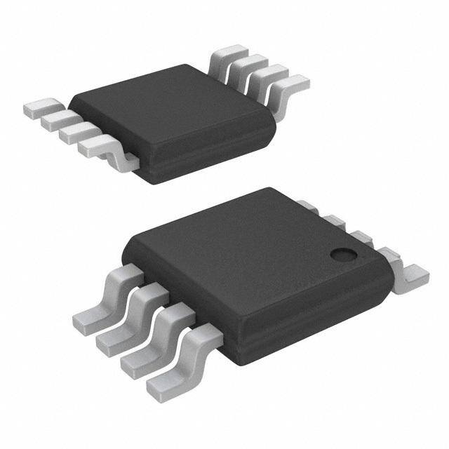
| 供应商器件封装 | 8-TSSOP |
| 关闭 | Shutdown |
| 其它名称 | 568-3332-2 |
| 准确性 | +/- 1 C to +/- 3 C |
| 功能 | 温度监控系统(传感器) |
| 包装 | 带卷 (TR) |
| 商标 | NXP Semiconductors |
| 安装类型 | 表面贴装 |
| 封装 | Reel |
| 封装/外壳 | 8-TSSOP,8-MSOP(0.118",3.00mm 宽) |
| 封装/箱体 | TSSOP-8 |
| 工作温度 | -40°C ~ 125°C |
| 工厂包装数量 | 2500 |
| 感应温度 | -40°C ~ 125°C |
| 拓扑 | ADC(三角积分型),多路复用器,寄存器库 |
| 数字输出-位数 | 11 bit |
| 数字输出-总线接口 | 2-Wire, I2C, SMBus |
| 最大工作温度 | + 125 C |
| 最小工作温度 | - 40 C |
| 标准包装 | 2,500 |
| 温度阈值 | Programmable |
| 特色产品 | http://www.digikey.com/cn/zh/ph/NXP/I2C.html |
| 电压-电源 | 3 V ~ 5.5 V |
| 电源电压-最大 | 5.5 V |
| 电源电压-最小 | 3 V |
| 电源电流 | 500 uA |
| 精度 | ±3°C(最大) |
| 设备功能 | Sensor with Alert |
| 输出报警 | 是 |
| 输出类型 | Digital |
| 输出风扇 | 是 |
| 配用 | /product-detail/zh/OM6275,598/568-3615-ND/1154197 |
| 配置 | Local, Remote |
| 零件号别名 | SA56004BDP-T |


- 商务部:美国ITC正式对集成电路等产品启动337调查
- 曝三星4nm工艺存在良率问题 高通将骁龙8 Gen1或转产台积电
- 太阳诱电将投资9.5亿元在常州建新厂生产MLCC 预计2023年完工
- 英特尔发布欧洲新工厂建设计划 深化IDM 2.0 战略
- 台积电先进制程称霸业界 有大客户加持明年业绩稳了
- 达到5530亿美元!SIA预计今年全球半导体销售额将创下新高
- 英特尔拟将自动驾驶子公司Mobileye上市 估值或超500亿美元
- 三星加码芯片和SET,合并消费电子和移动部门,撤换高东真等 CEO
- 三星电子宣布重大人事变动 还合并消费电子和移动部门
- 海关总署:前11个月进口集成电路产品价值2.52万亿元 增长14.8%


PDF Datasheet 数据手册内容提取
SA56004X SMBus-compatible, 8-pin, remote/local digital temperature sensor with overtemperature alarms Rev. 7 — 25 February 2013 Product data sheet 1. General description The NXP Semiconductors SA56004X is an SMBus compatible, 11-bit remote/local digital temperature sensor with overtemperature alarms. The remote channel of the SA56004X monitors a diode junction, such as a substrate PNP of a microprocessor or a diode connected transistor such as the 2N3904 (NPN) or 2N3906 (PNP). With factory trimming, remote sensor accuracy of 1C is achieved. Undertemperature and overtemperature alert thresholds can be programmed to cause the ALERT output to indicate when the on-chip or remote temperature is out of range. This output may be used as a system interrupt or SMBus alert. The T_CRIT output is activated when the on-chip or remote temperature measurement rises above the programmed T_CRIT threshold register value. This output may be used to activate a cooling fan, send a warning or trigger a system shutdown. To enhance system reliability further, the SA56004X employs an SMBus time-out protocol. The SA56004X has a unique device architecture. The SA56004X is available in the SO8, TSSOP8 and HVSON8 packages. SA56004X has 8factory-programmed device address options. The SA56004X is pin-compatible with the LM86, MAX6657/8, and ADM1032. 2. Features and benefits Accurately senses temperature of remote microprocessor thermal diodes or diode connected transistors within 1C On-chip local temperature sensing within 2C Temperature range of 40C to +125C 11-bit, 0.125C resolution 8 different device addresses are available for server applications. The SA56004ED with marking code 56004E, and SA56004EDP with marking code 6004E are address compatible with the National LM86, the MAX6657/8 and the ADM1032. Offset registers available for adjusting the remote temperature accuracy Programmable under/overtemperature alarms: ALERT and T_CRIT SMBus 2.0 compatible interface, supports TIMEOUT Operating voltage range: 3.0V to 3.6V I2C-bus Standard-mode and Fast-mode compatible SO8, TSSOP8 and HVSON8 packages Programmable conversion rate (0.0625Hz to 26Hz) Undervoltage lockout prevents erroneous temperature readings Latch-up testing is done to JEDEC Standard JESD78 which exceeds 100mA
SA56004X NXP Semiconductors Digital temperature sensor with overtemperature alarms 3. Applications System thermal management in laptops, desktops, servers and workstations Computers and office electronic equipment Electronic test equipment and instrumentation HVAC Industrial controllers and embedded systems 4. Ordering information Table 1. Ordering info rmation Type number[1] Topside Package marking Name Description Version SA56004AD 56004AD SO8 plastic small outline package; 8leads; bodywidth3.9mm SOT96-1 SA56004BD 56004BD SA56004CD 56004CD SA56004DD 56004DD SA56004ED 56004ED SA56004FD 56004FD SA56004GD 56004GD SA56004HD 56004HD SA56004ADP 6004A TSSOP8 plastic thin shrink small outline package; 8leads; bodywidth3mm SOT505-1 SA56004BDP 6004B SA56004CDP 6004C SA56004DDP 6004D SA56004EDP 6004E SA56004FDP 6004F SA56004GDP 6004G SA56004HDP 6004H SA56004ATK 6004A HVSON8 plastic thermal enhanced very thin small outline package; noleads; SOT782-1 8terminals; body330.85mm SA56004ETK 6004E [1] There are 8 device slave address options, as described in Table4. SA56004X All information provided in this document is subject to legal disclaimers. © NXP B.V. 2013. All rights reserved. Product data sheet Rev. 7 — 25 February 2013 2 of 43
SA56004X NXP Semiconductors Digital temperature sensor with overtemperature alarms 4.1 Ordering options Table 2. Ordering opt ions Type number Orderable Package Packing method Minimum Temperature partnumber orderquantity SA56004AD SA56004AD,112 SO8 Tube, bulk pack 2000 T = 40C to +125C amb SA56004AD,118 SO8 Reel pack, SMD, 13-inch 2500 T = 40C to +125C amb SA56004BD SA56004BD,112 SO8 Tube, bulk pack 2000 T = 40C to +125C amb SA56004BD,118 SO8 Reel pack, SMD, 13-inch 2500 T = 40C to +125C amb SA56004CD SA56004CD,112 SO8 Tube, bulk pack 2000 T = 40C to +125C amb SA56004CD,118 SO8 Reel pack, SMD, 13-inch 2500 T = 40C to +125C amb SA56004DD SA56004DD,112 SO8 Tube, bulk pack 2000 T = 40C to +125C amb SA56004DD,118 SO8 Reel pack, SMD, 13-inch 2500 T = 40C to +125C amb SA56004ED SA56004ED,112 SO8 Tube, bulk pack 2000 T = 40C to +125C amb SA56004ED,118 SO8 Reel pack, SMD, 13-inch 2500 T = 40C to +125C amb SA56004FD SA56004FD,112 SO8 Tube, bulk pack 2000 T = 40C to +125C amb SA56004FD,118 SO8 Reel pack, SMD, 13-inch 2500 T = 40C to +125C amb SA56004GD SA56004GD,118 SO8 Reel pack, SMD, 13-inch 2500 T = 40C to +125C amb SA56004HD SA56004HD,112 SO8 Tube, bulk pack 2000 T = 40C to +125C amb SA56004HD,118 SO8 Reel pack, SMD, 13-inch 2500 T = 40C to +125C amb SA56004ADP SA56004ADP,118 TSSOP8 Reel pack, SMD, 13-inch 2500 T = 40C to +125C amb SA56004BDP SA56004BDP,118 TSSOP8 Reel pack, SMD, 13-inch 2500 T = 40C to +125C amb SA56004CDP SA56004CDP,118 TSSOP8 Reel pack, SMD, 13-inch 2500 T = 40C to +125C amb SA56004DDP SA56004DDP,118 TSSOP8 Reel pack, SMD, 13-inch 2500 T = 40C to +125C amb SA56004EDP SA56004EDP,118 TSSOP8 Reel pack, SMD, 13-inch 2500 T = 40C to +125C amb SA56004FDP SA56004FDP,118 TSSOP8 Reel pack, SMD, 13-inch 2500 T = 40C to +125C amb SA56004GDP SA56004GDP,118 TSSOP8 Reel pack, SMD, 13-inch 2500 T = 40C to +125C amb SA56004HDP SA56004HDP,118 TSSOP8 Reel pack, SMD, 13-inch 2500 T = 40C to +125C amb SA56004ATK SA56004ATK,118 HVSON8 Reel pack, SMD, 13-inch 6000 T = 40C to +125C amb SA56004ETK SA56004ETK,118 HVSON8 Reel pack, SMD, 13-inch 6000 T = 40C to +125C amb SA56004X All information provided in this document is subject to legal disclaimers. © NXP B.V. 2013. All rights reserved. Product data sheet Rev. 7 — 25 February 2013 3 of 43
SA56004X NXP Semiconductors Digital temperature sensor with overtemperature alarms 5. Block diagram SA56004X ONE-SHOT VDD REGISTER LOCAL TEMP REMOTE OFFSET CONFIGURATION COMMAND SENSOR CONTROL REGISTER REGISTER REGISTER LOGIC CONVERSION LOCAL HIGH TEMP LOCAL TEMP HIGH REGISTER THRESHOLD LIMIT REGISTER LOCAL TEMP LOCAL LOW TEMP LOCAL TEMP LOW D+ LOCAL 11Σ--BΔIT DATA REGISTER THRESHOLD THRESHOLD REMOTE A-to-D D− MUX REMOTE TEMP REMOTE HIGH REMOTE TEMP CONVERTER DATA REGISTER TEMP THRESHOLD HIGH LIMIT REG. T_CRIT REMOTE LOW REMOTE TEMP HYSTERESIS TEMP THRESHOLD LOW LIMIT REG. ALERT ALERT INTERRUPT STATUS REGISTER GND T_CRIT T_CRIT OTP DEVICE SMBus INTERFACE ADDRESS REGISTER INTERRUPT 002aad202 SDATA SCLK Fig 1. Block diagram SA56004X All information provided in this document is subject to legal disclaimers. © NXP B.V. 2013. All rights reserved. Product data sheet Rev. 7 — 25 February 2013 4 of 43
SA56004X NXP Semiconductors Digital temperature sensor with overtemperature alarms 6. Pinning information 6.1 Pinning VDD 1 8 SCLK VDD 1 8 SCLK D+ 2 7 SDATA D+ 2 7 SDATA SA56004XD SA56004XDP D− 3 6 ALERT D− 3 6 ALERT T_CRIT 4 5 GND T_CRIT 4 5 GND 002aad198 002aad199 Fig 2. Pin configuration for SO8 Fig 3. Pin configuration for TSSOP8 terminal 1 index area VDD 1 8 SCLK D+ 2 7 SDATA SA56004XTK D− 3 6 ALERT T_CRIT 4 5 GND 002aad200 Transparent top view Fig 4. Pin configuration for HVSON8 6.2 Pin description Table 3. Pin description Symbol Pin Description V 1 Positive supply voltage. DC voltage from 3.0V to 5.5V. DD D+ 2 Diode current source (anode). D 3 Diode sink current (cathode). T_CRIT 4 T_CRIT alarm is open-drain, activeLOW output which requires an external pull-up resistor. It functions as a system interrupt or power shutdown. GND 5 Power supply ground. ALERT 6 ALERT alarm is an open-drain, activeLOW output which requires an external pull-up resistor. It functions as an interrupt indicating that the temperature of the on-chip or remote diode is above or below programmed overtemperature or undertemperature thresholds. SDATA 7 SMBus/I2C-bus bidirectional data line. This is an open-drain output which requires an external pull-up resistor. SCLK 8 SMBus/I2C-bus clock input which requires an external pull-up resistor. SA56004X All information provided in this document is subject to legal disclaimers. © NXP B.V. 2013. All rights reserved. Product data sheet Rev. 7 — 25 February 2013 5 of 43
SA56004X NXP Semiconductors Digital temperature sensor with overtemperature alarms 7. Functional description Refer to Figure 1 “Block diagram”. 7.1 Serial bus interface The SA56004X should be connected to a compatible two-wire serial interface System Management Bus (SMBus) as a slave device using the two device terminals SCLK and SDATA. The ALERT pin can optionally be used with the SMBus protocol to implement the ARA response. The controller provides a clock signal to the device SCLK pin and write/read data to/from the device through the device SDATA pin. External pull-up resistors, about 10k each, are needed for these device pins due to open-drain circuitry. Data of 8-bit digital byte or word are used for communication between the controller and the device using SMBus 2.0 protocols which are described more in Section 7.10 “SMBus interface”. The operation of the device to the bus is described with details in the following sections. 7.2 Slave address The SA56004X has a 7-bit slave address register which is factory programmed in OTP memory. Eight unique devices are available with different slave addresses as defined in Table4. Up to eight devices can reside on the same SMBus without conflict, if their addresses are unique. Table 4. Slave addresses Type number Device slave address[1] SA56004AD 1001000 SA56004ADP SA56004ATK SA56004BD 1001001 SA56004BDP SA56004CD 1001010 SA56004CDP SA56004DD 1001011 SA56004DDP SA56004ED[2] 1001100 SA56004EDP[2] SA56004ETK[2] SA56004FD 1001101 SA56004FDP SA56004GD 1001110 SA56004GDP SA56004HD 1001111 SA56004HDP [1] The device slave address is factory programmed in OTP device address register. [2] The SA56004ED/EDP/ETK has the bus address of the National LM86, MAX6657/8 and the ADM1032. SA56004X All information provided in this document is subject to legal disclaimers. © NXP B.V. 2013. All rights reserved. Product data sheet Rev. 7 — 25 February 2013 6 of 43
SA56004X NXP Semiconductors Digital temperature sensor with overtemperature alarms 7.3 Register overview The SA56004X contains three types of SMBus addressable registers: read-only (R), write-only (W), and read-write (R/W). Attempting to write to any R-only register or read data from any W-only register produces an invalid result. Some of the R/W registers have separate addresses for reading and writing operations. The registers of the SA56004X serve four purposes: • Control and configuration of the SA56004X • Status reporting • Temperature measurement storage • ID and manufacturer test registers Table5 describes the names, addresses, Power-OnReset (POR), and functions of each register. The data of the temperature-related registers is in two’s complement format in which the MSB is the sign bit. The 8-bit data of other registers is in 8-bit straight format. SA56004X All information provided in this document is subject to legal disclaimers. © NXP B.V. 2013. All rights reserved. Product data sheet Rev. 7 — 25 February 2013 7 of 43
SA56004X NXP Semiconductors Digital temperature sensor with overtemperature alarms Table 5. Register ass ignments Register Command byte POR state Function Bits Access name Read Write address address LTHB 00h n/a 00000000 local temperature high byte 8 R RTHB 01h n/a 00000000 remote temperature high byte 8 R SR 02h n/a 00000000 status register 8 R CON 03h 09h 00000000 configuration register 8 R/W CR 04h 0Ah 1000 conversion rate 4 R/W LHS 05h 0Bh 01000110 local high setpoint 8 R/W LLS 06h 0Ch 00000000 local low setpoint 8 R/W RHSHB 07h 0Dh 01000110 remote high setpoint high byte 8 R/W RLSHB 08h 0Eh 00000000 remote low setpoint high byte 8 R/W One Shot n/a 0Fh - writing register initiates a one-shot conversion 0 W RTLB 10h n/a 000000 remote temperature low byte 6 (MSBs) R RTOHB 11h 11h 00000000 remote temperature offset high byte 8 R/W RTOLB 12h 12h 000 remote temperature offset low byte 3 (MSBs) R/W RHSLB 13h 13h 000 remote high setpoint low byte 3 (MSBs) R/W RLSLB 14h 14h 000 remote low setpoint low byte 3 (MSBs) R/W RCS 19h 19h 01010101 remote T_CRIT setpoint 8 R/W LCS 20h 20h 01010101 local T_CRIT setpoint 8 R/W TH 21h 21h 01010 T_CRIT hysteresis 5 R/W ATLB 22h n/a 00000000 local temperature low byte 3 (MSBs) R AM BFh BFh 0 Alert mode 1 R/W RMID FEh n/a 10100001 read manufacturer’s ID 8 R RDR FFh n/a 00000000 read stepping or die revision 8 R 7.4 Power-on reset When power is applied to the SA56004X, the device enters its Power-OnReset (POR) state and its registers are reset to their default values. The configuration, status, and temperature-reading registers remain in these states until after the first conversion. As shown in Table5 this results in: 1. Command register set to 00h. 2. Local Temperature register (LTHB and LTLB) set to 0C. 3. Remote Diode Temperature register (RTHB and RTLB) set to 0C until the end of the first conversion. 4. Status register (SR) set to 00h. 5. Configuration register (CON) set to 00h; interrupt latches are cleared, the ALERT and T_CRIT output drivers are off and the ALERT and T_CRIT pins are pulled HIGH by the external pull-up resistors. 6. Local T_CRIT temperature setpoints (LCS) and Remote T_CRIT temperature setpoints (RCS) at 85C. 7. Local HIGH setpoint (LHS) and remote HIGH temperature setpoint (RHSHB) at 70C. SA56004X All information provided in this document is subject to legal disclaimers. © NXP B.V. 2013. All rights reserved. Product data sheet Rev. 7 — 25 February 2013 8 of 43
SA56004X NXP Semiconductors Digital temperature sensor with overtemperature alarms 8. Local LOW setpoint (LLS) and Remote LOW temperature setpoints (RLSHB) at 0C. 9. Conversion Rate register (CR) is set to 8h; the default value of about 16 conversions/s. 7.5 Starting conversion Upon POR, the RUN/STOP bit6 of the configuration register is zero (default condition), then, the device enters into its free-running operation mode in which the device A/D converter is enabled and the measurement function is activated. In this mode, the device cycles the measurements of the local and remote temperature automatically and periodically. The conversion rate is defined by the programmable conversion rate stored in the conversion rate register. It also performs comparison between readings and limits of the temperature in order to set the flags and interruption accordingly at the end of every conversion. Measured values are stored in the temp registers, results of the limit comparisons are reflected by the status of the flag bits in the status register and the interruption is reflected by the logical level of the ALERT and T_CRIT output. If the power-on temperature limit is not suitable, the temp limit values could be written into the limit registers during the busy-conversion duration of about 38ms of the first conversion after power-up. Otherwise, the status register must be read and the configuration bit7 must be reset in order to recover the device from interruption caused by the undesired temp limits. 7.6 Low power software standby mode The device can be placed in a software standby mode by setting the RUN/STOP bit6 in the configuration register HIGH (logic1). In standby, the free-running oscillator is stopped, the supply current is less than 10A if there is no SMBus activity, all data in the registers is retained. However, the SMBus is still active and reading and writing registers can still be performed. A one-shot command initiates a single conversion which has the same effect as any conversion that occurs when the device is in its free-running mode. To restore the device to free running mode, set the RUN/STOP bit6 LOW (logic0). 7.7 Temperature data format The temperature data can only be read from the Local and Remote Temperature registers; the setpoint registers (for example, T_CRIT, LOW, HIGH) are read/write. Both local and remote temperature reading data is represented by an 11-bit, two’scomplement word with the Least Significant Bit (LSB)=0.125C. The temperature setpoint data for the remote channel is also represented by an 11-bit, two’s complement word with the LSB=0.125C. The temperature setpoint data for both the local channel and the T_CRIT setpoints are represented by 8-bit, two’s complement words with the LSB=1.0C. For 11-bit temp data, the data format is a left justified, 16-bit word available in two 8-bit registers (high byte and low byte). For 8-bit temp data, the data is available in a single 8-bit register (high byte only). SA56004X All information provided in this document is subject to legal disclaimers. © NXP B.V. 2013. All rights reserved. Product data sheet Rev. 7 — 25 February 2013 9 of 43
SA56004X NXP Semiconductors Digital temperature sensor with overtemperature alarms Table 6. Temperature data format Temperature Digital output Binary Hexadecimal +125C 0111 1101 0000 0000 7D00h +25C 0001 1001 0000 0000 1900h +1C 0000 0001 0000 0000 0100h +0.125C 0000 0000 0010 0000 0020h 0C 0000 0000 0000 0000 0000h 0.125C 1111 1111 1110 0000 FFE0h 1C 1111 1111 0000 0000 FF00h 25C 1110 0111 0000 0000 E700h 55C 1100 1001 0000 0000 C900h 7.8 SA56004X SMBus registers 7.8.1 Command register The command register selects which register will be read or written to. Data for this register should be transmitted during the Command Byte of the SMBus write communication. 7.8.2 Local and remote temperature registers (LTHB, LTLB, RTHB, RTLB) Table 7. LTHB, LTLB, RTHB, RTLB - Local and remote temperature registers Byte High byte (read only; address 00h, 01h) Low byte (read only; address 10h) Bit D7 D6 D5 D4 D3 D2 D1 D0 D7 D6 D5 D4 D3 D2 D1 D0 Value sign 64 32 16 8 4 2 1 0.5 0.25 0.125 0 0 0 0 0 7.8.3 Configuration register (CON) The configuration register is an 8-bit register with read address 03h and write address 09h. Table8 shows how the bits in this register are used. Table 8. CON - Configuration register (read address 03h; write address 09h) bitassignments Bit Description POR state 7 ALERT mask. 0 The ALERT interrupt is enabled when this bit is LOW. The ALERT interrupt is disabled (masked) when this bit is HIGH. 6 RUN/STOP. 0 Standby or run mode control. Running mode is enabled when this bit is LOW. The SA56004X is in standby mode when this bit is HIGH. 5 Not defined; defaults to logic0. 0 4 Remote T_CRIT mask. 0 The T_CRIT output will be activated by a remote temperature that exceeds the remote T_CRIT setpoint when this bit is LOW. The T_CRIT output willnot be activated under this condition when this bit is HIGH. 3 Not defined; defaults to logic0. 0 SA56004X All information provided in this document is subject to legal disclaimers. © NXP B.V. 2013. All rights reserved. Product data sheet Rev. 7 — 25 February 2013 10 of 43
SA56004X NXP Semiconductors Digital temperature sensor with overtemperature alarms Table 8. CON - Configuration register (read address 03h; write address 09h) bitassignments …continued Bit Description POR state 2 Local T_CRIT mask. 0 The T_CRIT output will be activated by a local temperature that exceeds the local T_CRIT setpoint when this bit is LOW. The T_CRIT output will not be activated under this condition when this bit is HIGH. 1 Not defined; defaults to logic0. 0 0 Fault queue. 0 A single remote temperature measurement outside the HIGH, LOW or T_CRIT setpoints will trigger an outside limit condition resulting in setting the status bits and associated output pins when this bit is LOW. Three consecutive measurements outside of one of these setpoints are required to trigger an outside of limit condition when this bit is HIGH. 7.8.4 Status register (SR) The contents of the status register reflect condition status resulting from all activities: comparison between temperature measurements and temperature limits, the status of A/D conversion, and the hardware condition of external diode to the device. Bit assignments are listed in Table9. This register is read-only and its address is 02h. Upon POR, all bits are set to zero. Remark: Any one of the fault conditions, with the exceptions of Diode OPEN and A/DBUSY, introduces an Alert interrupt (see Section7.9.1.2). Also, whenever a one-shot command is executed, the status byte should be read after the conversion is completed, which is about 38ms (1conversiontime period) after the one-shot command is sent. Table 9. SR - Status register (read-only address 02h) bit assignments Bit Name Description 7 BUSY When logic1, A/D is busy converting. POR state = n/a. 6 LHIGH When logic1, indicates local HIGH temperature alarm. POR state = 0. 5 LLOW When logic1, indicates a local LOW temperature alarm. POR state = 0. 4 RHIGH When logic1, indicates a remote diode HIGH temperature alarm. POR state = 0. 3 RLOW When logic1, indicates a remote diode LOW temperature alarm. POR state = 0. 2 OPEN When logic1, indicates a remote diode disconnect. POR state = 0. 1 RCRIT When logic1, indicates a remote diode critical temperature alarm. POR state = 0. 0 LCRIT When logic 1, indicates a local critical temperature alarm. POR state = 0. SA56004X All information provided in this document is subject to legal disclaimers. © NXP B.V. 2013. All rights reserved. Product data sheet Rev. 7 — 25 February 2013 11 of 43
SA56004X NXP Semiconductors Digital temperature sensor with overtemperature alarms 7.8.5 Conversion rate register (CR) The conversion rate register is used to store programmable conversion data, which defines the time interval between conversions in the standard free-running auto convert mode. Table10 shows all applicable data values and rates for the SA56004X. Only the 4LSBs of the register are used and the other bits are reserved for future use. The register is R/W using the read address 04h and write address 0Ah. The POR default conversion data is 08h. Table 10. Conversion rate control byte (CR) Data value Conversion rate (Hz) 00h 0.06 01h 0.12 02h 0.25 03h 0.50 04h 1.0 05h 2 06h 4 07h 8 08h 16 09h 32 0Ah to FFh n/a 7.8.6 Temperature limit registers Table 11. LHS, RHSHB , RHSLB - Local and remote HIGH setpoint registers Byte High byte (read only address 05h, 07h; Low byte (read/write address 13h)[2] writeaddress 0Bh, 0Dh)[1] Bit D7 D6 D5 D4 D3 D2 D1 D0 D7 D6 D5 D4 D3 D2 D1 D0 Value sign 64 32 16 8 4 2 1 0.5 0.25 0.125 0 0 0 0 0 [1] POR default LHS = RHSHV = 46h (70C). [2] POR default RHSLB = 00h. Table 12. LLS, RLSHB , RLSLB - Local and remote LOW setpoint registers Byte High byte (read address 06h, 08h; Low byte (read/write address 14h)[2] writeaddress0Ch, 0Eh)[1] Bit D7 D6 D5 D4 D3 D2 D1 D0 D7 D6 D5 D4 D3 D2 D1 D0 Value sign 64 32 16 8 4 2 1 0.5 0.25 0.125 0 0 0 0 0 [1] POR default LLS = RLSHV = 00h. [2] POR default RLSLB = 00h (0C). Table 13. LCS, RCS - Local and remote T_CRIT registers Byte Single high byte (read/write address 20h, 19h)[1] Bit D7 D6 D5 D4 D3 D2 D1 D0 Value sign 64 32 16 8 4 2 1 [1] POR default LCS = RCS = 55h (85C). SA56004X All information provided in this document is subject to legal disclaimers. © NXP B.V. 2013. All rights reserved. Product data sheet Rev. 7 — 25 February 2013 12 of 43
SA56004X NXP Semiconductors Digital temperature sensor with overtemperature alarms Table 14. TH - T_CRIT hysteresis register Byte Single high byte (read/write address 21h)[1] Bit D7 D6 D5 D4 D3 D2 D1 D0 Value - - - 16 8 4 2 1 [1] POR default TH = 0Ah (10C). 7.8.7 Programmable offset register (remote only) Table 15. RTOHB, RTO LB - Remote temperature offset registers Byte High byte (read/write address 11h)[1] Low byte (read/write address 12h)[2] Bit D7 D6 D5 D4 D3 D2 D1 D0 D7 D6 D5 D4 D3 D2 D1 D0 Value sign 64 32 16 8 4 2 1 0.5 0.25 0.125 0 0 0 0 0 [1] POR default RTOHB = RTOLB = 00h. [2] POR default RTOLB = 00h. 7.8.8 ALERT mode register (AM) Table 16. AM - ALERT mode register Read and write address BFh. Bit D7 D6 D5 D4 D3 D2 D1 D0 Value 0 0 0 0 0 0 0 ALERT mode D[7:1] is not defined and defaults to logic 0. D0: The ALERT output is in interrupt mode when this bit is LOW. The ALERT output is in comparator mode when this bit is HIGH. 7.8.9 Other registers The Manufacturers ID register has a default value A1h (10100001) and a read address FEh. The Die Revision Code register has a default value 00h (00000000) and read address FFh. This register increments by 1 every time there is a revision to the die. 7.8.10 One-shot register The one-shot register is used to initiate a single conversion and comparison cycle when the device is in the standby mode; upon completion of the single conversion cycle, the device returns to the standby mode. It is not a data register; it is the write operation that causes the one-shot conversion. The data written to this register is not stored; an FFh value will always be read from this register. To initiate a one-shot operation, send a standard write command with the command byte of 0Fh (One-Shot Write Address). SA56004X All information provided in this document is subject to legal disclaimers. © NXP B.V. 2013. All rights reserved. Product data sheet Rev. 7 — 25 February 2013 13 of 43
SA56004X NXP Semiconductors Digital temperature sensor with overtemperature alarms 7.9 Interruption logic and functional description 7.9.1 ALERT output The ALERT output is used to signal Alert interruptions from the device to the SMBus or other system interrupt handler and it is activeLOW. Because this is an open-drain output, a pull-up resistor (typically 10k) to V is required. Several slave devices can share a DD common interrupt line on the same SMBus. The ALERT function is very versatile and accommodates three separate operating modes: • Temperature comparator • System interrupt based on temperature • SMBus Alert Response Address (ARA) response. The ARA and interrupt modes are different only in how the user interacts with the SA56004X. At the end of every temperature reading, digital comparators determine if the readings are above the HIGH or T_CRIT setpoint or below the LOW setpoint register values. If so, the corresponding bit in the Status register is set. If the ALERT mask bit7 of the Configuration register is not HIGH, then any bit set in the Status register other than the BUSY (D7) and OPEN (D2) causes the ALERT output pin to be activeLOW. An alert will be triggered after any conversion cycle that finds the temperature is out of the limits defined by the setpoint registers. In order to trigger an ALERT in all alert modes, the ALERT mask bit7 of the Configuration register must be cleared (not HIGH). 7.9.1.1 ALERT output in comparator mode When operating the SA56004X in a system that utilizes an SMBus controller not having an interrupt, the ALERT output may be operated as a temperature comparator. In this mode, when the condition that triggered the ALERT to be asserted is no longer present, the ALERT output is released as it goes HIGH. In order to use the ALERT output as a temperature comparator, bit D0 (the ALERT configure bit) in the ALERT Mode (AM) register must be set HIGH. This is not the POR default. 7.9.1.2 ALERT output in interrupt mode In the interrupt mode, the ALERT output is used to provide an interrupt signal that remains asserted until the interrupt service routine has elapsed. In the interrupt operating mode, a read of the Status register will set the ALERT mask bit7 of the Configuration register if any of the temperature alarm bits of the Status register is set, with exception of BUSY (D7) and OPEN (D2). This protocol prevents further ALERT output triggering until the master device has reset the ALERT mask bit at the end of the interrupt service routine. The Status register bits are cleared only upon a read of the Status register by the serial bus master (see Figure5). In order for the ALERT output to be used as an interrupt, the ALERT Configure bit D0 of the ALERT Mode (AM) register must be set LOW (POR default). SA56004X All information provided in this document is subject to legal disclaimers. © NXP B.V. 2013. All rights reserved. Product data sheet Rev. 7 — 25 February 2013 14 of 43
SA56004X NXP Semiconductors Digital temperature sensor with overtemperature alarms remote temperature high limit remote diode temperature ALERT pin status register bit 4 (RHIGH) A B, C D E, F 002aad216 Fig 5. ALERT output in interrupt mode The following events summarize the ALERT output interrupt mode of operation: Event A: Master senses ALERT output being active-LOW. Event B: Master reads the SA56004X Status register to determine what cause the ALERT interrupt. Event C: SA56004X clears the Status register, resets the ALERT output HIGH, and sets the ALERT mask bit7 in the Configuration register. Event D: A new conversion result indicates that the temperature is still above the high limit, however the ALERT pin is not activated due to the ALERT mask. Event E: Master should correct the conditions that caused the ALERT output to be triggered. For instance, the fan is started, setpoint levels are adjusted. Event F: Master resets the ALERT mask bit7 in the Configuration register. 7.9.1.3 ALERT output in SMBus ALERT mode When several slave devices share a common interrupt line, an SMBus alert line is implemented. The SA56004X is designed to accommodate the Alert interrupt detection capability of the SMBus 2.0 Alert Response Address (ARA) protocol, defined in SMBus specification 2.0. This procedure is designed to assist the master in resolving which slave device generated the interrupt and in servicing the interrupt while minimizing the time to restore the system to its proper operation. Basically, the SMBus provides Alert response interrupt pointers in order to identify slave devices which have caused the Alert interrupt. When the ARA command is received by all devices on the SMBus, the devices pulling the SMBus alert line LOW send their device addresses to the master; await an acknowledgement and then release the alert line. This requirement to disengage the SMBus alert line prevents locking up the alert line. The SA56004X complies with this ARA disengagement protocol by setting the ALERT mask bit7 in the Configuration register at address 09h after successfully sending out its address in response to an ARA command and releasing the ALERT output. Once the mask bit is activated, the ALERT output is disabled until enabled by software. In order to enable the ALERT the master must read SA56004X All information provided in this document is subject to legal disclaimers. © NXP B.V. 2013. All rights reserved. Product data sheet Rev. 7 — 25 February 2013 15 of 43
SA56004X NXP Semiconductors Digital temperature sensor with overtemperature alarms the Status register, at address 02h, during the interrupt service routine and then reset the ALERT mask bit7 in the Configuration register to logic0 at the end of the interrupt service routine (see Figure6). In order for the SA56004X to respond to the ARA command, the bit D0 in the ALERT mode register must be set LOW. ALERT mask bit7 and the ALERT mode bit D0 are both LOW for the POR default. remote temperature high limit remote diode temperature temperature ALERT pin status register bit 4 (RHIGH) A B C D 002aad215 Fig 6. ALERT pin in SMBus Alert mode The following events summarize the ALERT output interrupt operation in the SMBus Alert mode: Event A: Master senses the ALERT line being LOW. Event A to B: Master sends a read command using the common 7-bit Alert Response Address (ARA) of 0001100. Event A to B: Alerting device(s) return ACK signal and their addresses using the I2C-bus Arbitration (the device with the lowest address value sends its address first. The master can repeat the alert reading process and work up through all the interrupts). Event B: Upon the successful completion of returning address, the SA56004X resets its ALERT output (to OFF) and sets the ALERT mask bit7 in its configuration register. Event C: Master should read the device status register to identify and correct the conditions that caused the Alert interruption. The status register is reset. Event D: Master resets the ALERT mask bit7 in the configuration register to enable the device ALERT output interruption. Remark: The bit assignment of the returned data from the ARA reading is listed in Table17. If none of the devices on the bus is alerted, then the returned data from ARA reading is FFh (11111111). SA56004X All information provided in this document is subject to legal disclaimers. © NXP B.V. 2013. All rights reserved. Product data sheet Rev. 7 — 25 February 2013 16 of 43
SA56004X NXP Semiconductors Digital temperature sensor with overtemperature alarms Table 17. ALERT response bit assignment ALERT response bit Device address bit Function 7 (MSB) ADD6 address bit 6 (MSB) of alerted device 6 ADD5 address bit 5 of alerted device 5 ADD4 address bit 4 of alerted device 4 ADD3 address bit 3 of alerted device 3 ADD2 address bit 2 of alerted device 2 ADD1 address bit 1 of alerted device 1 ADD0 address bit 0 of alerted device 0 1 always logic1 7.9.2 T_CRIT output The T_CRIT output is LOW when any temperature reading is greater than the preset limit in the corresponding critical temperature setpoint register. When one of the T_CRIT setpoint temperatures is exceeded, the appropriate status register bit, 1 (RCRIT) or 0 (LCRIT), is set. After every local and remote temperature conversion the status register flags and the T_CRIT output are updated. Figure7 is a timing diagram showing the relationship of T_CRIT output, Status bit1 (RCRIT) and the remote critical temperature setpoint (RCS), and critical temperature hysteresis (TH) with remote temperature changes. Note that the T_CRIT output is de-activated only after the remote temperature is below the remote temperature setpoint, RCS minus the hysteresis, TH. In the interrupt mode only, the Status register flags are reset after the Status register is read. RCS remote temperature RCS − TH Status register bit 1 (RCRIT) T_CRIT output A B C 002aad217 Fig 7. T_CRIT temperature response timing Event A: T_CRIT goes LOW and Status bit1 (RCRIT) is set HIGH when Remote Temperature exceeds RCS, Remote T_CRIT Setpoint. Event B: Remote Temperature goes below RCSTH. T_CRIT is de-activated, but Status register remains unchanged. SA56004X All information provided in this document is subject to legal disclaimers. © NXP B.V. 2013. All rights reserved. Product data sheet Rev. 7 — 25 February 2013 17 of 43
SA56004X NXP Semiconductors Digital temperature sensor with overtemperature alarms Event C: The Status register bit1 (RCRIT) is reset by a read of the Status register (in the interrupt mode). 7.9.3 Fault Queue To suppress erroneous ALERT or T_CRIT triggering, the SA56004X implements a Fault Queue for both local and remote channel. The Fault Queue insures a temperature measurement is genuinely beyond a HIGH, LOW or T_CRIT setpoint by not triggering until three consecutive out-of-limit measurements have been made. The fault queue defaults OFF upon POR and may be activated by setting bit0 in the Configuration register (address 09h) to logic1. remote temperature RCS RCS − TH remote HIGH setpoint remote LOW setpoint ALERT output T_CRIT output events A B C D E F G H I 002aad218 Remark: All events indicate the completion of a conversion. Fig 8. Fault queue remote HIGH and LOW and T_CRIT, T_CRIT hysteresis setpoint response (comparator mode) Event A: The remote temperature has exceeded the Remote HIGH setpoint. Event B: Three consecutive over limit measurements have been made exceeding the Remote HIGH setpoint; the ALERT output is activated (goes LOW). By now, the remote temp has exceeded the Remote T_CRIT setpoint (RCS). Event C: Three consecutive over limit measurements have been made exceeding RCS; the T_CRIT output is activated (goes LOW). Event D: The remote temperature falls below the RCSTH setpoint. Event E: The ALERT output is de-activated (goes HIGH) after a below_high_limit temperature measurement is completed. SA56004X All information provided in this document is subject to legal disclaimers. © NXP B.V. 2013. All rights reserved. Product data sheet Rev. 7 — 25 February 2013 18 of 43
SA56004X NXP Semiconductors Digital temperature sensor with overtemperature alarms Event F: Three consecutive measurements have been made with the remote temperature below the RCSTH threshold; the T_CRIT output is de-activated (goes HIGH). Event G: The remote temp falls below the Remote LOW setpoint. Event H: Three consecutive measurements are made with the temp below the Remote LOW setpoint; ALERT output is activated (goes LOW). Event I: The ALERT output is de-activated (goes HIGH) after a above_low_limit temperature measurement is completed. 7.9.4 Temperature measurement To measure the remote temperature or the temperature of an externally attached diode, the device automatically forces two successive currents of about 160A and 10A at D+ pin. It measures the voltage (V ) between D+ and D, detects the difference between the BE two V voltages or the V and then converts the V into a temperature data using BE BE BE the basic PTAT voltage formula as shown in Equation1. The device typically takes about 38ms to perform a measurement during each conversion period or cycle, which is selectable by programming the conversion rate register. V = nk----T-- lnl---2-- (1) BE q l1 Where: n = diode ideality factor k = Boltzmann’s constant T = absolute temperature (K) = 273C+T (C) q = electron charge ln = natural logarithm l2, l1 = two source currents Because the device does not directly convert the sensed V as in the old method of BE temperature measurement systems, the V calibration is not required. Furthermore, the BE device remote temperature error is adjusted at the manufacturer to meet the specifications with the use of the reference diode-connected transistors such as the 2N3904/2N3906. The diode type to be used in customer applications must have the characteristics as close to the 2N3904/2N3906 as possible in order to obtain optimal results. Finally, to prevent the effects of system noise on the measured V signals, an BE external capacitor of about 2200pF connected between the D+ and D pins as well as the grounded-shield cable for the diode connection wires are recommended. 7.9.5 Diode fault detection The SA56004X is designed with circuitry to detect the fault conditions of the remote diode. When the D+ pin is shorted to V or floating, the Remote Temperature High Byte (RTHB) DD register is loaded with +127C, the Remote Temperature Low Byte (RTLB) register is loaded with 0C, and the OPEN bit (bit2 of the Status register) is set. Under the above conditions of D+ shorted to V or floating, if the Remote T_CRIT setpoint is set less than DD +127C, and T_CRIT Mask are disabled, then, the T_CRIT output pins will be pulled SA56004X All information provided in this document is subject to legal disclaimers. © NXP B.V. 2013. All rights reserved. Product data sheet Rev. 7 — 25 February 2013 19 of 43
SA56004X NXP Semiconductors Digital temperature sensor with overtemperature alarms LOW. Furthermore, if the Remote HIGH Setpoint High Byte (RHSHB) register is set to a value less than +127C and the Alert Mask is disabled, then the ALERT output will be pulled LOW. Note that the OPEN bit itself will not trigger an ALERT. When the D+ pin is shorted to ground or to D, the Remote Temperature High Byte (RTHB) register is loaded with 128C (10000000) and the OPEN (bit2 in the Status register) will not be set. Since operating the SA56004X is beyond its normal limits, this temperature reading represents this shorted fault condition. If the value in the Remote Low Setpoint High Byte (RLSHB) register is more than 128C and the Alert Mask is disabled, the ALERT output will be pulled LOW. 7.10 SMBus interface The device can communicate over a standard two-wire serial interface System Management Bus (SMBus) or compatible I2C-bus using SCLK and SDATA. The device employs four standard SMBus protocols: WriteByte, ReadByte, ReceiveByte, and SendByte. Data formats of four protocols are shown in Figure9. The following key points of protocol are important: • The SMBus master initiates data transfer by establishing a START condition (S) and terminates data transfer by generating a STOP condition (P). • Data is sent over the serial bus in sequences of 9 clock pulses according to each 8-bit data byte followed by 1-bit status of device acknowledgement (A). • The 7-bit slave address is equivalent to factory-programmed address of the device. • The command byte is equivalent to the address of the selected device register. • The ReceiveByte format is used for quicker transfer data from a device reading register that was previously selected. SA56004X All information provided in this document is subject to legal disclaimers. © NXP B.V. 2013. All rights reserved. Product data sheet Rev. 7 — 25 February 2013 20 of 43
SA56004X NXP Semiconductors Digital temperature sensor with overtemperature alarms 1 2 3 4 5 6 7 8 9 1 2 3 4 5 6 7 8 9 SCLK (cont.) SDATA a6 a5 a4 a3 a2 a1 a0 D7 D6 D5 D4 D3 D2 D1 D0 (cont.) S W A A START device address device register command 1 2 3 4 5 6 7 8 9 SCLK SDATA D7 D6 D5 D4 D3 D2 D1 D0 A P data to be written to register STOP 002aad219 a. Write Byte format (to write a data byte to the device register) 1 2 3 4 5 6 7 8 9 1 2 3 4 5 6 7 8 9 SCLK (cont.) SDATA a6 a5 a4 a3 a2 a1 a0 D7 D6 D5 D4 D3 D2 D1 D0 (cont.) S W A A P START device address device register command STOP 1 2 3 4 5 6 7 8 9 1 2 3 4 5 6 7 8 9 SCLK SDATA a6 a5 a4 a3 a2 a1 a0 D7 D6 D5 D4 D3 D2 D1 D0 S R A NA P RESTART device address data from device register STOP 002aad220 b. Read Byte format (to read a data byte from the device register) 1 2 3 4 5 6 7 8 9 1 2 3 4 5 6 7 8 9 (cont.) SCLK (cont.) SDATA a6 a5 a4 a3 a2 a1 a0 D7 D6 D5 D4 D3 D2 D1 D0 S R A NA P RESTART device address data from device register STOP 002aad221 c. Receive Byte format (to read a data byte from already pointed register) 1 2 3 4 5 6 7 8 9 1 2 3 4 5 6 7 8 9 SCLK SDATA a6 a5 a4 a3 a2 a1 a0 D7 D6 D5 D4 D3 D2 D1 D0 S W A A P START device address device register command STOP 002aad222 d. Send Byte format Fig 9. SMBus interface protocols SA56004X All information provided in this document is subject to legal disclaimers. © NXP B.V. 2013. All rights reserved. Product data sheet Rev. 7 — 25 February 2013 21 of 43
SA56004X NXP Semiconductors Digital temperature sensor with overtemperature alarms 7.10.1 Serial interface reset If the SMBus master attempts to reset the SA56004X while the SA56004X is controlling the data line and transmitting on the data line, the SA56004X must be returned to a known state in the communication protocol. This may be accomplished in two ways: 1. When the SDATA is LOW, the SA56004X SMBus state machine resets to the SMBus idle state if SCLK is held LOW for more than 35ms (maximum TIMEOUT period). According to SMBus specification 2.0, all devices are required to time out when the SCLK line is held LOW for 25ms to 35ms. Therefore, to insure a time-out of all devices on the bus, the SCLK line must be held LOW for at least 35ms. 2. When the SDATA is HIGH, the master initiates an SMBus START. The SA56004X responds properly to a SMBus START condition only during the data retrieving cycle. After the START, the SA56004X expects an SMBus Address byte. 8. Application design-in information 8.1 Factors affecting accuracy 8.1.1 Remote sensing diode The SA56004X is designed to work with substrate transistors built into processors’ CPUs or with discrete transistors. Substrate transistors are generally PNP types with the collector connected to the substrate. Discrete types can be either a PNP or an NPN transistor connected as a diode (base shorted to collector). If an NPN transistor is used, the collector and base are connected to D+ and the emitter to D. If a PNP transistor is used, the collector and base are connected to D and the emitter to D+. Substrate transistors are found in a number of CPUs. To reduce the error due to variations in these substrate and discrete transistors, a number of factors should be considered: • The ideality factor, n, of the transistor. The ideality factor is a measure of the deviation f of the thermal diode from the ideal behavior. The SA56004X is trimmed for an n value f of 1.008. Equation2 can be used to calculate the error introduced at a temperature TC when using a transistor whose n does not equal 1.008. Consult the processor f data sheet for n values. f This value can be written to the offset register and is automatically added to or subtracted from the temperature measurement. n –1.008 T = ------n---a--t--u---r--a--l----------------------273.15 Kelvin+T (2) 1.008 • Some CPU manufacturers specify the high and low current levels of the substrate transistors. The I high current level of the SA56004X is 100A and the low-level source current is 10A. If a discrete transistor is being used with the SA56004X, the best accuracy is obtained by choosing devices according to the following criteria: • Base-emitter voltage greater than 0.25V at 6mA, at the highest operating temperature. • Base-emitter voltage less than 0.95V at 100mA, at the lowest operating temperature. SA56004X All information provided in this document is subject to legal disclaimers. © NXP B.V. 2013. All rights reserved. Product data sheet Rev. 7 — 25 February 2013 22 of 43
SA56004X NXP Semiconductors Digital temperature sensor with overtemperature alarms • Base resistance less than 100. • Small variation in h (say 50 to 150) that indicates tight control of V characteristics. FE BE Transistors such as 2N3904, 2N3906, or equivalents in SOT23 packages are suitable devices to use. See Table18 for representative devices. Table 18. Representative diodes for temperature sensing Manufacturer Model number ROHM UMT3904 Diodes Inc. MMBT3904-7 Philips MMBT3904 ST Micro MMBT3904 ON Semiconductor MMBT3904LT1 Chenmko MMBT3904 Infineon Technologies SMBT3904E6327 Fairchild Semiconductor MMBT3904FSCT National Semiconductor MMBT3904N623 8.1.2 Thermal inertia and self-heating Accuracy depends on the temperature of the remote-sensing diode and/or the internal temperature sensor being at the same temperature as that being measured, and a number of factors can affect this. Ideally, the sensor should be in good thermal contact with the part of the system being measured, for example, the processor. If it is not, the thermal inertia caused by the mass of the sensor causes a lag in the response of the sensor to a temperature change. In the case of the remote sensor, this should not be a problem, since it is either a substrate transistor in the processor or a small package device, such as the SOT23, placed close to it. The on-chip sensor, however, is often remote from the processor and is only monitoring the general ambient temperature around the package. The thermal time constant of the SSOP16 package in still air is about 140seconds, and if the ambient air temperature quickly changed by 100C, it would take about 12minutes (five time constants) for the junction temperature of the SA56004X to settle within 1C of this. In practice, the SA56004X package is in electrical and therefore thermal contact with a printed-circuit board and can also be in a forced airflow. How accurately the temperature of the board and/or the forced airflow reflect the temperature to be measured also affects the accuracy. Self-heating due to the power dissipated in the SA56004X or the remote sensor causes the chip temperature of the device or remote sensor to rise above ambient. However, the current forced through the remote sensor is so small that self-heating is negligible. In the case of the SA56004X, the worst-case condition occurs when the device is converting at 16conversions per second while sinking the maximum current of 1mA at the ALERT output. In this case, the total power dissipation in the device is about 11mW. The thermal resistance, R , of the SSOP16 package is about 121C/W. th(j-a) In practice, the package has electrical and therefore thermal connection to the printed circuit board, so the temperature rise due to self-heating is negligible. SA56004X All information provided in this document is subject to legal disclaimers. © NXP B.V. 2013. All rights reserved. Product data sheet Rev. 7 — 25 February 2013 23 of 43
SA56004X NXP Semiconductors Digital temperature sensor with overtemperature alarms 8.1.3 Layout considerations Digital boards can be electrically noisy environments, and the SA56004X is measuring very small voltages from the remote sensor, so care must be taken to minimize noise induced at the sensor inputs. The following precautions should be taken. 1. Place the SA56004X as close as possible to the remote sensing diode. Provided that the worst noise sources, that is, clock generators, data/address buses, and CRTs, are avoided, this distance can be 4inches to 8inches. 2. Route the D+ and D tracks close together, in parallel, with grounded guard tracks on each side. Provide a ground plane under the tracks if possible. 3. Use wide tracks to minimize inductance and reduce noise pickup. 10mil track minimum width and spacing is recommended (see Figure10). 4. Try to minimize the number of copper/solder joints, which can cause thermocouple effects. Where copper/solder joints are used, make sure that they are in both the D+ and D path and at the same temperature. Thermocouple effects should not be a major problem since 1C corresponds to about 200V and thermocouple voltages are about 3V/C of temperature difference. Unless there are two thermocouples with a large temperature differential between them, thermocouple voltages should be much less than 200V. 5. Place a 0.1F bypass capacitor close to the V pin. In very noisy environments, DD place a 1000pF input filter capacitor across D+ and D close to the SA56004X. 6. If the distance to the remote sensor is more than 8inches, the use of twisted-pair cable is recommended. This works up to about 6feet to 12feet. 7. For really long distances (up to 100feet), use shielded twisted pair, such as Belden#8451 microphone cable. Connect the twisted pair to D+ and D and the shield to GND close to the SA56004X. Leave the remote end of the shield unconnected to avoid ground loops. Because the measurement technique uses switched current sources, excessive cable and/or filter capacitance can affect the measurement. When using long cables, the filter capacitor can be reduced or removed. Cable resistance can also introduce errors. 1 resistance introduces about 1C error. GND 10 mil 10 mil D+ 10 mil 10 mil D− 10 mil 10 mil GND 10 mil 002aag953 Fig 10. Typical arrangement of signal tracks SA56004X All information provided in this document is subject to legal disclaimers. © NXP B.V. 2013. All rights reserved. Product data sheet Rev. 7 — 25 February 2013 24 of 43
SA56004X NXP Semiconductors Digital temperature sensor with overtemperature alarms 8.2 Power sequencing considerations 8.2.1 Power supply slew rate When powering-up the SA56004X, ensure that the slew rate of V is less than 18mV/s. DD A slew rate larger than this may cause power-on reset issues and yield unpredictable results. 8.2.2 Application circuit Figure11 shows a typical application circuit for the SA56004X, using a discrete sensor transistor connected via a shielded, twisted-pair cable. The pull-ups on SCLK, SDATA, and ALERT are required only if they are not already provided elsewhere in the system. The SCLK and SDATA pins of the SA56004X can be interfaced directly to the SMBus of an I/O controller, such as the Intel 820 chipset. VDD R R R 10 kΩ 10 kΩ 10 kΩ 1 VDD SCLK 8 CLOCK VDD 100 nF SMBus SA56004X CONTROLLER shielded twisted pair 2 7 D+ SDATA DATA 2.2 nF(1) 3 6 D− ALERT INT remote sensor VDD 2N3904 (NPN), 2N3906 (PNP), or similar standalone, ASIC or R microprocessor thermal diode 10 kΩ 4 5 +5 V T_CRIT GND FAN CONTROL CIRCUIT 002aad201 (1) Typical value, placed close to temperature sensor. Fig 11. Typical application circuit 8.3 Timing and firmware consideration It is important not to violate the conversion timing on this part. Regardless of timing, the device ‘could’ report an erroneous reading, but NXP, nor reporting customers have not encountered two subsequent erroneous readings in its product reviews or evaluations. Masking of single or two sequential erroneous readings is recommended by comparing several reads should there be a large prompt change in the temperature reading before taking protective action. SA56004X All information provided in this document is subject to legal disclaimers. © NXP B.V. 2013. All rights reserved. Product data sheet Rev. 7 — 25 February 2013 25 of 43
SA56004X NXP Semiconductors Digital temperature sensor with overtemperature alarms 9. Limiting values Table 19. Limiting valu es In accordance with the Absolute Maximum Rating System (IEC 60134). All voltages are referenced to GND. Symbol Parameter Conditions Min Max Unit V supply voltage 0.3 +6 V DD voltage at SDATA, SCLK, ALERT, T_CRIT 0.3 +6 V V voltage at positive diode input 0.3 V +0.3 V D+ DD V voltage at negative diode input 0.3 +0.8 V D I sink current SDATA, SCLK, ALERT, T_CRIT 1 +50 mA sink I D+ input current 1 +1 mA D+ V electrostatic discharge voltage Human Body Model [1] - 2000 V ESD T maximum junction temperature - +150 C j(max) T storage temperature 65 +165 C stg [1] The D+ and D pins are 1000V HBM due to the higher sensitivity of the analog pins that introduces a limitation to the circuit protection structure. SA56004X All information provided in this document is subject to legal disclaimers. © NXP B.V. 2013. All rights reserved. Product data sheet Rev. 7 — 25 February 2013 26 of 43
SA56004X NXP Semiconductors Digital temperature sensor with overtemperature alarms 10. Characteristics Table 20. Electrical ch aracteristics V = 3.0V to 3.6V; T = 40C to +125C; unless otherwise specified. DD amb Symbol Parameter Conditions Min Typ Max Unit T local temperature error T = +60C to +100C 2 1 +2 C ERRL amb T = 40C to +125C 3 - +3 C amb T remote temperature error T =+25C to +85C; 1 - +1 C ERRR amb T =+60C to +100C RD T =40C to +85C; 3 - +3 C amb T =40C to +125C RD T remote temperature - 11 - bit RESR resolution - 0.125 - C T local temperature resolution - 11 - bit RESL - 0.125 - C T conversion period - 38 - ms conv V supply voltage [1] 3.0 - 5.5 V DD I quiescent current during conversion, - 500 - A DD 16Hzconversion rate shut-down current SMBus inactive - 10 - A I remote diode source current high setting: D+D=+0.65V - 160 - A RD low setting - 10 - A V undervoltage lockout V input disables A/D conversion [3] 2.6 - 2.95 V th(UVLO) DD threshold voltage[2] V power-on reset threshold V input falling edge [4] 1.8 - 2.4 V th(POR) DD voltage T high threshold temperature local and remote ALERT high - +70 -C th(high) default temperature settings; defaultvalues set at power-up T low threshold temperature local and remote ALERT low default - 0 -C th(low) temperature settings; defaultvaluesset at power-up T critical threshold temperature local and remote T_CRIT default - +85 -C th(crit) temperature settings; defaultvaluesset at power-up T hysteresis temperature T_CRIT; default value set at - +10 -C hys power-up V saturation voltage ALERT and T_CRIT output; - - 0.4 V sat I =6.0mA O [1] The SA56004X is optimized for 3.3V V operation. DD [2] Definition of UnderVoltage LockOut (UVLO) threshold voltage: The value of V below which the internal A/D converter is disabled. This DD is designed to be a minimum of 200mV above the power-on reset. While it is disabled, the temperature that is in the ‘read temperature registers’ remains at the value that it was before the A/D was disabled. This is done to eliminate the possibility of reading unexpected false temperatures due to the A/D converter not working correctly due to low voltage. In case of power-up (rising VDD), the reading that is stored in the ‘read temperature registers’ will be the default value of 0C. VDD will rise to the value of the Vth(UVLO), at which point the A/D functions correctly and the normal temperature is read. [3] VDD (rising edge) voltage below which the A/D converter is disabled. [4] V (falling edge) voltage below which the logic is reset. DD SA56004X All information provided in this document is subject to legal disclaimers. © NXP B.V. 2013. All rights reserved. Product data sheet Rev. 7 — 25 February 2013 27 of 43
SA56004X NXP Semiconductors Digital temperature sensor with overtemperature alarms Table 21. SMBus inter face characteristics V = 3.0V to 3.6V; T = 40C to +125C; unless otherwise specified. DD amb These specifications are guaranteed by design and not tested in production. Symbol Parameter Conditions Min Typ Max Unit V HIGH-level input voltage SCLK, SDATA; V =2.7V to 5.5V 2.2 - - V IH DD V LOW-level input voltage SCLK, SDATA; V =2.7V to 5.5V - - 0.8 V IL DD I LOW-level output current ALERT, T_CRIT; V =0.4V 1.0 - - mA OL OL SDATA; V =0.6V 6.0 - - mA OL I HIGH-level output current - - 1.0 A OH I LOW-level input current 1.0 - - A IL I HIGH-level input current - - 1.0 A IH C input capacitance SCLK, SDATA - 5 - pF i SMBus digital switching characteristics[1] f SCLK operating frequency - - 400 kHz SCLK t SCLK LOW time 10% to 10% 600 5000 - ns LOW t SCLK HIGH time 90% to 90% 600 5000 - ns HIGH t SMBus free time[2] 600 - - ns BUF t hold time of START condition[3] 10% of SDATA to 90% of SCLK 600 - - ns HD;STA t hold time of data[4] 0 300 - ns HD;DAT t set-up time of data in[5] 250 - - ns SU;DAT t set-up time of repeat START 90% to 90% 250 - - ns SU;STA condition[6] t set-up time of STOP condition[7] 90% of SCLK to 90% of SDATA 250 - - ns SU;STO t rise time SCLK and SDATA - - 1 s r t fall time SCLK and SDATA - - 300 ns f t output fall time C = 400pF; I = 3mA - - 250 ns of L O t SMBus time-out time[8] 25 - 35 ms to(SMBus) [1] The switching characteristics of the SA56004X fully meet or exceed all parameters specified in SMBus version 2.0. The following parameters specify the timing between the SCLK and SDATA signals in the SA56004X. They adhere to, but are not necessarily specified as the SMBus specifications. [2] Delay from SDATA STOP to SDATA START. [3] Delay from SDATA START to first SCLK HIGH-to-LOW transition. [4] Delay from SCLK HIGH-to-LOW transition to SDATA edges. [5] Delay from SDATA edges to SCLK LOW-to-HIGH transition. [6] Delay from SCLK LOW-to-HIGH transition to restart SDATA. [7] Delay from SCLK HIGH-to-LOW transition to SDATA STOP condition. [8] LOW period for reset of SMBus. SA56004X All information provided in this document is subject to legal disclaimers. © NXP B.V. 2013. All rights reserved. Product data sheet Rev. 7 — 25 February 2013 28 of 43
SA56004X NXP Semiconductors Digital temperature sensor with overtemperature alarms tr tf tLOW tHD;STA SCLK tHD;DAT tHIGH tSU;STA tSU;STO tHD;STA tSU;DAT SDATA tBUF P S S P 002aad237 Fig 12. Timing measurements SA56004X All information provided in this document is subject to legal disclaimers. © NXP B.V. 2013. All rights reserved. Product data sheet Rev. 7 — 25 February 2013 29 of 43
SA56004X NXP Semiconductors Digital temperature sensor with overtemperature alarms 11. Performance curves 002aad228 002aad229 24 800 IDD VDD = 5.5 V IDD VDD = 5.5 V shutdown 3.6 V quiescent 3.6 V 3.3 V 3.3 V (μA) (μA) 3.0 V 3.0 V 16 600 8 400 0 200 −50 −25 0 25 50 75 100 125 −50 −25 0 25 50 75 100 125 Tamb (°C) Tamb (°C) Fig 13. Typical I shutdown versus temperature and Fig 14. Typical I quiescent current versus DD DD V temperature and V (conversionrate=16Hz) DD DD 002aad230 002aad231 400 500 IDD VDD = 5.5 V IDD quiescent (1) quiescent 3.6 V (μA) 3.3 V (μA) 3.0 V 400 300 (2) 300 (3) (4) 200 200 (8) (5) (9) (6) (7) 100 100 −50 −25 0 25 50 75 100 125 −50 −25 0 25 50 75 100 125 Tamb (°C) Tamb (°C) Conversion rate: (1) 16 Hz (2) 8.0 Hz (3) 4.0 Hz (4) 2.0 Hz (5) 1.0 Hz (6) 0.5 Hz (7) 0.25 Hz (8) 0.12 Hz (9) 0.06 Hz Fig 15. Typical I quiescent current versus Fig 16. Typical I quiescent current versus DD DD temperature and V temperature and conversion rate (V =3.3V) DD DD (conversionrate=0.06Hz) SA56004X All information provided in this document is subject to legal disclaimers. © NXP B.V. 2013. All rights reserved. Product data sheet Rev. 7 — 25 February 2013 30 of 43
SA56004X NXP Semiconductors Digital temperature sensor with overtemperature alarms 002aad232 002aad234 14 10 VDD = 5.5 V VDD = 5.5 V IOL 3.6 V IOL 3.6 V (mA) 3.3 V (mA) 3.3 V 3.0 V 3.0 V 10 8 6 6 2 4 −50 −25 0 25 50 75 100 125 −50 −25 0 25 50 75 100 125 Tamb (°C) Tamb (°C) Fig 17. Typical T_CRIT I versus temperature and Fig 18. Typical ALERT I versus temperature and V OL OL DD V (V =0.4V) (V =0.4V) DD OL OL 2.80 002aad233 2.6 002aad235 Vth(UVLO) (V) Vth(POR) (V) 2.78 2.2 2.76 1.8 2.74 VDD = 5.5 V 1.4 2.72 3.6 V 3.3 V 3.0 V 2.70 1.0 −50 −25 0 25 50 75 100 125 −50 −25 0 25 50 75 100 125 Tamb (°C) Tamb (°C) Fig 19. Typical undervoltage lockout threshold Fig 20. Typical power-on reset threshold voltage voltage versus temperature and V versus temperature DD SA56004X All information provided in this document is subject to legal disclaimers. © NXP B.V. 2013. All rights reserved. Product data sheet Rev. 7 — 25 February 2013 31 of 43
SA56004X NXP Semiconductors Digital temperature sensor with overtemperature alarms 12. Package outline SO8: plastic small outline package; 8 leads; body width 3.9 mm SOT96-1 D E A X c y HE v M A Z 8 5 Q A2 A1 (A 3 ) A pin 1 index θ Lp 1 4 L e w M detail X bp 0 2.5 5 mm scale DIMENSIONS (inch dimensions are derived from the original mm dimensions) UNIT mAax. A1 A2 A3 bp c D(1) E(2) e HE L Lp Q v w y Z(1) θ 0.25 1.45 0.49 0.25 5.0 4.0 6.2 1.0 0.7 0.7 mm 1.75 0.25 1.27 1.05 0.25 0.25 0.1 0.10 1.25 0.36 0.19 4.8 3.8 5.8 0.4 0.6 0.3 8o 0.010 0.057 0.019 0.0100 0.20 0.16 0.244 0.039 0.028 0.028 0o inches 0.069 0.01 0.05 0.041 0.01 0.01 0.004 0.004 0.049 0.014 0.0075 0.19 0.15 0.228 0.016 0.024 0.012 Notes 1. Plastic or metal protrusions of 0.15 mm (0.006 inch) maximum per side are not included. 2. Plastic or metal protrusions of 0.25 mm (0.01 inch) maximum per side are not included. OUTLINE REFERENCES EUROPEAN ISSUE DATE VERSION IEC JEDEC JEITA PROJECTION 99-12-27 SOT96-1 076E03 MS-012 03-02-18 Fig 21. Package outline SOT96-1 (SO8) SA56004X All information provided in this document is subject to legal disclaimers. © NXP B.V. 2013. All rights reserved. Product data sheet Rev. 7 — 25 February 2013 32 of 43
SA56004X NXP Semiconductors Digital temperature sensor with overtemperature alarms TSSOP8: plastic thin shrink small outline package; 8 leads; body width 3 mm SOT505-1 D E A X c y HE v M A Z 8 5 A2 A1 (A3) A pin 1 index θ Lp L 1 4 detail X e w M bp 0 2.5 5 mm scale DIMENSIONS (mm are the original dimensions) UNIT mAax. A1 A2 A3 bp c D(1) E(2) e HE L Lp v w y Z(1) θ mm 1.1 0.15 0.95 0.25 0.45 0.28 3.1 3.1 0.65 5.1 0.94 0.7 0.1 0.1 0.1 0.70 6° 0.05 0.80 0.25 0.15 2.9 2.9 4.7 0.4 0.35 0° Notes 1. Plastic or metal protrusions of 0.15 mm maximum per side are not included. 2. Plastic or metal protrusions of 0.25 mm maximum per side are not included. OUTLINE REFERENCES EUROPEAN ISSUE DATE VERSION IEC JEDEC JEITA PROJECTION 99-04-09 SOT505-1 03-02-18 Fig 22. Package outline SOT505-1 (TSSOP8) SA56004X All information provided in this document is subject to legal disclaimers. © NXP B.V. 2013. All rights reserved. Product data sheet Rev. 7 — 25 February 2013 33 of 43
SA56004X NXP Semiconductors Digital temperature sensor with overtemperature alarms HVSON8: plastic thermal enhanced very thin small outline package; no leads; 8 terminals; body 3 x 3 x 0.85 mm SOT782-1 X D B A E A A1 c detail X terminal 1 index area e1 terminal 1 C v C A B index area e b w C y1C y 1 4 L K Eh 8 5 Dh 0 1 2 mm scale Dimensions Unit(1) A A1 b c D Dh E Eh e e1 K L v w y y1 max 1.00 0.05 0.35 3.10 2.45 3.10 1.65 0.35 0.45 mm nom 0.85 0.03 0.30 0.2 3.00 2.40 3.00 1.60 0.65 1.95 0.30 0.40 0.1 0.05 0.05 0.1 min 0.80 0.00 0.25 2.90 2.35 2.90 1.55 0.25 0.35 Note 1. Plastic or metal protrusions of 0.075 maximum per side are not included. sot782-1_po Outline References European Issue date version IEC JEDEC JEITA projection 09-08-25 SOT782-1 - - - MO-229 - - - 09-08-28 Fig 23. Package outline SOT782-1 (HVSON8) SA56004X All information provided in this document is subject to legal disclaimers. © NXP B.V. 2013. All rights reserved. Product data sheet Rev. 7 — 25 February 2013 34 of 43
SA56004X NXP Semiconductors Digital temperature sensor with overtemperature alarms 13. Soldering of SMD packages This text provides a very brief insight into a complex technology. A more in-depth account of soldering ICs can be found in Application Note AN10365 “Surface mount reflow soldering description”. 13.1 Introduction to soldering Soldering is one of the most common methods through which packages are attached to Printed Circuit Boards (PCBs), to form electrical circuits. The soldered joint provides both the mechanical and the electrical connection. There is no single soldering method that is ideal for all IC packages. Wave soldering is often preferred when through-hole and Surface Mount Devices (SMDs) are mixed on one printed wiring board; however, it is not suitable for fine pitch SMDs. Reflow soldering is ideal for the small pitches and high densities that come with increased miniaturization. 13.2 Wave and reflow soldering Wave soldering is a joining technology in which the joints are made by solder coming from a standing wave of liquid solder. The wave soldering process is suitable for the following: • Through-hole components • Leaded or leadless SMDs, which are glued to the surface of the printed circuit board Not all SMDs can be wave soldered. Packages with solder balls, and some leadless packages which have solder lands underneath the body, cannot be wave soldered. Also, leaded SMDs with leads having a pitch smaller than ~0.6mm cannot be wave soldered, due to an increased probability of bridging. The reflow soldering process involves applying solder paste to a board, followed by component placement and exposure to a temperature profile. Leaded packages, packages with solder balls, and leadless packages are all reflow solderable. Key characteristics in both wave and reflow soldering are: • Board specifications, including the board finish, solder masks and vias • Package footprints, including solder thieves and orientation • The moisture sensitivity level of the packages • Package placement • Inspection and repair • Lead-free soldering versus SnPb soldering 13.3 Wave soldering Key characteristics in wave soldering are: • Process issues, such as application of adhesive and flux, clinching of leads, board transport, the solder wave parameters, and the time during which components are exposed to the wave • Solder bath specifications, including temperature and impurities SA56004X All information provided in this document is subject to legal disclaimers. © NXP B.V. 2013. All rights reserved. Product data sheet Rev. 7 — 25 February 2013 35 of 43
SA56004X NXP Semiconductors Digital temperature sensor with overtemperature alarms 13.4 Reflow soldering Key characteristics in reflow soldering are: • Lead-free versus SnPb soldering; note that a lead-free reflow process usually leads to higher minimum peak temperatures (see Figure24) than a SnPb process, thus reducing the process window • Solder paste printing issues including smearing, release, and adjusting the process window for a mix of large and small components on one board • Reflow temperature profile; this profile includes preheat, reflow (in which the board is heated to the peak temperature) and cooling down. It is imperative that the peak temperature is high enough for the solder to make reliable solder joints (a solder paste characteristic). In addition, the peak temperature must be low enough that the packages and/or boards are not damaged. The peak temperature of the package depends on package thickness and volume and is classified in accordance with Table22 and23 Table 22. SnPb eutectic process (from J-STD-020C) Package thickness (mm) Package reflow temperature (C) Volume (mm3) < 350 350 < 2.5 235 220 2.5 220 220 Table 23. Lead-free process (from J-STD-020C) Package thickness (mm) Package reflow temperature (C) Volume (mm3) < 350 350 to 2000 > 2000 < 1.6 260 260 260 1.6 to 2.5 260 250 245 > 2.5 250 245 245 Moisture sensitivity precautions, as indicated on the packing, must be respected at all times. Studies have shown that small packages reach higher temperatures during reflow soldering, see Figure24. SA56004X All information provided in this document is subject to legal disclaimers. © NXP B.V. 2013. All rights reserved. Product data sheet Rev. 7 — 25 February 2013 36 of 43
SA56004X NXP Semiconductors Digital temperature sensor with overtemperature alarms maximum peak temperature = MSL limit, damage level temperature minimum peak temperature = minimum soldering temperature peak temperature time 001aac844 MSL: Moisture Sensitivity Level Fig 24. Temperature profiles for large and small components For further information on temperature profiles, refer to Application Note AN10365 “Surface mount reflow soldering description”. 14. Soldering: PCB footprints 5.50 0.60 (8×) 1.30 4.00 6.60 7.00 1.27 (6×) solder lands occupied area placement accuracy ± 0.25 Dimensions in mm sot096-1_fr Fig 25. PCB footprint for SOT96-1 (SO8); reflow soldering SA56004X All information provided in this document is subject to legal disclaimers. © NXP B.V. 2013. All rights reserved. Product data sheet Rev. 7 — 25 February 2013 37 of 43
SA56004X NXP Semiconductors Digital temperature sensor with overtemperature alarms 1.20 (2×) 0.60 (6×) 0.3 (2×) enlarged solder land 1.30 4.00 6.60 7.00 1.27 (6×) 5.50 board direction solder lands solder resist occupied area placement accurracy ± 0.25 Dimensions in mm sot096-1_fw Fig 26. PCB footprint for SOT96-1 (SO8); wave soldering 3.600 2.950 0.725 0.125 0.125 5.750 3.600 3.200 5.500 1.150 0.600 0.450 0.650 solder lands occupied area Dimensions in mm sot505-1_fr Fig 27. PCB footprint for SOT505-1 (TSSOP8); reflow soldering SA56004X All information provided in this document is subject to legal disclaimers. © NXP B.V. 2013. All rights reserved. Product data sheet Rev. 7 — 25 February 2013 38 of 43
SA56004X NXP Semiconductors Digital temperature sensor with overtemperature alarms Footprint information for reflow soldering of HVSON8 package SOT782-1 Gx P D C nSPx Hy Gy SPy SLy By Ay nSPy SPx SLx solder land solder paste deposit solder land plus solder paste occupied area DIMENSIONS in mm P Ay By C D SLx SLy SPx SPy Gx Gy Hy nSPx nSPy 0.65 3.25 2.2 0.525 0.3 2.45 1.65 1.1 0.65 3.25 3.25 3.5 1 1 12-02-09 Issue date 12-02-28 sot782-1_fr Fig 28. PCB footprint for SOT782-1 (HVSON8); reflow soldering SA56004X All information provided in this document is subject to legal disclaimers. © NXP B.V. 2013. All rights reserved. Product data sheet Rev. 7 — 25 February 2013 39 of 43
SA56004X NXP Semiconductors Digital temperature sensor with overtemperature alarms 15. Abbreviations Table 24. Abbreviations Acronym Description A/D Analog-to-Digital ARA Alert Response Address ASIC Application Specific Integrated Circuit CRT Cathode Ray Tube ESD ElectroStatic Discharge HBM Human Body Model HVAC Heating, Ventilating and Air Conditioning I2C-bus Inter-Integrated Circuit bus LSB Least Significant Bit MSB Most Significant Bit OTP One-Time Programmable POR Power-On Reset PTAT Proportional To Absolute Temperature SMBus System Management Bus UVLO Under Voltage LockOut 16. Revision history Table 25. Revision history Document ID Release date Data sheet status Change notice Supersedes SA56004X v.7 20130225 Product data sheet - SA56004X v.6 Modifications: • Table 1 “Ordering information”: added “Topside marking” column and corrected Topside marking for SO8 package (appended “D”) • Table 2 “Ordering options” modified: – deleted column “Topside marking” (moved to Table1) – added columns “Orderable part number”, “Package”, “Packing method”, “Minimum order quantity” • Section 7.2 “Slave address”: added (new) Table 4 “Slave addresses” • Added (new) Section 8.3 “Timing and firmware consideration” • Deleted (old) Section 13 “Packing information” • Added (new) Section 14 “Soldering: PCB footprints” SA56004X v.6 20120423 Product data sheet - SA56004X v.5 SA56004X v.5 20080522 Product data sheet - SA56004X v.4 SA56004X v.4 20060808 Product data sheet - SA56004X v.3 SA56004X v.3 20041006 Product data sheet - SA56004X v.2 (939775013841) SA56004X v.2 20030903 Objective data - SA56004-X v.1 (939775012015) SA56004-X v.1 20030819 Objective data - - (939775010993) SA56004X All information provided in this document is subject to legal disclaimers. © NXP B.V. 2013. All rights reserved. Product data sheet Rev. 7 — 25 February 2013 40 of 43
SA56004X NXP Semiconductors Digital temperature sensor with overtemperature alarms 17. Legal information 17.1 Data sheet status Document status[1][2] Product status[3] Definition Objective [short] data sheet Development This document contains data from the objective specification for product development. Preliminary [short] data sheet Qualification This document contains data from the preliminary specification. Product [short] data sheet Production This document contains the product specification. [1] Please consult the most recently issued document before initiating or completing a design. [2] The term ‘short data sheet’ is explained in section “Definitions”. [3] The product status of device(s) described in this document may have changed since this document was published and may differ in case of multiple devices. The latest product status information is available on the Internet at URLhttp://www.nxp.com. 17.2 Definitions Suitability for use — NXP Semiconductors products are not designed, authorized or warranted to be suitable for use in life support, life-critical or safety-critical systems or equipment, nor in applications where failure or Draft — The document is a draft version only. The content is still under malfunction of an NXP Semiconductors product can reasonably be expected internal review and subject to formal approval, which may result in to result in personal injury, death or severe property or environmental modifications or additions. NXP Semiconductors does not give any damage. NXP Semiconductors and its suppliers accept no liability for representations or warranties as to the accuracy or completeness of inclusion and/or use of NXP Semiconductors products in such equipment or information included herein and shall have no liability for the consequences of applications and therefore such inclusion and/or use is at the customer’s own use of such information. risk. Short data sheet — A short data sheet is an extract from a full data sheet Applications — Applications that are described herein for any of these with the same product type number(s) and title. A short data sheet is intended products are for illustrative purposes only. NXP Semiconductors makes no for quick reference only and should not be relied upon to contain detailed and representation or warranty that such applications will be suitable for the full information. For detailed and full information see the relevant full data specified use without further testing or modification. sheet, which is available on request via the local NXP Semiconductors sales office. In case of any inconsistency or conflict with the short data sheet, the Customers are responsible for the design and operation of their applications full data sheet shall prevail. and products using NXP Semiconductors products, and NXP Semiconductors accepts no liability for any assistance with applications or customer product Product specification — The information and data provided in a Product design. It is customer’s sole responsibility to determine whether the NXP data sheet shall define the specification of the product as agreed between Semiconductors product is suitable and fit for the customer’s applications and NXP Semiconductors and its customer, unless NXP Semiconductors and products planned, as well as for the planned application and use of customer have explicitly agreed otherwise in writing. In no event however, customer’s third party customer(s). Customers should provide appropriate shall an agreement be valid in which the NXP Semiconductors product is design and operating safeguards to minimize the risks associated with their deemed to offer functions and qualities beyond those described in the applications and products. Product data sheet. NXP Semiconductors does not accept any liability related to any default, damage, costs or problem which is based on any weakness or default in the 17.3 Disclaimers customer’s applications or products, or the application or use by customer’s third party customer(s). Customer is responsible for doing all necessary testing for the customer’s applications and products using NXP Limited warranty and liability — Information in this document is believed to Semiconductors products in order to avoid a default of the applications and be accurate and reliable. However, NXP Semiconductors does not give any the products or of the application or use by customer’s third party representations or warranties, expressed or implied, as to the accuracy or customer(s). NXP does not accept any liability in this respect. completeness of such information and shall have no liability for the consequences of use of such information. NXP Semiconductors takes no Limiting values — Stress above one or more limiting values (as defined in responsibility for the content in this document if provided by an information the Absolute Maximum Ratings System of IEC60134) will cause permanent source outside of NXP Semiconductors. damage to the device. Limiting values are stress ratings only and (proper) operation of the device at these or any other conditions above those given in In no event shall NXP Semiconductors be liable for any indirect, incidental, the Recommended operating conditions section (if present) or the punitive, special or consequential damages (including - without limitation - lost Characteristics sections of this document is not warranted. Constant or profits, lost savings, business interruption, costs related to the removal or repeated exposure to limiting values will permanently and irreversibly affect replacement of any products or rework charges) whether or not such the quality and reliability of the device. damages are based on tort (including negligence), warranty, breach of contract or any other legal theory. Terms and conditions of commercial sale — NXP Semiconductors products are sold subject to the general terms and conditions of commercial Notwithstanding any damages that customer might incur for any reason whatsoever, NXP Semiconductors’ aggregate and cumulative liability towards sale, as published at http://www.nxp.com/profile/terms, unless otherwise customer for the products described herein shall be limited in accordance agreed in a valid written individual agreement. In case an individual with the Terms and conditions of commercial sale of NXP Semiconductors. agreement is concluded only the terms and conditions of the respective agreement shall apply. NXP Semiconductors hereby expressly objects to Right to make changes — NXP Semiconductors reserves the right to make applying the customer’s general terms and conditions with regard to the changes to information published in this document, including without purchase of NXP Semiconductors products by customer. limitation specifications and product descriptions, at any time and without notice. This document supersedes and replaces all information supplied prior No offer to sell or license — Nothing in this document may be interpreted or to the publication hereof. construed as an offer to sell products that is open for acceptance or the grant, conveyance or implication of any license under any copyrights, patents or other industrial or intellectual property rights. SA56004X All information provided in this document is subject to legal disclaimers. © NXP B.V. 2013. All rights reserved. Product data sheet Rev. 7 — 25 February 2013 41 of 43
SA56004X NXP Semiconductors Digital temperature sensor with overtemperature alarms Export control — This document as well as the item(s) described herein own risk, and (c) customer fully indemnifies NXP Semiconductors for any may be subject to export control regulations. Export might require a prior liability, damages or failed product claims resulting from customer design and authorization from competent authorities. use of the product for automotive applications beyond NXP Semiconductors’ standard warranty and NXP Semiconductors’ product specifications. Non-automotive qualified products — Unless this data sheet expressly states that this specific NXP Semiconductors product is automotive qualified, Translations — A non-English (translated) version of a document is for the product is not suitable for automotive use. It is neither qualified nor tested reference only. The English version shall prevail in case of any discrepancy in accordance with automotive testing or application requirements. NXP between the translated and English versions. Semiconductors accepts no liability for inclusion and/or use of non-automotive qualified products in automotive equipment or applications. 17.4 Trademarks In the event that customer uses the product for design-in and use in automotive applications to automotive specifications and standards, customer Notice: All referenced brands, product names, service names and trademarks (a) shall use the product without NXP Semiconductors’ warranty of the are the property of their respective owners. product for such automotive applications, use and specifications, and (b) whenever customer uses the product for automotive applications beyond I2C-bus — logo is a trademark of NXP B.V. NXP Semiconductors’ specifications such use shall be solely at customer’s 18. Contact information For more information, please visit: http://www.nxp.com For sales office addresses, please send an email to: salesaddresses@nxp.com SA56004X All information provided in this document is subject to legal disclaimers. © NXP B.V. 2013. All rights reserved. Product data sheet Rev. 7 — 25 February 2013 42 of 43
SA56004X NXP Semiconductors Digital temperature sensor with overtemperature alarms 19. Contents 1 General description. . . . . . . . . . . . . . . . . . . . . . 1 8.2.1 Power supply slew rate . . . . . . . . . . . . . . . . . 25 2 Features and benefits . . . . . . . . . . . . . . . . . . . . 1 8.2.2 Application circuit. . . . . . . . . . . . . . . . . . . . . . 25 8.3 Timing and firmware consideration . . . . . . . . 25 3 Applications. . . . . . . . . . . . . . . . . . . . . . . . . . . . 2 9 Limiting values . . . . . . . . . . . . . . . . . . . . . . . . 26 4 Ordering information. . . . . . . . . . . . . . . . . . . . . 2 4.1 Ordering options. . . . . . . . . . . . . . . . . . . . . . . . 3 10 Characteristics . . . . . . . . . . . . . . . . . . . . . . . . 27 5 Block diagram . . . . . . . . . . . . . . . . . . . . . . . . . . 4 11 Performance curves . . . . . . . . . . . . . . . . . . . . 30 6 Pinning information. . . . . . . . . . . . . . . . . . . . . . 5 12 Package outline. . . . . . . . . . . . . . . . . . . . . . . . 32 6.1 Pinning . . . . . . . . . . . . . . . . . . . . . . . . . . . . . . . 5 13 Soldering of SMD packages. . . . . . . . . . . . . . 35 6.2 Pin description . . . . . . . . . . . . . . . . . . . . . . . . . 5 13.1 Introduction to soldering. . . . . . . . . . . . . . . . . 35 7 Functional description . . . . . . . . . . . . . . . . . . . 6 13.2 Wave and reflow soldering. . . . . . . . . . . . . . . 35 13.3 Wave soldering . . . . . . . . . . . . . . . . . . . . . . . 35 7.1 Serial bus interface. . . . . . . . . . . . . . . . . . . . . . 6 13.4 Reflow soldering . . . . . . . . . . . . . . . . . . . . . . 36 7.2 Slave address. . . . . . . . . . . . . . . . . . . . . . . . . . 6 7.3 Register overview. . . . . . . . . . . . . . . . . . . . . . . 7 14 Soldering: PCB footprints . . . . . . . . . . . . . . . 37 7.4 Power-on reset. . . . . . . . . . . . . . . . . . . . . . . . . 8 15 Abbreviations . . . . . . . . . . . . . . . . . . . . . . . . . 40 7.5 Starting conversion. . . . . . . . . . . . . . . . . . . . . . 9 16 Revision history . . . . . . . . . . . . . . . . . . . . . . . 40 7.6 Low power software standby mode . . . . . . . . . 9 17 Legal information . . . . . . . . . . . . . . . . . . . . . . 41 7.7 Temperature data format . . . . . . . . . . . . . . . . . 9 17.1 Data sheet status. . . . . . . . . . . . . . . . . . . . . . 41 7.8 SA56004X SMBus registers. . . . . . . . . . . . . . 10 17.2 Definitions . . . . . . . . . . . . . . . . . . . . . . . . . . . 41 7.8.1 Command register . . . . . . . . . . . . . . . . . . . . . 10 17.3 Disclaimers . . . . . . . . . . . . . . . . . . . . . . . . . . 41 7.8.2 Local and remote temperature registers 17.4 Trademarks . . . . . . . . . . . . . . . . . . . . . . . . . . 42 (LTHB, LTLB, RTHB, RTLB). . . . . . . . . . . . . . 10 18 Contact information . . . . . . . . . . . . . . . . . . . . 42 7.8.3 Configuration register (CON) . . . . . . . . . . . . . 10 7.8.4 Status register (SR) . . . . . . . . . . . . . . . . . . . . 11 19 Contents. . . . . . . . . . . . . . . . . . . . . . . . . . . . . . 43 7.8.5 Conversion rate register (CR). . . . . . . . . . . . . 12 7.8.6 Temperature limit registers. . . . . . . . . . . . . . . 12 7.8.7 Programmable offset register (remote only). . 13 7.8.8 ALERT mode register (AM) . . . . . . . . . . . . . . 13 7.8.9 Other registers . . . . . . . . . . . . . . . . . . . . . . . . 13 7.8.10 One-shot register . . . . . . . . . . . . . . . . . . . . . . 13 7.9 Interruption logic and functional description. . 14 7.9.1 ALERT output. . . . . . . . . . . . . . . . . . . . . . . . . 14 7.9.1.1 ALERT output in comparator mode . . . . . . . . 14 7.9.1.2 ALERT output in interrupt mode. . . . . . . . . . . 14 7.9.1.3 ALERT output in SMBus ALERT mode . . . . . 15 7.9.2 T_CRIT output . . . . . . . . . . . . . . . . . . . . . . . . 17 7.9.3 Fault Queue . . . . . . . . . . . . . . . . . . . . . . . . . . 18 7.9.4 Temperature measurement . . . . . . . . . . . . . . 19 7.9.5 Diode fault detection. . . . . . . . . . . . . . . . . . . . 19 7.10 SMBus interface. . . . . . . . . . . . . . . . . . . . . . . 20 7.10.1 Serial interface reset. . . . . . . . . . . . . . . . . . . . 22 8 Application design-in information . . . . . . . . . 22 8.1 Factors affecting accuracy . . . . . . . . . . . . . . . 22 8.1.1 Remote sensing diode . . . . . . . . . . . . . . . . . . 22 8.1.2 Thermal inertia and self-heating. . . . . . . . . . . 23 8.1.3 Layout considerations. . . . . . . . . . . . . . . . . . . 24 8.2 Power sequencing considerations . . . . . . . . . 25 Please be aware that important notices concerning this document and the product(s) described herein, have been included in section ‘Legal information’. © NXP B.V. 2013. All rights reserved. For more information, please visit: http://www.nxp.com For sales office addresses, please send an email to: salesaddresses@nxp.com Date of release: 25 February 2013 Document identifier: SA56004X