ICGOO在线商城 > 传感器,变送器 > 温度传感器 - 模拟和数字输出 > TMP36GRTZ-REEL7
 Datasheet下载
- 型号: TMP36GRTZ-REEL7
- 制造商: Analog
- 库位|库存: xxxx|xxxx
- 要求:
| 数量阶梯 | 香港交货 | 国内含税 |
| +xxxx | $xxxx | ¥xxxx |
查看当月历史价格
查看今年历史价格
TMP36GRTZ-REEL7产品简介:
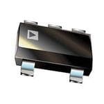
ICGOO电子元器件商城为您提供TMP36GRTZ-REEL7由Analog设计生产,在icgoo商城现货销售,并且可以通过原厂、代理商等渠道进行代购。 TMP36GRTZ-REEL7价格参考¥6.11-¥13.27。AnalogTMP36GRTZ-REEL7封装/规格:温度传感器 - 模拟和数字输出, Temperature Sensor Analog, Local -40°C ~ 125°C 10mV/°C SOT-23-5。您可以下载TMP36GRTZ-REEL7参考资料、Datasheet数据手册功能说明书,资料中有TMP36GRTZ-REEL7 详细功能的应用电路图电压和使用方法及教程。
TMP36GRTZ-REEL7是Analog Devices Inc.推出的一款模拟输出型温度传感器,具有高精度、低功耗和宽工作电压范围等特点。该器件无需外部校准即可提供与温度成比例的电压输出,适用于多种对温度监测有需求的应用场景。

典型应用场景包括:便携式电子设备(如智能手机、平板电脑和可穿戴设备)中的电池温度监控,防止过热;家用电器(如微波炉、电冰箱、热水器等)内部环境温度检测,实现智能温控;工业控制系统中对设备运行温度的实时监测,保障系统稳定运行;此外,还广泛用于环境监测设备、医疗仪器以及汽车电子中的非关键区域温度感知。

TMP36GRTZ-REEL7采用小型化SOT-23-5封装,适合空间受限的高密度电路板设计,并支持卷带包装(REEL7),便于自动化贴片生产,提升制造效率。其工作温度范围通常为-40°C至+125°C,适应严苛环境。由于输出为模拟电压信号,接口简单,可直接连接微控制器的ADC引脚,适用于成本敏感且需要可靠温度测量的中低端应用领域。
| 参数 | 数值 |
| 产品目录 | |
| 描述 | IC SENSOR TEMP 2.7/5.5V SOT23-5板上安装温度传感器 Low VTG Prec Vout 2.7-5.5V |
| 产品分类 | 温度传感器,变送器温度传感器 |
| 品牌 | Analog Devices |
| 产品手册 | |
| 产品图片 |
|
| rohs | 符合RoHS无铅 / 符合限制有害物质指令(RoHS)规范要求 |
| 产品系列 | 板上安装温度传感器,Analog Devices TMP36GRTZ-REEL7- |
| 数据手册 | |
| 产品型号 | TMP36GRTZ-REEL7 |
| 产品目录页面 | |
| 产品种类 | 板上安装温度传感器 |
| 供应商器件封装 | SOT-23-5 |
| 关闭 | Shutdown |
| 其它名称 | TMP36GRTZ-REEL7DKR |
| 准确性 | 3 C |
| 包装 | Digi-Reel® |
| 商标 | Analog Devices |
| 增益 | 10 mV |
| 安装风格 | SMD/SMT |
| 封装 | Reel |
| 封装/外壳 | SC-74A,SOT-753 |
| 封装/箱体 | SOT-23-3 |
| 工厂包装数量 | 3000 |
| 感应温度 | -40°C ~ 125°C |
| 数字输出-总线接口 | 2-Wire |
| 最大工作温度 | + 125 C |
| 最小工作温度 | - 40 C |
| 标准包装 | 1 |
| 电压-电源 | 2.7 V ~ 5.5 V |
| 电源电压-最大 | 5.5 V |
| 电源电压-最小 | 2.7 V |
| 精度 | ±3% |
| 系列 | TMP36 |
| 设备功能 | Temperature Sensor |
| 输出类型 | Analog |


- 商务部:美国ITC正式对集成电路等产品启动337调查
- 曝三星4nm工艺存在良率问题 高通将骁龙8 Gen1或转产台积电
- 太阳诱电将投资9.5亿元在常州建新厂生产MLCC 预计2023年完工
- 英特尔发布欧洲新工厂建设计划 深化IDM 2.0 战略
- 台积电先进制程称霸业界 有大客户加持明年业绩稳了
- 达到5530亿美元!SIA预计今年全球半导体销售额将创下新高
- 英特尔拟将自动驾驶子公司Mobileye上市 估值或超500亿美元
- 三星加码芯片和SET,合并消费电子和移动部门,撤换高东真等 CEO
- 三星电子宣布重大人事变动 还合并消费电子和移动部门
- 海关总署:前11个月进口集成电路产品价值2.52万亿元 增长14.8%


PDF Datasheet 数据手册内容提取
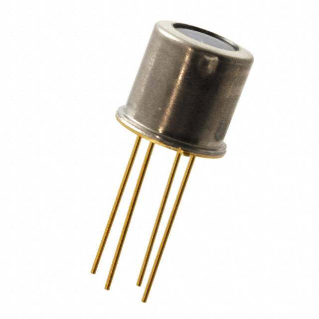
Low Voltage Temperature Sensors Data Sheet TMP35/TMP36/TMP37 FEATURES FUNCTIONAL BLOCK DIAGRAM Low voltage operation (2.7 V to 5.5 V) +VS (2.7V TO 5.5V) Calibrated directly in °C 10 mV/°C scale factor (20 mV/°C on TMP37) TMP35/ ±2°C accuracy over temperature (typ) SHUTDOWN TMP36/ VOUT ±0.5°C linearity (typ) TMP37 SStpaebcliefi ewdit −h4 l0ar°Cge t oc a+p1a2c5it°iCv,e o lpoeardast ion to +150°C 00337-001 Less than 50 µA quiescent current Figure 1. Shutdown current 0.5 µA max Low self-heating PIN CONFIGURATIONS Qualified for automotive applications VOUT 1 5 GND APPLICATIONS Environmental control systems +VS 2 (NToOt Pto V SIEcaWle) Thermal protection IFnirdeu asltarriaml sp rocess control NC N3C = NO CONNECT4 SHUTDOWN 00337-002 Power system monitors Figure 2. RJ-5 (SOT-23) CPU thermal management GENERAL DESCRIPTION VOUT 1 8 +VS NC 2 7 NC TOP VIEW The TMP35/TMP36/TMP37 are low voltage, precision centi- NC 3 (Not to Scale) 6 NC grade temperature sensors. They provide a voltage output that iTsh lien TeaMrlPy 3p5r/oTpMorPti3o6n/aTlM toP t3h7e dCoe nlsoiut sr e(qceunirteig arnady ee)x tteemrnpael rature. GND N4C = NO CONNECT5 SHUTDOWN 00337-003 calibration to provide typical accuracies of ±1°C at +25°C Figure 3. R-8 (SOIC_N) and ±2°C over the −40°C to +125°C temperature range. The low output impedance of the TMP35/TMP36/TMP37 and 1 2 3 its linear output and precise calibration simplify interfacing to BOTTOM VIEW (Not to Scale) temperature control circuitry and ADCs. All three devices are imntuemnd. eTdh efo sru spinplgyl ec-usurrpepnlty r oupnesr wateiolln b ferloomw 520.7 µ VA ,t op r5o.5v iVdi nmga xi- PIN 1, +VS; PIN 2, VOUT; PIN 3, GND 00337-004 Figure 4. T-3 (TO-92) very low self-heating—less than 0.1°C in still air. In addition, a shutdown function is provided to cut the supply current to less than 0.5 µA. The TMP35 is functionally compatible with the LM35/LM45 The TMP37 is intended for applications over the range of 5°C and provides a 250 mV output at 25°C. The TMP35 reads to 100°C and provides an output scale factor of 20 mV/°C. The temperatures from 10°C to 125°C. The TMP36 is specified from TMP37 provides a 500 mV output at 25°C. Operation extends −40°C to +125°C, provides a 750 mV output at 25°C, and to 150°C with reduced accuracy for all devices when operating operates to 125°C from a single 2.7 V supply. The TMP36 is from a 5 V supply. functionally compatible with the LM50. Both the TMP35 and The TMP35/TMP36/TMP37 are available in low cost 3-lead TMP36 have an output scale factor of 10 mV/°C. TO-92, 8-lead SOIC_N, and 5-lead SOT-23 surface-mount packages. Rev. H Document Feedback Information furnished by Analog Devices is believed to be accurate and reliable. However, no responsibility is assumed by Analog Devices for its use, nor for any infringements of patents or other One Technology Way, P.O. Box 9106, Norwood, MA 02062-9106, U.S.A. rights of third parties that may result from its use. Specifications subject to change without notice. No license is granted by implication or otherwise under any patent or patent rights of Analog Devices. Tel: 781.329.4700 ©1996–2015 Analog Devices, Inc. All rights reserved. Trademarks and registered trademarks are the property of their respective owners. Technical Support www.analog.com
TMP35/TMP36/TMP37 Data Sheet TABLE OF CONTENTS Features .............................................................................................. 1 Basic Temperature Sensor Connections .................................. 10 Applications ....................................................................................... 1 Fahrenheit Thermometers ........................................................ 10 General Description ......................................................................... 1 Average and Differential Temperature Measurement ........... 12 Functional Block Diagram .............................................................. 1 Microprocessor Interrupt Generator ....................................... 13 Pin Configurations ........................................................................... 1 Thermocouple Signal Conditioning with Cold-Junction Revision History ............................................................................... 2 Compensation ............................................................................. 14 Specifications ..................................................................................... 3 Using TMP35/TMP36/TMP37 Sensors in Remote Locations ..................................................................................... 15 Absolute Maximum Ratings ............................................................ 4 Temperature to 4–20 mA Loop Transmitter .......................... 15 Thermal Resistance ...................................................................... 4 Temperature-to-Frequency Converter .................................... 16 ESD Caution .................................................................................. 4 Driving Long Cables or Heavy Capacitive Loads .................. 17 Typical Performance Characteristics ............................................. 5 Commentary on Long-Term Stability ..................................... 17 Functional Description .................................................................... 8 Outline Dimensions ....................................................................... 18 Applications Information ................................................................ 9 Ordering Guide .......................................................................... 19 Shutdown Operation .................................................................... 9 Automotive Products ................................................................. 19 Mounting Considerations ........................................................... 9 Thermal Environment Effects .................................................... 9 REVISION HISTORY 5/15—Rev. G to Rev. H 10/02—Rev. B to Rev. C Changed TMP3x to TMP35/TMP36/TMP37 ............ Throughout Changes to Specifications ................................................................. 3 Changes to Figure 28 ...................................................................... 12 Deleted Text from Commentary on Long-Term Stability Changes to Ordering Guide .......................................................... 19 Section .............................................................................................. 13 Updated Outline Dimensions ....................................................... 14 11/13—Rev. F to Rev. G Change to Table 1, Long-Term Stability Parameter ..................... 3 9/01—Rev. A to Rev. B Change to Caption for Figure 38 .................................................. 18 Edits to Specifications ....................................................................... 2 Changes to Ordering Guide .......................................................... 19 Addition of New Figure 1 ................................................................. 2 Deletion of Wafer Test Limits Section ............................................ 3 11/10—Rev. E to Rev. F Changes to Features .......................................................................... 1 6/97—Rev. 0 to Rev. A Updated Outline Dimensions ....................................................... 18 Changes to Ordering Guide .......................................................... 19 3/96—Revision 0: Initial Version Added Automotive Products Section........................................... 20 8/08—Rev. D to Rev. E Updated Outline Dimensions ....................................................... 18 Changes to Ordering Guide .......................................................... 19 3/05—Rev. C to Rev. D Updated Format .................................................................. Universal Changes to Specifications ................................................................ 3 Additions to Absolute Maximum Ratings ..................................... 4 Updated Outline Dimensions ....................................................... 18 Changes to Ordering Guide .......................................................... 19 Rev. H | Page 2 of 19
Data Sheet TMP35/TMP36/TMP37 SPECIFICATIONS V = 2.7 V to 5.5 V, −40°C ≤ T ≤ +125°C, unless otherwise noted. S A Table 1. Parameter1 Symbol Test Conditions/Comments Min Typ Max Unit ACCURACY TMP35/TMP36/TMP37 (F Grade) T = 25°C ±1 ±2 °C A TMP35/TMP36/TMP37 (G Grade) T = 25°C ±1 ±3 °C A TMP35/TMP36/TMP37 (F Grade) Over rated temperature ±2 ±3 °C TMP35/TMP36/TMP37 (G Grade) Over rated temperature ±2 ±4 °C Scale Factor, TMP35 10°C ≤ T ≤ 125°C 10 mV/°C A Scale Factor, TMP36 −40°C ≤ T ≤ +125°C 10 mV/°C A Scale Factor, TMP37 5°C ≤ T ≤ 85°C 20 mV/°C A 5°C ≤ T ≤ 100°C 20 mV/°C A 3.0 V ≤ V ≤ 5.5 V S Load Regulation 0 µA ≤ I ≤ 50 µA L −40°C ≤ T ≤ +105°C 6 20 m°C/µA A −105°C ≤ T ≤ +125°C 25 60 m°C/µA A Power Supply Rejection Ratio PSRR T = 25°C 30 100 m°C/V A 3.0 V ≤ V ≤ 5.5 V 50 m°C/V S Linearity 0.5 °C Long-Term Stability T = 150°C for 1000 hours 0.4 °C A SHUTDOWN Logic High Input Voltage V V = 2.7 V 1.8 V IH S Logic Low Input Voltage V V = 5.5 V 400 mV IL S OUTPUT TMP35 Output Voltage T = 25°C 250 mV A TMP36 Output Voltage T = 25°C 750 mV A TMP37 Output Voltage T = 25°C 500 mV A Output Voltage Range 100 2000 mV Output Load Current I 0 50 µA L Short-Circuit Current I Note 2 250 µA SC Capacitive Load Driving CL No oscillations2 1000 10000 pF Device Turn-On Time Output within ±1°C, 100 kΩ||100 pF load2 0.5 1 ms POWER SUPPLY Supply Range V 2.7 5.5 V S Supply Current I (ON) Unloaded 50 µA SY Supply Current (Shutdown) I (OFF) Unloaded 0.01 0.5 µA SY 1 Does not consider errors caused by self-heating. 2 Guaranteed but not tested. Rev. H | Page 3 of 19
TMP35/TMP36/TMP37 Data Sheet ABSOLUTE MAXIMUM RATINGS Table 2. Stresses at or above those listed under Absolute Maximum Parameter1, 2 Rating Ratings may cause permanent damage to the product. This is a Supply Voltage 7 V stress rating only; functional operation of the product at these Shutdown Pin GND ≤ SHUTDOWN ≤ +VS or any other conditions above those indicated in the operational Output Pin GND ≤ V ≤ +V section of this specification is not implied. Operation beyond OUT S Operating Temperature Range −55°C to +150°C the maximum operating conditions for extended periods may Die Junction Temperature 175°C affect product reliability. Storage Temperature Range −65°C to +160°C THERMAL RESISTANCE IR Reflow Soldering θ is specified for the worst-case conditions, that is, a device in Peak Temperature 220°C (0°C/5°C) JA socket. Time at Peak Temperature Range 10 sec to 20 sec Ramp-Up Rate 3°C/sec Table 3. Thermal Resistance Ramp-Down Rate −6°C/sec Package Type θ θ Unit JA JC Time 25°C to Peak Temperature 6 min TO-92 (T-3-1) 162 120 °C/W IR Reflow Soldering—Pb-Free Package SOIC_N (R-8) 158 43 °C/W Peak Temperature 260°C (0°C) SOT-23 (RJ-5) 300 180 °C/W Time at Peak Temperature Range 20 sec to 40 sec Ramp-Up Rate 3°C/sec Ramp-Down Rate −6°C/sec ESD CAUTION Time 25°C to Peak Temperature 8 min 1 Digital inputs are protected; however, permanent damage can occur on unprotected units from high energy electrostatic fields. Keep units in conductive foam or packaging at all times until ready to use. Use proper antistatic handling procedures. 2 Remove power before inserting or removing units from their sockets. Rev. H | Page 4 of 19
Data Sheet TMP35/TMP36/TMP37 TYPICAL PERFORMANCE CHARACTERISTICS 50 0.4 V) +VS = 3V TO 5.5V, NO LOAD m°C/µA) 40 TION (°C/ 0.3 N ( 30 EC O J ULATI LY RE 0.2 LOAD REG 2100 OWER SUPP 0.1 P 0 00337-005 0 00337-009 –50 0 50 100 150 –50 –25 0 25 50 75 100 125 TEMPERATURE (°C) TEMPERATURE (°C) Figure 5. Load Regulation vs. Temperature (m°C/µA) Figure 8. Power Supply Rejection vs. Temperature 2.0 100.000 a. TMP35 1.8 b. TMP36 c. TMP37 31.600 1.6 +VS = 3V c C/V) V) 1.4 °N (10.000 LTAGE ( 1.2 b EJECTIO 3.160 T VO 1.0 LY R 1.000 U 0.8 P TP a UP 0.320 OU 0.6 R S WE 0.100 0.4 O P 0.20 00337-007 00..003120 00337-010 –50 –25 0 25 50 75 100 125 20 100 1k 10k 100k TEMPERATURE (°C) FREQUENCY (Hz) Figure 6. Output Voltage vs. Temperature Figure 9. Power Supply Rejection vs. Frequency 5 5 4 MINIMUM SUPPLY VOLTAGE REQUIRED TO MEET 3 V) 4 DATA SHEET SPECIFICATION °CY ERROR (C) 210 a abc... MMTYAINPXIIMICMUAUMLM AL LCIMIMCIUTIT R( G(AG CG GYRR AEARDDREE)O)R PPLY VOLTAGE ( 3 NO LOAD b A U R –1 S 2 ACCU –2 b MUM a NI –3 MI 1 ––54 c 00337-008 0 ab.. TTMMPP3357/TMP36 00337-011 0 20 40 60 80 100 120 140 –50 –25 0 25 50 75 100 125 TEMPERATURE (°C) TEMPERATURE (°C) Figure 7. Accuracy Error vs. Temperature Figure 10. Minimum Supply Voltage vs. Temperature Rev. H | Page 5 of 19
TMP35/TMP36/TMP37 Data Sheet 60 400 a. +VS = 5V b. +VS = 3V 50 NT (µA) 40 NO LOAD ME (µs) 300 = +HVIGSH A NTOD SLOHUWT (D3OVW TON P0VIN)S URRE a SE TI 200 C N PLY 30 SPO = +LVOSW A TNOD HSIHGUHT (D0OVW TON P3VIN)S UP RE VOUT SETTLES WITHIN ±1°C S b 100 20 10 00337-012 0 00337-015 –50 –25 0 25 50 75 100 125 –50 –25 0 25 50 75 100 125 TEMPERATURE (°C) TEMPERATURE (°C) Figure 11. Supply Current vs. Temperature Figure 14. VOUT Response Time for +VS Power-Up/Power-Down vs. Temperature 50 400 = SHUTDOWN PIN TA = 25°C, NO LOAD HIGH TO LOW (3V TO 0V) 40 µENT (A) 30 ME (µs) 300 Y CURR ONSE TI 200 UPPL 20 RESP S 100 10 = SHUTDOWN PIN LOW TO HIGH (0V TO 3V) 0 00337-013 0 VOUT SETTLES WITHIN ±1°C 00337-016 0 1 2 3 4 5 6 7 8 –50 –25 0 25 50 75 100 125 SUPPLY VOLTAGE (V) TEMPERATURE (°C) Figure 12. Supply Current vs. Supply Voltage Figure 15. VOUT Response Time for SHUTDOWN Pin vs. Temperature 50 1.0 0.8 40 ab..++VVSS== 53VV 0.6 +TVA S= =2 53°VC T (nA) NO LOAD GE (V) 00..24 SSHIGUNTADLOWN = RREN 30 OLTA 0 U V PLY C 20 TPUT 10..08 P U U O S a 0.6 TA = 25°C 10 0.4 +VS AND SHUTDOWN = SIGNAL 0 b 00337-014 0.02 00337-017 –50 –25 0 25 50 75 100 125 –50 0 50 100 150 200 250 300 350 400 450 TEMPERATURE (°C) TIME (µs) Figure 13. Supply Current vs. Temperature (Shutdown = 0 V) Figure 16. VOUT Response Time to SHUTDOWN Pin and +VS Pin vs. Time Rev. H | Page 6 of 19
Data Sheet TMP35/TMP36/TMP37 110 a 100 10mV 1ms 90 80 b c +VS = 3V, 5V 19000 N %) 70 SIO GE ( 60 DIVI AN 50 LT/ H O C V 40 a. TMP35 SOIC SOLDERED TO 0.5" × 0.3" Cu PCB 30 b. TMP36 SOIC SOLDERED TO 0.6" × 0.4" Cu PCB 10 c. TMP35 TO-92 IN SOCKET SOLDERED TO 0% 20 1" × 0.4" Cu PCB 100 00337-034 00337-019 0 100 200 300 400 500 600 TIME/DIVISION TIME (s) Figure 17. Thermal Response Time in Still Air Figure 20. Temperature Sensor Wideband Output Noise Voltage; Gain = 100, BW = 157 kHz 140 2400 a. TMP35 SOIC SOLDERED TO 0.5" × 0.3" Cu PCB 2200 120 bc . . T1T"MM ×PP 33056.4 TS" OOC-Iu9C 2P S ICNOB LSDOECRKEEDT TSOO L0.D6E" R×E 0D.4 T" OCu PCB V/ Hz)21080000 b NT (s) 100 SITY (n1600 A 80 N1400 T E TIME CONS 6400 b +VS = 3V, 5V AGE NOISE D11208000000 c LT 600 a O 200 a 00337-018 V 4200000 ab.. TTMMPP3357/TMP36 00337-020 0 100 200 300 400 500 600 700 10 100 1k 10k AIR VELOCITY (FPM) FREQUENCY (Hz) Figure 18. Thermal Response Time Constant in Forced Air Figure 21. Voltage Noise Spectral Density vs. Frequency 110 a 100 90 c +VS = 3V, 5V 80 b 70 %) E ( 60 G N A 50 H C 40 a. TMP35 SOIC SOLDERED TO 0.5" × 0.3" Cu PCB 30 b. TMP36 SOIC SOLDERED TO 0.6" × 0.4" Cu PCB c. TMP35 TO-92 IN SOCKET SOLDERED TO 20 1" × 0.4" Cu PCB 100 00337-035 0 10 20 30 40 50 60 TIME (s) Figure 19. Thermal Response Time in Stirred Oil Bath Rev. H | Page 7 of 19
TMP35/TMP36/TMP37 Data Sheet FUNCTIONAL DESCRIPTION An equivalent circuit for the TMP35/TMP36/TMP37 micropower, +VS centigrade temperature sensors is shown in Figure 22. The core SHUTDOWN of the temperature sensor is a band gap core that comprises 25µA transistors Q1 and Q2, biased by Q3 to approximately 8 µA. The band gap core operates both Q1 and Q2 at the same collector 3X 2X current level; however, because the emitter area of Q1 is 10 times that of Q2, the V of Q1 and the V of Q2 are not equal BE BE by the following relationship: Q2 Q4 1X A R1 ∆VBE =VT ×lnAEE,,QQ21 1Q0X1 R3 Resistors R1 and R2 are used to scale this result to produce VOUT R2 the output voltage transfer characteristic of each temperature 7.5µA Q3 sensor and, simultaneously, R2 and R3 are used to scale the V of BE iQn1 t hase aonu topfufste ct htearrmac tiner VisOtiUcTs. Tofa bthlee 4th srueme mtemaripzeersa tthuer ed sifefnerseonrsc.e s GND 6X 2X 00337-006 Figure 22. Temperature Sensor Simplified Equivalent Circuit The output voltage of the temperature sensor is available at the emitter of Q4, which buffers the band gap core and provides load current drive. The current gain of Q4, working with the Table 4. TMP35/TMP36/TMP37 Output Characteristics available base current drive from the previous stage, sets the Offset Output Voltage Output Voltage short-circuit current limit of these devices to 250 µA. Sensor Voltage (V) Scaling (mV/°C) at 25°C (mV) TMP35 0 10 250 TMP36 0.5 10 750 TMP37 0 20 500 Rev. H | Page 8 of 19
Data Sheet TMP35/TMP36/TMP37 APPLICATIONS INFORMATION SHUTDOWN OPERATION THERMAL ENVIRONMENT EFFECTS All TMP35/TMP36/TMP37 devices include a shutdown The thermal environment in which the TMP35/TMP36/TMP37 capability, which reduces the power supply drain to less than sensors are used determines two important characteristics: self- 0.5 µA maximum. This feature, available only in the SOIC_N heating effects and thermal response time. Figure 23 illustrates a and the SOT-23 packages, is TTL/CMOS level-compatible, thermal model of the TMP35/TMP36/TMP37 temperature provided that the temperature sensor supply voltage is equal in sensors, which is useful in under-standing these characteristics. magnitude to the logic supply voltage. Internal to the TMP35/ TJ θJC TC θCA TMP36/TMP37 at the SHUTDOWN pin, a pull-up current source to +V is connected. This allows the SHUTDOWN pin to S be driven from an open-collector/drain driver. A logic low, or PD CCH CC TA zero-volt condition, on the SHUTDOWN pin is required to 00337-021 turn off the output stage. During shutdown, the output of the Figure 23. Thermal Circuit Model temperature sensors becomes high impedance where the potential of the output pin is then determined by external In the T-3 package, the thermal resistance junction-to-case, θJC, circuitry. If the shutdown feature is not used, it is recommended is 120°C/W. The thermal resistance case-to-ambient, CA, is the that the SHUTDOWN pin be connected to +V (Pin 8 on the difference between θJA and θJC, and is determined by the char- S acteristics of the thermal connection. The power dissipation of SOIC_N; Pin 2 on the SOT-23). the temperature sensor, P , is the product of the total voltage D The shutdown response time of these temperature sensors is across the device and its total supply current, including any shown in Figure 14, Figure 15, and Figure 16. current delivered to the load. The rise in die temperature above MOUNTING CONSIDERATIONS the ambient temperature of the medium is given by If the TMP35/TMP36/TMP37 temperature sensors are thermally T = P × (θ + θ ) + T J D JC CA A attached and protected, they can be used in any temperature Thus, the die temperature rise of a TMP35 SOT-23 package measurement application where the maximum temperature mounted into a socket in still air at 25°C and driven from a 5 V range of the medium is between −40°C and +125°C. Properly supply is less than 0.04°C. cemented or glued to the surface of the medium, these sensors The transient response of the TMP35/TMP36/TMP37 sensors are within 0.01°C of the surface temperature. Caution should be to a step change in the temperature is determined by the exercised, especially with T-3 packages, because the leads and thermal resistances and the thermal capacities of the die, C , any wiring to the device can act as heat pipes, introducing CH and the case, C . The thermal capacity of C varies with the errors if the surrounding air-surface interface is not isothermal. C C measurement medium because it includes anything in direct Avoiding this condition is easily achieved by dabbing the leads contact with the package. In all practical cases, the thermal of the temper-ature sensor and the hookup wires with a bead of capacity of C is the limiting factor in the thermal response time thermally conductive epoxy. This ensures that the TMP35/TMP36/ C of the sensor and can be represented by a single-pole RC time TMP37 die temperature is not affected by the surrounding air constant response. Figure 17 and Figure 19 show the thermal temperature. Because plastic IC packaging technology is used, response time of the TMP35/TMP36/TMP37 sensors under excessive mechanical stress should be avoided when fastening the various conditions. The thermal time constant of a temperature device with a clamp or a screw-on heat tab. Thermally conductive sensor is defined as the time required for the sensor to reach epoxy or glue, which must be electrically nonconductive, is 63.2% of the final value for a step change in the temperature. recommended under typical mounting conditions. For example, the thermal time constant of a TMP35 SOIC These temperature sensors, as well as any associated circuitry, package sensor mounted onto a 0.5" × 0.3" PCB is less than should be kept insulated and dry to avoid leakage and corrosion. 50 sec in air, whereas in a stirred oil bath, the time constant is In wet or corrosive environments, any electrically isolated metal less than 3 sec. or ceramic well can be used to shield the temperature sensors. Condensation at very cold temperatures can cause errors and should be avoided by sealing the device, using electrically non- conductive epoxy paints or dip or any one of the many printed circuit board coatings and varnishes. Rev. H | Page 9 of 19
TMP35/TMP36/TMP37 Data Sheet BASIC TEMPERATURE SENSOR CONNECTIONS FAHRENHEIT THERMOMETERS Figure 24 illustrates the basic circuit configuration for the Although the TMP35/TMP36/TMP37 temperature sensors are TMP35/TMP36/TMP37 temperature sensors. The table in centigrade temperature sensors, a few components can be used Figure 24 shows the pin assignments of the temperature sensors to convert the output voltage and transfer characteristics to for the three package types. For the SOT-23, Pin 3 is labeled NC, directly read Fahrenheit temperatures. Figure 25 shows an as are Pin 2, Pin 3, Pin 6, and Pin 7 on the SOIC_N package. It example of a simple Fahrenheit thermometer using either the is recommended that no electrical connections be made to these TMP35 or the TMP37. Using the TMP35, this circuit can be pins. If the shutdown feature is not needed on the SOT-23 or on used to sense temperatures from 41°F to 257°F with an output the SOIC_N package, the SHUTDOWN pin should be transfer characteristic of 1 mV/°F; using the TMP37, this circuit connected to +V. can be used to sense temperatures from 41°F to 212°F with an S 2.7V < +VS < 5.5V output transfer characteristic of 2 mV/°F. This particular approach does not lend itself to the TMP36 because of its 0.1µF inherent 0.5 V output offset. The circuit is constructed with an AD589, a 1.23 V voltage reference, and four resistors whose +VS values for each sensor are shown in the table in Figure 25. The SHUTDOWN TMP3x VOUT scaling of the output resistance levels ensures minimum output GND loading on the temp-erature sensors. A generalized expression for the transfer equation of the circuit is given by PIN ASSIGNMENTS V = R1 (TMP35)+ R3 (AD589) PACKAGE +VS GND VOUT SHUTDOWN OUT R1+R2 R3+R4 SSTOOO-ITC9-22_3N 821 453 112 N54A 00337-022 wTMhePre3:5 is the output voltage of the TMP35 or the TMP37 at the Figure 24. Basic Temperature Sensor Circuit Configuration measurement temperature, TM. AD589 is the output voltage of the reference, that is, 1.23 V. Note the 0.1 µF bypass capacitor on the input. This capacitor The output voltage of this circuit is not referenced to the should be a ceramic type, have very short leads (surface-mount circuit’s common ground. If this output voltage were applied is preferable), and be located as close as possible in physical directly to the input of an ADC, the ADC common ground proximity to the temperature sensor supply pin. Because these should be adjusted accordingly. temperature sensors operate on very little supply current and may be exposed to very hostile electrical environments, it is +VS important to minimize the effects of radio frequency interference 0.1µF (RFI) on these devices. The effect of RFI on these temperature +VS sensors specifically and on analog ICs in general is manifested as TMP35/ VOUT abnormal dc shifts in the output voltage due to the rectification TMP37 R1 of the high frequency ambient noise by the IC. When the GND + devices are operated in the presence of high frequency radiated or conducted noise, a large value tantalum capacitor (±2.2 µF) R2 placed across the 0.1 µF ceramic capacitor may offer additional VOUT noise immunity. AD589 R3 1.23V – R4 SENSOR TCVOUT R1 (kΩ) R2 (kΩ) R3 (kΩ) R4 (kΩ) TTMMPP3375 12mmVV//°°FF 4455..33 1100 1100 317842 00337-023 Figure 25. TMP35/TMP37 Fahrenheit Thermometers Rev. H | Page 10 of 19
Data Sheet TMP35/TMP36/TMP37 The same circuit principles can be applied to the TMP36, but At the expense of additional circuitry, the offset produced by because of the inherent offset of the TMP36, the circuit uses only the circuit in Figure 26 can be avoided by using the circuit in two resistors, as shown in Figure 26. In this circuit, the output Figure 27. In this circuit, the output of the TMP36 is conditioned voltage transfer characteristic is 1 mV/°F but is referenced to by a single-supply, micropower op amp, the OP193. Although the common ground of the circuit; however, there is a 58 mV the entire circuit operates from a single 3 V supply, the output (58°F) offset in the output voltage. For example, the output voltage of the circuit reads the temperature directly, with a voltage of the circuit reads 18 mV if the TMP36 is placed in a transfer characteristic of 1 mV/°F, without offset. This is accom- −40°F ambient environment and 315 mV at +257°F. plished through an ADM660, which is a supply voltage inverter. +VS The 3 V supply is inverted and applied to the V− terminal of the OP193. Thus, for a temperature range between −40°F and +257°F, +VS the output of the circuit reads −40 mV to +257 mV. A general VOUT expression for the transfer equation of the circuit is given by 0.1µF TMP36 GND R451.3kΩ VOUT =R5R+6R61+ RR34 (TMP36)−RR43V2S VOUT @ 1mV/°F–58°F R2 10kΩ VVOOUUTT @@ –+4205°7F°F = = 1 83m15VmV 00337-024 Figure 26. TMP36 Fahrenheit Thermometer Version 1 +3V R1 50kΩ R3 R4 R2 C1+ 0.1µF 50kΩ 10µF 7 2 +VS – OP193 VOUT @ 1mV/°F + VOUT R5 3 6 –40°F ≤ TA ≤ +257°F 10µF/0.1µF TMP36 + R6 4 GND 8 1 5 NC –3V ELEMENT VALUE 2 10µF + R3 258.6kΩ + ADM660 6 R4 10kΩ 10µF 4 NC R5 47.7kΩ 3 7 R6 10kΩ 00337-025 Figure 27. TMP36 Fahrenheit Thermometer Version 2 Rev. H | Page 11 of 19
TMP35/TMP36/TMP37 Data Sheet AVERAGE AND DIFFERENTIAL TEMPERATURE 2.7V < +VS < 5.5V MEASUREMENT 0.1µF VTEMP(AVG) In many commercial and industrial environments, temperature 7 @ 10mV/°C FOR TMP35/TMP36 sensors often measure the average temperature in a building, or 3 + @ 20mV/°C FOR TMP37 6 the difference in temperature between two locations on a factory OP193 2 – floor or in an industrial process. The circuits in Figure 28 and 4 R5 Figure 29 demonstrate an inexpensive approach to average and 100kΩ R1 differential temperature measurement. 300kΩ TMP3x In Figure 28, an OP193 sums the outputs of three temperature sensors to produce an output voltage scaled by 10 mV/°C that R6 7.5kΩ represents the average temperature at three locations. The circuit R2 300kΩ can be extended to include as many temperature sensors as TMP3x required as long as the transfer equation of the circuit is FOR R1 = R2 = R3 = R; maintained. In this application, it is recommended that one VTEMP(AVG) = 1 (TMP3x1 + TMP3x2 + TMP3x3) R3 3 temperature sensor type be used throughout the circuit; 300kΩ R5 =R1 TMP3x 3 otherwise, the output voltage of the circuit cannot produce an R4 R4 = R6 accurate reading of the various ambient conditions. 7.5kΩ The circuit in Figure 29 illustrates how a pair of TMP35/TMP36/ 00337-026 TMP37 sensors used with an OP193 configured as a difference Figure 28. Configuring Multiple Sensors for amplifier can read the difference in temperature between two Average Temperature Measurements locations. In these applications, it is always possible that one 2.7V < +VS < 5.5V temperature sensor is reading a temperature below that of the other sensor. To accommodate this condition, the output of the OP193 is offset to a voltage at one-half the supply via R5 and R6. Thus, the output voltage of the circuit is measured relative R11 R21 to this point, as shown in Figure 29. Using the TMP36, the 0.1µF TM@ PT136 R8 output voltage of the circuit is scaled by 10 mV/°C. To minimize 25kΩ the error in the difference between the two measured temperatures, a common, readily available thin-film resistor network is used for R1 to R4. 0.1µF 7 2 –OP193 6 VOUT 0.1µF TMP36 R31 3 + @ T2 4 R9 R7 25kΩ 100kΩ CENTERED AT R41 1µF 0°C ≤ TA ≤ 125°C 10R05kΩ 10R06kΩ VOUT = T2 – T1 @ 10mV/°C CENTERED AT VS 2 NO1TRE:1–R4, CADDOCK T914–100k–100, OR EQUIVALENT. 00337-027 Figure 29. Configuring Multiple Sensors for Differential Temperature Measurements Rev. H | Page 12 of 19
Data Sheet TMP35/TMP36/TMP37 MICROPROCESSOR INTERRUPT GENERATOR Because temperature is a slowly moving quantity, the possibility for comparator chatter exists. To avoid this condition, hysteresis These inexpensive temperature sensors can be used with a is used around the comparator. In this application, a hysteresis voltage reference and an analog comparator to configure an of 5°C about the trip point was arbitrarily chosen; the ultimate interrupt generator for microprocessor applications. With the value for hysteresis should be determined by the end application. popularity of fast microprocessors, the need to indicate a The output logic voltage swing of the comparator with R1 and microprocessor overtemperature condition has grown R2 determines the amount of comparator hysteresis. Using a tremendously. The circuit in Figure 30 demonstrates one way to 3.3 V supply, the output logic voltage swing of the CMP402 is generate an interrupt using a TMP35, a CMP402 analog 2.6 V; therefore, for a hysteresis of 5°C (50 mV at 10 mV/°C), comparator, and a REF191, a 2 V precision voltage reference. R1 is set to 20 kΩ, and R2 is set to 1 MΩ. An expression for the The circuit is designed to produce a logic high interrupt signal hysteresis of this circuit is given by if the microprocessor temperature exceeds 80°C. This 80°C trip R1( ) point was arbitrarily chosen (final value set by the microprocessor V = V HYS R2 LOGICSWING,CMP402 thermal reference design) and is set using an R3 to R4 voltage divider of the REF191 output voltage. Because the output of the Because this circuit is probably used in close proximity to high TMP35 is scaled by 10 mV/°C, the voltage at the inverting speed digital circuits, R1 is split into equal values and a 1000 pF terminal of the CMP402 is set to 0.8 V. capacitor is used to form a low-pass filter on the output of the TMP35. Furthermore, to prevent high frequency noise from contaminating the comparator trip point, a 0.1 µF capacitor is used across R4. 3.3V R2 1MΩ +VS 0.1µF R1A R1B 3 0.1µF TMP35 VOUT 10kΩ 10kΩ 6 – 4 2 R1050kΩ C10L00pF 5 +CMP402 14 INTERRUPT GND 0.1µF >80°C 2 13 <80°C R3 6 16kΩ VREF REF191 3 + R4 4 1µF 10kΩ 0.1µF C1 = 14 CMP402 00337-028 Figure 30. Microprocessor Overtemperature Interrupt Generator Rev. H | Page 13 of 19
TMP35/TMP36/TMP37 Data Sheet THERMOCOUPLE SIGNAL CONDITIONING WITH and the wires of the thermocouple from introducing an error in COLD-JUNCTION COMPENSATION the measured temperature. This compensation works extremely well for circuit ambient temperatures in the range of 20°C to 50°C. The circuit in Figure 31 conditions the output of a Type K Over a 250°C measurement temperature range, the thermocouple thermocouple, while providing cold-junction compensation for produces an output voltage change of 10.151 mV. Because the temperatures between 0°C and 250°C. The circuit operates from required output full-scale voltage of the circuit is 2.5 V, the gain a single 3.3 V to 5.5 V supply and is designed to produce an of the circuit is set to 246.3. Choosing R4 equal to 4.99 kΩ sets output voltage transfer characteristic of 10 mV/°C. R5 equal to 1.22 MΩ. Because the closest 1% value for R5 is A Type K thermocouple exhibits a Seebeck coefficient of 1.21 MΩ, a 50 kΩ potentiometer is used with R5 for fine trim of approximately 41 µV/°C; therefore, at the cold junction, the the full-scale output voltage. Although the OP193 is a superior TMP35, with a temperature coefficient of 10 mV/°C, is used single-supply, micropower operational amplifier, its output stage with R1 and R2 to introduce an opposing cold-junction temp- is not rail-to-rail; therefore, the 0°C output voltage level is 0.1 V. erature coefficient of −41 µV/°C. This prevents the isothermal, If this circuit is digitized by a single-supply ADC, the ADC cold-junction connection between the PCB tracks of the circuit common should be adjusted to 0.1 V accordingly. 3.3V < +VS < 5.5V +VS P1 50kΩ 0.1µF TMP35 VOUT R150%3MΩ 4.9R94kΩ 1.2R15M1Ω 0.1µF GND R11 24.9kΩ 7 2 – OP193 6 VOUT CU 0V TO 2.5V CHROMEL 3 R6 + + 100kΩ 4 5% TYPE K THERMO- COLD COUPLE JUNCTION ALUMEL CU NOTE: – 1ALL RESISTORS 1% UNLESS OTHERWISE NOTED. R21 0°C ≤ TA ≤ 250°C ISOBTLHOECRKMAL 102Ω 00337-029 Figure 31. Single-Supply, Type K Thermocouple Signal Conditioning Circuit with Cold-Junction Compensation Rev. H | Page 14 of 19
Data Sheet TMP35/TMP36/TMP37 USING TMP35/TMP36/TMP37 SENSORS IN TEMPERATURE TO 4–20 mA LOOP TRANSMITTER REMOTE LOCATIONS In many process control applications, 2-wire transmitters are In many industrial environments, sensors are required to used to convey analog signals through noisy ambient environ- operate in the presence of high ambient noise. These noise ments. These current transmitters use a zero-scale signal current sources take many forms, for example, SCR transients, relays, of 4 mA, which can be used to power the signal conditioning radio transmitters, arc welders, and ac motors. They can also circuitry of the transmitter. The full-scale output signal in these be used at considerable distances from the signal conditioning transmitters is 20 mA. circuitry. These high noise environments are typically in the Figure 33 illustrates a circuit that transmits temperature inform- form of electric fields, so the voltage output of the temperature ation in this fashion. Using a TMP35/TMP36/TMP37 as the sensor can be susceptible to contamination from these noise temperature sensor, the output current is linearly proportional sources. to the temperature of the medium. The entire circuit operates Figure 32 illustrates a way to convert the output voltage of a from the 3 V output of the REF193. The REF193 requires no TMP35/TMP36/TMP37 sensor into a current to be transmitted external trimming because of its tight initial output voltage down a long twisted pair shielded cable to a ground referenced tolerance and the low supply current of the TMP35/TMP36/ receiver. The temperature sensors are not capable of high output TMP37, the OP193, and the REF193. The entire circuit consumes current operation; thus, a standard PNP transistor is used to less than 3 mA from a total budget of 4 mA. The OP193 regulates boost the output current drive of the circuit. As shown in the the output current to satisfy the current summation at the table in Figure 32, the values of R2 and R3 were chosen to noninverting node of the OP193. A generalized expression for produce an arbitrary full-scale output current of 2 mA. Lower the KCL equation at Pin 3 of the OP193 is given by values for the full-scale current are not recommended. The minimum-scale output current produced by the circuit could be IOUT =R17×TMPR3x1×R3+VRERF2×R3 contaminated by ambient magnetic fields operating in the near vicinity of the circuit/cable pair. Because the circuit uses an For each temperature sensor, Table 5 provides the values for the external transistor, the minimum recommended operating components P1, P2, and R1 to R4. voltage for this circuit is 5 V. To minimize the effects of EMI (or Table 5. Circuit Element Values for Loop Transmitter RFI), both the circuit and the temperature sensor supply pins Sensor R1 P1 R2 P2 R3 R4 are bypassed with good quality ceramic capacitors. TMP35 97.6 kΩ 5 kΩ 1.58 MΩ 100 kΩ 140 kΩ 56.2 kΩ TMP36 97.6 kΩ 5 kΩ 931 kΩ 50 kΩ 97.6 kΩ 47 kΩ TMP37 97.6 kΩ 5 kΩ 10.5 kΩ 500 Ω 84.5 kΩ 8.45 kΩ R1 4.7kΩ 5V The 4 mA offset trim is provided by P2, and P1 provides the 2N2907 VOUT full-scale gain trim of the circuit at 20 mA. These two trims do 0.1µF +VS not interact because the noninverting input of the OP193 is R3 held at a virtual ground. The zero-scale and full-scale output 0.01µF TMP3x VOUT currents of the circuit are adjusted according to the operating temperature range of each temperature sensor. The Schottky GND R2 diode, D1, is required in this circuit to prevent loop supply TWISTED PAIR power-on transients from pulling the noninverting input of the BELDEN TYPE 9502 OR EQUIVALENT OP193 more than 300 mV below its inverting input. Without SENSOR R2 R3 this diode, such transients can cause phase reversal of the TMP35 634 634 TTMMPP3367 18k87 18k87 00337-030 Topheer laotioopn saul papmlyp lvifoiletra gaen dco pmospsliibalnec lea tocfh t-huep c oirfc tuhiet itsr alinmsmiteitdt ebry. Figure 32. Remote, 2-Wire Boosted Output Current Temperature Sensor the maximum applied input voltage to the REF193; it is from 9 V to 18 V. Rev. H | Page 15 of 19
TMP35/TMP36/TMP37 Data Sheet 3V 6 2 REF193 + R21 1µF 4 VLOOP 9V TO 18V P21 4mA +VS ADJUST 0.1µF TMP3x VOUTR11 2P0m11A 23 –OP1793 6 10R06kΩ Q2N11711 GND ADJUST + 4 VOUT D1 R5 R31 R41 100kΩ RL 250Ω R7 100Ω NOTE: D1: HP5082-2810 1SEE TEXT FOR VALUES. IL 00337-032 Figure 33. Temperature to 4–20 mA Loop Transmitter TEMPERATURE-TO-FREQUENCY CONVERTER Another common method of transmitting analog information 5V from a remote location is to convert a voltage to an equivalent value in the frequency domain. This is readily done with any of 0.1µF CT1 the low cost, monolithic voltage-to-frequency converters (VFCs) +VS R5kPΩU available. These VFCs feature a robust, open-collector output 8 6 7 transistor for easy interfacing to digital circuitry. The digital 10µF/0.1µF TMP3x VOUT 4 1 signal produced by the VFC is less susceptible to contamination 3 AD654 fOUT from external noise sources and line voltage drops because the GND 5 2 only important information is the frequency of the digital sig- R1 nal. When the conversions between temperature and frequency RT1 5V NB: ATTA (MIN),fOUT = 0Hz are done accurately, the temperature data from the sensors can P1 f NOTE: be reliably transmitted. P2 OFOFUSTET 1RT AND CT – SEE TABLE The circuit in Figure 34 illustrates a method by which the 100kΩ R4O70FΩF1 ROFF2 10Ω outputs of these temperature sensors can be converted to a frequency using the AD654. The output signal of the AD654 is a square wave that is proportional to the dc input voltage across SENSOR RT (R1 + P1) CT TMP35 11.8kΩ + 500Ω 1.7nF Pin 4 and Pin V3. The tVransfer equation of the circuit is given by TTMMPP3367 1186..22kkΩΩ ++ 15k0Ω0Ω 12..81nnFF 00337-031 f TPM OFFSET Figure 34. Temperature-to-Frequency Converter OUT 10(RT CT) Rev. H | Page 16 of 19
Data Sheet TMP35/TMP36/TMP37 An offset trim network (f OFFSET ) is included with this COMMENTARY ON LONG-TERM STABILITY OUT circuit to set f to 0 Hz when the minimum output voltage of OUT The concept of long-term stability has been used for many years the temperature sensor is reached. Potentiometer P1 is required to describe the amount of parameter shift that occurs during to calibrate the absolute accuracy of the AD654. The table in the lifetime of an IC. This is a concept that has been typically Figure 34 illustrates the circuit element values for each of the applied to both voltage references and monolithic temperature three sensors. The nominal offset voltage required for 0 Hz sensors. Unfortunately, integrated circuits cannot be evaluated output from the TMP35 is 50 mV; for the TMP36 and TMP37, at room temperature (25°C) for 10 years or more to determine the offset voltage required is 100 mV. For the circuit values this shift. As a result, manufacturers very typically perform shown, the output frequency transfer characteristic of the accelerated lifetime testing of integrated circuits by operating circuit was set at 50 Hz/°C in all cases. At the receiving end, a ICs at elevated temperatures (between 125°C and 150°C) over a frequency-to-voltage converter (FVC) can be used to convert shorter period of time (typically, between 500 and 1000 hours). the frequency back to a dc voltage for further processing. One As a result of this operation, the lifetime of an integrated circuit such FVC is the AD650. is significantly accelerated due to the increase in rates of reaction For complete information about the AD650 and the AD654, within the semiconductor material. consult the individual data sheets for those devices. DRIVING LONG CABLES OR HEAVY CAPACITIVE LOADS Although the TMP35/TMP36/TMP37 temperature sensors can drive capacitive loads up to 10,000 pF without oscillation, output voltage transient response times can be improved by using a small resistor in series with the output of the temperature sensor, as shown in Figure 35. As an added benefit, this resistor forms a low-pass filter with the cable capacitance, which helps to reduce bandwidth noise. Because the temperature sensor is likely to be used in environments where the ambient noise level can be very high, this resistor helps to prevent rectification by the devices of the high frequency noise. The combination of this resistor and the supply bypass capacitor offers the best protection. +VS 0.1µF TMP3x VOUT 750Ω LONG CABLE OR HEAVY CAPACITIVE LOADS GND 00337-033 Figure 35. Driving Long Cables or Heavy Capacitive Loads Rev. H | Page 17 of 19
TMP35/TMP36/TMP37 Data Sheet OUTLINE DIMENSIONS 5.00(0.1968) 4.80(0.1890) 8 5 4.00(0.1574) 6.20(0.2441) 3.80(0.1497) 1 4 5.80(0.2284) 1.27(0.0500) 0.50(0.0196) BSC 1.75(0.0688) 0.25(0.0099) 45° 0.25(0.0098) 1.35(0.0532) 8° 0.10(0.0040) 0° COPLANARITY 0.51(0.0201) 0.10 SEATING 0.31(0.0122) 0.25(0.0098) 10..2470((00..00510507)) PLANE 0.17(0.0067) COMPLIANTTOJEDECSTANDARDSMS-012-AA C(RINOEFNPEATRRREOENNLCLTEIHNEOGSNDELISYM)AEANNRDSEIAORRNOESUNANORDETEDAIN-POMPFRIFLOLMPIMIRLELIATIMTEEERTFSEO;RIRNECUQHSUEDIVIINMAELDENENSSTIIOGSNNFS.OR 012407-A Figure 36. 8-Lead Standard Small Outline Package [SOIC_N] Narrow Body (R-8) Dimensions shown in millimeters and (inches) 3.00 2.90 2.80 1.70 5 4 3.00 1.60 2.80 1.50 2.60 1 2 3 0.95BSC 1.90 BSC 1.30 1.15 0.90 1.45MAX 0.20MAX 0.95MIN 0.08MIN 0.55 0.15MAX 10° 0.45 0.05MIN 0.50MAX SPELAATNIENG 5° B0S.6C0 0.35 0.35MIN 0° COMPLIANTTOJEDECSTANDARDSMO-178-AA 11-01-2010-A Figure 37. 5-Lead Small Outline Transistor Package [SOT-23] (RJ-5) Dimensions shown in millimeters Rev. H | Page 18 of 19
Data Sheet TMP35/TMP36/TMP37 0.165 (4.19) 0.210 (5.33) 0.145 (3.68) 0.190 (4.83) 0.125 (3.18) 0.170 (4.32) 00..00212805 ((00..5467)) 0.055 (1.40) 00..10915705 ((22..9428)) 0.0150 (0.38) 0.050 (1.27) 0.0800 (2.03) 0.045 (1.15) 3 0.205 (5.21) 0.190 (4.83) 2 0.175 (4.45) 0.105 (2.68) 1 0.100 (2.54) 0.020 (0.51) FRONT VIEW 0.500 (12.70) MIN 0.095 (2.42) 0.017 (0.43) 0.014 (0.36) SEATING BOTTOM VIEW PLANE COMPLIANT TO JEDEC STANDARDS TO-226-AA C(RINEO FNPETARRREOENLNCLTEIHN EOGSN DELISYM) AEANNRSDEI OARRNOESU NNADOREETD IAN-OP IPFNRFC OHEPEQRSUI;AI VMTAIELL LEFIONMTRES TU EFSORE R DINIM DEENSSIGIONN.S 042208-A Figure 38. 3-Pin Plastic Header-Style Package [TO-92] (T-3-1) Dimensions shown in inches and (millimeters) ORDERING GUIDE Accuracy at Linear Operating Package Model1, 2 25°C (°C max) Temperature Range Package Description Option Branding TMP35FSZ-REEL ±2.0 10°C to 125°C 8-Lead Standard Small Outline Package (SOIC_N) R-8 TMP35GRTZ-REEL7 ±3.0 10°C to 125°C 5-Lead Small Outline Transistor Package (SOT-23) RJ-5 #T11 TMP35GT9Z ±3.0 10°C to 125°C 3-Pin Plastic Header-Style Package (TO-92) T-3-1 ADW75001Z-0REEL7 ±3.0 −40°C to +125°C 5-Lead Small Outline Transistor Package (SOT-23) RJ-5 #T6G TMP36FS ±2.0 −40°C to +125°C 8-Lead Standard Small Outline Package (SOIC_N) R-8 TMP36FS-REEL ±2.0 −40°C to +125°C 8-Lead Standard Small Outline Package (SOIC_N) R-8 TMP36FSZ ±2.0 −40°C to +125°C 8-Lead Standard Small Outline Package (SOIC_N) R-8 TMP36FSZ-REEL ±2.0 −40°C to +125°C 8-Lead Standard Small Outline Package (SOIC_N) R-8 TMP36GRT-REEL7 ±3.0 −40°C to +125°C 5-Lead Small Outline Transistor Package (SOT-23) RJ-5 T6G TMP36GRTZ-REEL7 ±3.0 −40°C to +125°C 5-Lead Small Outline Transistor Package (SOT-23) RJ-5 #T6G TMP36GSZ ±3.0 −40°C to +125°C 8-Lead Standard Small Outline Package (SOIC_N) R-8 TMP36GSZ-REEL ±3.0 −40°C to +125°C 8-Lead Standard Small Outline Package (SOIC_N) R-8 TMP36GSZ-REEL7 ±3.0 −40°C to +125°C 8-Lead Standard Small Outline Package (SOIC_N) R-8 TMP36GT9 ±3.0 −40°C to +125°C 3-Pin Plastic Header-Style Package (TO-92) T-3-1 TMP36GT9Z ±3.0 −40°C to +125°C 3-Pin Plastic Header-Style Package (TO-92) T-3-1 TMP36-PT7 −40°C to +125°C Chips or Die TMP37FT9Z ±2.0 5°C to 100°C 3-Pin Plastic Header-Style Package (TO-92) T-3-1 TMP37GRTZ-REEL7 ±3.0 5°C to 100°C 5-Lead Small Outline Transistor Package (SOT-23) RJ-5 #T12 1 Z = RoHS Compliant Part. 2 W = Qualified for Automotive Applications. AUTOMOTIVE PRODUCTS The ADW75001Z-0REEL7 model is available with controlled manufacturing to support the quality and reliability requirements of automotive applications. Note that this automotive model may have specifications that differ from the commercial models; therefore, designers should review the Specifications section of this data sheet carefully. Only automotive grade products shown are available for use in automotive applications. Contact your local Analog Devices account representative for specific product ordering information and to obtain the specific Automotive Reliability reports for these models. ©1996–2015 Analog Devices, Inc. All rights reserved. Trademarks and registered trademarks are the property of their respective owners. D00337-0-5/15(H) Rev. H | Page 19 of 19
Mouser Electronics Authorized Distributor Click to View Pricing, Inventory, Delivery & Lifecycle Information: A nalog Devices Inc.: TMP36FSZ TMP35GT9Z TMP36GSZ-REEL TMP36GT9Z TMP37FT9Z TMP36GT9 TMP36GSZ-REEL7 TMP36GRTZ-REEL7 TMP35GRTZ-REEL7 TMP36FS TMP37GRTZ-REEL7 TMP36-PT7 TMP36GSZ TMP36FSZ- REEL TMP36FS-REEL TMP36GRT-REEL7 TMP35FSZ-REEL ADW75001Z-0REEL7