ICGOO在线商城 > 传感器,变送器 > 温度传感器 - 模拟和数字输出 > LTC2997CDCB#TRMPBF

 Datasheet下载
- 型号: LTC2997CDCB#TRMPBF
- 制造商: LINEAR TECHNOLOGY
- 库位|库存: xxxx|xxxx
- 要求:
| 数量阶梯 | 香港交货 | 国内含税 |
| +xxxx | $xxxx | ¥xxxx |
查看当月历史价格
查看今年历史价格
LTC2997CDCB#TRMPBF产品简介:
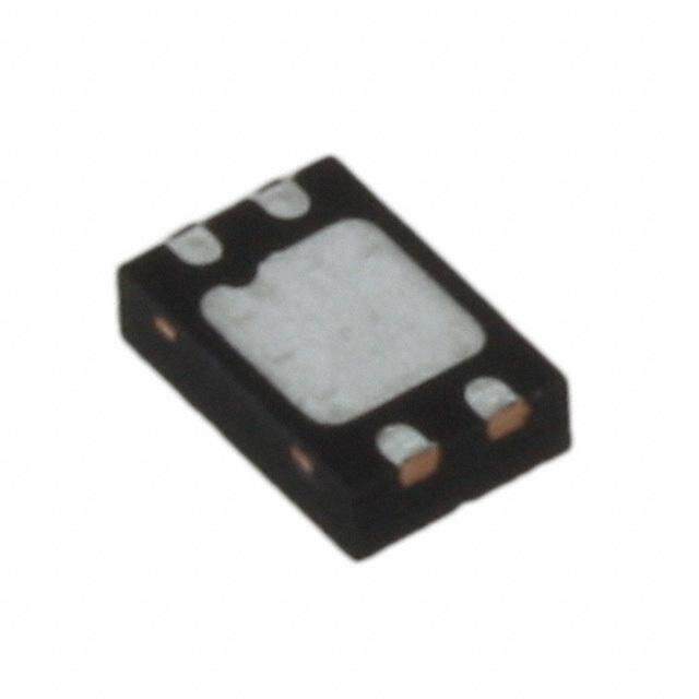
ICGOO电子元器件商城为您提供LTC2997CDCB#TRMPBF由LINEAR TECHNOLOGY设计生产,在icgoo商城现货销售,并且可以通过原厂、代理商等渠道进行代购。 LTC2997CDCB#TRMPBF价格参考。LINEAR TECHNOLOGYLTC2997CDCB#TRMPBF封装/规格:温度传感器 - 模拟和数字输出, 温度传感器 模拟,本地/远程 0°C ~ 70°C 4mV/°C 6-DFN(2x3)。您可以下载LTC2997CDCB#TRMPBF参考资料、Datasheet数据手册功能说明书,资料中有LTC2997CDCB#TRMPBF 详细功能的应用电路图电压和使用方法及教程。
LTC2997CDCB#TRMPBF 是 Linear Technology(现为 Analog Devices 旗下品牌)生产的一款温度传感器,属于“温度传感器 - 模拟和数字输出”类别。它集成了高精度的温度测量功能,并支持模拟和数字输出,适合多种应用场景。以下是其主要应用场景:

 1. 工业控制
   - 在工业自动化系统中,LTC2997 可用于监测设备或环境温度,确保关键设备在安全温度范围内运行。
   - 应用于电机驱动、电源模块和热管理系统,提供实时温度反馈以优化性能。

 2. 通信设备
   - 在基站、路由器和其他通信设备中,LTC2997 可监控内部组件(如功率放大器、处理器等)的温度,防止过热导致故障。
   - 提供精确的温度数据,用于动态调整散热风扇速度或降低功耗。

 3. 消费电子产品
   - 用于笔记本电脑、平板电脑和智能手机中的温度监控,保护电池和处理器免受高温损害。
   - 支持智能温控功能,例如根据温度调节充电速率或屏幕亮度。

 4. 医疗设备
   - 在医疗仪器(如体温计、血液分析仪等)中,LTC2997 提供高精度的温度测量,满足严格的医疗标准。
   - 适用于需要实时温度监控的场景,例如恒温培养箱或冷藏设备。

 5. 汽车电子
   - 用于电动汽车电池管理系统(BMS),监测电池组温度,防止过热或过冷影响电池寿命。
   - 应用于发动机舱或动力系统中,确保关键部件在正常工作温度范围内。

 6. 数据中心与服务器
   - 监控服务器机房内的温度分布,优化空调和散热系统的运行效率。
   - 提供报警功能,当温度超过预设阈值时触发保护机制。

 7. 航空航天与国防
   - 在极端环境下(如卫星、无人机等),LTC2997 的高精度和可靠性使其成为理想选择。
   - 用于监控关键电子组件的温度,确保系统稳定运行。

 特点总结:
- 高精度温度测量(典型误差 ±0.5°C)。
- 支持模拟和数字输出,便于集成到不同系统中。
- 小型封装(如 MSOP 或 QFN),适合空间受限的应用。
- 低功耗设计,适合电池供电设备。

LTC2997CDCB#TRMPBF 凭借其出色的性能和灵活性,广泛应用于对温度敏感的各类场景中,帮助实现高效、可靠的温度管理。
| 参数 | 数值 |
| 产品目录 | 集成电路 (IC) |
| 描述 | IC SENSOR THERMAL 6DFN |
| 产品分类 | |
| 品牌 | Linear Technology |
| 数据手册 | http://www.linear.com/docs/40023 |
| 产品图片 |
|
| 产品型号 | LTC2997CDCB#TRMPBF |
| rohs | 无铅 / 符合限制有害物质指令(RoHS)规范要求 |
| 产品系列 | - |
| 传感器类型 | 内部和外部 |
| 供应商器件封装 | 6-DFN(2x3) |
| 其它名称 | LTC2997CDCB#TRMPBFDKR |
| 功能 | 温度监控系统(传感器) |
| 包装 | Digi-Reel® |
| 安装类型 | 表面贴装 |
| 封装/外壳 | 6-WFDFN 裸露焊盘 |
| 工作温度 | 0°C ~ 70°C |
| 感应温度 | 0°C ~ 70°C, -40°C ~ 125°C |
| 拓扑 | 比较器,多路复用器,电压基准 |
| 标准包装 | 1 |
| 特色产品 | http://www.digikey.cn/product-highlights/zh/ltc2997-remoteinternal-temperature-sensor/52601 |
| 电压-电源 | 2.5 V ~ 5.5 V |
| 精度 | ±1.5°C 本地(最大), ±1.5°C 远程(最大) |
| 输出报警 | 无 |
| 输出类型 | 模拟电压 |
| 输出风扇 | 无 |
| 配用 | /product-detail/zh/DC1767A/DC1767A-ND/2962539 |


- 商务部:美国ITC正式对集成电路等产品启动337调查
- 曝三星4nm工艺存在良率问题 高通将骁龙8 Gen1或转产台积电
- 太阳诱电将投资9.5亿元在常州建新厂生产MLCC 预计2023年完工
- 英特尔发布欧洲新工厂建设计划 深化IDM 2.0 战略
- 台积电先进制程称霸业界 有大客户加持明年业绩稳了
- 达到5530亿美元!SIA预计今年全球半导体销售额将创下新高
- 英特尔拟将自动驾驶子公司Mobileye上市 估值或超500亿美元
- 三星加码芯片和SET,合并消费电子和移动部门,撤换高东真等 CEO
- 三星电子宣布重大人事变动 还合并消费电子和移动部门
- 海关总署:前11个月进口集成电路产品价值2.52万亿元 增长14.8%


PDF Datasheet 数据手册内容提取
LTC2997 Remote/Internal Temperature Sensor FEATURES DESCRIPTION n Converts Remote Sensor or Internal Diode The LTC®2997 is a high-accuracy analog output temperature Temperature to Analog Voltage sensor. It converts the temperature of an external sensor or n ±1°C Remote Temperature Accuracy its own temperature to an analog voltage output. A built-in n ±1.5°C Internal Temperature Accuracy algorithm eliminates errors due to series resistance be- n Built-In Series Resistance Cancellation tween the LTC2997 and the sensor diode. n 2.5V to 5.5V Supply Voltage The LTC2997 gives accurate results with low-cost diode- n 1.8V Reference Voltage Output connected NPN or PNP transistors or with integrated n 3.5ms V Update Time PTAT temperature transistors on microprocessors or FPGAs. n 4mV/°K Output Gain Tying pin D+ to V configures the LTC2997 to measure n 170μA Quiescent Current CC its internal temperature. n Available in 6-Pin 2mm × 3mm DFN Package The LTC2997 provides an additional 1.8V reference voltage output which can be used as an ADC reference input or APPLICATIONS for generating temperature threshold voltages to compare against the V output. n Temperature Measurement PTAT n Remote Temperature Measurement The LTC2997 provides a precise and versatile micropower n Environmental Monitoring solution for accurate temperature sensing. n System Thermal Control L, LT, LTC, LTM, Linear Technology and the Linear logo are registered trademarks of Linear n Desktop and Notebook Computers Technology Corporation. All other trademarks are the property of their respective owners. n Network Servers TYPICAL APPLICATION Single Remote Temperature Sensor V vs Remote Sensor Temperature PTAT 2.5V TO 5.5V 1.8 0.1μF 1.6 MMBT 3904 VCC D+ VREF 1.8V V) 1.4 470pF LTC2997 (AT PT D– VPTAT 4mV/K V 1.2 GND 2997 TA01a 1.0 0.8 –50 –25 0 25 50 75 100 125 150 REMOTE SENSOR TEMPERATURE (°C) 2997 TA01b 2997fa 1
LTC2997 ABSOLUTE MAXIMUM RATINGS (Notes 1, 2) Terminal Voltages Operating Ambient Temperature Range V ...........................................................–0.3V to 6V LTC2997C ................................................0°C to 70°C CC D+, D–, V , V ......................–0.3V to V + 0.3V LTC2997I .............................................–40°C to 85°C PTAT REF CC LTC2997H ..........................................–40°C to 125°C Storage Temperature Range ..................–65°C to 150°C PIN CONFIGURATION TOP VIEW D+ 1 6 VREF D– 2 7 5 GND VPTAT 3 4 VCC DCB PACKAGE 6-LEAD (2mm (cid:119) 3mm) PLASTIC DFN TJMAX = 150°C, θJA = 64°C/W EXPOSED PAD PCB GROUND CONNECTION OPTIONAL ORDER INFORMATION Lead Free Finish TAPE AND REEL (MINI) TAPE AND REEL PART MARKING* PACKAGE DESCRIPTION TEMPERATURE RANGE LTC2997CDCB#TRMPBF LTC2997CDCB#TRPBF LFQZ 6-Lead (2mm × 3mm) Plastic DFN 0°C to 70°C LTC2997IDCB#TRMPBF LTC2997IDCB#TRPBF LFQZ 6-Lead (2mm × 3mm) Plastic DFN –40°C to 85°C LTC2997HDCB#TRMPBF LTC2997HDCB#TRPBF LFQZ 6-Lead (2mm × 3mm) Plastic DFN –40°C to 125°C TRM = 500 pieces. *Temperature grades are identified by a label on the shipping container. Consult LTC Marketing for parts specified with wider operating temperature ranges. Consult LTC Marketing for information on lead based finish parts. For more information on lead free part marking, go to: http://www.linear.com/leadfree/ For more information on tape and reel specifications, go to: http://www.linear.com/tapeandreel/ 2997fa 2
LTC2997 ELECTRICAL CHARACTERISTICS The l denotes the specifications which apply over the full operating temperature range, otherwise specifications are at T = 25°C, V = 3.3V, unless otherwise noted. A CC SYMBOL PARAMETER CONDITIONS MIN TYP MAX UNITS V Supply Voltage l 2.5 3.3 5.5 V CC UVLO Supply Undervoltage Lockout Threshold V Falling l 1.7 1.9 2.1 V CC I Average Supply Current l 120 170 250 μA CC Temperature Monitoring V Reference Voltage LTC2997 1.797 1.8 1.803 V REF LTC2997C l 1.793 1.8 1.804 V LTC2997I l 1.790 1.8 1.807 V LTC2997H l 1.787 1.8 1.808 V V Load Regulation Error I = ±200μA; V = 3.3V l ±1.5 mV REF LOAD CC Remote Sense Current –8 –192 μA Diode Select Threshold (Note 3) l V – 600 V – 300 V – 100 mV CC CC CC T Temperature Update Interval 3.5 5 ms UPDATE KT VPTAT Slope η = 1.004 (Note 4) 4 mV/°K V Load Regulation I = ±200μA; V = 3.3V (Note 7) ±1.5 mV PTAT LOAD CC T Internal Temperature Error LTC2997C, LTC2997I l ±0.5 ±1.5 °C INT LTC2997H l ±2 °C TRMT Remote Temperature Error, η = 1.004 0°C to 100°C (Notes 5, 7) ±0.25 ±1 °C –40°C to 0°C (Notes 5, 7) ±0.25 ±1.5 °C 100°C to 125°C (Notes 5, 7) ±1.5 °C T Temperature Error vs Supply 2.5V ≤ V ≤ 5.5V l ±0.1 ±1 °C/V VCC CC T Series Resistance Cancellation Error R = 100Ω l ±0.25 ±1 °C RS SERIES Temperature Noise (Note 6) 0.25 °C RMS 0.015 °C/√Hz Note 1: Stresses beyond those listed under Absolute Maximum Ratings Note 3: If voltage on pin D+ exceeds the diode select threshold the may cause permanent damage to the device. Exposure to any Absolute LTC2997 uses the internal diode sensor. Maximum Rating condition for extended periods may affect device Note 4: η = ideality factor of remote diode reliability and lifetime. Note 5: Remote diode temperature. Note 2: All currents into pins are positive; all voltages are referenced to Note 6: Guaranteed by design and not subject to test. GND unless otherwise noted. Note 7: Guaranteed by design and test correlation. 2997fa 3
LTC2997 TYPICAL PERFORMANCE CHARACTERISTICS T = 25°C, V = 3.3V unless otherwise noted. A CC Temperature Error with LTC2997 at Same Temperature as Remote Remote Temperature Error vs Internal Temperature Error vs Diode T with Remote Diode at 25°C T , T A A INT 3 3 3 2 2 2 T ERROR (°C)RMT –101 T ERROR (°C)RMT –101 T ERROR (°C)INT–101 –2 –2 –2 –3 –3 –3 –50 –25 0 25 50 75 100 125 150 –50 –25 0 25 50 75 100 125 150 –50 –25 0 25 50 75 100 125 150 TA (°C) TA (°C) TA (°C) 2997 G01 2997 G02 2997 G03 Temperature Error vs Remote Temperature Error vs Remote Temperature Error vs V - Remote/Internal, T Series Resistance, T C (Between D+ and D–) CC VCC RS DECOUPLE 0.4 1.5 0.8 0.2 1.0 0.4 0 0.5 OR (°C)–0.2 OR (°C) 0 OR (°C) 0 RR–0.4 RR RR E E E –0.5 –0.6 –0.4 –1.0 –0.8 –1.0 –1.5 –0.8 1 2 3 4 5 6 0 200 400 600 800 1000 0 1 2 3 4 5 VCC (V) SERIES RESISTOR (Ω) DECOUPLE CAPACITOR (nF) 2997 G04 2997 G05 2997 G06 UVLO vs Temperature Buffered Reference Voltage V Noise vs Averaging Time V Rising, Falling vs Temperature, V PTAT CC REF 0.30 2.4 1.810 VCC RISING VCC FALLING 2.2 0.25 S) 2.0 1.805 M0.20 R NOISE (°C 0.15 UVLO (V)11..86 V (V)RFE1.800 V PTAT0.10 1.4 1.795 0.05 1.2 0 1.0 1.790 0.01 0.1 1 10 100 –50 –25 0 25 50 75 100 125 150 175 –50 –25 0 25 50 75 100 125 150 AVERAGING TIME (ms) TA (°C) TA (°C) 2997 G07 2997 G08 2997 G09 2997fa 4
LTC2997 TYPICAL PERFORMANCE CHARACTERISTICS T = 25°C, V = 3.3V unless otherwise noted. A CC Load Regulation of V – Load Regulation of V – REF PTAT Voltage vs Current Voltage vs Current Supply Current vs Temperature 1.820 1.28 200 VCC = 2.5V VCC = 2.5V VCC = 3.5V VCC = 3.5V VCC = 4.5V 1.27 VCC = 4.5V 190 1.810 VCC = 5.5V VCC = 5.5V A) μ 1.26 T ( V (V)REF1.800 V (V)PTAT1.25 Y CURREN118700 L 1.24 PP U 1.790 S 160 1.23 1.780 1.22 150 –4 –2 0 2 4 –4 –2 0 2 4 –50 –25 0 25 50 75 100 125 150 LOAD CURRENT (mA) LOAD CURRENT (mA) TA (°C) 2997 G10 2997 G11 2997 G12 Remote Temperature Error vs Single Wire Remote Temperature LTC2997 Internal Sensor Leakage Current at D+ with Error vs Potential Difference Between Thermal Step Response Remote Diode at 25°C, T Remote and Local Ground (VAC) RMT 125 6 10 VAC = 50mVP-P 100 4 R (°C) O 75 RR V (°C)PTAT 52050 T ERROR (°C)RMT –202 E TEMPERATURE E 0.11 T U ICE AIR BOILING L –25 WATER WATER –4 SO B A –50 –6 0.01 0 1 2 3 4 5 –200 –100 0 100 200 0.1 1 10 100 1000 TIME (s) ILEAKAGE (nA) FREQUENCY (kHz) LTC2997 CONNECTED VIA 5 INCH 2997 G13 2997 G14 2997 G15 30AWG WRAPPING WIRES 2997fa 5
LTC2997 PIN FUNCTIONS D+: Diode Sense Current Source. D+ sources the remote V : V Voltage Output. The voltage on this pin is PTAT PTAT diode sensing current. Connect D+ to the anode of the re- proportional to the sensor’s absolute temperature. V PTAT mote sensor device. It is recommended to connect a 470pF can drive a capacitive load of up to 1000pF. For larger bypass capacitor between D+ and D–. Larger capacitors load capacitance, insert 1kΩ between V and load to PTAT may cause settling time errors (see Typical Performance guarantee stability. V can drive up to ±200μA of load PTAT Characteristics). If D+ is tied to V , the LTC2997 measures current. V is pulled low when the supply voltage goes CC PTAT the internal sensor temperature. Tie D+ to V if unused. below the under voltage lockout threshold. CC D–: Diode Sense Current Sink. Connect D– to the cathode V : Voltage Reference Output. V provides a 1.8V REF REF of the remote sensor device. Tie D– to GND for single reference voltage. V can drive a capacitive load of up REF wire remote sensing (see Typical Applications) or internal to 1000pF. For larger load capacitance, insert 1kΩ between temperature sensing. V and load to guarantee stability. V can drive up to REF REF ±200μA of load current. Leave V open if unused. GND: Device Ground. REF Exposed Pad: Exposed pad may be left open or soldered V : Supply Voltage. Bypass this pin to GND with a 0.1μF CC to GND for better thermal coupling. (or greater) capacitor. V operating range is 2.5V to 5.5V. CC 2997fa 6
LTC2997 BLOCK DIAGRAM VSUPPLY UVLO TEMPERATURE TO VCC VOLTAGE 4 CONVERTER VPTAT + MUX 3 – 300mV + 1.2V EXT/INT MUX – + 1.8V VREF 6 D+ – 1 EXTERNAL INTERNAL 600k SENSOR SENSOR D– 2 1200k GND 5 2997 BD 2997fa 7
LTC2997 OPERATION The Block Diagram shows the main components of the of I . The value in the natural logarithm term becomes the S LTC2997. ratio of the two currents, which is process independent. The LTC2997 measures temperature using either a remote q V – V or internal diode and provides a buffered voltage propor- T = • DIODE2 DIODE1 tional to absolute temperature (V ) and a buffered 1.8V η•k ⎛I ⎞ PTAT ln⎜ D2⎟ reference voltage. Remote temperature measurements ⎝I ⎠ D1 usually use a diode connected transistor as a tempera- ture sensor, allowing the remote sensor to be a discrete Series Resistance Cancellation NPN (ex. MMBT3904) or an embedded PNP device in a microprocessor or FPGA. Resistance in series with the remote diode causes a positive temperature error by increasing the measured voltage at Temperature measurements are conducted by measur- each test current. The composite voltage equals: ing the diode voltage at multiple test currents. The diode equation can be solved for T, where T is degrees Kelvin, ⎛ ⎞ kT I IS is a process dependent factor on the order of 10–13A, VDIODE+VERROR =η q •ln⎝⎜ID⎠⎟+RS•ID η is the diode ideality factor, k is the Boltzmann constant S and q is the electron charge: where R is the series resistance. S q V The LTC2997 removes this error term from the sensor T = • DIODE η•k ⎛I ⎞ signal by subtracting a cancellation voltage (see Figure 1). ln⎜ D⎟ A resistance extraction circuit uses one additional current ⎝I ⎠ S (I3) to determine the series resistance in the measurement path. Once the correct value of the resistor is determined This equation has a relationship between temperature and V equals V . Now the temperature to voltage CANCEL ERROR voltage, dependent on the process-dependent variable I . S converter's input signal is free from errors due to series Measuring the same diode (with the same value I ) at two S resistance and the sensor temperature can be determined different currents yields an expression which is independent using currents I and I . 1 2 I1, I2 I3 D+ RSERIES VERROR RESISTANCE –+ VCANCEL = VERROR EXTRACTION CIRCUIT TEMPERATURE VBE D– VBE COTNOV VEORLTTER VPTAT 2997 F01 Figure 1. Series Resistance Cancellation 2997fa 8
LTC2997 APPLICATIONS INFORMATION Power Up and UVLO of up to 100Ω to an error smaller than 1°C (see Typical Performance Characteristics). The LTC2997 continuously The basic LTC2997 application using an external NPN measures the sensor diode at different test currents and transistor is shown in Figure 2. updates V every 3.5ms (typical). PTAT 2.5V TO 5.5V Input Noise Filtering 0.1μF The change in sensor voltage per °C is hundreds of mi- VCC D+ VREF 1.8V crovolts, so electrical noise must be kept to a minimum. Bypass D+ and D– with a 470pF capacitor close to the LTC2997 MMBT3904 470pF LTC2997 to suppress external noise. Bypass capacitors D– VPTAT 4mV/K greater 1nF cause settling time errors of the different GND 2997 F02 measurement currents. See Typical Performance Char- acteristics. Long wires connecting external sensors add Figure 2. Basic Application Circuit series resistance, mutual capacitance between D+ and D–, and cause leakage currents. A 10m CAT6 cable has The V pin must exceed the undervoltage threshold of ~500pF of mutual capacitance and adds negligible series CC 1.9V (typical) for normal operation. For V below UVLO resistance and leakage currents. Recommended shielding CC the LTC2997 enters power-on reset and V is pulled low. and PCB trace considerations for best noise immunity are PTAT illustrated in Figure 3. Temperature Measurements Before each conversion a voltage comparator connected GND SHIELD TRACE to D+ automatically sets the LTC2997 into external or in- LTC2997 ternal mode. Tying D+ to VCC enables internal mode and 470pF D+ V represents the die temperature. The V gain, K , D– PTAT PTAT T GND is 4mV/K. The temperature in Kelvin is easily calculated: NPN SENSOR 2997 F03 V T = PTAT Figure 3. Recommended PCB Layout KELVIN K T For VD+ more than 300mV below VCC (typical) the LTC2997 Output Noise Filtering assumes that an external sensor is connected and will start sending sensing currents to the remote sensor diode. The The V output typically exhibits 1mV RMS (0.25°C RMS) PTAT anode of the external sensor must be connected to pin D+. noise. For applications which require lower noise digital The cathode should be connected to D– for best external or analog averaging can be applied to the output. Choose noise immunity. For single wire measurements the sen- the averaging time according to the following equation: sor cathode is connected to remote GND and D– must be [ ] ⎛0.015 °C/ Hz ⎞2 connected to local GND (see Figure 7). Small ground DC t =⎜ ⎟ voltages (<±200mV) between the two cathode potentials AVG ⎝ T ⎠ NOISE do not impact the measurement accuracy. AC voltages at odd multiples of 6kHz (±20%) cause temperature measure- where t is the averaging time and T the desired AVG NOISE ment errors (see Typical Performance Characteristics). temperature noise in °C RMS. For example, if the desired The LTC2997 is calibrated to yield a V gain of 4mV/K PTAT noise performance is 0.015°C RMS, set the averaging time for a remote diode with an ideality factor of 1.004. A to one second. See Typical Performance Characteristics. built-in algorithm cancels errors due to series resistance 2997fa 9
LTC2997 APPLICATIONS INFORMATION Choosing a Sensor 10Ω LTC2997 D+ The LTC2997 is factory calibrated for an ideality factor of 1.004, which is typical of the popular MMBT3904 NPN MMBT3904 220pF 10Ω transistor. Semiconductor purity and wafer-level processing D– intrinsically limit device-to-device variation, making these GND PESD5Z6.0 2997 F04 devices interchangeable between most manufacturers with a temperature error of typically less than 0.5°C. Some recommended sources are listed in Table 1: Figure 4. Increasing ESD Robustness with TVS Diodes Table 1. Recommended Transistors for Use as Temperature Ideality Factor Scaling Sensors. MANUFACTURER PART NUMBER PACKAGE While an ideality factor value of 1.004 is typical of many Fairchild MMBT3904 SOT-23 sensor devices, small deviations can yield significant tem- Semiconductor perature errors. The ideality factor acts as a temperature Central Semiconductor CMPT3904 SOT-23 scaling factor. The temperature error for a 1% deviation Diodes, Inc. MMBT3904 SOT-23 is 1% of the Kelvin temperature. Thus, at 25°C (298K) a On Semiconductor MMBT3904LT1 SOT-23 +1% accurate ideality factor error yields a +2.98 degree NXP MMBT3904 SOT-23 error. At 85°C (358K) a +1% error yields a 3.58 degree Infineon MMBT3904 SOT-23 error. It is possible to scale the PTAT voltage if an external Rohm UMT3904 SC-70 sensor with an ideality factor other than 1.004 is used. Discrete two terminal diodes usually have ideality factors The scaling equation for the compensated PTAT voltage significantly higher than 1.004 and are therefor not recom- is listed below. mended as remote sensing devices. LTC2997 Ideality Calibration Value: Protection ηCAL = 1.004 The LTC2997 can withstand up to ±4kV of electrostatic Actual Remote Sensor Ideality Value: discharge (ESD, human body). ESD beyond this voltage η ACT can damage or degrade the device including lowering the Compensated PTAT Voltage: remote sensor measurement accuracy due to increased leakage currents on D+ and D–. η V = CAL •V PTAT_COMP η PTAT_MEAS To protect the sensing inputs against larger ESD strikes, ACT external protection can be added using TVS diodes to Compensated Kelvin Temperature: ground (Figure 4). Care must be taken to choose diodes η with low capacitance and low leakage currents in order T = CAL •T not to degrade the external sensor measurement accuracy KELVIN_COMP η KELVIN_MEAS ACT (see Typical Performance Characteristics). Compensated Celsius Temperature: η T = CAL•(T ) –273.15 CELSIUS_COMP η KELVIN_MEAS ACT 2997fa 10
LTC2997 TYPICAL APPLICATIONS 2.5V TO 5.5V 0.1μF MMBT3904 VCC D+ VREF 1.8V LTC2997 470pF D– VPTAT 4mV/K GND 2997 F05 Figure 5. Single Remote Temperature Sensor 2.5V TO 5.5V 0.1μF VCC 1.8V μC D+ VREF LTC2997 4mV/K D– VPTAT A/D GND 2997 F06 Figure 6. Internal Temperature Sensor 2.5V TO 5.5V 0.1μF VCC 1.8V D+ VREF CPU/ LTC2997 FPGA/ 470pF ASIC 4mV/K D– VPTAT GND 2997 F07 Figure 7. Remote CPU Temperature Sensor 2997fa 11
LTC2997 TYPICAL APPLICATIONS 2.5V TO 5.5V 0.1μF VCC D+ VREF 1.8V LTC2997 2N3904 470pF D– VPTAT 4mV/K GND 2997 F08 Figure 8. Single Wire Remote Temperature Sensor 0.30 2.5V TO 5.5V 0.25 0.1μF VCC >1k S) D+ VPTAT VPTAT(FILTER) RM0.20 C LTC2997 CFILTER SE (°0.15 OI D– GND NPTAT0.10 2997 F09 V 0.05 0 0.005 0.05 0.5 5 50 RC TIME CONSTANT (ms) Figure 9. Output Noise Filter 2.5V TO 5.5V CAT6 STP CABLE 0.1μF 10m MAXIMUM D+ VCC VREF 1.8V MMBT LTC2997 470pF 3904 D– VPTAT 4mV/K GND 2997 F10 Figure 10. Long Distance Remote Temperature Sensor 2997fa 12
LTC2997 TYPICAL APPLICATIONS MEASURE TEMPERATURE AND SET INTEGRATE PWM TARGET TEMPERATURE WITH TEMPERATURE OSCILLATOR RESISTIVE DIVIDER ERROR 5V 100μF 10M 0.1μF 100pF 10M 200k ZXM64PO35 VCC 1k D+ VPTAT – 5V 100k 470pF LTC2997 LTC6079 – D– VREF + LTC6079 GND + CET 3904 22k 7V5TkARGET VREF 100k 1M RHEA1T0EΩR 2997 F11 Figure 11. Analog PWM Heater Controller CET 3904 5V 10Ω 0.1μF RHEATER VCC D+ VPTAT 4mV/K – LTC2997 470pF LTC6079 IRF3708 D– VREF 1.8V + GND 22k VTARGET = 1.3917V 75k 2997 F12 Figure 12. 75°C Analog Heater Controller 2997fa 13
LTC2997 TYPICAL APPLICATIONS 2.5V TO 5.5V 0.1μF VCC D+ VREF 1.8V MMBT3904 470pF LTC2997 D– VPTAT 4mV/K GND 2997 F13 Figure 13. Remote Diode Sensor Insensitive to Cable Connection Polarity 5V 12V 0.1μF B6015L12F 39k 68k FAN MMBT 3904 VCC 10k D+ VREF – VCC LTC2997 LTC6078 MOD OUT IRF3708 470pF VPTAT + LTC6692 D– SET DIV GND GND 390k 2997 F14 Figure 14. Temperature Proportional PWM Fan Speed Controller 2997fa 14
LTC2997 TYPICAL APPLICATIONS 0.1μF 150k 1.8k 2.5V TO 5.5V 0.1μF 5V D+ VCC VREF 1.8V 100k – 7 10mV/°C LTC2997 LTC1150 D– VPTAT 4mV/K 1k 62k + 4 1 0V AT 0°C 1μF GND 143k –5V 2997 F15 Figure 15. Celsius Thermometer 0.1μF 255k 2.5V TO 5.5V 0.1μF 270k 5V D+ VCC VREF 1.8V 100k – 7 10mV/°F LTC2997 LTC1150 D– VPTAT 4mV/K 62k + 4 1 0V AT 0°F 1μF GND 2997 F16 –5V Figure 16. Fahrenheit Thermometer 2997fa 15
LTC2997 PACKAGE DESCRIPTION Please refer to http://www.linear.com/designtools/packaging/ for the most recent package drawings. DCB Package 6-Lead Plastic DFN (2mm × 3mm) (Reference LTC DWG # 05-08-1715 Rev A) 0.70 ±0.05 1.65 ±0.05 3.55 ±0.05 (2 SIDES) 2.15 ±0.05 PACKAGE OUTLINE 0.25 ± 0.05 0.50 BSC 1.35 ±0.05 (2 SIDES) RECOMMENDED SOLDER PAD PITCH AND DIMENSIONS 2.00 ±0.10 R = 0.115 0.40 ± 0.10 (2 SIDES) TYP R = 0.05 4 6 TYP 3.00 ±0.10 1.65 ± 0.10 (2 SIDES) (2 SIDES) PIN 1 BAR PIN 1 NOTCH TOP MARK R0.20 OR 0.25 (SEE NOTE 6) × 45° CHAMFER 3 1 (DCB6) DFN 0405 0.25 ± 0.05 0.200 REF 0.75 ±0.05 0.50 BSC 1.35 ±0.10 (2 SIDES) 0.00 – 0.05 BOTTOM VIEW—EXPOSED PAD NOTE: 1. DRAWING TO BE MADE A JEDEC PACKAGE OUTLINE M0-229 VARIATION OF (TBD) 2. DRAWING NOT TO SCALE 3. ALL DIMENSIONS ARE IN MILLIMETERS 4. DIMENSIONS OF EXPOSED PAD ON BOTTOM OF PACKAGE DO NOT INCLUDE MOLD FLASH. MOLD FLASH, IF PRESENT, SHALL NOT EXCEED 0.15mm ON ANY SIDE 5. EXPOSED PAD SHALL BE SOLDER PLATED 6. SHADED AREA IS ONLY A REFERENCE FOR PIN 1 LOCATION ON THE TOP AND BOTTOM OF PACKAGE 2997fa 16 Information furnished by Linear Technology Corporation is believed to be accurate and reliable. However, no responsibility is assumed for its use. Linear Technology Corporation makes no representa- tion that the interconnection of its circuits as described herein will not infringe on existing patent rights.
LTC2997 REVISION HISTORY REV DATE DESCRIPTION PAGE NUMBER A 9/11 Changed 4mV/°C to 4mV/°K in Features 1 Updated Description 1 Updated Electrical Characteristics 3 Added Graph G15 5 Updated Pin Functions 6 Updated Applications Information 9, 10 Updated Figures 9, 10, 13, 15, 16 12, 14, 15 Updated Related Parts 18 2997fa 17
LTC2997 TYPICAL APPLICATION 5V + LTC6078 OUT = 4mV/K TYPE K THERMOCOUPLE – 1.3k 127k 10k 5V 5.6pF 0.1μF VCC D+ VPTAT LTC2997 D– VREF GND 2997 F17 Figure 17. Thermocouple Thermometer with Cold Junction Compensation RELATED PARTS PART NUMBER DESCRIPTION COMMENTS LTC2990 Remote/Internal Temperature, Voltage and Current Measures Two Remote Diode Temperatures, ±1°C Accuracy, 0.06°C Resolution, Monitor ±2°C Internal Temperature Sensor, I2C Interface, LTC2909 Precision Triple/Dual Input UV, OV and Negative Voltage Two Adjustable Inputs, ±1.5% Accuracy, 6.5V Shunt Regulator Monitor LTC2919 Precision Triple/Dual Input UV, OV and Negative Voltage Two Adjustable Inputs, ±1.5% Accuracy, 6.5V Shunt Regulator, Open-Drain/RST, Monitor OUT1 and OUT2 Outputs LTC6078 LTC6078 Micropower Precision, Dual/Quad CMOS Maximum Offset Voltage of 25μV (25°C), Maximum Offset Drift of 0.7μV/°C, Rail-to-Rail Input/Output Amplifiers Maximum Input Bias of 1pA (25°C) to 50pA (≤85°C) LTC6079 Micropower Precision, Dual/Quad CMOS Rail-to-Rail Maximum Offset Voltage of 25μV (25°C), Maximum Offset Drift of 0.7μV/°C, Input/Output Amplifiers Maximum Input Bias of 1pA (25°C) to 50pA (≤85°C) 2997fa 18 Linear Technology Corporation LT 0911 REV A • PRINTED IN USA 1630 McCarthy Blvd., Milpitas, CA 95035-7417 (408) 432-1900 ● FAX: (408) 434-0507 ● www.linear.com © LINEAR TECHNOLOGY CORPORATION 2011