ICGOO在线商城 > 传感器,变送器 > 温度传感器 - 模拟和数字输出 > NE1617ADS,118
 Datasheet下载
- 型号: NE1617ADS,118
- 制造商: NXP Semiconductors
- 库位|库存: xxxx|xxxx
- 要求:
| 数量阶梯 | 香港交货 | 国内含税 |
| +xxxx | $xxxx | ¥xxxx |
查看当月历史价格
查看今年历史价格
NE1617ADS,118产品简介:
ICGOO电子元器件商城为您提供NE1617ADS,118由NXP Semiconductors设计生产,在icgoo商城现货销售,并且可以通过原厂、代理商等渠道进行代购。 NE1617ADS,118价格参考。NXP SemiconductorsNE1617ADS,118封装/规格:温度传感器 - 模拟和数字输出, Temperature Sensor Digital, Local/Remote -40°C ~ 125°C 7 b 16-SSOP。您可以下载NE1617ADS,118参考资料、Datasheet数据手册功能说明书,资料中有NE1617ADS,118 详细功能的应用电路图电压和使用方法及教程。
NXP USA Inc. 的 NE1617ADS,118 是一款具有模拟和数字输出的温度传感器,适用于需要精确温度监测的多种应用场景。该器件集成了高精度的温度感应和信号处理功能,能够同时提供模拟电压输出和I²C数字接口,便于与微控制器或系统监控电路集成。

典型应用场景包括:计算机和服务器主板的CPU及系统温度监控,确保处理器在安全温度范围内运行;通信设备(如路由器、交换机)中的热管理,防止过热导致性能下降或硬件损坏;工业控制设备中对电源模块、电机驱动器等关键部件的温度检测;以及消费类电子产品(如高端显示器、游戏主机)中的散热管理。

此外,NE1617ADS,118具备远程和本地温度感应功能,可监测外部晶体管连接的芯片温度,适合多点测温需求。其宽工作电压范围和高抗噪能力,使其在复杂电磁环境中仍能稳定工作,广泛应用于对可靠性要求较高的嵌入式系统和工业自动化领域。
| 参数 | 数值 |
| 产品目录 | 集成电路 (IC)热管理产品 |
| 描述 | IC TEMP MONITOR 16-SSOP板上安装温度传感器 TEMP SENSOR DIGITAL |
| 产品分类 | |
| 品牌 | NXP Semiconductors |
| 产品手册 | |
| 产品图片 |
|
| rohs | 符合RoHS无铅 / 符合限制有害物质指令(RoHS)规范要求 |
| 产品系列 | 板上安装温度传感器,NXP Semiconductors NE1617ADS,118- |
| 数据手册 | |
| 产品型号 | NE1617ADS,118 |
| PCN封装 | |
| 产品目录页面 | |
| 产品种类 | 板上安装温度传感器 |
| 传感器类型 | 内部和外部 |
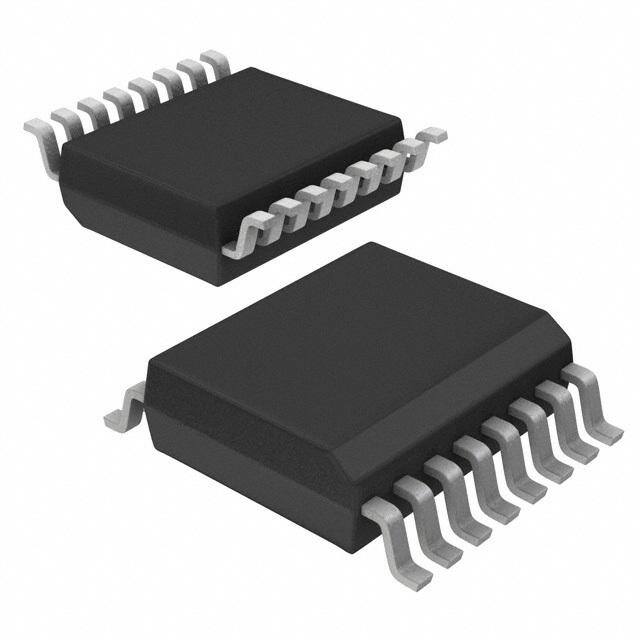
| 供应商器件封装 | 16-SSOP |
| 关闭 | No Shutdown |
| 其它名称 | 568-4512-1 |
| 准确性 | +/- 3 C to +/- 5 C |
| 功能 | 温度监控系统(传感器) |
| 包装 | 剪切带 (CT) |
| 商标 | NXP Semiconductors |
| 安装类型 | 表面贴装 |
| 安装风格 | SMD/SMT |
| 封装 | Reel |
| 封装/外壳 | 16-SSOP(0.154",3.90mm 宽) |
| 封装/箱体 | SSOP-16 |
| 工作温度 | -55°C ~ 125°C |
| 工厂包装数量 | 2500 |
| 感应温度 | -55°C ~ 125°C, 外部传感器 |
| 拓扑 | ADC,多路复用器,寄存器库 |
| 数字输出-位数 | 8 bit |
| 数字输出-总线接口 | 2-Wire, I2C, SMBus |
| 最大工作温度 | + 125 C |
| 最小工作温度 | - 40 C |
| 标准包装 | 1 |
| 温度阈值 | Programmable |
| 特色产品 | http://www.digikey.com/cn/zh/ph/NXP/I2C.html |
| 电压-电源 | 3 V ~ 5.5 V |
| 电源电压-最大 | 5.5 V |
| 电源电压-最小 | 3 V |
| 电源电流 | 70 uA |
| 精度 | ±3°C 本地(最大), ±5°C 远程(最大) |
| 系列 | NE1617A |
| 设备功能 | System Monitor Sensor |
| 输出报警 | 是 |
| 输出类型 | Digital |
| 输出风扇 | 无 |
| 配置 | Local, Remote |
| 零件号别名 | NE1617ADS-T |


- 商务部:美国ITC正式对集成电路等产品启动337调查
- 曝三星4nm工艺存在良率问题 高通将骁龙8 Gen1或转产台积电
- 太阳诱电将投资9.5亿元在常州建新厂生产MLCC 预计2023年完工
- 英特尔发布欧洲新工厂建设计划 深化IDM 2.0 战略
- 台积电先进制程称霸业界 有大客户加持明年业绩稳了
- 达到5530亿美元!SIA预计今年全球半导体销售额将创下新高
- 英特尔拟将自动驾驶子公司Mobileye上市 估值或超500亿美元
- 三星加码芯片和SET,合并消费电子和移动部门,撤换高东真等 CEO
- 三星电子宣布重大人事变动 还合并消费电子和移动部门
- 海关总署:前11个月进口集成电路产品价值2.52万亿元 增长14.8%


PDF Datasheet 数据手册内容提取
NE1617A Temperature monitor for microprocessor systems Rev. 5 — 20 March 2012 Product data sheet 1. General description The NE1617A is an accurate two-channel temperature monitor. It measures the temperature of itself and the temperature of a remote sensor. The remote sensor is a diode connected transistor. This can be in the form of either a discrete NPN/PNP, such as the 2N3904/2N3906, or a diode connected PNP built into another die, such as is done on some Intel microprocessors. The temperature of both the remote and local sensors is stored in a register that can be read via a 2-wire SMBus. The temperatures are updated at a rate that is programmable via the SMBus (the average supply current is dependent upon the update rate — the faster the rate, the higher the current). In addition to the normal operation, which is to update the temperature at the programmed rate, there is a one-shot mode that will force a temperature update. There is also an alarm that senses either an overtemperature or undertemperature condition. The trip points for this alarm are also programmable. The device can have one of nine addresses (determined by two address pins), so there can be up to nine of the NE1617A on the SMBus. It can also be put in standby mode (in order to save power). This can be done either with software (over the SMBus) or with hardware (using the STBY pin). 2. Features and benefits Replacement for Maxim MAX1617 and Analog Devices ADM1021 Monitors local and remote temperature Local (on-chip) sensor accuracy: 2C at 60C to 100C 3C at 40C to 125C Remote sensor accuracy: 3C at 60C to 100C 5C at 40C to 125C No calibration required Programmable overtemperature/undertemperature alarm SMBus 2-wire serial interface up to 100kHz 3V to 5.5V supply range; 5.5V tolerant 70A supply current in operating mode 3A (typical) supply current in standby mode
NE1617A NXP Semiconductors Temperature monitor for microprocessor systems ESD protection exceeds 2000V HBM per JESD22-A114 and 1000V CDM per JESD22-C101 Latch-up testing is done to JEDEC standard JESD78, which exceeds 100mA Small 16-lead SSOP (QSOP) package 3. Applications Desktop computers Notebook computers Smart battery packs Industrial controllers Telecommunications equipment 4. Ordering information Table 1. Ordering info rmation T = 40C to +125C. amb Type number Topside Package mark Name Description Version NE1617ADS NE1617A SSOP16[1] plastic shrink small outline package; 16leads; bodywidth3.9mm; SOT519-1 lead pitch 0.635mm [1] Also known as QSOP16. NE1617A All information provided in this document is subject to legal disclaimers. © NXP B.V. 2012. All rights reserved. Product data sheet Rev. 5 — 20 March 2012 2 of 30
NE1617A NXP Semiconductors Temperature monitor for microprocessor systems 5. Block diagram STBY NE1617A ONE-SHOT CONFIGURATION COMMAND POINTER LOCAL REGISTER REGISTER REGISTER CONTROL TEMP LOGIC SENSOR CONVERSION RATE LOCAL HIGH TEMP LOCAL TEMP HIGH REGISTER THRESHOLD LIMIT REGISTER LOCAL TEMP LOCAL LOW TEMP LOCAL TEMP LOW D+ ANALOG A-to-D DATA REGISTER THRESHOLD LIMIT REGISTER D− MUX CONVERTER REMOTE TEMP REMOTE HIGH TEMP REMOTE TEMP HIGH DATA REGISTER THRESHOLD LIMIT REGISTER ADD1 ADDRESS REMOTE LOW TEMP REMOTE TEMP LOW ADD0 DECODER THRESHOLD LIMIT REGISTER ALERT INTERRUPT STATUS REGISTER MASKING SMBus INTERFACE VDD GND GND TEST1 TEST5 TEST9 TEST13 TEST16 SCLK SDATA 002aad510 Fig 1. Block diagram of NE1617A NE1617A All information provided in this document is subject to legal disclaimers. © NXP B.V. 2012. All rights reserved. Product data sheet Rev. 5 — 20 March 2012 3 of 30
NE1617A NXP Semiconductors Temperature monitor for microprocessor systems 6. Pinning information 6.1 Pinning TEST1 1 16 TEST16 VDD 2 15 STBY D+ 3 14 SCLK D− 4 13 TEST13 NE1617ADS TEST5 5 12 SDATA ADD1 6 11 ALERT GND 7 10 ADD0 GND 8 9 TEST9 002aad509 Fig 2. Pin configuration for SSOP16 (QSOP16) 6.2 Pin description Table 2. Pin description Symbol Pin Description TEST1 1 test pin; factory use only[1] V 2 positive supply[2] DD D+ 3 positive side of remote sensor D 4 negative side of remote sensor TEST5 5 test pin; factory use only[1] ADD1 6 device address 1 (3-state) GND 7, 8 ground TEST9 9 test pin; factory use only[1] ADD0 10 device address 0 (3-state) ALERT 11 open-drain output used as interrupt or SMBus alert SDATA 12 SMBus serial data input/output; open-drain TEST13 13 test pin; factory use only[1] SCLK 14 SMBus clock input STBY 15 hardware standby input HIGH=normal operating mode LOW=standby mode TEST16 16 test pin; factory use only[1] [1] These pins should either float or be tied to ground. [2] VDD pin should be decoupled by a 0.1F capacitor. NE1617A All information provided in this document is subject to legal disclaimers. © NXP B.V. 2012. All rights reserved. Product data sheet Rev. 5 — 20 March 2012 4 of 30
NE1617A NXP Semiconductors Temperature monitor for microprocessor systems 7. Functional description The NE1617A contains an integrating A-to-D converter, an analog multiplexer, a status register, digital data registers, SMBus interface, associated control logic and a local temperature sensor or channel (refer to Figure 1 “Block diagram of NE1617A”). The remote diode-type sensor or channel should be connected to the D+ and D pins properly. Temperature measurements or conversions are either automatically and periodically activated when the device is in free-running mode (both STBY pin = HIGH, and the configuration register bit6=LOW) or generated by one-shot command. The free-running period is selected by changing the programmable data of the conversion rate register, as described in Section8.3.4. For each conversion, the multiplexer switches current sources through the remote and local temperature sensors over a period of time, about 60ms, and the voltages across the diode-type sensors are sensed and converted into the temperature data by the A-to-D converter. The resulting temperature data is then stored in the temperature registers, in 8-bit two's complement word format and automatically compared with the limits which have been programmed in the temperature limit registers. Results of the comparison are reflected accordingly by the flags stored in the status register, an out-of-limit condition will set the ALERT output pin to its LOW state. Because both channels are automatically measured for each conversion, the results are updated for both channels at the end of every successful conversion. 7.1 Temperature measurement The method of the temperature measurement is based on the change of the diode V at BE two different operating current levels given by: V = nK-----T-- LNN (1) BE q where: V =change in base emitter voltage drop at two current levels BE n = non-ideality K = Boltzman’s constant T = absolute temperature in Kelvin q = charge on the electron LN = natural logarithm N = ratio of the two currents The NE1617A forces two well-controlled current sources of about 10A and 100A and measures the remote diode V . The sensed voltage between two pins D+ and D is BE limited between 0.25V and 0.95V. The external diode must be selected to meet this voltage range at these two current levels and also the non-ideality factor ‘n’ must be close to the value of 1.008 to be compatible with the Intel Pentium III internal thermal diode that the NE1617A was designed to work with. The diode-connected PNP transistor provided on the microprocessor is typically used, or the discrete diode-connected transistor 2N3904 or 2N3906 is recommended as an alternative. NE1617A All information provided in this document is subject to legal disclaimers. © NXP B.V. 2012. All rights reserved. Product data sheet Rev. 5 — 20 March 2012 5 of 30
NE1617A NXP Semiconductors Temperature monitor for microprocessor systems Even though the NE1617A integrating A-to-D converter has a good noise performance, using the average of 10 measurement cycles, high frequency noise filtering between D+ and D should be considered. An external capacitor of 2200pF typical (but not higher than 3300pF) connected between D+ and D is recommended. Capacitance higher than 3300pF will introduce measurement error due to the rise time of the switched current source. 7.2 No calibration is required As mentioned in Section7.1, the NE1617A uses two well-controlled current sources of 10:1 ratio to measure the forward voltage of the diode (V ). This technique eliminates BE the diode saturation current (a heavily process and temperature dependent variable), and results in the forward voltage being proportional to absolute temperature. 7.3 Address logic The address pins of the NE1617A can be forced into one of three levels: LOW (GND), HIGH (V ), or ‘not connected’ (n.c.). Because the NE1617A samples and latches the DD address pins at the starting of every conversion, it is suggested that those address pins should be hard-wired to the logic applied, so that the logic is consistently existed at the address pins. During the address sensing period, the device forces a current at each address pin and compares the voltage developed across the external connection with the predefined threshold voltage in order to define the logic level. If an external resistor is used for the connection of the address, then its value should be less than 2k to prevent the error in logic detection from happening. Resistors of 1k are recommended. 8. Temperature monitor with SMBus serial interface 8.1 Serial bus interface The device can be connected to a standard 2-wire serial interface System Management Bus (SMBus) as a slave device under the control of a master device, using two device terminals SCLK and SDATA. The operation of the device to the bus is described with details in the following sections. 8.2 Slave address The device address is defined by the logical connections applied to the device pins ADD0 and ADD1. A list of selectable addresses are shown in Table3. The device address can be set to any one of those nine combinations and more than one device can reside on the same bus without address conflict. Note that the state of the device address pins is sampled and latched not only at power-up step, but also at starting point of every conversion. Table 3. Device slave address n.c. = not connected ADD0[1] ADD1[1] Address byte GND GND 0011000 GND n.c. 0011001 GND V 0011010 DD n.c. GND 0101001 NE1617A All information provided in this document is subject to legal disclaimers. © NXP B.V. 2012. All rights reserved. Product data sheet Rev. 5 — 20 March 2012 6 of 30
NE1617A NXP Semiconductors Temperature monitor for microprocessor systems Table 3. Device slave address …continued n.c. = not connected ADD0[1] ADD1[1] Address byte n.c. n.c. 0101010 n.c. V 0101011 DD V GND 1001100 DD V n.c. 1001101 DD V V 1001110 DD DD [1] Any pull-up/pull-down resistor used to connect to GND or VDD should be 2k. 8.3 Registers The device contains more than 9 registers. They are used to store the data of device set-up and operation results. Depending on the bus communication (either read or write operations), each register may be called by different names because each register may have different sub-addresses or commands for read and write operations. For example, the configuration register is called as WC for write mode and as RC for read mode. Table4 shows the names, commands and functions of all registers as well as the register POR states. Remark: Attempting to write to a read-command or read from a write-command will produce an invalid result. The reserved registers are used for factory test purposes and should not be written. Table 4. Register assignments Register name Command byte POR state Function RIT 00h 00000000 read internal or local temp byte RET 01h 00000000 read external or remote temp byte RS 02h n/a read status byte RC 03h 00000000 read configuration byte RCR 04h 00000010 read conversion rate byte RIHL 05h 01111111 read internal temp high limit byte RILL 06h 11001001 read internal temp low limit byte REHL 07h 01111111 read external temp high limit byte RELL 08h 11001001 read external temp low limit byte WC 09h n/a write configuration byte WCR 0Ah n/a write conversion rate byte WIHL 0Bh n/a write internal temp high limit byte WILL 0Ch n/a write internal temp low limit byte WEHL 0Dh n/a write external temp high limit byte WELL 0Eh n/a write external temp low limit byte OSHT 0Fh n/a one-shot command - 10h n/a reserved - 11h n/a reserved - 12h n/a reserved - 13h n/a reserved NE1617A All information provided in this document is subject to legal disclaimers. © NXP B.V. 2012. All rights reserved. Product data sheet Rev. 5 — 20 March 2012 7 of 30
NE1617A NXP Semiconductors Temperature monitor for microprocessor systems 8.3.1 Low power standby modes Upon POR, the device is reset to its normal free-running auto-conversion operation mode. The device can be put into standby mode by either using hardware control (connect the STBY pin to LOW for hardware standby mode) or using software control (set bit6 of the configuration register to HIGH for software standby mode). When the device is put in either one of the standby modes, the supply current is reduced to less than 10 A if there is no SMBus activity, all data in the device registers are retained and the SMBus interface is still alive to bus communication. However, there is a difference in the device ADC conversion operation between hardware standby and software standby modes. In hardware standby mode, the device conversion is inhibited and the one-shot command does not initiate a conversion. In software standby mode, the one-shot command will initiate a conversion for both internal and external channels. If a hardware standby command is received when the device is in normal mode and a conversion is in progress, the conversion cycle will stop and data in reading temperature registers will not be updated. 8.3.2 Configuration register The configuration register is used to mask the Alert interrupt and/or to put the device in software standby mode. Only two bits of this register (bit6 and bit7) are used as listed in Table5. Bit7 is used to mask the device ALERT output from Alert interruption when this bit is set to logic1, and bit6 is used to activate the standby software mode when this bit is set to logic1. This register can be written or read using the commands of registers named WC and RC accordingly. Upon Power-On Reset (POR), both bits are reset to zero. Table 5. Configuration register bit assignments Bit Symbol POR state Function 7 (MSB) MASK 0 Mask ALERT interrupt. Interrupt is enabled when this bit is LOW, and disabled when this bit is HIGH. 6 RUN/STOP 0 Standby or run mode control. When LOW, running mode is enabled; when HIGH, standby mode is initiated. 5 to 0 - n/a reserved 8.3.3 External and internal temperature registers Results of temperature measurements after every ADC conversion are stored in two registers: Internal Temp register (RIT) for internal or local diode temperature, and External Temp register (RET) for external or remote diode temperature. These registers can be only read over the SMBus. The reading temperature data is in 2'scomplement binary form consisting of 7-bit data and 1-bit sign (MSB), with each data count represents 1C, and the MSB bit is transmitted first over the serial bus. The contents of those two registers are updated upon completion of each ADC conversion. Table6 shows some values of the temperature and data. NE1617A All information provided in this document is subject to legal disclaimers. © NXP B.V. 2012. All rights reserved. Product data sheet Rev. 5 — 20 March 2012 8 of 30
NE1617A NXP Semiconductors Temperature monitor for microprocessor systems Table 6. Temperature data format (2’s complement) Temperature (C) Digital output (8bits) +127 01111111 +126 01111110 +100 01100100 +50 00110010 +25 00011001 +1 00000001 0 00000000 1 11111111 25 11100111 50 11001110 65 10111111 8.3.4 Conversion rate register The conversion rate register is used to store programmable conversion data, which defines the time interval between conversions in standard free-running auto-convert mode. Table7 shows all applicable data and rates for the device. Only three LSB bits of the register are used and other bits are reserved for future use. This register can be written to and read back over the SMBus using commands of the registers named WCR and RCR, respectively. The POR default conversion data is 02h (0.25Hz). Notice that the average supply current, as well as the device power consumption, is increased with the conversion rate. Table 7. Conversion rate control byte Data Conversion rate (Hz) Average supply current (A typical at V =3.3V) DD 00h 0.0625 67 01h 0.125 68 02h 0.25 70 03h 0.5 75 04h 1 80 05h 2 95 06h 4 125 07h 8 180 08h to FFh (reserved) n/a 8.3.5 Temperature limit registers The device has four registers to be used for storing programmable temperature limits, including the high limit and the low limit for each channel of the external and internal diodes. Data of the temperature register (RIT and RET) for each channel are compared with the contents of the temperature limit registers of the same channel, resulting in alarm conditions. If measured temperature either equals or exceeds the corresponding temperature limits, an Alert interrupt is asserted and the corresponding flag bit in the status register is set. The temperature limit registers can be written to and read back using NE1617A All information provided in this document is subject to legal disclaimers. © NXP B.V. 2012. All rights reserved. Product data sheet Rev. 5 — 20 March 2012 9 of 30
NE1617A NXP Semiconductors Temperature monitor for microprocessor systems commands of registers named WIHL, WILL, WEHL, WELL, RIHL, RILL, REHL, RELL, accordingly. The POR default values are +127C (01111111) for the HIGH limit and 55C (11001001) for the LOW limit. 8.3.6 One-shot command The one-shot command is not actually a data register as such and a write operation to it will initiate an ADC conversion. The send byte format of the SMBus, as described later, with the use of OSHT command (0Fh), is used for this writing operation. In normal free-running-conversion operation mode of the device, a one-shot command immediately forces a new conversion cycle to begin. However, if a conversion is in progress when a one-shot command is received, the command is ignored. In software standby mode the one-shot command generates a single conversion and comparison cycle and then puts the device back in its standby mode after the conversion. In hardware standby mode, the one shot is inhibited. 8.3.7 Status register The content of the status register reflects condition status resulting from all of these activities: comparisons between temperature measurements and temperature limits, the status of ADC conversion, and the hardware condition of the connection of external diode to the device. Bit assignments and bit functions of this register are listed in Table8. This register can only be read using the command of register named RS. Upon POR, the status of all flag bits are reset to zero. The status byte is cleared by any successful read of the status register unless the fault condition persists. Notice that any one of the fault conditions, except the conversion busy, also introduces an Alert interrupt to the SMBus that will be described in Section8.3.8. Also, whenever a one-shot command is executed, the status byte should be read after the conversion is completed, which is about 170ms after the one-shot command is sent. Table 8. Status register bit assignment Bit Symbol POR state Function 7 (MSB) BUSY n/a HIGH when the ADC is busy converting 6 IHLF[1] 0 HIGH when the internal temperature high limit has tripped 5 ILLF[1] 0 HIGH when the internal temperature low limit has tripped 4 EHLF[1] 0 HIGH when the external temperature high limit has tripped 3 ELLF[1] 0 HIGH when the external temperature low limit has tripped 2 OPEN[2] 0 HIGH when the external diode is opened 1 to 0 - 0 reserved [1] These flags stay HIGH until the status register is read or POR is activated. [2] This flag stays HIGH until POR is activated. 8.3.8 Alert interrupt The ALERT output is used to signal Alert interruption from the device to the SMBus and is activeLOW. Because this output is an open-drain output, a pull-up resistor (10k typical) to V is required, and slave devices can share a common interrupt line on the same DD SMBus. An Alert interrupt is asserted by the device whenever any one of the fault conditions, as described in Section 8.3.7 “Status register”, occurs: measured temperature equals or exceeds corresponding temp limits, the remote diode is physically disconnected from the device pins. Alert interrupt signal is latched and can only be cleared by reading NE1617A All information provided in this document is subject to legal disclaimers. © NXP B.V. 2012. All rights reserved. Product data sheet Rev. 5 — 20 March 2012 10 of 30
NE1617A NXP Semiconductors Temperature monitor for microprocessor systems the Alert Response byte from the Alert Response Address, which is a special slave address to the SMBus. The ALERT output cannot be reset by reading the device status register. The device was designed to accommodate the Alert interrupt detection capability of the SMBus.1 Basically, the SMBus provides Alert response interrupt pointers in order to identify the slave device which has caused the Alert interrupt. The 7-bit Alert response slave address is 0001100 and the Alert response byte reflects the slave address of the device which has caused Alert interrupt. Bit assignments of the Alert response byte are listed in Table9. The ALERT output will be reset to HIGH state upon reading the Alert response slave address unless the fault condition persists. Table 9. Alert response (Alert response address 0001100) bit description Bit Symbol Description 7 (MSB) ADD7 indicate address B6 of alerted device 6 ADD6 indicate address B5 of alerted device 5 ADD5 indicate address B4 of alerted device 4 ADD4 indicate address B3 of alerted device 3 ADD3 indicate address B2 of alerted device 2 ADD2 indicate address B1 of alerted device 1 ADD1 indicate address B0 of alerted device 0 (LSB) 1 logic1 8.4 Power-up default condition Upon power-up reset (power is switched off-on), the NE1617A goes into this default condition: • Interrupt latch is cleared, the ALERT output is pulled HIGH by the external pull-up resistor. • The auto-conversion rate is at 0.25Hz; conversion rate data is 02h. • Temperature limits for both channels are +127C for high limit, and 55C for low limit. • Command pointer register is set to ‘00’ for quickly reading the RIT. 8.5 Fault detection The NE1617A has a fault detector to the diode connection. The connection is checked when a conversion is initiated and the proper flags are set if the fault condition has occurred. Table 10. Fault detection D+ and D ALERT output RET data storage Status set flag opened LOW 127C B2 and B4 shorted LOW 127C B4 1. The NE1617A implements the collision arbitration function per System Management Bus Specification Revision 1.1, dated December 11, 1998, which conforms to standard I2C-bus arbitration as described in NXP document UM10204, “I2C-bus specification and user manual”. NE1617A All information provided in this document is subject to legal disclaimers. © NXP B.V. 2012. All rights reserved. Product data sheet Rev. 5 — 20 March 2012 11 of 30
NE1617A NXP Semiconductors Temperature monitor for microprocessor systems 8.6 SMBus interface The device can communicate over a standard 2-wire serial interface System Management Bus (SMBus) using the device pins SCLK and SDATA. The device employs four standard SMBus protocols: writebyte, readbyte, sendbyte and receivebyte. Data formats of those protocols are shown in Figure3 with following notifications: • The SMBus master initiates data transfer by establishing a START condition (S) and terminates data transfer by generating a STOP condition (P). • Data is sent over the serial bus in sequence of 9 clock pulses according to each 8-bit data byte followed by 1-bit status of the device acknowledgement. • The 7-bit slave address is equivalent to the selected address of the device. • The command byte is equivalent to the selected command of the device register. • The ‘send byte’ format is often used for the one-shot conversion command. • The ‘receive byte’ format is used for quicker transfer data from a device reading register that was previously selected by a readbyte format. address ACK command ACK data ACK S 7 bits device address 0 8 bits device register 8 bits to register P START condition R/W acknowledged acknowledged acknowledged STOP by device by device by device condition 002aad523 a. Writebyte format (for writing data byte to the device register) address ACK command ACK address ACK data NACK S 7 bits device address 0 8 bits device register S 7 bits device address 1 8 bits from register P START condition R/W acknowledged acknowledged (re)START R/W acknowledged not STOP by device by device condition by device acknowledged condition by controller 002aad524 b. Readbyte format (for reading data byte from the device register) address ACK command ACK S 7 bits device address 0 8 bits device register P START condition R/W acknowledged acknowledged STOP by device by device condition 002aad525 c. Sendbyte format (for sending command without data, such as one-shot command) address ACK data NACK S 7 bits device address 1 8 bits from register P START condition R/W acknowledged not STOP by device acknowledged condition by controller 002aad526 d. Receivebyte format (for continuously reading from device register) Fig 3. SMBus programming format NE1617A All information provided in this document is subject to legal disclaimers. © NXP B.V. 2012. All rights reserved. Product data sheet Rev. 5 — 20 March 2012 12 of 30
NE1617A NXP Semiconductors Temperature monitor for microprocessor systems 9. Application design-in information 9.1 Factors affecting accuracy 9.1.1 Remote sensing diode The NE1617A is designed to work with substrate transistors built into processors’ CPUs or with discrete transistors. Substrate transistors are generally PNP types with the collector connected to the substrate. Discrete types can be either a PNP or an NPN transistor connected as a diode (base shorted to collector). If an NPN transistor is used, the collector and base are connected to D+ and the emitter to D. If a PNP transistor is used, the collector and base are connected to D and the emitter to D+. Substrate transistors are found in a number of CPUs. To reduce the error due to variations in these substrate and discrete transistors, a number of factors should be taken into consideration: • The ideality factor, n, of the transistor. The ideality factor is a measure of the deviation f of the thermal diode from the ideal behavior. The NE1617A is trimmed for an n value f of 1.008. Equation2 can be used to calculate the error introduced at a temperature TC when using a transistor whose n does not equal 1.008. Consult the processor f data sheet for n values. f This value can be written to the offset register and is automatically added to or subtracted from the temperature measurement. n –1.008 T = ------n---a--t--u---r--a--l----------------------273.15 Kelvin+T (2) 1.008 • Some CPU manufacturers specify the high and low current levels of the substrate transistors. The I high current level of the NE1617A is 100A and the low level source current is 10A. If a discrete transistor is being used with the NE1617A, the best accuracy is obtained by choosing devices according to the following criteria: • Base-emitter voltage greater than 0.25V at 6mA, at the highest operating temperature. • Base-emitter voltage less than 0.95V at 100mA, at the lowest operating temperature. • Base resistance less than 100. • Small variation in h (say 50 to 150) that indicates tight control of V characteristics. FE BE Transistors such as 2N3904, 2N3906, or equivalents in SOT23 packages are suitable devices to use. See Table11 for representative devices. NE1617A All information provided in this document is subject to legal disclaimers. © NXP B.V. 2012. All rights reserved. Product data sheet Rev. 5 — 20 March 2012 13 of 30
NE1617A NXP Semiconductors Temperature monitor for microprocessor systems Table 11. Representative diodes for temperature sensing Manufacturer Model number Rohm UMT3904 Diodes Inc. MMBT3904-7 Philips MMBT3904 ST Micro MMBT3904 ON Semiconductor MMBT3904LT1 Chenmko MMBT3904 Infineon Technologies SMBT3904E6327 Fairchild Semiconductor MMBT3904FSCT National Semiconductor MMBT3904N623 9.1.2 Thermal inertia and self-heating Accuracy depends on the temperature of the remote-sensing diode and/or the internal temperature sensor being at the same temperature as that being measured, and a number of factors can affect this. Ideally, the sensor should be in good thermal contact with the part of the system being measured, for example, the processor. If it is not, the thermal inertia caused by the mass of the sensor causes a lag in the response of the sensor to a temperature change. In the case of the remote sensor, this should not be a problem, since it is either a substrate transistor in the processor or a small package device, such as the SOT23, placed in close proximity to it. The on-chip sensor, however, is often remote from the processor and is only monitoring the general ambient temperature around the package. The thermal time constant of the SSOP16 package in still air is about 140seconds, and if the ambient air temperature quickly changed by 100C, it would take about 12minutes (five time constants) for the junction temperature of the NE1617A to settle within 1C of this. In practice, the NE1617A package is in electrical and therefore thermal contact with a printed-circuit board and can also be in a forced airflow. How accurately the temperature of the board and/or the forced airflow reflect the temperature to be measured also affects the accuracy. Self-heating due to the power dissipated in the NE1617A or the remote sensor causes the chip temperature of the device or remote sensor to rise above ambient. However, the current forced through the remote sensor is so small that self-heating is negligible. In the case of the NE1617A, the worst-case condition occurs when the device is converting at 16conversions per second while sinking the maximum current of 1mA at the ALERT output. In this case, the total power dissipation in the device is about 11mW. The thermal resistance, R , of the SSOP16 package is about 121C/W. th(j-a) In practice, the package has electrical and therefore thermal connection to the printed circuit board, so the temperature rise due to self-heating is negligible. NE1617A All information provided in this document is subject to legal disclaimers. © NXP B.V. 2012. All rights reserved. Product data sheet Rev. 5 — 20 March 2012 14 of 30
NE1617A NXP Semiconductors Temperature monitor for microprocessor systems 9.1.3 Layout considerations Digital boards can be electrically noisy environments, and the NE1617A is measuring very small voltages from the remote sensor, so care must be taken to minimize noise induced at the sensor inputs. The following precautions should be taken. 1. Place the NE1617A as close as possible to the remote sensing diode. Provided that the worst noise sources, that is, clock generators, data/address buses, and CRTs, are avoided, this distance can be four to eight inches. 2. Route the D+ and D tracks close together, in parallel, with grounded guard tracks on each side. Provide a ground plane under the tracks if possible. 3. Use wide tracks to minimize inductance and reduce noise pickup. 10mil track minimum width and spacing is recommended (see Figure4). 4. Try to minimize the number of copper/solder joints, which can cause thermocouple effects. Where copper/solder joints are used, make sure that they are in both the D+ and D path and at the same temperature. Thermocouple effects should not be a major problem since 1C corresponds to about 200V and thermocouple voltages are about 3V/C of temperature difference. Unless there are two thermocouples with a big temperature differential between them, thermocouple voltages should be much less than 200V. 5. Place a 0.1F bypass capacitor close to the V pin. In very noisy environments, DD place a 1000pF input filter capacitor across D+ and D close to the NE1617A. 6. If the distance to the remote sensor is more than eight inches, the use of twisted pair cable is recommended. This works up to about sixfeet to 12feet. 7. For really long distances (up to 100feet), use shielded twisted pair, such as Belden#8451 microphone cable. Connect the twisted pair to D+ and D and the shield to GND close to the NE1617A. Leave the remote end of the shield unconnected to avoid ground loops. Because the measurement technique uses switched current sources, excessive cable and/or filter capacitance can affect the measurement. When using long cables, the filter capacitor can be reduced or removed. Cable resistance can also introduce errors. 1 resistance introduces about 1C error. GND 10 mil 10 mil D+ 10 mil 10 mil D− 10 mil 10 mil GND 10 mil 002aag953 Fig 4. Typical arrangement of signal tracks NE1617A All information provided in this document is subject to legal disclaimers. © NXP B.V. 2012. All rights reserved. Product data sheet Rev. 5 — 20 March 2012 15 of 30
NE1617A NXP Semiconductors Temperature monitor for microprocessor systems 9.2 Power sequencing considerations 9.2.1 Power supply slew rate When powering-up the NE1617A, ensure that the slew rate of V is less than 18mV/s. DD A slew rate larger than this may cause power-on reset issues and yield unpredictable results. 9.2.2 Application circuit Figure5 shows a typical application circuit for the NE1617A, using a discrete sensor transistor connected via a shielded, twisted pair cable. The pull-ups on SCLK, SDATA, and ALERT are required only if they are not already provided elsewhere in the system. The SCLK and SDATA pins of the NE1617A can be interfaced directly to the SMBus of an I/O controller, such as the Intel 820 chipset. 0.1 μF VDD 2 15 R R R VDD STBY 10 kΩ 10 kΩ 10 kΩ NE1617A 3 14 D+ SCLK clock C1(1) 12 2200 pF SDATA data 4 D− 11 remote sensor ALERT microcontroller 2N3904 (NPN), interrupt 2N3906 (PNP) or similar stand-alone ASIC or processor thermal diode ADD0 ADD1 GND GND 10 6 7 8 002aad511 (1) Typical value, placed close to temperature sensor. Fig 5. Typical application circuit NE1617A All information provided in this document is subject to legal disclaimers. © NXP B.V. 2012. All rights reserved. Product data sheet Rev. 5 — 20 March 2012 16 of 30
NE1617A NXP Semiconductors Temperature monitor for microprocessor systems 10. Limiting values Table 12. Limiting values In accordance with the Absolute Maximum Rating System (IEC 60134). Symbol Parameter Conditions Min Max Unit V supply voltage V to GND 0.3 +6 V DD DD V input voltage D+, ADD0, ADD1 0.3 V +0.3 V I DD D to GND 0.3 +0.8 V SCLK, SDATA, ALERT, STBY 0.3 +6 V I input current SDATA 1 +50 mA I D - 1 mA T ambient temperature operating 55 +125 C amb T maximum junction - +150 C j(max) temperature T storage temperature 65 +150 C stg NE1617A All information provided in this document is subject to legal disclaimers. © NXP B.V. 2012. All rights reserved. Product data sheet Rev. 5 — 20 March 2012 17 of 30
NE1617A NXP Semiconductors Temperature monitor for microprocessor systems 11. Characteristics Table 13. Characterist ics V =3.0V to 3.6V; T =0C to +125C; unless otherwise specified. DD amb Symbol Parameter Conditions Min Typ Max Unit T temperature resolution 1 - - C res T local temperature accuracy T =+60C to +100C - <1 2 C acc(loc) amb T =0C to +125C - <2 3 C amb T remote temperature accuracy T =+60C to +100C - - 3 C acc(rem) remote T =40C to +125C - - 5 C remote V undervoltage lockout threshold V supply[2] - 2.7 2.95 V th(UVLO) DD voltage[1] V power-on reset threshold V supply (falling edge)[3] 1.0 - 2.5 V th(POR) DD voltage I average supply current conversion rate = 0.25 per second - - 70 A DD(AV) conversion rate = 2 per second - - 180 A I standby supply current SMBus inactive - 3 10 A DD(stb) t conversion time from STOP bit to conversion - - 170 ms conv complete; both channels E conversion rate error percentage error in programmed 30 - +30 % f(conv) rate I source current remote sensor source HIGH level - 100 - A LOW level - 10 - A I bias current ADD0, ADD1; momentary as the [4][5] - 160 - A bias address is being read [1] The value of V below which the internal A/D converter is disabled. This is designed to be a minimum of 200mV above the power-on DD reset. During the time that it is disabled, the temperature that is in the ‘read temperature registers’ will remain at the value that it was before the ADC was disabled. This is done to eliminate the possibility of reading unexpected false temperatures due to the A/D converter not working correctly due to low voltage. In case of power-up (rising VDD), the reading that is stored in the ‘read temperature registers’ will be the default value of 0C. As soon as VDD has risen to the value of UVLO, the ADC will function correctly and normal temperatures will be read. [2] V (rising edge) voltage below which the ADC is disabled. DD [3] V (falling edge) voltage below which the logic is reset. DD [4] Address is read at power-up and at start of conversion for all conversions except the fastest rate. [5] Due to the bias current, any pull-up/pull-down resistors should be 2k. NE1617A All information provided in this document is subject to legal disclaimers. © NXP B.V. 2012. All rights reserved. Product data sheet Rev. 5 — 20 March 2012 18 of 30
NE1617A NXP Semiconductors Temperature monitor for microprocessor systems Table 14. Characterist ics V =3.3V; T =40C to +125C; unless otherwise specified.[1] DD amb Symbol Parameter Conditions Min Typ Max Unit ADC and power supply T temperature resolution monotonicity guaranteed [2] 8 - - bits res T local temperature accuracy[3] T =+60C to +100C - <1 2 C acc(loc) amb T =40C to +125C - <2 3 C amb T remote temperature T =+60C to +100C [4] - - 3 C acc(rem) remote accuracy[3] T =40C to +125C [4] - - 5 C remote V supply voltage 3.0 - 5.5 V DD t conversion time from STOP bit to conversion - 125 156 ms conv complete; both channels E conversion rate error percentage error in programmed 25 - +25 % f(conv) rate SMBus interface V HIGH-level input voltage STBY, SCLK, SDATA IH V =3V 2.2 - - V DD V =5.5V 2.4 - - V DD V LOW-level input voltage STBY, SCLK, SDATA; - - 0.8 V IL V =3Vto5.5V DD I sink current logic output LOW; 6 - - mA sink ALERT,SDATAforced to 0.4V I HIGH-level output leakage ALERT; forced to 5.5V - - 1 A LOH current I input current logic inputs forced to V or GND 2 - +2 A I DD [1] Specifications from 40C to +125C are guaranteed by design, not production tested. [2] Guaranteed but not 100% tested. [3] Quantization error is not included in specifications for temperature accuracy. For example, if the NE1617A device temperature is exactly +66.7C, the ADC may report +66C, +67C or +68C (due to the quantization error plus the 0.5C offset used for rounding up) and still be within the guaranteed 1C error limits for the +60C to +100C temperature range. [4] Tremote is the junction temperature of the remote diode. See Section 7.1 “Temperature measurement” for remote diode forward voltage requirements. NE1617A All information provided in this document is subject to legal disclaimers. © NXP B.V. 2012. All rights reserved. Product data sheet Rev. 5 — 20 March 2012 19 of 30
NE1617A NXP Semiconductors Temperature monitor for microprocessor systems Table 15. SMBus inter face dynamic characteristics[1] V =3.0V to 3.6V; T =0C to +125C; unless otherwise specified.[2] DD amb Symbol Parameter Conditions Min Typ Max Unit V HIGH-level input voltage STBY, SCLK, SDATA 2.2 - - V IH V LOW-level input voltage STBY, SCLK, SDATA - - 0.8 V IL I logic output LOW sink current ALERT; V =0.4V 1.0 - - mA OL OL SDATA; V =0.6V 6.0 - - mA OL I HIGH-level input current V =V 1 - +1 A IH I DD I LOW-level input current V =GND 1 - +1 A IL I C input capacitance SCLK, SDATA - 5 - pF i f SCLK operating frequency 0 - 100 kHz SCLK t SCLK LOW time 4.7 5.0 - s LOW t SCLK HIGH time 4.0 5.0 - s HIGH t bus free time between a STOP from SDATA STOP 4.7 - - s BUF and START condition toSDATASTART t hold time (repeated) START from SDATA START to first SCLK 4.0 - - s HD;STA condition HIGH-to-LOW transition t data hold time from SCLK HIGH-to-LOW transition 0 - - ns HD;DAT to SDATA edges t data set-up time from SDATA edges 250 - - ns SU;DAT toSCLKLOW-to-HIGH transition t set-up time for a repeated from SCLK LOW-to-HIGH transition 250 - - ns SU;STA START condition to restart SDATA t set-up time for STOP condition from SCLK LOW-to-HIGH transition 4.0 - - s SU;STO to SDATA STOP condition t fall time SCLK and SDATA signals - - 1.0 s f [1] The NE1617A does not include the SMBus time-out capability (t and t ). LOW;SEXT LOW;MEXT [2] Device operation between 3.0V and 5.5V is allowed, but parameters may be outside the limit shown in this table. tLOW tr tf tHD;STA SCLK tHD;STA tHIGH tSU;STA tSU;STO tHD;DAT tSU;DAT SDATA tBUF P S S P 002aae777 Fig 6. Timing measurements NE1617A All information provided in this document is subject to legal disclaimers. © NXP B.V. 2012. All rights reserved. Product data sheet Rev. 5 — 20 March 2012 20 of 30
NE1617A NXP Semiconductors Temperature monitor for microprocessor systems 11.1 Typical performance curves 002aab749 002aab747 20 6 temp. error temp. (°C) error (°C) 10 D+ to GND 2 0 −2 −10 D+ to VDD −20 −6 1 10 102 1 10 102 103 104 leakage resistance (MΩ) f (kHz) VI=100mVpp and AC-coupled to D Fig 7. Temperature error versus printed-circuit board Fig 8. Temperature error versus common-mode leakage resistance noise frequency 002aab748 002aab750 6 10 temp. temp. error error (°C) (°C) 2 0 −2 −10 −6 −20 1 10 102 103 104 0 40 80 120 f (kHz) D+ to D− capacitance (nF) VI=100mVpp and AC-coupled to D and D+ Fig 9. Temperature error versus differential mode Fig 10. Temperature error versus D+ to D noise frequency capacitance NE1617A All information provided in this document is subject to legal disclaimers. © NXP B.V. 2012. All rights reserved. Product data sheet Rev. 5 — 20 March 2012 21 of 30
NE1617A NXP Semiconductors Temperature monitor for microprocessor systems 002aad517 002aad518 100 130 ID(Dμ(Ast)b) (IμDAD) 80 110 60 90 40 70 20 0 50 1 10 102 103 10−2 10−1 1 10 fSCLK (kHz) conversion rate (kHz) Fig 11. Standby supply current versus clock Fig 12. Operating supply current versus conversion frequency at V =3.3V rate at V =3.3V DD DD 002aad519 150 temperature (°C) 100 50 0 0 2 6 10 time (s) Fig 13. Response to thermal shock immersed in +115C fluorinert bath NE1617A All information provided in this document is subject to legal disclaimers. © NXP B.V. 2012. All rights reserved. Product data sheet Rev. 5 — 20 March 2012 22 of 30
NE1617A NXP Semiconductors Temperature monitor for microprocessor systems 12. Package outline SSOP16: plastic shrink small outline package; 16 leads; body width 3.9 mm; lead pitch 0.635 mm SOT519-1 D E A X c y HE v M A Z 16 9 A2 A A1 (A 3 ) θ Lp L 1 8 detail X e w M bp 0 2.5 5 mm scale DIMENSIONS (mm are the original dimensions) UNIT mAax. A1 A2 A3 bp c D(1) E(1) e HE L Lp v w y Z(1) θ mm 1.73 00..2150 11..5450 0.25 00..3210 00..2158 54..08 43..08 0.635 65..28 1 00..8491 0.2 0.18 0.09 00..1085 80oo Note 1. Plastic or metal protrusions of 0.2 mm maximum per side are not included. OUTLINE REFERENCES EUROPEAN ISSUE DATE VERSION IEC JEDEC JEITA PROJECTION 99-05-04 SOT519-1 03-02-18 Fig 14. Package outline SOT519-1 (SSOP16) NE1617A All information provided in this document is subject to legal disclaimers. © NXP B.V. 2012. All rights reserved. Product data sheet Rev. 5 — 20 March 2012 23 of 30
NE1617A NXP Semiconductors Temperature monitor for microprocessor systems 13. Soldering of SMD packages This text provides a very brief insight into a complex technology. A more in-depth account of soldering ICs can be found in Application Note AN10365 “Surface mount reflow soldering description”. 13.1 Introduction to soldering Soldering is one of the most common methods through which packages are attached to Printed Circuit Boards (PCBs), to form electrical circuits. The soldered joint provides both the mechanical and the electrical connection. There is no single soldering method that is ideal for all IC packages. Wave soldering is often preferred when through-hole and Surface Mount Devices (SMDs) are mixed on one printed wiring board; however, it is not suitable for fine pitch SMDs. Reflow soldering is ideal for the small pitches and high densities that come with increased miniaturization. 13.2 Wave and reflow soldering Wave soldering is a joining technology in which the joints are made by solder coming from a standing wave of liquid solder. The wave soldering process is suitable for the following: • Through-hole components • Leaded or leadless SMDs, which are glued to the surface of the printed circuit board Not all SMDs can be wave soldered. Packages with solder balls, and some leadless packages which have solder lands underneath the body, cannot be wave soldered. Also, leaded SMDs with leads having a pitch smaller than ~0.6mm cannot be wave soldered, due to an increased probability of bridging. The reflow soldering process involves applying solder paste to a board, followed by component placement and exposure to a temperature profile. Leaded packages, packages with solder balls, and leadless packages are all reflow solderable. Key characteristics in both wave and reflow soldering are: • Board specifications, including the board finish, solder masks and vias • Package footprints, including solder thieves and orientation • The moisture sensitivity level of the packages • Package placement • Inspection and repair • Lead-free soldering versus SnPb soldering 13.3 Wave soldering Key characteristics in wave soldering are: • Process issues, such as application of adhesive and flux, clinching of leads, board transport, the solder wave parameters, and the time during which components are exposed to the wave • Solder bath specifications, including temperature and impurities NE1617A All information provided in this document is subject to legal disclaimers. © NXP B.V. 2012. All rights reserved. Product data sheet Rev. 5 — 20 March 2012 24 of 30
NE1617A NXP Semiconductors Temperature monitor for microprocessor systems 13.4 Reflow soldering Key characteristics in reflow soldering are: • Lead-free versus SnPb soldering; note that a lead-free reflow process usually leads to higher minimum peak temperatures (see Figure15) than a SnPb process, thus reducing the process window • Solder paste printing issues including smearing, release, and adjusting the process window for a mix of large and small components on one board • Reflow temperature profile; this profile includes preheat, reflow (in which the board is heated to the peak temperature) and cooling down. It is imperative that the peak temperature is high enough for the solder to make reliable solder joints (a solder paste characteristic). In addition, the peak temperature must be low enough that the packages and/or boards are not damaged. The peak temperature of the package depends on package thickness and volume and is classified in accordance with Table16 and17 Table 16. SnPb eutectic process (from J-STD-020C) Package thickness (mm) Package reflow temperature (C) Volume (mm3) < 350 350 < 2.5 235 220 2.5 220 220 Table 17. Lead-free process (from J-STD-020C) Package thickness (mm) Package reflow temperature (C) Volume (mm3) < 350 350 to 2000 > 2000 < 1.6 260 260 260 1.6 to 2.5 260 250 245 > 2.5 250 245 245 Moisture sensitivity precautions, as indicated on the packing, must be respected at all times. Studies have shown that small packages reach higher temperatures during reflow soldering, see Figure15. NE1617A All information provided in this document is subject to legal disclaimers. © NXP B.V. 2012. All rights reserved. Product data sheet Rev. 5 — 20 March 2012 25 of 30
NE1617A NXP Semiconductors Temperature monitor for microprocessor systems maximum peak temperature = MSL limit, damage level temperature minimum peak temperature = minimum soldering temperature peak temperature time 001aac844 MSL: Moisture Sensitivity Level Fig 15. Temperature profiles for large and small components For further information on temperature profiles, refer to Application Note AN10365 “Surface mount reflow soldering description”. 14. Abbreviations Table 18. Abbreviations Acronym Description A/D Analog-to-Digital ADC Analog-to-Digital Converter CDM Charged-Device Model CPU Central Processing Unit CRT Cathode Ray Tube ESD ElectroStatic Discharge HBM Human Body Model LSB Least Significant Bit MM Machine Model MSB Most Significant Bit NPN bipolar transistor with N-type emitter and collector and a P-type base PCB Printed-Circuit Board PNP bipolar transistor with P-type emitter and collector and an N-type base POR Power-On Reset SMBus System Management Bus UVLO UnderVoltage LockOut NE1617A All information provided in this document is subject to legal disclaimers. © NXP B.V. 2012. All rights reserved. Product data sheet Rev. 5 — 20 March 2012 26 of 30
NE1617A NXP Semiconductors Temperature monitor for microprocessor systems 15. Revision history Table 19. Revision history Document ID Release date Data sheet status Change notice Supersedes NE1617A v.5 20120320 Product data sheet - NE1617A v.4 Modifications: • Section 2 “Features and benefits”, 11th bullet item: deleted phrase “250V MM per JESD22-A115” • Section 7.1 “Temperature measurement”: – section is renamed from “Section 7.1 “Remote diode selection” – updated Equation1 – added definition of ‘n’, non-ideality – third paragraph: appended “and also the non-ideality factor ‘n’ must be close to the value of 1.008 to be compatible with the Intel Pentium III internal thermal diode that the NE1617A was designed to work with” to end of third sentence. • Section 9.1 “How do D+, D- work?” deleted. • Section 9.2 “What is the difference using diode and transistor?” deleted. • Section 9.3 “How is error reduced when necessary to use a wire instead of the PCB trace?” deleted. • Section 9 “Application design-in information” is re-written. • Section 14 “Mounting” deleted. NE1617A v.4 20090730 Product data sheet - NE1617A v.3 NE1617A v.3 20041005 Product data sheet - NE1617A v.2 (939775014162) NE1617A v.2 20011214 Product specification ECN 853-220327461 NE1617A v.1 (939775009273) of 14Dec2001 NE1617A v.1 20000713 Product specification ECN 853-220324123 - (939775007322) of 13Jul2000 NE1617A All information provided in this document is subject to legal disclaimers. © NXP B.V. 2012. All rights reserved. Product data sheet Rev. 5 — 20 March 2012 27 of 30
NE1617A NXP Semiconductors Temperature monitor for microprocessor systems 16. Legal information 16.1 Data sheet status Document status[1][2] Product status[3] Definition Objective [short] data sheet Development This document contains data from the objective specification for product development. Preliminary [short] data sheet Qualification This document contains data from the preliminary specification. Product [short] data sheet Production This document contains the product specification. [1] Please consult the most recently issued document before initiating or completing a design. [2] The term ‘short data sheet’ is explained in section “Definitions”. [3] The product status of device(s) described in this document may have changed since this document was published and may differ in case of multiple devices. The latest product status information is available on the Internet at URLhttp://www.nxp.com. 16.2 Definitions Suitability for use — NXP Semiconductors products are not designed, authorized or warranted to be suitable for use in life support, life-critical or safety-critical systems or equipment, nor in applications where failure or Draft — The document is a draft version only. The content is still under malfunction of an NXP Semiconductors product can reasonably be expected internal review and subject to formal approval, which may result in to result in personal injury, death or severe property or environmental modifications or additions. NXP Semiconductors does not give any damage. NXP Semiconductors and its suppliers accept no liability for representations or warranties as to the accuracy or completeness of inclusion and/or use of NXP Semiconductors products in such equipment or information included herein and shall have no liability for the consequences of applications and therefore such inclusion and/or use is at the customer’s own use of such information. risk. Short data sheet — A short data sheet is an extract from a full data sheet Applications — Applications that are described herein for any of these with the same product type number(s) and title. A short data sheet is intended products are for illustrative purposes only. NXP Semiconductors makes no for quick reference only and should not be relied upon to contain detailed and representation or warranty that such applications will be suitable for the full information. For detailed and full information see the relevant full data specified use without further testing or modification. sheet, which is available on request via the local NXP Semiconductors sales office. In case of any inconsistency or conflict with the short data sheet, the Customers are responsible for the design and operation of their applications full data sheet shall prevail. and products using NXP Semiconductors products, and NXP Semiconductors accepts no liability for any assistance with applications or customer product Product specification — The information and data provided in a Product design. It is customer’s sole responsibility to determine whether the NXP data sheet shall define the specification of the product as agreed between Semiconductors product is suitable and fit for the customer’s applications and NXP Semiconductors and its customer, unless NXP Semiconductors and products planned, as well as for the planned application and use of customer have explicitly agreed otherwise in writing. In no event however, customer’s third party customer(s). Customers should provide appropriate shall an agreement be valid in which the NXP Semiconductors product is design and operating safeguards to minimize the risks associated with their deemed to offer functions and qualities beyond those described in the applications and products. Product data sheet. NXP Semiconductors does not accept any liability related to any default, damage, costs or problem which is based on any weakness or default in the 16.3 Disclaimers customer’s applications or products, or the application or use by customer’s third party customer(s). Customer is responsible for doing all necessary testing for the customer’s applications and products using NXP Limited warranty and liability — Information in this document is believed to Semiconductors products in order to avoid a default of the applications and be accurate and reliable. However, NXP Semiconductors does not give any the products or of the application or use by customer’s third party representations or warranties, expressed or implied, as to the accuracy or customer(s). NXP does not accept any liability in this respect. completeness of such information and shall have no liability for the consequences of use of such information. NXP Semiconductors takes no Limiting values — Stress above one or more limiting values (as defined in responsibility for the content in this document if provided by an information the Absolute Maximum Ratings System of IEC60134) will cause permanent source outside of NXP Semiconductors. damage to the device. Limiting values are stress ratings only and (proper) operation of the device at these or any other conditions above those given in In no event shall NXP Semiconductors be liable for any indirect, incidental, the Recommended operating conditions section (if present) or the punitive, special or consequential damages (including - without limitation - lost Characteristics sections of this document is not warranted. Constant or profits, lost savings, business interruption, costs related to the removal or repeated exposure to limiting values will permanently and irreversibly affect replacement of any products or rework charges) whether or not such the quality and reliability of the device. damages are based on tort (including negligence), warranty, breach of contract or any other legal theory. Terms and conditions of commercial sale — NXP Semiconductors products are sold subject to the general terms and conditions of commercial Notwithstanding any damages that customer might incur for any reason whatsoever, NXP Semiconductors’ aggregate and cumulative liability towards sale, as published at http://www.nxp.com/profile/terms, unless otherwise customer for the products described herein shall be limited in accordance agreed in a valid written individual agreement. In case an individual with the Terms and conditions of commercial sale of NXP Semiconductors. agreement is concluded only the terms and conditions of the respective agreement shall apply. NXP Semiconductors hereby expressly objects to Right to make changes — NXP Semiconductors reserves the right to make applying the customer’s general terms and conditions with regard to the changes to information published in this document, including without purchase of NXP Semiconductors products by customer. limitation specifications and product descriptions, at any time and without notice. This document supersedes and replaces all information supplied prior No offer to sell or license — Nothing in this document may be interpreted or to the publication hereof. construed as an offer to sell products that is open for acceptance or the grant, conveyance or implication of any license under any copyrights, patents or other industrial or intellectual property rights. NE1617A All information provided in this document is subject to legal disclaimers. © NXP B.V. 2012. All rights reserved. Product data sheet Rev. 5 — 20 March 2012 28 of 30
NE1617A NXP Semiconductors Temperature monitor for microprocessor systems Export control — This document as well as the item(s) described herein NXP Semiconductors’ specifications such use shall be solely at customer’s may be subject to export control regulations. Export might require a prior own risk, and (c) customer fully indemnifies NXP Semiconductors for any authorization from competent authorities. liability, damages or failed product claims resulting from customer design and use of the product for automotive applications beyond NXP Semiconductors’ Non-automotive qualified products — Unless this data sheet expressly standard warranty and NXP Semiconductors’ product specifications. states that this specific NXP Semiconductors product is automotive qualified, the product is not suitable for automotive use. It is neither qualified nor tested Translations — A non-English (translated) version of a document is for in accordance with automotive testing or application requirements. NXP reference only. The English version shall prevail in case of any discrepancy Semiconductors accepts no liability for inclusion and/or use of between the translated and English versions. non-automotive qualified products in automotive equipment or applications. In the event that customer uses the product for design-in and use in 16.4 Trademarks automotive applications to automotive specifications and standards, customer (a) shall use the product without NXP Semiconductors’ warranty of the Notice: All referenced brands, product names, service names and trademarks product for such automotive applications, use and specifications, and (b) are the property of their respective owners. whenever customer uses the product for automotive applications beyond 17. Contact information For more information, please visit: http://www.nxp.com For sales office addresses, please send an email to: salesaddresses@nxp.com NE1617A All information provided in this document is subject to legal disclaimers. © NXP B.V. 2012. All rights reserved. Product data sheet Rev. 5 — 20 March 2012 29 of 30
NE1617A NXP Semiconductors Temperature monitor for microprocessor systems 18. Contents 1 General description. . . . . . . . . . . . . . . . . . . . . . 1 14 Abbreviations . . . . . . . . . . . . . . . . . . . . . . . . . 26 2 Features and benefits . . . . . . . . . . . . . . . . . . . . 1 15 Revision history . . . . . . . . . . . . . . . . . . . . . . . 27 3 Applications. . . . . . . . . . . . . . . . . . . . . . . . . . . . 2 16 Legal information . . . . . . . . . . . . . . . . . . . . . . 28 4 Ordering information. . . . . . . . . . . . . . . . . . . . . 2 16.1 Data sheet status. . . . . . . . . . . . . . . . . . . . . . 28 5 Block diagram . . . . . . . . . . . . . . . . . . . . . . . . . . 3 16.2 Definitions . . . . . . . . . . . . . . . . . . . . . . . . . . . 28 16.3 Disclaimers . . . . . . . . . . . . . . . . . . . . . . . . . . 28 6 Pinning information. . . . . . . . . . . . . . . . . . . . . . 4 16.4 Trademarks . . . . . . . . . . . . . . . . . . . . . . . . . . 29 6.1 Pinning . . . . . . . . . . . . . . . . . . . . . . . . . . . . . . . 4 17 Contact information . . . . . . . . . . . . . . . . . . . . 29 6.2 Pin description . . . . . . . . . . . . . . . . . . . . . . . . . 4 18 Contents. . . . . . . . . . . . . . . . . . . . . . . . . . . . . . 30 7 Functional description . . . . . . . . . . . . . . . . . . . 5 7.1 Temperature measurement . . . . . . . . . . . . . . . 5 7.2 No calibration is required . . . . . . . . . . . . . . . . . 6 7.3 Address logic . . . . . . . . . . . . . . . . . . . . . . . . . . 6 8 Temperature monitor with SMBus serial interface . . . . . . . . . . . . . . . . . . . . . . . . . . . . . . . 6 8.1 Serial bus interface. . . . . . . . . . . . . . . . . . . . . . 6 8.2 Slave address. . . . . . . . . . . . . . . . . . . . . . . . . . 6 8.3 Registers . . . . . . . . . . . . . . . . . . . . . . . . . . . . . 7 8.3.1 Low power standby modes. . . . . . . . . . . . . . . . 8 8.3.2 Configuration register. . . . . . . . . . . . . . . . . . . . 8 8.3.3 External and internal temperature registers . . . 8 8.3.4 Conversion rate register. . . . . . . . . . . . . . . . . . 9 8.3.5 Temperature limit registers. . . . . . . . . . . . . . . . 9 8.3.6 One-shot command . . . . . . . . . . . . . . . . . . . . 10 8.3.7 Status register. . . . . . . . . . . . . . . . . . . . . . . . . 10 8.3.8 Alert interrupt . . . . . . . . . . . . . . . . . . . . . . . . . 10 8.4 Power-up default condition. . . . . . . . . . . . . . . 11 8.5 Fault detection . . . . . . . . . . . . . . . . . . . . . . . . 11 8.6 SMBus interface. . . . . . . . . . . . . . . . . . . . . . . 12 9 Application design-in information . . . . . . . . . 13 9.1 Factors affecting accuracy . . . . . . . . . . . . . . . 13 9.1.1 Remote sensing diode . . . . . . . . . . . . . . . . . . 13 9.1.2 Thermal inertia and self-heating. . . . . . . . . . . 14 9.1.3 Layout considerations. . . . . . . . . . . . . . . . . . . 15 9.2 Power sequencing considerations . . . . . . . . . 16 9.2.1 Power supply slew rate. . . . . . . . . . . . . . . . . . 16 9.2.2 Application circuit . . . . . . . . . . . . . . . . . . . . . . 16 10 Limiting values. . . . . . . . . . . . . . . . . . . . . . . . . 17 11 Characteristics. . . . . . . . . . . . . . . . . . . . . . . . . 18 11.1 Typical performance curves . . . . . . . . . . . . . . 21 12 Package outline. . . . . . . . . . . . . . . . . . . . . . . . 23 13 Soldering of SMD packages . . . . . . . . . . . . . . 24 13.1 Introduction to soldering. . . . . . . . . . . . . . . . . 24 13.2 Wave and reflow soldering. . . . . . . . . . . . . . . 24 13.3 Wave soldering. . . . . . . . . . . . . . . . . . . . . . . . 24 13.4 Reflow soldering. . . . . . . . . . . . . . . . . . . . . . . 25 Please be aware that important notices concerning this document and the product(s) described herein, have been included in section ‘Legal information’. © NXP B.V. 2012. All rights reserved. For more information, please visit: http://www.nxp.com For sales office addresses, please send an email to: salesaddresses@nxp.com Date of release: 20 March 2012 Document identifier: NE1617A