ICGOO在线商城 > 传感器,变送器 > 温度传感器 - 模拟和数字输出 > MLX90614ESF-DCH-000-TU
 Datasheet下载
- 型号: MLX90614ESF-DCH-000-TU
- 制造商: MELEXIS
- 库位|库存: xxxx|xxxx
- 要求:
| 数量阶梯 | 香港交货 | 国内含税 |
| +xxxx | $xxxx | ¥xxxx |
查看当月历史价格
查看今年历史价格
MLX90614ESF-DCH-000-TU产品简介:
ICGOO电子元器件商城为您提供MLX90614ESF-DCH-000-TU由MELEXIS设计生产,在icgoo商城现货销售,并且可以通过原厂、代理商等渠道进行代购。 MLX90614ESF-DCH-000-TU价格参考。MELEXISMLX90614ESF-DCH-000-TU封装/规格:温度传感器 - 模拟和数字输出, 温度传感器 数字,红外(IR) -40°C ~ 85°C 16 b TO-39。您可以下载MLX90614ESF-DCH-000-TU参考资料、Datasheet数据手册功能说明书,资料中有MLX90614ESF-DCH-000-TU 详细功能的应用电路图电压和使用方法及教程。
Melexis Technologies NV的MLX90614ESF-DCH-000-TU是一款高精度、非接触式的红外温度传感器,属于温度传感器(模拟和数字输出)类别。该型号广泛应用于需要精确测量物体表面温度的场景,具体应用场景包括:

1. 医疗健康:用于额温枪、耳温枪等非接触式体温测量设备,能够快速准确地测量人体体温,适用于家庭、医院及公共场所。

2. 家用电器:集成于智能烤箱、微波炉、咖啡机等设备中,用于监测内部或食物表面温度,确保烹饪过程的安全与效率。

3. 工业自动化:在工业生产线上,用于监控机械设备表面温度,预防过热导致的故障;也可用于检测产品表面温度以保证工艺质量。

4. 消费电子:应用于智能手机配件、可穿戴设备(如智能手表或手环)中,提供环境或皮肤温度监测功能。

5. 暖通空调(HVAC)系统:用于恒温器或空调系统中,实时监测室内温度变化,优化能源使用并提升舒适度。

6. 汽车电子:安装于车内,用于监测乘客体温或座椅加热系统的温度控制,提高驾乘体验。

7. 安防监控:结合摄像头技术,实现异常高温报警功能,例如火灾预警或人员发热筛查。

8. 食品加工与存储:用于食品生产线或冷藏库中,确保食品在安全温度范围内储存或处理。

MLX9X614系列凭借其卓越的性能(如测温范围广、响应速度快、抗干扰能力强),成为众多行业非接触式温度测量的理想选择。
| 参数 | 数值 |
| 产品目录 | |
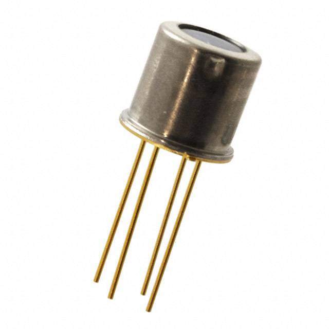
| 描述 | IC THERMOMETER IR 3V (MED) TO-39 |
| 产品分类 | 温度传感器,变送器 |
| 品牌 | Melexis Technologies NV |
| 数据手册 | http://www.melexis.com/Asset/IR-sensor-thermometer-MLX90614-Datasheet-DownloadLink-5152.aspxhttp://www.melexis.com/Asset/Flyer-MLX90614-DownloadLink-5083.aspx |
| 产品图片 |
|
| 产品型号 | MLX90614ESF-DCH-000-TU |
| rohs | 无铅 / 符合限制有害物质指令(RoHS)规范要求 |
| RoHS指令信息 | http://melexis.com/Asset/Green--Halogen-Free-Compliance-Declaration-MLX90614-DownloadLink-6153.aspx |
| 产品系列 | - |
| 供应商器件封装 | TO-39 |
| 其它名称 | MLX90614ESF-DCH |
| 包装 | 管件 |
| 封装/外壳 | TO-205AD、TO-39-4 改进型金属罐 |
| 感应温度 | -40°C ~ 125°C, -70°C ~ 380°C |
| 标准包装 | 49 |
| 特色产品 | http://www.digikey.cn/product-highlights/zh/mlx90614-infrared-thermometer/50282 |
| 电压-电源 | 2.6 V ~ 3.6 V |
| 精度 | ±1°C |
| 输出类型 | PWM,SMBus™ |


- 商务部:美国ITC正式对集成电路等产品启动337调查
- 曝三星4nm工艺存在良率问题 高通将骁龙8 Gen1或转产台积电
- 太阳诱电将投资9.5亿元在常州建新厂生产MLCC 预计2023年完工
- 英特尔发布欧洲新工厂建设计划 深化IDM 2.0 战略
- 台积电先进制程称霸业界 有大客户加持明年业绩稳了
- 达到5530亿美元!SIA预计今年全球半导体销售额将创下新高
- 英特尔拟将自动驾驶子公司Mobileye上市 估值或超500亿美元
- 三星加码芯片和SET,合并消费电子和移动部门,撤换高东真等 CEO
- 三星电子宣布重大人事变动 还合并消费电子和移动部门
- 海关总署:前11个月进口集成电路产品价值2.52万亿元 增长14.8%


PDF Datasheet 数据手册内容提取
MLX90614 family Datasheet Single and Dual Zone Infra Red Thermometer in TO-39 Features and Benefits Application Examples (cid:1) Small size, low cost (cid:1) High precision non-contact temperature (cid:1) Easy to integrate measurements (cid:1) Factory calibrated in wide temperature (cid:1) Thermal Comfort sensor for Mobile Air range: Conditioning control system (cid:1) -40°C…+125˚C for sensor temperature and (cid:1) Temperature sensing element for -70°C…+380˚C for object temperature. residential, commercial and industrial (cid:1) High accuracy of 0.5°C in a wide building air conditioning temperature range (0°C…+50°C for both Ta (cid:1) Windshield defogging and To) (cid:1) Automotive blind angle detection (cid:1) High (medical) accuracy calibration (cid:1) Industrial temperature control of moving (cid:1) Measurement resolution of 0.02°C parts (cid:1) Single and dual zone versions (cid:1) Temperature control in printers and (cid:1) SMBus compatible digital interface copiers (cid:1) Customizable PWM output for continuous (cid:1) Home appliances with temperature control reading (cid:1) Healthcare (cid:1) Available in 3V and 5V versions (cid:1) Livestock monitoring (cid:1) Simple adaptation for 8V…16V applications (cid:1) Movement detection (cid:1) Sleep mode for reduced power (cid:1) Multiple zone temperature control – up to consumption 127 sensors can be read via common 2 (cid:1) Different package options for applications wires and measurements versatility (cid:1) Thermal relay / alert (cid:1) Body temperature measurement (cid:1) Automotive grade Ordering Information Part No. Temperature Package - Option Code Standard Packing Code Code - X X X part form MLX90614 E (-40°C...85°C) SF (TO-39) (1) (2) (3) -000 -TU K (-40°C…125°C) (1) Supply Voltage/ Accuracy (2) Number of thermopiles: (3) Package options: A - 5V A – single zone A – Standard package B - 3V B – dual zone B – Reserved C - Reserved C – gradient compensated* C – 35° FOV D - 3V medical accuracy D/E – Reserved F – 10° FOV G – Reserved H – 12° FOV (refractive lens) I – 5° FOV K – 13°FOV Example: MLX90614ESF-BAA-000-TU * : See page 2 REVISION 11 - JUNE 15, 2017 3901090614
MLX90614 family Single and Dual Zone Infra Red Thermometer in TO-39 1. Functional diagram 2. General Description The MLX90614 is an Infra Red thermometer for non- MLX90614Axx: Vdd=4.5...5.5V contact temperature measurements. Both the IR J1 1 MLX90614 SCL U1 sensitive thermopile detector chip and the signal SCL Vz conditioning ASSP are integrated in the same TO-39 can. PWM 4 SDA 2SDA Vss Thanks to its low noise amplifier, 17-bit ADC and Vdd Vdd powerful DSP unit, a high accuracy and resolution of the C1 3 thermometer is achieved. GND CON1 0.1uF The thermometer comes factory calibrated with a digital C1 value and type may differ PWM and SMBus (System Management Bus) output. in different applications As a standard, the 10-bit PWM is configured to for optimum EMC continuously transmit the measured temperature in MLX90614 connection to SMBus range of -20…120˚C, with an output resolution of 0.14˚C. Figure 1: Typical application schematics The factory default POR setting is SMBus. The MLX90614 is built from 2 chips developed and manufactured by Melexis: (cid:1) The Infra Red thermopile detector MLX81101 (cid:1) The signal conditioning ASSP MLX90302, specially designed to process the output of IR sensor. The device is available in an industry standard TO-39 package. Thanks to the low noise amplifier, high resolution 17-bit ADC and powerful DSP unit of MLX90302 high accuracy and resolution of the thermometer is achieved. The calculated object and ambient temperatures are available in RAM of MLX90302 with resolution of 0.01°C. They are accessible by 2 wire serial SMBus compatible protocol (0.02°C resolution) or via 10-bit PWM (Pulse Width Modulated) output of the device. The MLX90614 is factory calibrated in wide temperature ranges: -40°C…125°C for the ambient temperature and -70°C…380°C for the object temperature. The measured value is the average temperature of all objects in the Field Of View of the sensor. The MLX90614 offers a standard accuracy of ±0.5˚C around room temperatures. A special version for medical applications exists offering an accuracy of ±0.2˚C in a limited temperature range around the human body temperature. It is very important for the application designer to understand that these accuracies are only guaranteed and achievable when the sensor is in thermal equilibrium and under isothermal conditions (there are no temperature differences across the sensor package). The accuracy of the thermometer can be influenced by temperature differences in the package induced by causes like (among others): Hot electronics behind the sensor, heaters/coolers behind or beside the sensor or by a hot/cold object very close to the sensor that not only heats the sensing element in the thermometer but also the thermometer package. This effect is especially relevant for thermometers with a small FOV like the xxC and xxF as the energy received by the sensor from the object is reduced. Therefore, Melexis has introduced the xCx version of the MLX90614. In these MLX90614xCx, the thermal gradients are measured internally and the measured temperature is compensated for them. In this way, the xCx version of the MLX90614 is much less sensitive to thermal gradients, but the effect is not totally eliminated. It is therefore important to avoid the causes of thermal gradients as much as possible or to shield the sensor from them. As a standard, the MLX90614 is calibrated for an object emissivity of 1. It can be easily customized by the customer for any other emissivity in the range 0.1…1.0 without the need of recalibration with a black body. The 10-bit PWM is as a standard configured to transmit continuously the measured object temperature for an object temperature range of -20°C…120°C with an output resolution of 0.14°C. The PWM can be easily customized for virtually any range desired by the customer by changing the content of 2 EEPROM cells. This has no effect on the factory calibration of the device. REVISION 11 - JUNE 15, 2017 3901090614
MLX90614 family Single and Dual Zone Infra Red Thermometer in TO-39 The PWM pin can also be configured to act as a thermal relay (input is To), thus allowing for an easy and cost effective implementation in thermostats or temperature (freezing / boiling) alert applications. The temperature threshold is user programmable. In a SMBus system this feature can act as a processor interrupt that can trigger reading all slaves on the bus and to determine the precise condition. The thermometer is available in 2 supply voltage options: 5V compatible or 3V (battery) compatible. The 5V can be easily adopted to operate from a higher supply voltage (8…16V, for example) by use of few external components (refer to “Applications information” section for details). An optical filter (long-wave pass) that cuts off the visible and near infra-red radiant flux is integrated in the package to provide ambient and sunlight immunity. The wavelength pass band of this optical filter is from 5.5…14µm (except for xCH and xCI type of devices which incorporate uncoated silicon lens). REVISION 11 - 20 NOVEMBER 2018 Page 3 of 57 3901090614
MLX90614 family Single and Dual Zone Infra Red Thermometer in TO-39 3. Contents FFFFeeeeaaaattttuuuurrrreeeessss aaaannnndddd BBBBeeeennnneeeeffffiiiittttssss ................................................................................................................................................................................................................................................................................................................................................................................................................................................................................................................................ 1111 AAAApppppppplllliiiiccccaaaattttiiiioooonnnn EEEExxxxaaaammmmpppplllleeeessss ................................................................................................................................................................................................................................................................................................................................................................................................................................................................................................................................ 1111 OOOOrrrrddddeeeerrrriiiinnnngggg IIIInnnnffffoooorrrrmmmmaaaattttiiiioooonnnn ................................................................................................................................................................................................................................................................................................................................................................................................................................................................................................................................ 1111 1111.... FFFFuuuunnnnccccttttiiiioooonnnnaaaallll ddddiiiiaaaaggggrrrraaaammmm ................................................................................................................................................................................................................................................................................................................................................................................................................................................................................................................................ 2222 2222.... GGGGeeeennnneeeerrrraaaallll DDDDeeeessssccccrrrriiiippppttttiiiioooonnnn ............................................................................................................................................................................................................................................................................................................................................................................................................................................................................................................................ 2222 3333.... CCCCoooonnnntttteeeennnnttttssss ................................................................................................................................................................................................................................................................................................................................................................................................................................................................................................................................................................................................ 4444 4444.... GGGGlllloooossssssssaaaarrrryyyy ooooffff TTTTeeeerrrrmmmmssss ........................................................................................................................................................................................................................................................................................................................................................................................................................................................................................................................................ 7777 5555.... MMMMaaaaxxxxiiiimmmmuuuummmm rrrraaaattttiiiinnnnggggssss .. .......................................................................................................................................................................................................................................................................................................................................................................................................................................................................................................................................... 7777 6666.... PPPPiiiinnnn ddddeeeeffffiiiinnnniiiittttiiiioooonnnnssss aaaannnndddd ddddeeeessssccccrrrriiiippppttttiiiioooonnnnssss .................................................................................................................................................................................................................................................................................................................................................................................................................................................... 8888 7777.... EEEElllleeeeccccttttrrrriiiiccccaaaallll SSSSppppeeeecccciiiiffffiiiiccccaaaattttiiiioooonnnnssss .................................................................................................................................................................................................................................................................................................................................................................................................................................................................................................... 9999 7.1. MLX90614Axx ..................................................................................................................................... 9 7.2. MLX90614Bxx, MLX90614Dxx .......................................................................................................... 11 8888.... DDDDeeeettttaaaaiiiilllleeeedddd ddddeeeessssccccrrrriiiippppttttiiiioooonnnn ................................................................................................................................................................................................................................................................................................................................................................................................................................................................................................................ 11113333 8.1. Block diagram .................................................................................................................................... 13 8.2. Signal processing principle ............................................................................................................... 13 8.3. Block description ............................................................................................................................... 14 8.3.1. Amplifier ...................................................................................................................................... 14 8.3.2. Supply regulator and POR .......................................................................................................... 14 8.3.3. EEPROM ...................................................................................................................................... 14 8.3.4. RAM ............................................................................................................................................. 17 8.4. SMBus compatible 2-wire protocol ................................................................................................. 17 8.4.1. Functional description ................................................................................................................ 17 8.4.2. Differences with the standard SMBus specification (reference [1]) ........................................ 18 8.4.3. Detailed description ................................................................................................................... 18 8.4.4. Bit transfer .................................................................................................................................. 19 8.4.5. Commands .................................................................................................................................. 20 8.4.6. SMBus communication examples .............................................................................................. 20 8.4.7. Timing specification .................................................................................................................... 21 8.4.8. Sleep Mode ................................................................................................................................. 22 8.4.9. MLX90614 SMBus specific remarks ........................................................................................... 23 8.5. PWM .................................................................................................................................................. 24 REVISION 11 - 20 NOVEMBER 2018 Page 4 of 57 3901090614
MLX90614 family Single and Dual Zone Infra Red Thermometer in TO-39 8.5.1. Single PWM format ..................................................................................................................... 25 8.5.2. Extended PWM format ............................................................................................................... 26 8.5.3. Customizing the temperature range for PWM output ............................................................. 27 8.6. Switching Between PWM / Thermal relay and SMBus communication ........................................ 29 8.6.1. PWM is enabled .......................................................................................................................... 29 8.6.2. Request condition ....................................................................................................................... 29 8.6.3. PWM is disabled ......................................................................................................................... 29 8.7. Computation of ambient and object temperatures ....................................................................... 30 8.7.1. Ambient temperature Ta ............................................................................................................ 30 8.7.2. Object temperature To ............................................................................................................... 30 8.7.3. Calculation flow .......................................................................................................................... 31 8.8. Thermal relay .................................................................................................................................... 32 9999.... UUUUnnnniiiiqqqquuuueeee FFFFeeeeaaaattttuuuurrrreeeessss ........................................................................................................................................................................................................................................................................................................................................................................................................................................................................................................................................ 33333333 11110000.... PPPPeeeerrrrffffoooorrrrmmmmaaaannnncccceeee GGGGrrrraaaapppphhhhssss........................................................................................................................................................................................................................................................................................................................................................................................................................................................................................................ 33334444 10.1. Temperature accuracy of the MLX90614 ...................................................................................... 34 10.1.1. Standard accuracy .................................................................................................................... 34 10.1.2. Medical accuracy ...................................................................................................................... 36 10.1.3. Temperature reading dependence on VDD ............................................................................ 36 10.2. Field Of View (FOV) ......................................................................................................................... 38 11111111.... AAAApppppppplllliiiiccccaaaattttiiiioooonnnnssss IIIInnnnffffoooorrrrmmmmaaaattttiiiioooonnnn ............................................................................................................................................................................................................................................................................................................................................................................................................................................................................ 44442222 11.1. Use of the MLX90614 thermometer in SMBus configuration ...................................................... 42 11.2. Use of multiple MLX90614s in SMBus configuration ................................................................... 42 11.3. PWM output operation .................................................................................................................. 42 11.4. Thermal alert / thermostat ............................................................................................................ 43 11.5. High voltage source operation ....................................................................................................... 44 11112222.... AAAApppppppplllliiiiccccaaaattttiiiioooonnnn CCCCoooommmmmmmmeeeennnnttttssss ........................................................................................................................................................................................................................................................................................................................................................................................................................................................................................ 44445555 11113333.... SSSSttttaaaannnnddddaaaarrrrdddd iiiinnnnffffoooorrrrmmmmaaaattttiiiioooonnnn rrrreeeeggggaaaarrrrddddiiiinnnngggg mmmmaaaannnnuuuuffffaaaaccccttttuuuurrrraaaabbbbiiiilllliiiittttyyyy ooooffff MMMMeeeelllleeeexxxxiiiissss pppprrrroooodddduuuuccccttttssss wwwwiiiitttthhhh ddddiiiiffffffffeeeerrrreeeennnntttt ssssoooollllddddeeeerrrriiiinnnngggg pppprrrroooocccceeeesssssssseeeessss ................................................................................................................................................................................................................................................................................................................................................................................................................................................................................................................................................................................ 44447777 11114444.... EEEESSSSDDDD PPPPrrrreeeeccccaaaauuuuttttiiiioooonnnnssss .. .................................................................................................................................................................................................................................................................................................................................................................................................................................................................................................................................. 44447777 11115555.... FFFFAAAAQQQQ ............................................................................................................................................................................................................................................................................................................................................................................................................................................................................................................................................................................................................ 44448888 11116666.... PPPPaaaacccckkkkaaaaggggeeee IIIInnnnffffoooorrrrmmmmaaaattttiiiioooonnnn .. ...................................................................................................................................................................................................................................................................................................................................................................................................................................................................................................... 55550000 16.1. MLX90614xxA ................................................................................................................................. 50 16.2. MLX90614xCC ................................................................................................................................. 50 REVISION 11 - 20 NOVEMBER 2018 Page 5 of 57 3901090614
MLX90614 family Single and Dual Zone Infra Red Thermometer in TO-39 16.3. MLX90614xCF ................................................................................................................................. 51 16.4. MLX90614xCH ................................................................................................................................. 51 16.5. MLX90614xCI .................................................................................................................................. 52 16.6. MLX90614xCK ................................................................................................................................. 52 16.7. Part marking .................................................................................................................................... 53 16.8. Operating and storage humidity range ......................................................................................... 53 11117777.... TTTTaaaabbbblllleeee ooooffff ffffiiiigggguuuurrrreeeessss ........................................................................................................................................................................................................................................................................................................................................................................................................................................................................................................................................ 55554444 11118888.... RRRReeeeffffeeeerrrreeeennnncccceeeessss.................................................................................................................................................................................................................................................................................................................................................................................................................................................................................................................................................................... 55555555 11119999.... CCCCoooonnnnttttaaaacccctttt ........................................................................................................................................................................................................................................................................................................................................................................................................................................................................................................................................................................................ 55556666 22220000.... DDDDiiiissssccccllllaaaaiiiimmmmeeeerrrr ........................................................................................................................................................................................................................................................................................................................................................................................................................................................................................................................................................................ 55556666 REVISION 11 - 20 NOVEMBER 2018 Page 6 of 57 3901090614
MLX90614 family Single and Dual Zone Infra Red Thermometer in TO-39 4. Glossary of Terms PTAT Proportional To Absolute Temperature sensor (package temperature) POR Power On Reset HFO High Frequency Oscillator (RC type) DSP Digital Signal Processing FIR Finite Impulse Response. Digital filter IIR Infinite Impulse Response. Digital filter IR Infra-Red PWM Pulse With Modulation DC Duty Cycle (of the PWM) ; Direct Current (for settled conditions specifications) FOV Field Of View SDA,SCL Serial DAta, Serial CLock – SMBus compatible communication pins Ta Ambient Temperature measured from the chip – (the package temperature) To Object Temperature, ‘seen’ from IR sensor ESD Electro-Static Discharge EMC Electro-Magnetic Compatibility ASSP Application Specific Standard Product TBD To Be Defined Note: sometimes the MLX90614xxx is referred as “the module”. 5. Maximum ratings Parameter MLX90614ESF-Axx MLX90614ESF-Bxx MLX90614KSF-Axx MLX90614ESF-Dxx Supply Voltage, V (over voltage) 7V 5V 7V DD Supply Voltage, V (operating) 5.5 V 3.6V 5.5V DD Reverse Voltage 0.4 V Operating Temperature Range, T -40°C…+85°C -40°C…+125°C A Storage Temperature Range, T -40°C…+125°C -40°C…+125°C S ESD Sensitivity (AEC Q100 002) 2kV DC current into SCL / Vz (Vz mode) 2 mA DC sink current, SDA / PWM pin 25 mA DC source current, SDA / PWM pin 25 mA DC clamp current, SDA / PWM pin 25 mA DC clamp current, SCL pin 25 mA Table 1: Absolute maximum ratings for MLX90614 Exceeding the absolute maximum ratings may cause permanent damage. Exposure to absolute-maximum-rated conditions for extended periods may affect device reliability. REVISION 11 - 20 NOVEMBER 2018 Page 7 of 57 3901090614
MLX90614 family Single and Dual Zone Infra Red Thermometer in TO-39 6. Pin definitions and descriptions 4 - VSS 1 - SCL / Vz 3 - VDD 2 - SDA / PWM Bottom view Figure 2: Pin description Pin Name Function Serial clock input for 2 wire communications protocol. 5.7V zener is available at SCL / Vz this pin for connection of external bipolar transistor to MLX90614Axx to supply the device from external 8…16V source. Digital input / output. In normal mode the measured object temperature is available at this pin Pulse Width Modulated. SDA / PWM In SMBus compatible mode the pin is automatically configured as open drain NMOS. VDD External supply voltage. VSS Ground. The metal can is also connected to this pin. Table 2: Pin description MLX90614 Note: for +12V (+8…+16V) powered operation refer to the Application information section. For EMC and isothermal conditions reasons it is highly recommended not to use any electrical connection to the metal can except by the VSS pin. With the SCL / Vz and PWM / SDA pins operated in 2-wire interface mode, the input Schmidt trigger function is automatically enabled. REVISION 11 - 20 NOVEMBER 2018 Page 8 of 57 3901090614
MLX90614 family Single and Dual Zone Infra Red Thermometer in TO-39 7. Electrical Specifications 7777....1111.... MMMMLLLLXXXX99990000666611114444AAAAxxxxxxxx All parameters are valid for T = 25 ˚C, V =5V (unless otherwise specified) A DD Parameter Symbol Test Conditions Min Typ Max Units Supplies External supply V 4.5 5 5.5 V DD Supply current I No load 1.3 2 mA DD Supply current No load, erase/write EEPROM I 1.5 2.5 mA (programming) DDpr operations Zener voltage Vz Iz = 75…1000μA (Ta=room) 5.5 5.7 5.9 V Iz = 70…1000μA, Zener voltage Vz(Ta) 5.15 5.7 6.24 V full temperature range Power On Reset POR level V Power-up (full temp range) 1.4 1.75 1.95 V POR_up POR level V Power –down (full temp range) 1.3 1.7 1.9 V POR_down POR hysteresis V Full temp range 0.08 0.1 1.15 V POR_hys V rise time (10% to 90% of DD T Ensure POR signal 20 ms specified supply voltage) POR Output valid Tvalid After POR 0.25 s (result in RAM) Pulse width modulation1 PWM resolution PWMres Data band 10 bit Factory default, internal oscillator PWM output period PWM 1.024 ms T,def factory calibrated Internal oscillator factory PWM period stability dPWM calibrated, over the entire -10 +10 % T operation range and supply voltage Output high Level PWM I = 2 mA V -0.2 V HI source DD Output low Level PWM I = 2 mA V +0.2 V LO sink SS Output drive current Idrive Vout,H = V - 0.8V 7 mA PWM DD Output sink current Isink Vout,L = 0.8V 13.5 mA PWM Continued on next page REVISION 11 - 20 NOVEMBER 2018 Page 9 of 57 3901090614
MLX90614 family Single and Dual Zone Infra Red Thermometer in TO-39 Parameter Symbol Test Conditions Min Typ Max Units SMBus compatible 2-wire interface2 Input high voltage V (Ta, V) Over temperature and supply 3 V IH Input low voltage V (Ta, V) Over temperature and supply 0.6 V IL Over temperature and supply, Isink Output low voltage V 0.2 V OL = 2mA SCL leakage I , leak V =4V, Ta=+85°C 30 μA SCL SCL SDA leakage I , leak V =4V, Ta=+85°C 0.3 μA SDA SDA SCL capacitance C 10 pF SCL SDA capacitance C 10 pF SDA Slave address SA Factory default 5A hex Wake up request t SDA low 33 ms wake SMBus Request t SCL low 1.44 ms REQ Timeout, low T SCL low 27 33 ms imeout,L Timeout, high T SCL high 45 55 μs imeout,H Acknowledge setup time Tsuac(MD) 8-th SCL falling edge, Master 1.5 μs Acknowledge hold time Thdac(MD) 9-th SCL falling edge, Master 1.5 μs Acknowledge setup time Tsuac(SD) 8-th SCL falling edge, Slave 2.5 μs Acknowledge hold time Thdac(SD) 9-th SCL falling edge, Slave 1.5 μs EEPROM Data retention Ta = +85°C 10 years Erase/write cycles Ta = +25°C 100,000 Times Erase/write cycles Ta = +125°C 10,000 Times Erase cell time Terase 5 ms Write cell time Twrite 5 ms Table 3: Electrical specification MLX90614Axx Notes: All the communication and refresh rate timings are given for the nominal calibrated HFO frequency and will vary with this frequency’s variations. 1. With large capacitive load lower PWM frequency is recommended. Thermal relay output (when configured) has the PWM DC specification and can be programmed as push-pull, or NMOS open drain. PWM is free-running, power-up factory default is SMBus, refer to section 8.6, “Switching between PWM and SMBus communication” for more details. 2. For SMBus compatible interface on 12V application refer to Application information section. SMBus compatible interface is described in details in the SMBus detailed description section. Maximum number of MLX90614 devices on one bus is 127, higher pull-up currents are recommended for higher number of devices, faster bus data transfer rates, and increased reactive loading of the bus. MLX90614 is always a slave device on the bus. MLX90614 can work in both low-power and high-power SMBus communication. All voltages are referred to the Vss (ground) unless otherwise noted. Sleep mode is not available on the 5V version (MLX90614Axx). REVISION 11 - 20 NOVEMBER 2018 Page 10 of 57 3901090614
MLX90614 family Single and Dual Zone Infra Red Thermometer in TO-39 7777....2222.... MMMMLLLLXXXX99990000666611114444BBBBxxxxxxxx,,,, MMMMLLLLXXXX99990000666611114444DDDDxxxxxxxx All parameters are valid for T = 25 ˚C, V =3V (unless otherwise specified) A DD Parameter Symbol Test Conditions Min Typ Max Units Supplies External supply V 2.6 3 3.6 V DD Supply current I No load 1.3 2 mA DD Supply current No load, erase / write EEPROM I 1.5 2.5 mA (programming) DDpr operations Sleep mode current Isleep no load 1 2.5 5 μA Sleep mode current Isleep Full temperature range 1 2.5 6 μA Power On Reset POR level V Power-up (full temp range) 1.4 1.75 1.95 V POR_up POR level V Power –down (full temp range) 1.3 1.7 1.9 V POR_down POR hysteresis V Full temp range 0.08 0.1 1.15 V POR_hys V rise time DD (10% to 90% of T Ensure POR signal 20 ms POR specified supply voltage) Output valid Tvalid After POR 0.25 s Pulse width modulation1 PWM resolution PWMres Data band 10 bit Factory default, internal oscillator PWM output period PWM 1.024 ms T,def factory calibrated Internal oscillator factory PWM period stability dPWM calibrated, over the entire -10 +10 % T operation range and supply voltage Output high Level PWM I = 2 mA V -0.25 V HI source DD Output low Level PWM I = 2 mA V +0.25 V LO sink SS Output drive current Idrive Vout,H = V - 0.8V 4.5 mA PWM DD Output sink current Isink Vout,L = 0.8V 11 mA PWM Continued on next page REVISION 11 - 20 NOVEMBER 2018 Page 11 of 57 3901090614
MLX90614 family Single and Dual Zone Infra Red Thermometer in TO-39 Parameter Symbol Test Conditions Min Typ Max Units SMBus compatible 2-wire interface2 Input high voltage V (Ta,V) Over temperature and supply VDD-0.1 V IH Input low voltage V (Ta,V) Over temperature and supply 0.6 V IL Over temperature and supply, Output low voltage V 0.25 V OL Isink = 2mA SCL leakage I ,leak V =3V, Ta=+85°C 20 μA SCL SCL SDA leakage I ,leak V =3V, Ta=+85°C 0.25 μA SDA SDA SCL capacitance C 10 pF SCL SDA capacitance C 10 pF SDA Slave address SA Factory default 5A hex Wake up request t SDA low 33 ms wake SMBus Request t SCL low 1.44 ms REQ Timeout,low T SCL low 27 33 ms imeout,L Timeout, high T SCL high 45 55 μs imeout,H Acknowledge setup time Tsuac(MD) 8-th SCL falling edge, Master 1.5 μs Acknowledge hold time Thdac(MD) 9-th SCL falling edge, Master 1.5 μs Acknowledge setup time Tsuac(SD) 8-th SCL falling edge, Slave 2.5 μs Acknowledge hold time Thdac(SD) 9-th SCL falling edge, Slave 1.5 μs EEPROM Data retention Ta = +85°C 10 years Erase/write cycles Ta = +25°C 100,000 Times Erase/write cycles Ta = +125°C 10,000 Times Erase cell time Terase 5 ms Write cell time Twrite 5 ms Table 4: Electrical specification MLX90614Bxx, Dxx Note: refer to MLX90614Axx notes. REVISION 11 - 20 NOVEMBER 2018 Page 12 of 57 3901090614
MLX90614 family Single and Dual Zone Infra Red Thermometer in TO-39 8. Detailed description 8888....1111.... BBBBlllloooocccckkkk ddddiiiiaaaaggggrrrraaaammmm 81101 OPA ADC DSP PWM t° STATE MACHINE Voltage 90302 Regulator Figure 3: Block diagram 8888....2222.... SSSSiiiiggggnnnnaaaallll pppprrrroooocccceeeessssssssiiiinnnngggg pppprrrriiiinnnncccciiiipppplllleeee The operation of the MLX90614 is controlled by an internal state machine, which controls the measurements and calculations of the object and ambient temperatures and does the post-processing of the temperatures to output them through the PWM output or the SMBus compatible interface. The ASSP supports 2 IR sensors (second one not implemented in the MLX90614xAx).The output of the IR sensors is amplified by a low noise low offset chopper amplifier with programmable gain, converted by a Sigma Delta modulator to a single bit stream and fed to a powerful DSP for further processing. The signal is treated by programmable (by means of EEPROM contend) FIR and IIR low pass filters for further reduction of the band width of the input signal to achieve the desired noise performance and refresh rate. The output of the IIR filter is the measurement result and is available in the internal RAM. 3 different cells are available: One for the on-board temperature sensor and 2 for the IR sensors. Based on results of the above measurements, the corresponding ambient temperature Ta and object temperatures To are calculated. Both calculated temperatures have a resolution of 0.01˚C. The data for Ta and To can be read in two ways: Reading RAM cells dedicated for this purpose via the 2-wire interface (0.02°C resolution, fixed ranges), or through the PWM digital output (10 bit resolution, configurable range). In the last step of the measurement cycle, the measured Ta and To are rescaled to the desired output resolution of the PWM) and the recalculated data is loaded in the registers of the PWM state machine, which creates a constant frequency with a duty cycle representing the measured data. REVISION 11 - 20 NOVEMBER 2018 Page 13 of 57 3901090614
MLX90614 family Single and Dual Zone Infra Red Thermometer in TO-39 8888....3333.... BBBBlllloooocccckkkk ddddeeeessssccccrrrriiiippppttttiiiioooonnnn 8888....3333....1111.... AAAAmmmmpppplllliiiiffffiiiieeeerrrr A low noise, low offset amplifier with programmable gain is used for amplifying the IR sensor voltage. By carefully designing the input modulator and balanced input impedance, the max offset of the system is 0.5μV. 8888....3333....2222.... SSSSuuuuppppppppllllyyyy rrrreeeegggguuuullllaaaattttoooorrrr aaaannnndddd PPPPOOOORRRR The module can operate from 3 different supplies: VDD = 5V (cid:2) MLX90614Axx VDD = 3V (cid:2) MLX90614Bxx (battery or regulated supply) VDD = 8V…16V (cid:2) MLX90614Axx few external components are necessary please refer to “Applications information” section for information about adopting higher voltage supplies. The Power On Reset (POR) is connected to Vdd supply. The on-chip POR circuit provides an active (high) level of the POR signal when the Vdd voltage rises above approximately 0.5V and holds the entire MLX90614 in reset until the Vdd is higher than the specified POR threshold V . During the time POR is active, the POR signal is available as an open drain at the POR PWM/SDA pin. After the MLX90614 exits the POR condition, the function programmed in EEPROM takes precedence for that pin. 8888....3333....3333.... EEEEEEEEPPPPRRRROOOOMMMM A limited number of addresses in the EEPROM memory can be changed by the customer. The whole EEPROM can be read through the SMBus interface. EEPROM (32X16) Name Address Write access To 0x00 Yes max To 0x01 Yes min PWMCTRL 0x02 Yes Ta range 0x03 Yes Emissivity correction coefficient 0x04 Yes Config Register1 0x05 Yes Melexis reserved 0x06 No … … … Melexis reserved 0x0D No SMBus address (LSByte only) 0x0E Yes Melexis reserved 0x0F Yes Melexis reserved 0x10 No … … … Melexis reserved 0x18 No Melexis reserved 0x19 Yes Melexis reserved 0x1A No Melexis reserved 0x1B No ID number 0x1C No ID number 0x1D No ID number 0x1E No ID number 0x1F No Table 5: EEPROM table The addresses To , To and Ta range are for customer dependent object and ambient temperature ranges. For details see max min section 8.5.3 below in this document The address Emissivity contains the object emissivity (factory default 1.0 = 0xFFFF), 16 bit. ε Emissivity = dec2hex[ round( 65535 x ) ] Where dec2hex[ round( X ) ] represents decimal to hexadecimal conversion with round-off to nearest value (not truncation). ε In this case the physical emissivity values are = 0.1…1.0. Erase (write 0) must take place before write of desired data is made. REVISION 11 - 20 NOVEMBER 2018 Page 14 of 57 3901090614
MLX90614 family Single and Dual Zone Infra Red Thermometer in TO-39 PWM period configuration: Period in extended PWM mode is twice the period in single PWM mode. In single PWM mode period is T = 1.024*P [ms], where P is the number, written in bits 15…9 PWMCTRL. Maximum period is then 131.072 ms for single and 262.144 ms for extended. These values are typical and depend on the on-chip RC oscillator absolute value. The duty cycle must be calculated instead of working only with the high time only in order to avoid errors from the period absolute value deviations. The address PWMCTRL consists of control bits for configuring the PWM/SDA pin as follows: 15 14 13 12 11 10 9 8 7 6 5 4 3 2 1 0 PWM control bit meaning 0 - PWM extended mode 1 - PWM single mode 0 - PWM mode disabled (EN_PWM) 1 - PWM mode enabled (EN_PWM) 0 - SDA pin configured as Open Drain (PPODB) 1 - SDA pin configured as Push-Pull (PPODB) 0 - PWM mode selected (TRPWMB) 1 - Thermal relay mode selected (TRPWMB) - PWM repetition number 0…62 step 2 - PWM period 1.024*ms (Single PWM mode) or 2.048*ms (Extendet PWM mode) multiplied by the number written in this place (128 in case the number is 0) * Values are valid for nominal HFO frequency Table 6: PWM control bits The address ConfigRegister1 consists of control bits for configuring the analog and digital parts: 15 14 13 12 11 10 9 8 7 6 5 4 3 2 1 0 Config register bit meaning 1 0 0 - IIR (100%) a1=1, b1=0 1 0 1 - IIR (80%) a1=0.8, b1=0.2 1 1 0 - IIR (67%) a1=0.666, b1=0.333 1 1 1 - IIR (57%) a1=0.571, b1=0.428 0 0 0 - IIR (50%) a1=0.5, b1=0.5 0 0 1 - IIR (25%) a1=0.25, b1=0.75 0 1 0 - IIR (17%) a1=0.166(6), b1=0.83(3) 0 1 1 - IIR (13%) a1=0.125, b1=0.875 0 - Repeat sensor test "OFF" 1 - Repeat sensor test "ON" 0 0 - Ta, Tobj1 0 1 - Ta, Tobj2 1 0 - Tobj2 1 1 - Tobj1, Tobj2 0 - Single IR sensor 1 - Dual IR sensor 0 - Positive sign of Ks 1 - Negative sign of Ks 0 0 0 - FIR = 8 not recommended 0 0 1 - FIR = 16 not recommended 0 1 0 - FIR = 32 not recommended 0 1 1 - FIR = 64 not recommended 1 0 0 - FIR = 128 1 0 1 - FIR = 256 1 1 0 - FIR = 512 1 1 1 - FIR = 1024 0 0 0 - GAIN = 1 - Amplifier is bypassed 0 0 1 - GAIN = 3 0 1 0 - GAIN = 6 0 1 1 - GAIN = 12,5 1 0 0 - GAIN = 25 1 0 1 - GAIN = 50 1 1 0 - GAIN = 100 1 1 1 - GAIN = 100 0 - Positive sign of Kt2 1 - Negative sign of Kt2 0 - Enable sensor test 1 - Disable sensor test Note: The following bits / registers should not be altered (except with special tools – contact Melexis for such tools availability) in order to keep the factory calibration relevant: Ke [15...0]; Config Register1 [14...11;7;3]; addresses 0x0F and 0x19. Table 7: Configuration register 1 Check www.melexis.com for latest application notes with details on EEPROM settings. REVISION 11 - 20 NOVEMBER 2018 Page 15 of 57 3901090614
MLX90614 family Single and Dual Zone Infra Red Thermometer in TO-39 On-chip filtering and settling time: The MLX90614 features configurable on-chip digital filters. They allow customization for speed or noise. Factory default configurations and the typical settling time and noise for the MLX90614 family are given below. Device Settling time, sec Typical noise, °C rms Spike limit MLX90614AAA, BAA, DAA 0.10 0.05 100% MLX90614ABA, BBA 0.14 0.07 100% MLX90614ACC, BCC, DCC 0.14 0.18 100% MLX90614ACF, BCF 1.33 0.10 50% MLX90614DCH, DCI, BCH, BCI 0.65 0.10 80% MLX90614ACK, BCK 3.23 0.30 25% Table 8: factory default IIR and FIR configuration, settling time and typical noise Details on the filters are given in the application note “Understanding MLX90614 on-chip digital signal filters” available from www.melexis.com. The evaluation board, EVB90614 supported by PC SW allows easy configuration of the filters, while not requiring in-depth understanding of the EEPROM. The available filter settings and the settling times are listed below. Settling time depends on three configurations: single / dual zone, IIR filter settings and FIR filter settings. The FIR filter has a straight forward effect on noise (4 times decreasing of filter strength increases the noise 2 times and vice versa). The IIR filter provides an additional, spike limiting feature. Spike limit defines the level of magnitude to which the spike would be limited – for example, 25% denotes that if a 20°C temperature delta spike is measured the temperature reading by the MLX90614 will spike only 5°C. Settling time (s) Settling time (s) IIR setting FIR setting Spike limit 90614xAx 90614xBx, 90614xCx xxx 000…011 Not recommended 100 100 0.04 0.06 100.00% 100 101 0.05 0.07 100.00% 100 110 0.06 0.10 100.00% 100 111 0.10 0.14 100.00% 101 100 0.12 0.20 80.00% 101 101 0.16 0.24 80.00% 101 110 0.22 0.34 80.00% 101 111 0.35 0.54 80.00% 110 100 0.24 0.38 66.70% 110 101 0.30 0.48 66.70% 110 110 0.43 0.67 66.70% 110 111 0.70 1.10 66.70% 111 100 0.26 0.42 57.00% 111 101 0.34 0.53 57.00% 111 110 0.48 0.75 57.00% 111 111 0.78 1.20 57.00% 000 100 0.30 0.47 50.00% 000 101 0.37 0.60 50.00% 000 110 0.54 0.84 50.00% 000 111 0.86 1.33 50.00% 001 100 0.70 1.10 25.00% 001 101 0.88 1.40 25.00% 001 110 1.30 2.00 25.00% 001 111 2.00 3.20 25.00% 010 100 1.10 1.80 16.70% 010 101 1.40 2.20 16.70% 010 110 2.00 3.20 16.70% 010 111 3.30 5.00 16.70% 011 100 1.50 2.40 12.50% 011 101 1.90 3.00 12.50% 011 110 2.80 4.30 12.50% 011 111 4.50 7.00 12.50% Table 9: possible IIR and FIR settings Note: Settling time is in seconds and depends on internal oscillator absolute value. 100% spike limit appears with the IIR filter bypassed, and there is no spike limitation. REVISION 11 - 20 NOVEMBER 2018 Page 16 of 57 3901090614
MLX90614 family Single and Dual Zone Infra Red Thermometer in TO-39 8888....3333....4444.... RRRRAAAAMMMM It is not possible to write into the RAM memory. It can only be read and only a limited number of RAM registers are of interest to the customer. RAM (32x16) Name Address Read access Melexis reserved 0x00 Yes … … … Melexis reserved 0x03 Yes Raw data IR channel 1 0x04 Raw data IR channel 2 0x05 T 0x06 Yes A T 0x07 Yes OBJ1 T 0x08 Yes OBJ2 Melexis reserved 0x09 Yes … … … Melexis reserved 0x1F Yes Table 10: Ram addresses 8888....4444.... SSSSMMMMBBBBuuuussss ccccoooommmmppppaaaattttiiiibbbblllleeee 2222----wwwwiiiirrrreeee pppprrrroooottttooooccccoooollll The chip supports a 2 wires serial protocol, build with pins PWM / SDA and SCL. (cid:1) SCL – digital input only, used as the clock for SMBus compatible communication. This pin has the auxiliary function for building an external voltage regulator. When the external voltage regulator is used, the 2-wire protocol is available only if the power supply regulator is overdriven. (cid:1) PWM/SDA – Digital input / output, used for both the PWM output of the measured object temperature(s) or the digital input / output for the SMBus. In PWM mode the pin can be programmed in EEPROM to operate as Push / Pull or open drain NMOS (open drain NMOS is factory default). In SMBus mode SDA is forced to open drain NMOS I/O, push-pull selection bit defines PWM / Thermal relay operation. SMBus communication with MLX90614 is covered in details in application notes, available from www.melexis.com. 8888....4444....1111.... FFFFuuuunnnnccccttttiiiioooonnnnaaaallll ddddeeeessssccccrrrriiiippppttttiiiioooonnnn The SMBus interface is a 2-wire protocol, allowing communication between the Master Device (MD) and one or more Slave Devices (SD). In the system only one master can be presented at any given time [1]. The MLX90614 can only be used as a slave device. Generally, the MD initiates the start of data transfer by selecting a SD through the Slave Address (SA). The MD has read access to the RAM and EEPROM and write access to 9 EEPROM cells (at addresses 0x00, 0x01, 0x02, 0x03, 0x04, 0x05*, 0x0E, 0x0F, 0x19). If the access to the MLX90614 is a read operation it will respond with 16 data bits and 8 bit PEC only if its own slave address, programmed in internal EEPROM, is equal to the SA, sent by the master. The SA feature allows connecting up to 127 devices (SA=0x00…0x07F) with only 2 wires, unless the system has some of the specific features described in paragraph 5.2 of reference [1]. In order to provide access to any device or to assign an address to a SD before it is connected to the bus system, the communication must start with zero SA followed by low R/W¯ bit. When this command is sent from the MD, the MLX90614 will always respond and will ignore the internal chip code information. Special care must be taken not to put two MLX90614 devices with the same SA on the same bus as MLX90614 does not support ARP [1]. The MD can force the MLX90614 into low consumption mode “sleep mode” (3V version only). Read flags like “EEBUSY” (1 – EEPROM is busy with executing the previous write/erase), “EE_DEAD” (1 – there is fatal EEPROM error and this chip is not functional**). Note*: This address is readable and writable. Bit 3 should not be altered as this will cancel the factory calibration. Note**: EEPROM error signaling is implemented in automotive grade parts only. REVISION 11 - 20 NOVEMBER 2018 Page 17 of 57 3901090614
MLX90614 family Single and Dual Zone Infra Red Thermometer in TO-39 8888....4444....2222.... DDDDiiiiffffffffeeeerrrreeeennnncccceeeessss wwwwiiiitttthhhh tttthhhheeee ssssttttaaaannnnddddaaaarrrrdddd SSSSMMMMBBBBuuuussss ssssppppeeeecccciiiiffffiiiiccccaaaattttiiiioooonnnn ((((rrrreeeeffffeeeerrrreeeennnncccceeee [[[[1111]]]])))) There are eleven command protocols for standard SMBus interface. The MLX90614 supports only two of them. Not supported commands are: (cid:1) Quick Command (cid:1) Byte commands - Sent Byte, Receive Byte, Write Byte and Read Byte (cid:1) Process Call (cid:1) Block commands – Block Write and Write-Block Read Process Call Supported commands are: (cid:1) Read Word (cid:1) Write Word 8888....4444....3333.... DDDDeeeettttaaaaiiiilllleeeedddd ddddeeeessssccccrrrriiiippppttttiiiioooonnnn The PWM / SDA pin of MLX90614 can operate also as PWM output, depending on the EEPROM settings. If PWM is enabled, after POR the PWM / SDA pin is directly configured as PWM output. Even if the device is in PWM mode SMBus communication may be restored by a special command. That is why hereafter both modes are treated separately. 8888....4444....3333....1111.... BBBBuuuussss PPPPrrrroooottttooooccccoooollll 1 7 1 1 8 1 1 S Slave Address Wr A Data Byte A P S Start Condition Sr Repeated Start Condition Rd Read (bit value of 1) Wr Write (bit value of 0) A Acknowledge (this bit can be 0 for ACK and 1 for NACK) S Stop Condition PEC Packet Error Code Master-to-Slave Slave-to-Master Figure 4: SMBus packet element key After every received 8 bits the SD should issue ACK or NACK. When a MD initiates communication, it first sends the address of the slave and only the SD which recognizes the address will ACK, the rest will remain silent. In case the SD NACKs one of the bytes, the MD should stop the communication and repeat the message. A NACK could be received after the PEC. This means that there is an error in the received message and the MD should try sending the message again. The PEC calculation includes all bits except the START, REPEATED START, STOP, ACK, and NACK bits. The PEC is a CRC-8 with polynomial X8+X2+X1+1. The Most Significant Bit of every byte is transferred first. REVISION 11 - 20 NOVEMBER 2018 Page 18 of 57 3901090614
MLX90614 family Single and Dual Zone Infra Red Thermometer in TO-39 8888....4444....3333....1111....1111.... RRRReeeeaaaadddd WWWWoooorrrrdddd ((((ddddeeeeppppeeeennnnddddiiiinnnngggg oooonnnn tttthhhheeee ccccoooommmmmmmmaaaannnndddd –––– RRRRAAAAMMMM oooorrrr EEEEEEEEPPPPRRRROOOOMMMM)))) 1 7 1 1 8 1 1 7 1 1 S Slave Address Wr A Command A Sr Slave Address Rd A ……….. 8 1 8 1 8 1 1 ……….. Data Byte Low A Data Byte High A PEC A P Figure 5: SMBus read word format 8888....4444....3333....1111....2222.... WWWWrrrriiiitttteeee WWWWoooorrrrdddd ((((ddddeeeeppppeeeennnnddddiiiinnnngggg oooonnnn tttthhhheeee ccccoooommmmmmmmaaaannnndddd –––– RRRRAAAAMMMM oooorrrr EEEEEEEEPPPPRRRROOOOMMMM)))) 1 7 1 1 8 1 S Slave Address Wr A Command A ……….. 8 1 8 1 8 1 1 ……….. Data Byte Low A Data Byte High A PEC A P Figure 6: SMBus write word format 8888....4444....4444.... BBBBiiiitttt ttttrrrraaaannnnssssffffeeeerrrr Changing data SDA SCL Sampling data Figure 7: Recommended timing on SMBus The data on PWM / SDA must be changed when SCL is low (min 300ns after the falling edge of SCL). The data is fetched by both MD and SDs on the rising edge of the SCL. The recommended timing for changing data is in the middle of the period when the SCL is low. REVISION 11 - 20 NOVEMBER 2018 Page 19 of 57 3901090614
MLX90614 family Single and Dual Zone Infra Red Thermometer in TO-39 8888....4444....5555.... CCCCoooommmmmmmmaaaannnnddddssss RAM and EEPROM can be read both with 32x16 sizes. If the RAM is read, the data are divided by two, due to a sign bit in RAM (for example, T - RAM address 0x07 will sweep between 0x27AD to 0x7FFF as the object temperature changes from - O1 70.01°C…+382.19°C). The MSB read from RAM is an error flag (active high) for the linearized temperatures (TO1, TO2 and Ta). The MSB for the raw data (e.g. IR sensor1 data) is a sign bit (sign and magnitude format). A write of 0x0000 must be done prior to writing in EEPROM in order to erase the EEPROM cell content. Refer to EEPROM detailed description for factory calibration EEPROM locations that need to be kept unaltered. Opcode Command 000x xxxx* RAM Access 001x xxxx* EEPROM Access 1111_0000** Read Flags 1111_1111 Enter SLEEP mode Table 11: SMBus commands Note*: The xxxxx represent the 5 LSBits of the memory map address to be read / written. Note**: Behaves like read command. The MLX90614 returns PEC after 16 bits data of which only 4 are meaningful and if the MD wants it, it can stop the communication after the first byte. The difference between read and read flags is that the latter does not have a repeated start bit. Flags read are: Data[7] - EEBUSY - the previous write/erase EEPROM access is still in progress. High active. Data[6] - Unused Data[5] - EE_DEAD - EEPROM double error has occurred. High active. Data[4] - INIT - POR initialization routine is still ongoing. Low active. Data[3] - Not implemented. Data[2...0] and Data[8...15] - All zeros. Flag read is a diagnostic feature. The MLX90614 can be used regardless of these flags. For details and examples for SMBus communication with the MLX90614 check the www.melexis.com 8888....4444....6666.... SSSSMMMMBBBBuuuussss ccccoooommmmmmmmuuuunnnniiiiccccaaaattttiiiioooonnnn eeeexxxxaaaammmmpppplllleeeessss SA_W = 0xB4 Command = 0x07 SA_R = 0xB5 LSByte = 0xD2 MSByte = 0x3A PEC = 0x30 SDA S1 0 1 1 0 1 0 WA 0 0 0 0 0 1 1 1 A S1 0 1 1 0 1 0 R A 1 1 0 1 0 0 1 0 A 0 0 1 1 1 0 1 0 A 0 0 1 1 0 0 0 0 A P SCL Figure 8: Read word format (SA=0x5A, read RAM=0x07, result=0x3AD2, PEC=0x30) SA_W = 0xB4 Command = 0x22 LSByte = 0x07 MSByte = 0xC8 PEC = 0x48 SDA S1 0 1 1 0 1 0 WA 0 0 1 0 0 0 1 0 A 0 0 0 0 0 1 1 1 A 1 1 0 0 1 0 0 0 A 0 1 0 0 1 0 0 0 A P SCL Figure 9: Write word format (SA=0x5A, write EEPROM=0x02, data=0xC807, PEC=0x48) REVISION 11 - 20 NOVEMBER 2018 Page 20 of 57 3901090614
MLX90614 family Single and Dual Zone Infra Red Thermometer in TO-39 8888....4444....7777.... TTTTiiiimmmmiiiinnnngggg ssssppppeeeecccciiiiffffiiiiccccaaaattttiiiioooonnnn The MLX90614 meets all the timing specifications of the SMBus [1]. The maximum frequency of the MLX90614 SMBus is 100 KHz and the minimum is 10 KHz. The specific timings in MLX90614’s SMBus are: SMBus Request (t ) is the time that the SCL should be forced low in order to switch MLX90614 from PWM mode to SMBus REQ mode – at least 1.44ms; Timeout L is the maximum allowed time for SCL to be low during communication. After this time the MLX90614 will reset its communication block and will be ready for new communication – not more than 27ms; Timeout H is the maximum allowed time for SCL to be high during communication. After this time MLX90614 will reset its communication block assuming that the bus is idle (according to the SMBus specification) – not more than 45μs. Tsuac(SD) is the time after the eighth falling edge of SCL that MLX90614 will force PWM / SDA low to acknowledge the last received byte – not more than 2.5μs. Thdac(SD) is the time after the ninth falling edge of SCL that MLX90614 will release the PWM / SDA (so the MD can continue with the communication) – not more than 1.5μs. Tsuac(MD) is the time after the eighth falling edge of SCL that MLX90614 will release PWM / SDA (so that the MD can acknowledge the last received byte) – not more than 1,5μs. Thdac(MD) is the time after the ninth falling edge of SCL that MLX90614 will take control of the PWM / SDA (so it can continue with the next byte to transmit) – not more than 1.5μs. The indexes MD and SD for the latest timings are used – MD when the master device is making acknowledge; SD when the slave device is making acknowledge. For other timings see [1]. Tsuac Thdac SDA 1 0 1 0 1 0 1 1 ACK SCL 1 2 3 4 5 6 7 8 9 > 27ms > 45µs MD < 1.5µs MD < 1.5µs SD < 2.5µs SD < 1.5µs Timeout_L Timeout_H Figure 10: SMBus timing specification and definition REVISION 11 - 20 NOVEMBER 2018 Page 21 of 57 3901090614
MLX90614 family Single and Dual Zone Infra Red Thermometer in TO-39 8888....4444....8888.... SSSSlllleeeeeeeepppp MMMMooooddddeeee The MLX90614 can enter in Sleep Mode via the command “Enter SLEEP mode” sent via the SMBus interface. This mode is not available for the 5V supply version. There are two ways to put MLX90614 into power-up default mode: - POR - By Wake up request (cid:2) SCL pin high and then PWM/SDA pin low for at least t > 33ms DDQ If EEPROM is configured for PWM (EN_PWM is high), the PWM interface will be selected after awakening and if PWM control [2], PPODB is 1 the MLX90614 will output a PWM pulse train with push-pull output. NOTE: In order to limit the current consumption to the typical 2.5μA Melexis recommends that the SCL pin is kept low during sleep as there is leakage current trough the internal synthesized zener diode connected to SCL pin. This may be achieved by configuring the MD driver of SCL pin as Push-Pull and not having Pull-Up resistor connected on SCL line. 8888....4444....8888....1111.... EEEEnnnntttteeeerrrr SSSSlllleeeeeeeepppp MMMMooooddddeeee Normal operation mode Sleep mode SA_W = 0xB4 Command = 0xFF PEC = 0xE8 SDA S 1 0 1 1 0 1 0 W A 1 1 1 1 1 1 1 1 A 1 1 1 0 1 0 0 0 A P SCL Figure 11: Enter sleep mode command (SA = 0x5A, Command = 0xFF, PEC = 0xE8) 8888....4444....8888....2222.... EEEExxxxiiiitttt ffffrrrroooommmm SSSSlllleeeeeeeepppp MMMMooooddddeeee ((((WWWWaaaakkkkeeee uuuupppp rrrreeeeqqqquuuueeeesssstttt)))) Sleep mode Normal mode SDA SCL > 33ms Figure 12: Exit Sleep Mode After wake up the first data is available after 0.25 seconds (typ). On-chip IIR filter is skipped for the very first measurement. All measurements afterwards pass the embedded digital filtering as configured in EEPROM. Details on embedded filtering are available in application note “Understanding MLX90614 on-chip digital signal filters”, available from www.melexis.com REVISION 11 - 20 NOVEMBER 2018 Page 22 of 57 3901090614
MLX90614 family Single and Dual Zone Infra Red Thermometer in TO-39 8888....4444....9999.... MMMMLLLLXXXX99990000666611114444 SSSSMMMMBBBBuuuussss ssssppppeeeecccciiiiffffiiiicccc rrrreeeemmmmaaaarrrrkkkkssss The auxiliary functions of the SCL pin (zener diode) add undershoot to the clock pulse (5V devices only) as shown in the picture below (see Figure 13). This undershoot is caused by the transient response of the on-chip synthesized Zener diode. Typical duration of undershoot is approximately 15μs. An increased reactance of the SCL line is likely to increase this effect. Undershoot does not affect the recognition of the SCL rising edge by the MLX90914, but may affect proper operation of non- MLX90614 slaves on the same bus. Figure 13: Undershoot of SCL line due to on chip synthesized Zener diode (5V versions only) Continuous SMBus readings can introduce and error. As the SCL line inside TO39 package is passing relatively close to the sensor input and error signal is induced to the sensor output. The manifestation of the problem is wrong temperature readings. This is especially valid for narrow FOV devices. Possible solution is to keep SDA and SCL line quiet for period longer than refresh rate and settling time defined by internal settings of MLX90614 prior reading the temperature or switch to PWM signal and completely disconnect from SDA and SCL line. REVISION 11 - 20 NOVEMBER 2018 Page 23 of 57 3901090614
MLX90614 family Single and Dual Zone Infra Red Thermometer in TO-39 8888....5555.... PPPPWWWWMMMM The MLX90614 can be read via PWM or SMBus compatible interface. Selection of PWM output is done in EEPROM configuration (factory default is SMBus). PWM output has two programmable formats, single and dual data transmission, providing single wire reading of two temperatures (dual zone object or object and ambient). The PWM period is derived from the on-chip oscillator and is programmable. Config Register[5:4] PWM1 data PWM2 data Tmin,1 Tmax,1 Tmin,2 Tmax,2 00 T T T ,L T ,H T T A O1 A_range A_range O_MIN O_MAX 01 T T T ,L T ,H T T A O2 A_range A_range O_MIN O_MAX 11 T T T T T T O1 O2 O_MIN O_MAX O_MIN O_MAX 10* TO2 Undefined TO_MIN TO_MAX N.A. N.A. Table 12: PWM configuration table Note: Serial data functions (2-wire / PWM) are multiplexed with a thermal relay function (described in the “Thermal relay” section). * Not recommended for extended PWM format operation t3 Error band E F Start Valid data band Stop t1 t2 t4 0 1 5 13 7 T T T T T 8 8 16 8 t3 t7 Error band Error band Sensor 1 Sensor 2 Valid data band E Valid data band E Start Sensor 1 F Stop Sensor 2 F t1 t2 t4 t5 t6 t8 0 1 5 7 8 9 13 15 T T T T T T T T 16 16 16 16 16 16 16 Figure 14: PWM timing single (above) and extended PWM (bellow) PWM type t1 t2 t3 t4 t5 t6 t7 t8 Single 1/8 – high 4/8 - var 2/8 1/8 – low NA NA NA NA Extended - S1 1/16 - high 4/16 - var 2/16 1/16 - low 1/16 - low 4/16 – low 2/16 - low 1/16 - low Extended - S2 1/16 - high 4/16 - high 2/16 - high 1/16 - high 1/16 - high 4/16 - var 2/16 1/16 - low Table 13: PWM timing REVISION 11 - 20 NOVEMBER 2018 Page 24 of 57 3901090614
MLX90614 family Single and Dual Zone Infra Red Thermometer in TO-39 8888....5555....1111.... SSSSiiiinnnngggglllleeee PPPPWWWWMMMM ffffoooorrrrmmmmaaaatttt In single PWM output mode the settings for PWM1 data only are used. The temperature reading can be calculated from the signal timing as: 2t ( ) T = 2 × T −T +T OUT T O_MAX O_MIN O_MIN where Tmin and Tmax are the corresponding rescale coefficients in EEPROM for the selected temperature output (Ta, object temperature range is valid for both Tobj1 and Tobj2 as specified in the previous table) and T is the PWM period. Tout is T , O1 T or T according to Config Register [5:4] settings. O2 a The different time intervals t …t have following meaning: 1 4 t : Start buffer. During this time the signal is always high. t = 0.125s x T (where T is the PWM period, please refer to 1 1 Figure 14). t : Valid Data Output Band, 0…1/2T. PWM output data resolution is 10 bit. 2 t : Error band – information for fatal error in EEPROM (double error detected, not correctable). 3 t = 0.25s x T. Therefore a PWM pulse train with a duty cycle of 0.875 will indicate a fatal error in EEPROM (for single PWM 3 format). FE means Fatal Error. Example: Figure 15: PWM example single mode ( ) ( ) T =0°C (cid:2)T EEPROM,0x01 =100× T +273.15 =27315d =0x6AB3 O_MIN O_MIN O_MIN ( ) ( ) T =50°C (cid:2)T EEPROM,0x00 =100× T +273.15 =32315d =0x7E3B O_MAX O_MAX O_MAX Captured PWM period is T = 1004μs Captured high duration is t = 392 μs Calculated duty cycle is: t 392 D= = =0.3904 or 39.04% T 1004 The temperature is calculated as follows: ( ) ( ) T =2× 0.3904−0.125 × 50−0 +0=2×0.2654×50=26.54°C O REVISION 11 - 20 NOVEMBER 2018 Page 25 of 57 3901090614
MLX90614 family Single and Dual Zone Infra Red Thermometer in TO-39 8888....5555....2222.... EEEExxxxtttteeeennnnddddeeeedddd PPPPWWWWMMMM ffffoooorrrrmmmmaaaatttt The PWM format for extended PWM is shown in Figure 16. Note that with bits DUAL[5:1]>0x00 each period will be outputted 2N+1 times, where N is the decimal value of the number written in DUAL[5:1] (DUAL[5:1] =PWM control & clock [8:4] ), like shown on Figure 16. Figure 16: Extended PWM format with DUAL [5:1] = 01h (2 repetitions for each data) The temperature transmitted in Data 1 field can be calculated using the following equation: 4t T = 2 ×(T −T )+T OUT1 T MAX1 MIN1 MIN1 For Data 2 field the equation is: 4t T = 5 ×(T −T )+T OUT2 T MAX2 MIN2 MIN2 Time bands are: t =0.0625 x T (Start1), t =0.125 x T and t =0.5625 x T (Start2 = Start1 + Valida_data1 + error_band1 + stop1 + 1 3 4 start2). As shown in Figure 13, in extended PWM format the period is twice the period for the single PWM format. All equations provided herein are given for the single PWM period T. The EEPROM Error band signaling will be 43.75% duty cycle for Data1 and 93.75% for Data2. Note: EEPROM error signaling is implemented in automotive grade parts only. T=100ms (PWM = 10Hz) t=16.875ms Start Extended PWM mode sensor 1 t1 t2 0 1 8 15 T T T T 16 16 16 T=100ms (PWM = 10Hz) t=73.125ms Start Extended PWM mode sensor 2 t1 t2 0 1 8 t3 15 T T T T 16 16 16 Figure 17: Example: Extended PWM mode readings – sensor 1 above and sensor 2 bellow REVISION 11 - 20 NOVEMBER 2018 Page 26 of 57 3901090614
MLX90614 family Single and Dual Zone Infra Red Thermometer in TO-39 Example: (see Figure 17 above): Configuration: Sensor1 = Ta, Sensor2 = T (cid:2) Config Reg[5:4] = 00b, obj1 ( ) TA_MIN =0°C(cid:2) T (EEPROM)=100× TA_min +38.2 =59.6875≈60d =0x3C A_RANGE_L 64 ( ) TA_MAX =60°C(cid:2) T (EEPROM)=100× TA_max +38.2 =153.4375≈153d =0x99 A_RANGE_H 64 ( ) { } T EEPROM,0x03 = T :T =0x993C A_RANGE A_RANGE_H A_RANGE_L ( ) ( ) T =0°C T EEPROM,0x01 =100× T +273.15 =27315d =0x6AB3 O_MIN (cid:2) O_MIN O_min ( ) ( ) T =50°C T EEPROM,0x00 =100× T +273.15 =32315d =0x7E3B O_MAX (cid:2) O_MAX O_min Captured high durations are: 16.875 Sensor 1 – t = 16.875ms at period T = 100ms thus the duty cycle is Duty = =0.16875 S1 100 73.125 Sensor 2 – t = 73.125ms at period T = 100ms thus the duty cycle is Duty = =0.73125 S2 100 The temperatures are calculated as follows: ( ) ( ) T =4× Duty −Start1 × T −T +T A S1 A_MAX A_MIN A_MIN ( ) ( ) T =4× 0.16875−0.0625 × 60−0 +0=25.5°C A ( ) ( ) T =4× Duty −Start2 × T −T +T O1 S2 O_MAX O_MIN O_MIN ( ) ( ) T =4× 0.73125−0.5625 × 50−0 +0=33.75°C O1 8888....5555....3333.... CCCCuuuussssttttoooommmmiiiizzzziiiinnnngggg tttthhhheeee tttteeeemmmmppppeeeerrrraaaattttuuuurrrreeee rrrraaaannnnggggeeee ffffoooorrrr PPPPWWWWMMMM oooouuuuttttppppuuuutttt The calculated ambient and object temperatures are stored in RAM with a resolution of 0.01°C (16 bit). The PWM operates with a 10-bit word so the transmitted temperature is rescaled in order to fit in the desired range. For this goal 2 cells in EEPROM are foreseen to store the desired range for To (To and To ) and one for Ta (Ta : the min max range 8MSB are foreseen for Ta and the 8LSB for Ta ). max min Thus the output range for To can be programmed with an accuracy of 0.01°C, while the corresponding Ta range can be programmed with an accuracy of 0.64°C. The object data for PWM is rescaled according to the following equation: T −T T −T T = RAM MINEEPROM ,K = MAXEEPROM MINEEPROM PWMobj K PWMobj 1023 PWMobj REVISION 11 - 20 NOVEMBER 2018 Page 27 of 57 3901090614
MLX90614 family Single and Dual Zone Infra Red Thermometer in TO-39 The T is the linearized Tobj, 16-bit (0x0000…0xFFFF, 0x0000 for -273.15°C and 0xFFFF for +382.2°C) and the result is a 10- RAM To −To bit word, in which 0x000 corresponds to To °C, 0x3FF corresponds to To ,°C and 1LSB corresponds to MAX MIN MIN , MAX 1023 ,°C. T =T ×100LSB MIN MIN EEPORM T =T ×100LSB MAX MAX EEPORM The ambient data for PWM is rescaled according to the following equation: T −T T = RAM MINEEPROM PWMambient K PWM ambient Where: T −T K = MAXEEPROM MINEEPROM PWMambient 1023 The result is a 10-bit word, where 0x000 corresponds to -38.2°C (lowest Ta that can be read via PWM), 0x3FF corresponds to 125°C (highest Ta that can be read via PWM) and 1LSB corresponds to: T −T [ ] 1LSB= MAX MIN , °C 1023 100 ( ( )) T = T − −38.2 × LSB MINEEPORM MIN 64 100 ( ( )) T = T − −38.2 × LSB MAXEEPORM MAX 64 REVISION 11 - 20 NOVEMBER 2018 Page 28 of 57 3901090614
MLX90614 family Single and Dual Zone Infra Red Thermometer in TO-39 8888....6666.... SSSSwwwwiiiittttcccchhhhiiiinnnngggg BBBBeeeettttwwwweeeeeeeennnn PPPPWWWWMMMM //// TTTThhhheeeerrrrmmmmaaaallll rrrreeeellllaaaayyyy aaaannnndddd SSSSMMMMBBBBuuuussss ccccoooommmmmmmmuuuunnnniiiiccccaaaattttiiiioooonnnn 8888....6666....1111.... PPPPWWWWMMMM iiiissss eeeennnnaaaabbbblllleeeedddd The diagram below illustrates the way of switching to SMBus if PWM / Thermal Relay is enabled (factory programmed POR default for MLX90614 is SMBus, PWM disabled). Note that the SCL pin needs to be kept high in order to use PWM. t >1.44ms REQ SCL PWM/SDA Start Stop PWM mode SMBus mode Figure 18: Switching from PWM mode to SMBus 8888....6666....2222.... RRRReeeeqqqquuuueeeesssstttt ccccoooonnnnddddiiiittttiiiioooonnnn t >1,44ms REQ SCL SMBus Request Figure 19: Request (switch to SMBus) condition If PWM / Thermal relay is enabled, the MLX90614’s SMBus Request condition is needed to disable PWM / Thermal relay and reconfigure PWM/SDA pin before starting SMBus communication. Once PWM / Thermal relay is disabled, it can be only enabled by switching the supply OFF – ON or exit from Sleep Mode. The MLX90614’s SMBus request condition requires forcing LOW the SCL pin for period longer than the request time (t >1,44ms). The SDA line value is ignored and is REQ irrelevant in this case. 8888....6666....3333.... PPPPWWWWMMMM iiiissss ddddiiiissssaaaabbbblllleeeedddd If PWM is disabled by means of EEPROM the PWM / SDA pin is directly used for the SMBus after POR. Request condition should not be sent in this case. REVISION 11 - 20 NOVEMBER 2018 Page 29 of 57 3901090614
MLX90614 family Single and Dual Zone Infra Red Thermometer in TO-39 8888....7777.... CCCCoooommmmppppuuuuttttaaaattttiiiioooonnnn ooooffff aaaammmmbbbbiiiieeeennnntttt aaaannnndddd oooobbbbjjjjeeeecccctttt tttteeeemmmmppppeeeerrrraaaattttuuuurrrreeeessss The IR sensor consists of serial connected thermo-couples with cold junctions placed at thick chip substrate and hot junctions, placed over thin membrane. The IR radiation absorbed from the membrane heats (or cools) it. The thermopile output signal is: V (Ta,To)= A×(To4 −Ta4) ir Where To is the absolute object temperature (Kelvin), Ta is the sensor die absolute (Kelvin) temperature, and A is the overall sensitivity. An on board temperature sensor is needed to measure the chip temperature. After measurement of the output of both sensors, the corresponding ambient and object temperatures can be calculated. These calculations are done by the internal DSP, which produces digital outputs, linearly proportional to measured temperatures. 8888....7777....1111.... AAAAmmmmbbbbiiiieeeennnntttt tttteeeemmmmppppeeeerrrraaaattttuuuurrrreeee TTTTaaaa The Sensor die temperature is measured with a PTAT element. All the sensors conditioning and data processing is handled on-chip and the linearized sensor die temperature Ta is available in memory. The resolution of the calculated temperature is 0.02°C. The sensor is factory calibrated for the full automotive range -40…+125°C. The linearized die temperature is available in RAM cell 0x06: 0x06=0x2DE4 (11748d) corresponds to -38.2°C (linearization output lower limit) 0x06=0x4DC4 (19908d) corresponds to +125°C. (linearization output higher limit) The conversions from RAM contend to real Ta is easy using the following relation: Ta[°K]=Tareg×0.02 , or 0.02°K / LSB. 8888....7777....2222.... OOOObbbbjjjjeeeecccctttt tttteeeemmmmppppeeeerrrraaaattttuuuurrrreeee TTTToooo The result has a resolution of 0.02°C and is available in RAM. To is derived from RAM as: To[°K]=Toreg×0.02 , or 0.02°K / LSB. Please note that 1LSB corresponds to 0.02°C and the MSB bit is error flag (if “1” then error). Example: 1. 0x27AD (cid:2) -70.00˚C (no error) 2. 0x27AE (cid:2) -69.98˚C (no error) 3. 0x3AF7 (cid:2) 28.75˚C (no error) 4. 0x3AF8 (cid:2) 28.77˚C (no error) 5. 0x7FFF (cid:2) 382.19˚C (no error) - maximum possible value returned by MLX90614 6. 0x8XXX (cid:2) xxx.xx˚C (flag error) The result is calculated by following expressions (valid for both To and Ta): 1. Convert it to decimal value i.e. 0x3AF7 = 15095d 15095 2. Divide by 50 (or multiply by 0.02) i.e. =301.9K (result is in Kelvin) 50 3. Convert K -> °C i.e. 301.9 - 273.15 = 28.75°C REVISION 11 - 20 NOVEMBER 2018 Page 30 of 57 3901090614
MLX90614 family Single and Dual Zone Infra Red Thermometer in TO-39 8888....7777....3333.... CCCCaaaallllccccuuuullllaaaattttiiiioooonnnn fffflllloooowwww The measurement, calculation and linearization are held by core, which executes a program form ROM. After POR the chip is initialized with calibration data from EEPROM. During this phase the number of IR sensors is selected and it is decided which temperature sensor will be used. Measurements, compensation and linearization routines run in a closed loop afterwards. Processing ambient temperature includes: Offset measurement with fixed length FIR filter Additional filtering with fixed length IIR filter. The result is stored into RAM as T OS Temperature sensor measurement using programmable length FIR *. Offset compensation Additional processing with programmable length IIR **. The result is stored into RAM as T . D Calculation of the ambient temperature. The result is stored into RAM address 0x06 as T A Processing of the object temperature consists of three parts. The first one is common for both IR sensors, the third part can be skipped if only one IR sensor is used. IR offset: Offset measurement with a fixed length FIR Additional filtering with a fixed length IIR. The result is stored into RAM as IR . OS Gain measurement with fixed length FIR filter Offset compensation Additional gain filtering with fixed length IIR, storing the result into RAM as IR . G Gain compensation calculation, the result is stored into RAM as K G Object temperature: IR1 sensor: IR sensor measurement with programmable length FIR filter *. Offset compensation Gain compensation Filtering with programmable length IIR filter**, storing the result into RAM address 0x04 as IR1 . D Calculation of the object temperature. The result is available in RAM address 0x07 as T . O1 IR2 sensor: IR sensor measurement with programmable length FIR filter *. Offset compensation Gain compensation Filtering with programmable length IIR filter**, storing the result into RAM address 0x05 as IR2 D Calculation of the object temperature. The result is available in RAM address 0x08 as T O2 PWM calculation: Recalculate the data for PWM with 10 bit resolution Load data into PWM module Note*: The measurements with programmable filter length for FIR filter use the same EEPROM cells for N. Note**: The IIR filter with programmable filter length uses the same EEPROM cells for L. REVISION 11 - 20 NOVEMBER 2018 Page 31 of 57 3901090614
MLX90614 family Single and Dual Zone Infra Red Thermometer in TO-39 1 2 Initialization 3 TA Offset meas IR Offset meas IR1 meas IR2 meas OSTa= meas(NTos) OSIR= meas(NIRos) IR1D= meas(NIR) IR2D= meas(NIR) filtering filtering Offset comp Offset comp TOS= IIR(LTos,OSTa) IROS= IIR(LIRos,OSIR) IR1Dcomp= IR1D- IROS IR2Dcomp= IR2D- IROS TA meas Gain drift Gain comp Gain comp TDATA= meas(NTa) IRGm= meas(NIRg) IR1Dg= IR1Dcomp*KG IR2Dg= IR2Dcomp*KG Offset comp Offset comp filtering filtering TDATAcomp= TDATA-TOS IRGcomp= IRGm- IROS IR1D= IIR(LIR,IR1Dg) J1 IR2D= IIR(LIR,IR2Dg) B TD= IIRf(iLltTear,iTnDgATAcomp) IRG= IIfRilt(eLrGin,IgRGcomp) et TOBJ1 calculation TO TOBJ2 calculation TOBJ2 s f f T calculation K calculation o A TA G R PWM calculation I 1 2 3 Load PWM registers Figure 20: Software flow 8888....8888.... TTTThhhheeeerrrrmmmmaaaallll rrrreeeellllaaaayyyy The MLX90614 can be configured as a thermo relay with programmable threshold and hysteresis on the PWM/SDA pin. The input for the comparator unit of the relay is the object temperature from sensor 1 The output of the MLX90614 is NOT a relay driver but a logical output which should be connected to a relay driver if necessary. The output driver is one and the same for PWM and Thermal relay. In order to configure the MLX90614 to work as thermal relay two conditions must be met: o Set bit TRPWMB high at address 0x02 in EEPROM o Enable PWM output i.e. EN_PWM is set high The PWM / SDA pin can be programmed as a push-pull or open drain NMOS (via bit PPODB in EEPROM PWMCTRL), which can trigger an external device. The temperature threshold data is determined by EEPROM at address 0x21 (To ) and the min hysteresis at address 0x020 (To ). max The logical state of the PWM/SDA pin is as follows: PWM / SDA pin is high if T ≥threshold+hysteresis O1 PWM / SDA pin is low if T ≤threshold−hysteresis O1 “1” hysteresis hysteresis “0” threshold T Figure 21: Thermal relay: “PWM” pin versus Tobj REVISION 11 - 20 NOVEMBER 2018 Page 32 of 57 3901090614
MLX90614 family Single and Dual Zone Infra Red Thermometer in TO-39 The MLX90614 preserves its normal operation when configured as a thermal relay (PWM configuration and specification applies as a general rule also for the thermal relay) and therefore it can be read using the SMBus (entering the SMBus mode from both PWM and thermal relay configuration is the same). For example, the MLX90614 can generate a wake-up alert for a system upon reaching a certain temperature and then be read as a thermometer. Reset conditions (enter and exit Sleep, for example) will be needed in order to return to the thermal relay configuration. Example: Threshold=5°C(cid:2)(EEPROM,0x01)=100×(Threshold+273.15)=27815d =0x6CA7 ( ) Hysteresis =1°C EEPROM,0x00 =100×Hysteresis=100d =0x0064 (cid:2) Smallest possible hysteresis is 0,01°C or (EEPROM, 0x00 = 0x0001) PWM / SDA pin will be set low at object temperature below 4°C PWM / SDA pin will be set high at object temperature higher that 6°C 9. Unique Features (cid:1) The MLX90614 is a ready-to use low-cost non-contact thermometer provided from Melexis with output data linearly dependent on the object temperature with high accuracy and extended resolution. (cid:1) The high thermal stability of the MLX90614-xCx make this part highly suited in applications where secondary heat sources can heat up the sensor. These sensors also have a very short stabilization time compared to other types of thermopile sensors, which is of importance if one needs an accurate measurement in conditions where the ambient temperature can change quickly. (cid:1) The MLX90614 supports versatile customization to a very wide range of temperatures, power supplies and refresh rates. (cid:1) The user can program the internal object emissivity correction for objects with a low emissivity. An embedded error checking and correction mechanism provides high memory reliability. (cid:1) The sensors are housed in an industry standard TO39 package for both single- and dual-zone IR thermometers. The thermometer is available in automotive grade and can use two different packages for wider applications’ coverage. (cid:1) The low power consumption during operation and the low current draw during sleep mode make the thermometer ideally suited for handheld mobile applications. (cid:1) The digital sensor interface can be either a power-up-and-measure PWM or an enhanced access SMBus compatible protocol. Systems with more than 100 devices can be built with only two signal lines. Dual zone non-contact temperature measurements are available via a single line (extended PWM). (cid:1) A build-in thermal relay function further extends the easy implementation of wide variety of freezing/boiling prevention and alert systems, as well as thermostats (no MCU is needed). REVISION 11 - 20 NOVEMBER 2018 Page 33 of 57 3901090614
MLX90614 family Single and Dual Zone Infra Red Thermometer in TO-39 10. Performance Graphs 11110000....1111.... TTTTeeeemmmmppppeeeerrrraaaattttuuuurrrreeee aaaaccccccccuuuurrrraaaaccccyyyy ooooffff tttthhhheeee MMMMLLLLXXXX99990000666611114444 11110000....1111....1111.... SSSSttttaaaannnnddddaaaarrrrdddd aaaaccccccccuuuurrrraaaaccccyyyy To, °C 380 ±4°C 300 ±4°C 240 ±3°C 180 ±4°C ±3°C ±2°C ±2°C ±2°C 120 ±3°C ±2°C ±1°C ±1°C ±2°C 60 ±2°C ±1°C ±0.5°C ±1°C ±2°C 0 Ta, °C ±3°C ±1°C ±1°C ±2°C ±3°C -40 ±3°C ±3°C ±2°C ±3°C ±4°C -70 -40 -20 0 50 100 125 Figure 22: Accuracy of MLX90614 (Ta, To) except for xCK type REVISION 11 - 20 NOVEMBER 2018 Page 34 of 57 3901090614
MLX90614 family Single and Dual Zone Infra Red Thermometer in TO-39 To, °C 380 ±10°C 300 ±10°C 240 ±4°C 180 ±10°C ±4°C ±3°C ±3°C ±3°C 120 ±4°C ±2.5°C ±2°C ±2°C ±3°C 60 ±3°C ±2°C ±0.75°C ±2°C ±3°C 0 Ta, °C ±4°C ±2°C ±2°C ±2.5°C ±4°C -40 ±4°C ±4°C ±3°C ±4°C ±10°C -70 -40 -20 0 50 100 125 Figure 23 Accuracy of MLX90614xCK (Ta, To) only All accuracy specifications apply under settled isothermal co23nditions only. Furthermore, the accuracy is only valid if the object fills the FOV of the sensor completely. REVISION 11 - 20 NOVEMBER 2018 Page 35 of 57 3901090614
MLX90614 family Single and Dual Zone Infra Red Thermometer in TO-39 11110000....1111....2222.... MMMMeeeeddddiiiiccccaaaallll aaaaccccccccuuuurrrraaaaccccyyyy A version of the MLX90614 with accuracy suited for medical applications is available. The accuracy in the range Ta 16°C…40°C and To 22°C…40°C is shown in diagram below. The accuracy for the rest of the temperature ranges is the same as in previous diagram. Medical accuracy specification is only available for the MLX90614Dxx versions. To, °C 40 ± 0.3°C 38 ± 0.2°C 36 30 ± 0.3°C 22 Ta, °C 20 10 20 30 40 Figure 24: Accuracy of MLX90614DAA (Ta, To) for medical applications. Accuracy of the MLX90614DCC, DCH and DCI for VDD = 3V (see paragraph 10.1.3) Versions MLX90614ESF-DCC, -DCH and -DCI comply with ASTM standard section 5.4 (Designation: E1965 – 98 (Re-approved 2009) - Standard Specification for Infrared Thermometers for Intermittent Determination of Patient Temperature It is very important for the application designer to understand that the accuracy specified in Figure 22 and Figure 24 are only guaranteed when the sensor is in thermal equilibrium and under isothermal conditions (there are no temperature differences across the sensor package). The accuracy of the thermometer can be influenced by temperature differences in the package induced by causes like (among others): Hot electronics (heaters / coolers) behind or beside the sensor or when the measured object is so close to the sensor that heats the thermometer package. This effect is especially relevant for thermometers with a small Field Of View (FOV) like the xxC and xxF as the energy received by the sensor from the object is reduced. Therefore, Melexis has introduced the xCx version of the MLX90614. In these MLX90614xCx, the thermal gradients are measured internally and the measured temperature is compensated for them. In this way, the MLX90614xCx is much less sensitive to thermal gradients induced from outside, but the effect is not totally eliminated. It is therefore important to avoid introducing strong heat sources close to the sensor or to shield the sensor from them. NOTE: In order to have the highest possible signal and the best performance a higher gain of the amplifier is selected for MLX90614DCx type of devices. This eventually would limit the maximum object temperature (due to overload of the ADC) to about 200°C. 11110000....1111....3333.... TTTTeeeemmmmppppeeeerrrraaaattttuuuurrrreeee rrrreeeeaaaaddddiiiinnnngggg ddddeeeeppppeeeennnnddddeeeennnncccceeee oooonnnn VVVVDDDDDDDD In case of medical applications where high accuracy is required and the supply is provided by means of a battery, a compensation of temperature readings from VDD dependence should be done by the microcontroller. The dependence is very repeatable and compensation can easily be implemented. As this dependence comes from the ambient temperature it is the same for all type of devices regardless of FOV and optics used and it directly translates in the same compensation for object temperature. The typical VDD dependence of the ambient and object temperature is 0.6°C/V. REVISION 11 - 20 NOVEMBER 2018 Page 36 of 57 3901090614
MLX90614 family Single and Dual Zone Infra Red Thermometer in TO-39 Typical Ta=f(VDD) dependance 0.50 Sensor1 0.40 Sensor2 Sensor3 0.30 Sensor4 0.20 Sensor5 DegC 0.10 SSeennssoorr67 Ta error, -00..10002.2 2.4 2.6 2.8 3.0 3.2 3.4 3.6 3.8 SSSeeennnsssooorrr8910 -0.20 Sensor11 -0.30 Sensor12 Sensor13 -0.40 Sensor14 -0.50 Sensor15 VDD, V Sensor16 Figure 25: Typical Ta dependence from supply voltage Example: As the devices are calibrated at VDD=3V the error at VDD=3V is smallest one. The error in ambient channel is directly transferred as object channel error (see Figure 26 below). Typical To=f(VDD) dependance 0.50 Sensor1 0.40 Sensor2 Sensor3 0.30 Sensor4 0.20 Sensor5 C Sensor6 Deg 0.10 Sensor7 To error, -00..10002.2 2.4 2.6 2.8 3.0 3.2 3.4 3.6 3.8 SSSeeennnsssooorrr8910 -0.20 Sensor11 -0.30 Sensor12 Sensor13 -0.40 Sensor14 -0.50 Sensor15 VDD, V Sensor16 Figure 26: Typical To dependence from supply voltage (practically the same as Ta dependence error In order to compensate for this error we measure supply voltage and by applying following equation compensate the result. T =T −(VDD−VDD )×Typical_dependence=T −(VDD−3)×0.6 O_compensated O 0 O Compensated VDD dependence 0.5 Sensor1 Sensor2 0.4 Sensor3 C 0.3 Sensor4 deg 0.2 Sensor5 To_compensated error, ---0000....321012.2 2.4 2.6 2.8 3 3.2 3.4 3.6 3.8 SSSSSSSSeeeeeeeennnnnnnnssssssssoooooooorrrrrrrr678911110123 -0.4 Sensor14 -0.5 Sensor15 VDD, V Sensor16 Figure 27: Typical To compensated dependence error REVISION 11 - 20 NOVEMBER 2018 Page 37 of 57 3901090614
MLX90614 family Single and Dual Zone Infra Red Thermometer in TO-39 11110000....2222.... FFFFiiiieeeelllldddd OOOOffff VVVViiiieeeewwww ((((FFFFOOOOVVVV)))) Point heat source Sensitivity 100% 50% Field Of View Angle of incidence Rotated sensor Figure 28: Field Of View measurement Parameter Type xAA Type xBA Type xCC Type xCF Type xCH Type xCI Type xCK Peak zone 1 0° +25° 0° 0° 0° 0° 0° Width zone 1 90° 70° 35° 10° 12° 5° 13° Peak zone 2 -25° Not Not Not Not Not applicable Not applicable Width zone 2 70° applicable applicable applicable applicable Table 14: FOV summary table Figure 29: Typical FOV of MLX90614xAA REVISION 11 - 20 NOVEMBER 2018 Page 38 of 57 3901090614
MLX90614 family Single and Dual Zone Infra Red Thermometer in TO-39 Figure 30: Typical FOV of MLX90614xBA Figure 31: Identification of zone 1&2 relative to alignment tab Figure 32: Typical FOV of MLX90614xCC REVISION 11 - 20 NOVEMBER 2018 Page 39 of 57 3901090614
MLX90614 family Single and Dual Zone Infra Red Thermometer in TO-39 Figure 33: Typical FOV of MLX90614xCF Figure 34: Typical FOV of MLX90614xCH REVISION 11 - 20 NOVEMBER 2018 Page 40 of 57 3901090614
MLX90614 family Single and Dual Zone Infra Red Thermometer in TO-39 Figure 35: Typical FOV of MLX90614xCI Figure 36 Typical FOV of MLX90614xCK type REVISION 11 - 20 NOVEMBER 2018 Page 41 of 57 3901090614
MLX90614 family Single and Dual Zone Infra Red Thermometer in TO-39 11. Applications Information 11111111....1111.... UUUUsssseeee ooooffff tttthhhheeee MMMMLLLLXXXX99990000666611114444 tttthhhheeeerrrrmmmmoooommmmeeeetttteeeerrrr iiiinnnn SSSSMMMMBBBBuuuussss ccccoooonnnnffffiiiigggguuuurrrraaaattttiiiioooonnnn +3.3V R1 R2 U1 MCU Vdd 2 PWM SDA SDA SMBus SCL 1 Vdd Vz SCL 3 C1 U2 Vss GND 4 MLX90614Bxx 0.1uF Figure 37: MLX90614 SMBus connection Figure 37 shows the connection of a MLX90614 to a SMBus with 3.3V power supply. The MLX90614 has diode clamps SDA / SCL to Vdd so it is necessary MLX90614 to be powered in order not to load the SMBus lines. 11111111....2222.... UUUUsssseeee ooooffff mmmmuuuullllttttiiiipppplllleeee MMMMLLLLXXXX99990000666611114444ssss iiiinnnn SSSSMMMMBBBBuuuussss ccccoooonnnnffffiiiigggguuuurrrraaaattttiiiioooonnnn +3.3V I1 I2 R1 R2 U1 MCU 2 Ipu1 Ipu2 Vdd PWM SDA SDA SMBus SCL 1 Vdd Vz SCL 3 Current source or resistor C1U1 Vss pull-ups of the bus GND 4 MLX90614Bxx 0.1uF C3 2 Cbus1 PWM SDA SCL 1 Vdd Vz 3 Cbus2 C2U1 Vss C4 4 MLX90614Bxx 0.1uF SDA SCL Figure 38: Use of multiple MLX90614 devices in SMBus network The MLX90614 supports a 7-bit slave address in EEPROM, thus allowing up to 127 devices to be read via two common wires. With the MLX90614xBx this results in 254 object temperatures measured remotely and an additional 127 ambient temperatures which are also available. Current source pull-ups may be preferred with higher capacitive loading on the bus (C3 and C4 represent the lines’ parasitic), while simple resistive pull-ups provide the obvious low cost advantage. 11111111....3333.... PPPPWWWWMMMM oooouuuuttttppppuuuutttt ooooppppeeeerrrraaaattttiiiioooonnnn Using the PWM output mode of the MLX90614 is very simple, as shown in Figure 39. REVISION 11 - 20 NOVEMBER 2018 Page 42 of 57 3901090614
MLX90614 family Single and Dual Zone Infra Red Thermometer in TO-39 J1 1 SCL Vdd Vz PWM 2PSDWAM Vss GND Vdd MU1LX90614 CON1 C1 3 0.1uF Figure 39: Connection of MLX90614 for PWM output mode The PWM mode is free-running after POR when configured in EEPROM. The SCL pin must be forced high for PWM mode operation (can be shorted to V pin). DD A pull-up resistor can be used to preserve the option for SMBus operation while having PWM as a default as is shown on Figure 40. R1 J1 10k Vdd 1 SCL SCL Vz PWM/SDA 2PSDWAM Vss GND Vdd MU1LX90614 CON1 C1 3 0.1uF Figure 40: PWM output with SMBus available Again, the PWM mode needs to be written as the POR default in EEPROM. Then for PWM operation the SCL line can be high impedance, forced high, or even not connected. The pull-up resistor R1 will ensure there is a high level on the SCL pin and the PWM POR default will be active. SMBus is still available (for example – for further reconfiguration of the MLX90614, or sleep mode power management) as there are pull-up resistors on the SMBus lines anyway. PWM can be configured as open drain NMOS or a push-pull output. In the case of open drain external pull-up will be needed. This allows cheap level conversion to lower logic high voltage. Internal pull-ups present in many MCUs can also be used. 11111111....4444.... TTTThhhheeeerrrrmmmmaaaallll aaaalllleeeerrrrtttt //// tttthhhheeeerrrrmmmmoooossssttttaaaatttt +5V +24V +3.3V R1 - D1 R2 Q1 Alert device + R1 R2 U1 MCU Axx C13UV1dd PS2DVWAsM4s SVMCzLLX190614Axx C13UV1dd PS2DVWAsM4s SVMCzLLX190614Bxx SMBus SSGVCDdNdLAD U2 10Cu2F C0.31u3FVdd PS2DVWAs4Ms SVCzLU11MLX90614 C* 0.1uF 0.1uF AC line Figure 41: Thermal alert / thermostat applications of MLX90614 The MLX90614 can be configured in EEPROM to operate as a thermal relay. A non-contact freezing or boiling prevention with 1 mA quiescent current can be built with two components only – the MLX90614 and a capacitor. The PWM / SDA pin can be programmed as a push-pull or open drain NMOS, which can trigger an external device, such as a relay (refer to electrical specifications for load capability), buzzer, RF transmitter or a LED. This feature allows very simple thermostats to be built without the need of any MCU and zero design overhead required for firmware development. In conjunction with a MCU, this function can operate as a system alert that wakes up the MCU. Both object temperature and sensor die temperature can also be read in this configuration. REVISION 11 - 20 NOVEMBER 2018 Page 43 of 57 3901090614
MLX90614 family Single and Dual Zone Infra Red Thermometer in TO-39 11111111....5555.... HHHHiiiigggghhhh vvvvoooollllttttaaaaggggeeee ssssoooouuuurrrrcccceeee ooooppppeeeerrrraaaattttiiiioooonnnn As a standard, the module MLX90614Axx works with a supply voltage of 5Volt. In addition, thanks to the integrated internal reference regulator available at pin SCL / Vz, this module can easily be powered from higher voltage source (like VDD=8…16V). Only a few external components as depicted in the diagram below are required to achieve this. V 6 1 R1 8... Q1 = xx: V C* +12V Q1 +5V A J1 14 1 MLX90614 R1 6 V+ X90 SVCzL U1 L M PWM 4 PWM 2SDA Vss U1 5.7V GND Vdd 3 CON1 C1 2.2uF Equivalent schematics Figure 42: 12V regulator implementation With the second (synthesized Zener diode) function of the SCL / Vz pin used, the 2-wire interface function is available only if the voltage regulator is overdriven (5V regulated power is forced to Vdd pin). REVISION 11 - 20 NOVEMBER 2018 Page 44 of 57 3901090614
MLX90614 family Single and Dual Zone Infra Red Thermometer in TO-39 12. Application Comments Significant contamination at the optical input side (sensor filter) might cause unknown additional filtering/distortion of the optical signal and therefore result in unspecified errors. IR sensors are inherently susceptible to errors caused by thermal gradients. There are physical reasons for these phenomena and, in spite of the careful design of the MLX90614, it is recommended not to subject the MLX90614 to heat transfer and especially transient conditions. Upon power-up the MLX90614 passes embedded checking and calibration routines. During these routines the output is not defined and it is recommended to wait for the specified POR time before reading the module. Very slow power-up may cause the embedded POR circuitry to trigger on inappropriate levels, resulting in unspecified operation and this is not recommended. The MLX90614 is designed and calibrated to operate as a non-contact thermometer in settled conditions. Using the thermometer in a very different way will result in unknown results. Capacitive loading on a SMBus can degrade the communication. Some improvement is possible with use of current sources compared to resistors in pull-up circuitry. Further improvement is possible with specialized commercially available bus accelerators. With the MLX90614 additional improvement is possible by increasing the pull-up current (decreasing the pull- up resistor values). Input levels for SMBus compatible mode have higher overall tolerance than the SMBus specification, but the output low level is rather low even with the high-power SMBus specification for pull-up currents. Another option might be to go for a slower communication (clock speed), as the MLX90614 implements Schmidt triggers on its inputs in SMBus compatible mode and is therefore not really sensitive to rise time of the bus (it is more likely the rise time to be an issue than the fall time, as far as the SMBus systems are open drain with pull-up). For ESD protection there are clamp diodes between the Vss and Vdd and each of the other pins. This means that the MLX90614 might draw current from a bus in case the SCL and/or SDA is connected and the Vdd is lower than the bus pull- ups’ voltage. In 12V powered systems SMBus usage is constrained because the SCL pin is used for the Zener diode function. Applications where the supply is higher than 5V should use the PWM output or an external regulator. Nevertheless, in the 12V powered applications MLX90614 can be programmed (configured and customized) by forcing the Vdd to 5V externally and running the SMBus communication. A sleep mode is available in the MLX90614Bxx. This mode is entered and exited via the SMBus compatible 2-wire communication. On the other hand, the extended functionality of the SCL pin yields in increased leakage current through that pin. As a result, this pin needs to be forced low in sleep mode and the pull-up on the SCL line needs to be disabled in order to keep the overall power drain in sleep mode really small. During sleep mode the sensor will not perform measurements. The PWM pin is not designed for direct drive of inductive loads (such as electro-magnetic relays). Some drivers need to be implemented for higher load, and auxiliary protection might be necessary even for light but inductive loading. It is possible to use the MLX90614 in applications, powered directly from the AC line (transformer less). In such cases it is very important not to forget that the metal package of the sensor is not isolated and therefore may occur to be connected to that line, too. Melexis cannot be responsible for any application like this and highly recommends not using the MLX90614 in that way. Power dissipation within the package may affect performance in two ways: by heating the “ambient” sensitive element significantly beyond the actual ambient temperature, as well as by causing gradients over the package that will inherently cause thermal gradient over the cap. Loading the outputs also causes increased power dissipation. In case of using the MLX90614Axx internal Zener voltage feature, the regulating external transistor should also not cause heating of the TO39 package. REVISION 11 - 20 NOVEMBER 2018 Page 45 of 57 3901090614
MLX90614 family Single and Dual Zone Infra Red Thermometer in TO-39 High capacitive load on a PWM line will result in significant charging currents from the power supply, bypassing the capacitor and therefore causing EMC, noise, level degradation and power dissipation problems. A simple option is adding a series resistor between the PWM / SDA pin and the capacitive loaded line, in which case timing specifications have to be carefully reviewed. For example, with a PWM output that is set to 1.024 ms and the output format that is 11 bit, the time step is 0.5 μs and a settling time of 2 μs would introduce a 4 LSB error. Power supply decoupling capacitor is needed as with most integrated circuits. MLX90614 is a mixed-signal device with sensors, small signal analog part, digital part and I/O circuitry. In order to keep the noise low power supply switching noise needs to be decoupled. High noise from external circuitry can also affect noise performance of the device. In many applications a 100nF SMD ceramic capacitor close to the Vdd and Vss pins would be a good choice. It should be noted that not only the trace to the Vdd pin needs to be short, but also the one to the Vss pin. Using MLX90614 with short pins improves the effect of the power supply decoupling. Severe noise can also be coupled within the package from the SCL (in worst cases also from the SDA) pin. This issue can be solved by using PWM output. Also the PWM output can pass additional filtering (at lower PWM frequency settings). With a simple LPF RC network added also increase of the ESD rating is possible. Check www.melexis.com for most recent application notes about MLX90614. REVISION 11 - 20 NOVEMBER 2018 Page 46 of 57 3901090614
MLX90614 family Single and Dual Zone Infra Red Thermometer in TO-39 13. Standard information regarding manufacturability of Melexis products with different soldering processes Our products are classified and qualified regarding soldering technology, solderability and moisture sensitivity level according to following test methods: Wave Soldering THD’s (Through Hole Devices) • EIA/JEDEC JESD22-B106 and EN60749-15 Resistance to soldering temperature for through-hole mounted devices Iron Soldering THD’s (Through Hole Devices) • EN60749-15 Resistance to soldering temperature for through-hole mounted devices Solderability THD’s (Through Hole Devices) • EIA/JEDEC JESD22-B102 and EN60749-21 Solderability For all soldering technologies deviating from above mentioned standard conditions (regarding peak temperature, temperature gradient, temperature profile etc) additional classification and qualification tests have to be agreed upon with Melexis. Melexis is contributing to global environmental conservation by promoting lead free solutions. For more information on qualifications of RoHS compliant products (RoHS = European directive on the Restriction Of the use of certain Hazardous Substances) please visit the quality page on our website: http://www.melexis.com/quality.aspx The MLX90614 is RoHS compliant 14. ESD Precautions Electronic semiconductor products are sensitive to Electro Static Discharge (ESD). Always observe Electro Static Discharge control procedures whenever handling semiconductor products. REVISION 11 - 20 NOVEMBER 2018 Page 47 of 57 3901090614
MLX90614 family Single and Dual Zone Infra Red Thermometer in TO-39 15. FAQ When I measure aluminum and plastic parts settled at the same conditions I get significant errors on aluminum. Why? Different materials have different emissivity. A typical value for aluminum (roughly polished) is 0.18 and for plastics values of 0.84…0.95 are typical. IR thermometers use the radiation flux between the sensitive element in the sensor and the object of interest, given by the equation ( ) ( ) q=ε×α× T4 ×σ×A ×F −ε × T 4 ×σ×A , 1 1 1 1 a−b 2 2 2 Where: ε and ε are the emissivities of the two objects, 1 2 α is the absorptivity of the sensor (in this case), 1 σ is the Stefan-Boltzmann constant, A and A are the surface areas involved in the radiation heat transfer, 1 2 F is the shape factor, a-b T and T are known temperature of the sensor die (measured with specially integrated and calibrated element) and the 1 2 object temperature that we need. Note that these are all in Kelvin, heat exchange knows only physics. When a body with low emissivity (such as aluminum) is involved in this heat transfer, the portion of the radiation incident to the sensor element that really comes from the object of interest decreases – and the reflected environmental IR emissions take place. (This is all for bodies with zero transparency in the IR band.) The IR thermometer is calibrated to stay within specified accuracy – but it has no way to separate the incoming IR radiation into real object and reflected environmental part. Therefore, measuring objects with low emissivity is a very sophisticated issue and infra-red measurements of such materials are a specialized field. What can be done to solve that problem? Look at paintings – for example, oil paints are likely to have emissivity of 0.85…0.95 – but keep in mind that the stability of the paint emissivity has inevitable impact on measurements. It is also a good point to keep in mind that not everything that looks black is “black” also for IR. For example, even heavily oxidized aluminum has still emissivity as low as 0.30. How high is enough? Not an easy question – but, in all cases the closer you need to get to the real object temperature the higher the needed emissivity will be, of course. With the real life emissivity values the environmental IR comes into play via the reflectivity of the object (the sum of Emissivity, Reflectivity and Absorptivity gives 1.00 for any material). The larger the difference between environmental and object temperature is at given reflectivity (with an opaque for IR material reflectivity equals 1.00 minus emissivity) the bigger errors it produces. After I put the MLX90614 in the dashboard I start getting errors larger than specified in spite that the module was working properly before that. Why? Any object present in the FOV of the module provides IR signal. It is actually possible to introduce error in the measurements if the module is attached to the dashboard with an opening that enters the FOV. In that case portion of the dashboard opening will introduce IR signal in conjunction with constraining the effective FOV and thus compromising specified accuracy. Relevant opening that takes in account the FOV is a must for accurate measurements. Note that the basic FOV specification takes 50% of IR signal as threshold (in order to define the area, where the measurements are relevant), while the entire FOV at lower level is capable of introducing lateral IR signal under many conditions. REVISION 11 - 20 NOVEMBER 2018 Page 48 of 57 3901090614
MLX90614 family Single and Dual Zone Infra Red Thermometer in TO-39 When a hot (cold) air stream hits my MLX90614 some error adds to the measured temperature I read. What is it? IR sensors are inherently sensitive to difference in temperatures between the sensitive element and everything incident to that element. As a matter of fact, this element is not the sensor package, but the sensor die inside. Therefore, a thermal gradient over the sensor package will inevitably result in additional IR flux between the sensor package and the sensor die. This is real optical signal that can not be segregated from the target IR signal and will add errors to the measured temperature. Thermal gradients with impact of that kind are likely to appear during transient conditions. The sensor used is developed with care about sensitivity to this kind of lateral phenomena, but their nature demands some care when choosing place to use the MLX90614 in order to make them negligible. I measure human body temperature and I often get measurements that significantly differ from the +37°C I expect. IR measurements are true surface temperature measurements. In many applications this means that the actual temperature measured by an IR thermometer will be temperature of the clothing and not the skin temperature. Emissivity (explained first in this section) is another issue with clothes that has to be considered. There is also the simple chance that the measured temperature is adequate – for example, in a cold winter human hand can appear at temperatures not too close to the well-known +37°C. I consider using MLX90614AAA to measure temperature within car compartment, but I am embarrassed about the Sun light that may hit the module. Is it a significant issue? Special care is taken to cut off the visible light spectra as well as the NIR (near IR) before it reaches the sensitive sensor die. Even more, the glass (in most cases) is not transparent to the IR radiation used by the MLX90614. Glass has temperature and really high emissivity in most cases – it is “black” for IR of interest. Overall, Sun behind a window is most likely to introduce relatively small errors. Why is it not completely eliminated after all? Even visible light partially absorbed in the filter of the sensor has some heating potential and there is no way that the sensor die will be “blind” for that heating right in front of it. REVISION 11 - 20 NOVEMBER 2018 Page 49 of 57 3901090614
MLX90614 family Single and Dual Zone Infra Red Thermometer in TO-39 16. Package Information 11116666....1111.... MMMMLLLLXXXX99990000666611114444xxxxxxxxAAAA The MLX90614 is packaged in an industry standard TO39 can. Figure 43: MLX90614xxA package Note: All dimensions are in mm 11116666....2222.... MMMMLLLLXXXX99990000666611114444xxxxCCCCCCCC Figure 44: MLX90614xCC package REVISION 11 - 20 NOVEMBER 2018 Page 50 of 57 3901090614
MLX90614 family Single and Dual Zone Infra Red Thermometer in TO-39 11116666....3333.... MMMMLLLLXXXX99990000666611114444xxxxCCCCFFFF Figure 45: MLX90614xCF package 11116666....4444.... MMMMLLLLXXXX99990000666611114444xxxxCCCCHHHH Figure 46: MLX90614xCH package REVISION 11 - 20 NOVEMBER 2018 Page 51 of 57 3901090614
MLX90614 family Single and Dual Zone Infra Red Thermometer in TO-39 11116666....5555.... MMMMLLLLXXXX99990000666611114444xxxxCCCCIIII Figure 47: MLX90614xCI package 11116666....6666.... MMMMLLLLXXXX99990000666611114444xxxxCCCCKKKK Figure 48 MLX90614xCK package REVISION 11 - 20 NOVEMBER 2018 Page 52 of 57 3901090614
MLX90614 family Single and Dual Zone Infra Red Thermometer in TO-39 11116666....7777.... PPPPaaaarrrrtttt mmmmaaaarrrrkkkkiiiinnnngggg The MLX90614 is laser marked with 10 symbols. First 3 letters define device version (AAA, BCC, etc), and the last 7 are the lot number. Example: “ACC9307308” – MLX90614ACC from lot 9307308. 11116666....8888.... OOOOppppeeeerrrraaaattttiiiinnnngggg aaaannnndddd ssssttttoooorrrraaaaggggeeee hhhhuuuummmmiiiiddddiiiittttyyyy rrrraaaannnnggggeeee Operating and storage humidity range is defined as 85% non-condensing humidity. REVISION 11 - 20 NOVEMBER 2018 Page 53 of 57 3901090614
MLX90614 family Single and Dual Zone Infra Red Thermometer in TO-39 17. Table of figures Figure 1: Typical application schematics ..................................................................................................................................... 2 Figure 2: Pin description ............................................................................................................................................................ 8 Figure 3: Block diagram ........................................................................................................................................................... 13 Figure 4: SMBus packet element key ........................................................................................................................................ 18 Figure 5: SMBus read word format ........................................................................................................................................... 19 Figure 6: SMBus write word format .......................................................................................................................................... 19 Figure 7: Recommended timing on SMBus................................................................................................................................ 19 Figure 8: Read word format (SA=0x5A, read RAM=0x07, result=0x3AD2, PEC=0x30) .................................................................. 20 Figure 9: Write word format (SA=0x5A, write EEPROM=0x02, data=0xC807, PEC=0x48) ............................................................ 20 Figure 10: SMBus timing specification and definition ................................................................................................................ 21 Figure 11: Enter sleep mode command (SA = 0x5A, Command = 0xFF, PEC = 0xE8) .................................................................... 22 Figure 12: Exit Sleep Mode ...................................................................................................................................................... 22 Figure 13: Undershoot of SCL line due to on chip synthesized Zener diode (5V versions only) ................................................... 23 Figure 14: PWM timing single (above) and extended PWM (bellow).......................................................................................... 24 Figure 15: PWM example single mode ...................................................................................................................................... 25 Figure 16: Extended PWM format with DUAL [5:1] = 01h (2 repetitions for each data) .............................................................. 26 Figure 17: Example: Extended PWM mode readings – sensor 1 above and sensor 2 bellow ...................................................... 26 Figure 18: Switching from PWM mode to SMBus ...................................................................................................................... 29 Figure 19: Request (switch to SMBus) condition ....................................................................................................................... 29 Figure 20: Software flow .......................................................................................................................................................... 32 Figure 21: Thermal relay: “PWM” pin versus Tobj ..................................................................................................................... 32 Figure 22: Accuracy of MLX90614 (Ta, To) except for xCK type ................................................................................................. 34 Figure 23 Accuracy of MLX90614xCK (Ta, To) only .................................................................................................................... 35 Figure 24: Accuracy of MLX90614DAA (Ta, To) for medical applications. Accuracy of the MLX90614DCC, DCH and DCI for VDD = 3V (see paragraph 10.1.3) ............................................................................................................................................................. 36 Figure 25: Typical Ta dependence from supply voltage ............................................................................................................. 37 Figure 26: Typical To dependence from supply voltage (practically the same as Ta dependence error ....................................... 37 Figure 27: Typical To compensated dependence error .............................................................................................................. 37 Figure 28: Field Of View measurement ..................................................................................................................................... 38 Figure 29: Typical FOV of MLX90614xAA .................................................................................................................................. 38 Figure 30: Typical FOV of MLX90614xBA................................................................................................................................... 39 Figure 31: Identification of zone 1&2 relative to alignment tab................................................................................................. 39 Figure 32: Typical FOV of MLX90614xCC ................................................................................................................................... 39 Figure 33: Typical FOV of MLX90614xCF ................................................................................................................................... 40 Figure 34: Typical FOV of MLX90614xCH .................................................................................................................................. 40 Figure 35: Typical FOV of MLX90614xCI .................................................................................................................................... 41 Figure 36 Typical FOV of MLX90614xCK type ............................................................................................................................ 41 Figure 37: MLX90614 SMBus connection .................................................................................................................................. 42 Figure 38: Use of multiple MLX90614 devices in SMBus network .............................................................................................. 42 Figure 39: Connection of MLX90614 for PWM output mode ..................................................................................................... 43 Figure 40: PWM output with SMBus available .......................................................................................................................... 43 Figure 41: Thermal alert / thermostat applications of MLX90614 .............................................................................................. 43 Figure 42: 12V regulator implementation ................................................................................................................................. 44 Figure 43: MLX90614xxA package ............................................................................................................................................ 50 Figure 44: MLX90614xCC package ............................................................................................................................................ 50 Figure 45: MLX90614xCF package ............................................................................................................................................ 51 Figure 46: MLX90614xCH package ............................................................................................................................................ 51 Figure 47: MLX90614xCI package ............................................................................................................................................. 52 Figure 48 MLX90614xCK package ............................................................................................................................................. 52 REVISION 11 - 20 NOVEMBER 2018 Page 54 of 57 3901090614
MLX90614 family Single and Dual Zone Infra Red Thermometer in TO-39 18. References [1] System Management Bus (SMBus) Specification Version 2.0 August 3, 2000 SBS Implementers Forum Copyright . 1994, 1995, 1998, 2000 Duracell, Inc., Energizer Power Systems, Inc., Fujitsu, Ltd., Intel Corporation, Linear Technology Inc., Maxim Integrated Products, Mitsubishi Electric Semiconductor Company, PowerSmart, Inc., Toshiba Battery Co. Ltd., Unitrode Corporation, USAR Systems, Inc. REVISION 11 - 20 NOVEMBER 2018 Page 55 of 57 3901090614
MLX90614 family Single and Dual Zone Infra Red Thermometer in TO-39 19. Contact For the latest version of this document, go to our website at www.melexis.com. For additional information, please contact our Direct Sales team and get help for your specific needs: Europe, Africa Telephone: +32 13 67 04 95 Email : sales_europe@melexis.com Americas Telephone: +1 603 223 2362 Email : sales_usa@melexis.com Asia Email : sales_asia@melexis.com 20. Disclaimer The information furnished by Melexis herein (“Information”) is believed to be correct and accurate. Melexis disclaims (i) any and all liability in connection with or arising out of the furnishing, performance or use of the technical data or use of the product(s) as described herein (“Product”) (ii) any and all liability, including without limitation, special, consequential or incidental damages, and (iii) any and all warranties, express, statutory, implied, or by description, including warranties of fitness for particular purpose, non- infringement and merchantability. No obligation or liability shall arise or flow out of Melexis’ rendering of technical or other services. The Information is provided "as is” and Melexis reserves the right to change the Information at any time and without notice. Therefore, before placing orders and/or prior to designing the Product into a system, users or any third party should obtain the latest version of the relevant information to verify that the information being relied upon is current. Users or any third party must further determine the suitability of the Product for its application, including the level of reliability required and determine whether it is fit for a particular purpose. The Information is proprietary and/or confidential information of Melexis and the use thereof or anything described by the Information does not grant, explicitly or implicitly, to any party any patent rights, licenses, or any other intellectual property rights. This document as well as the Product(s) may be subject to export control regulations. Please be aware that export might require a prior authorization from competent authorities. The Product(s) are intended for use in normal commercial applications. Unless otherwise agreed upon in writing, the Product(s) are not designed, authorized or warranted to be suitable in applications requiring extended temperature range and/or unusual environmental requirements. High reliability applications, such as medical life-support or life- sustaining equipment are specifically not recommended by Melexis. The Product(s) may not be used for the following applications subject to export control regulations: the development, production, processing, operation, maintenance, storage, recognition or proliferation of 1) chemical, biological or nuclear weapons, or for the development, production, maintenance or storage of missiles for such weapons: 2) civil firearms, including spare parts or ammunition for such arms; 3) defense related products, or other material for military use or for law enforcement; 4) any applications that, alone or in combination with other goods, substances or organisms could cause serious harm to persons or goods and that can be used as a means of violence in an armed conflict or any similar violent situation. The Products sold by Melexis are subject to the terms and conditions as specified in the Terms of Sale, which can be found at https://www.melexis.com/en/legal/terms-and- conditions. This document supersedes and replaces all prior information regarding the Product(s) and/or previous versions of this document. Melexis NV © - No part of this document may be reproduced without the prior written consent of Melexis. (2016) ISO/TS 16949 and ISO14001 Certified REVISION 11 - 20 NOVEMBER 2018 Page 56 of 57 3901090614