ICGOO在线商城 > 传感器,变送器 > 温度传感器 - 模拟和数字输出 > MCP9800A5T-M/OT

 Datasheet下载
- 型号: MCP9800A5T-M/OT
- 制造商: Microchip
- 库位|库存: xxxx|xxxx
- 要求:
| 数量阶梯 | 香港交货 | 国内含税 |
| +xxxx | $xxxx | ¥xxxx |
查看当月历史价格
查看今年历史价格
MCP9800A5T-M/OT产品简介:
ICGOO电子元器件商城为您提供MCP9800A5T-M/OT由Microchip设计生产,在icgoo商城现货销售,并且可以通过原厂、代理商等渠道进行代购。 MCP9800A5T-M/OT价格参考。MicrochipMCP9800A5T-M/OT封装/规格:温度传感器 - 模拟和数字输出, 温度传感器 数字,本地 -55°C ~ 125°C 11 b SOT-23-5。您可以下载MCP9800A5T-M/OT参考资料、Datasheet数据手册功能说明书,资料中有MCP9800A5T-M/OT 详细功能的应用电路图电压和使用方法及教程。
Microchip Technology的MCP9800A5T-M/OT是一款温度传感器,具有模拟和数字输出功能。它广泛应用于需要精确温度监测和控制的各种场景中。以下是其主要应用场景:

 1. 消费电子产品
   - 智能家电:如冰箱、空调、洗衣机等设备中,MCP9800A5T-M/OT可以实时监测内部温度,确保设备在最佳工作温度范围内运行,提升能效和用户体验。
   - 便携式设备:例如智能手表、健康监测设备等,该传感器可以帮助监测佩戴者的体温或环境温度,提供健康数据或舒适度调节。

 2. 工业自动化
   - 生产设备监控:在工厂自动化系统中,温度是关键参数之一。MCP9800A5T-M/OT可以用于监控电机、泵、压缩机等设备的温度,防止过热导致的故障或损坏。
   - 过程控制:在化工、制药等行业,精确的温度控制至关重要。该传感器可以集成到控制系统中,确保生产过程中温度保持在设定范围内,保证产品质量。

 3. 通信与网络设备
   - 基站和服务器:通信基站、数据中心的服务器等设备对散热要求极高。MCP9800A5T-M/OT可以实时监测设备温度,帮助管理系统进行散热调整,延长设备寿命并提高可靠性。
   - 网络交换机和路由器:这些设备通常放置在封闭环境中,温度过高会影响性能。该传感器可以帮助检测并预防过热问题。

 4. 汽车电子
   - 车内温度监测:在汽车空调系统中,MCP9800A5T-M/OT可以用于监测车内温度,确保乘客的舒适度。
   - 发动机温度监控:通过监测发动机温度,及时调整冷却系统的工作状态,避免发动机过热,保障行车安全。

 5. 医疗设备
   - 医疗仪器:如血液分析仪、超声波设备等,温度变化可能影响测试结果。该传感器可以确保设备在稳定温度下工作,提高测量精度。
   - 病人监护:用于监测病人的体温变化,特别是在重症监护室(ICU)中,能够提供连续的体温数据,帮助医护人员及时发现异常。

总之,MCP9800A5T-M/OT凭借其高精度、低功耗和多种输出方式,适用于各种需要精确温度监测的应用场合。
| 参数 | 数值 |
| 产品目录 | 集成电路 (IC)热管理产品 |
| 描述 | IC SENSOR THERMAL 2.7V SOT23-5板上安装温度传感器 High-Accuracy 12-bit |
| 产品分类 | |
| 品牌 | Microchip Technology |
| 产品手册 | |
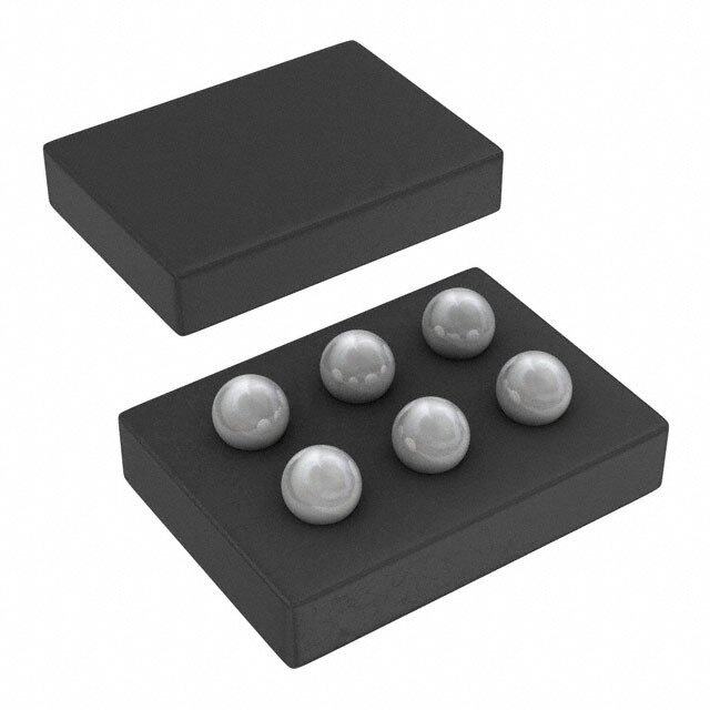
| 产品图片 |
|
| rohs | 符合RoHS无铅 / 符合限制有害物质指令(RoHS)规范要求 |
| 产品系列 | 板上安装温度传感器,Microchip Technology MCP9800A5T-M/OT- |
| 数据手册 | http://www.microchip.com/mymicrochip/filehandler.aspx?ddocname=en021183http://www.microchip.com/mymicrochip/filehandler.aspx?ddocname=en531282 |
| 产品型号 | MCP9800A5T-M/OT |
| 产品种类 | 板上安装温度传感器 |
| 传感器类型 | 内部 |
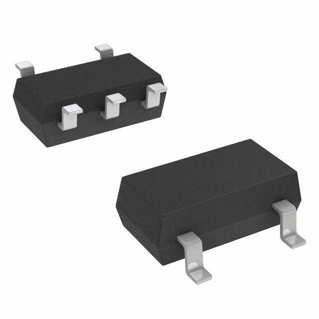
| 供应商器件封装 | SOT-23-5 |
| 关闭 | Shutdown |
| 其它名称 | MCP9800A5T-M/OTDKR |
| 准确性 | +/- 0.5 C |
| 功能 | 温度监控系统(传感器) |
| 包装 | Digi-Reel® |
| 参考设计库 | http://www.digikey.com/rdl/4294959886/4294959871/60 |
| 商标 | Microchip Technology |
| 安装类型 | 表面贴装 |
| 安装风格 | SMD/SMT |
| 封装 | Reel |
| 封装/外壳 | SC-74A,SOT-753 |
| 封装/箱体 | SOT-23A-5 |
| 工作温度 | -55°C ~ 125°C |
| 工厂包装数量 | 3000 |
| 感应温度 | -55°C ~ 125°C |
| 拓扑 | ADC(三角积分型),寄存器库 |
| 数字输出-位数 | 9 bit to 12 bit |
| 数字输出-总线接口 | 2-Wire, I2C, SMBus |
| 最大工作温度 | + 125 C |
| 最小工作温度 | - 55 C |
| 标准包装 | 1 |
| 温度阈值 | Programmable |
| 特色产品 | http://www.digikey.com/cn/zh/ph/Microchip/MCP9800.htmlhttp://www.digikey.com/product-highlights/cn/zh/microchip-mcp9800-family-temperature-sensors/3925 |
| 电压-电源 | 2.7 V ~ 5.5 V |
| 电源电压-最大 | 5.5 V |
| 电源电压-最小 | 2.7 V |
| 电源电流 | 200 uA |
| 精度 | ±2°C(最大) |
| 设备功能 | Sensor with Alert |
| 输出报警 | 无 |
| 输出电流 | 200 uA |
| 输出类型 | Digital |
| 输出风扇 | 是 |
| 配用 | /product-detail/zh/MCP9800DM-TS1/MCP9800DM-TS1-ND/1999546 |
| 配置 | Local |


- 商务部:美国ITC正式对集成电路等产品启动337调查
- 曝三星4nm工艺存在良率问题 高通将骁龙8 Gen1或转产台积电
- 太阳诱电将投资9.5亿元在常州建新厂生产MLCC 预计2023年完工
- 英特尔发布欧洲新工厂建设计划 深化IDM 2.0 战略
- 台积电先进制程称霸业界 有大客户加持明年业绩稳了
- 达到5530亿美元!SIA预计今年全球半导体销售额将创下新高
- 英特尔拟将自动驾驶子公司Mobileye上市 估值或超500亿美元
- 三星加码芯片和SET,合并消费电子和移动部门,撤换高东真等 CEO
- 三星电子宣布重大人事变动 还合并消费电子和移动部门
- 海关总署:前11个月进口集成电路产品价值2.52万亿元 增长14.8%


PDF Datasheet 数据手册内容提取
MCP9800/1/2/3 2-Wire High-Accuracy Temperature Sensor Features Description • Temperature-to-Digital Converter Microchip Technology Inc.’s MCP9800/1/2/3 family of (cid:127) Accuracy with 12-bit Resolution: digital temperature sensors converts temperatures between -55°C and +125°C to a digital word. They - ±0.5°C (typ.) at +25°C provide an accuracy of ±1°C (max.) from -10°C to - ±1°C (max.) from -10°C to +85°C +85°C. - ±2°C (max.) from -10°C to +125°C The MCP9800/1/2/3 family comes with user-program- - ±3°C (max.) from -55°C to +125°C mable registers that provide flexibility for temperature (cid:127) User-selectable Resolution: 9 – 12 bit sensing applications. The register settings allow user- (cid:127) Operating Voltage Range: 2.7V to 5.5V selectable 9-bit to 12-bit temperature measurement (cid:127) 2-wire Interface: I 2C™/SMBus Compatible resolution, configuration of the power-saving Shutdown (cid:127) Operating Current: 200µA (typ.) and One-shot (single conversion on command while in the Shutdown) modes and the specification of both (cid:127) Shutdown Current: 1µA (max.) temperature alert output and hysteresis limits. When (cid:127) Power-saving One-shot Temperature the temperature changes beyond the specified limits, Measurement the MCP9800/1/2/3 outputs an alert signal. The user (cid:127) Available Packages: SOT-23-5, MSOP-8, SOIC-8 has the option of setting the alert output signal polarity as an active-low or active-high comparator output for Typical Applications thermostat operation, or as temperature event interrupt output for microprocessor-based systems. (cid:127) Personal Computers and Servers This sensor has an industry standard 2-wire, I2C™/ (cid:127) Hard Disk Drives and Other PC Peripherals SMBus compatible serial interface, allowing up to eight (cid:127) Entertainment Systems devices to be controlled in a single serial bus. These fea- (cid:127) Office Equipment tures make the MCP9800/1/2/3 ideal for sophisticated (cid:127) Data Communication Equipment multi-zone temperature-monitoring applications. (cid:127) Mobile Phones Package Types (cid:127) General-purpose Temperature Monitoring Typical Application MCP9800 MCP9801 MCP9802 MCP9803 V SOT-23-5 SOIC, MSOP DD PICmicro® VDD 1 5 SDA SDA 1 8 VDD Microcontroller GND 2 SCLK 2 7 A0 MCP9800/02 R PIC16F737 ALERT 3 4 SCLK ALERT 3 6 A1 VDD 1 5 SDA IC2 GND 4 5 A2 GND 2 ™ ALERT 3 4 SCLK P MCP9800/02A0: A2, A1, A0 are internally set to (0, 0, 0) o I/O Port R rt MCP9800/02A5: A2, A1, A0 are internally set to (1, 0, 1) PULL-UP MCP9802/03: Serial Bus time-out 35ms (typ.) 2004 Microchip Technology Inc. DS21909B-page 1
MCP9800/1/2/3 1.0 ELECTRICAL PIN FUNCTION TABLE CHARACTERISTICS NAME FUNCTION Absolute Maximum Ratings † SDA Bidirectional Serial Data (open-drain output) VDD....................................................................... 6.0V SCLK Serial Clock Input Voltage at all Input/Output pins....GND – 0.3V to 5.5V ALERT Temperature Alert Output (open-drain) Storage temperature..........................-65°C to +150°C A2 Address Select Pin (bit 2) A1 Address Select Pin (bit 1) Ambient temp. with power applied.....-55°C to +125°C A0 Address Select Pin (bit 0) Junction Temperature (T )..................................150°C J V Power Supply Input DD ESD protection on all pins (HBM:MM).......(4kV:400V) GND Ground Latch-Up Current at each pin........................ ±200mA †Notice: Stresses above those listed under “Maximum ratings” may cause permanent damage to the device. This is a stress rating only and functional operation of the device at those or any other conditions above those indicated in the operational listings of this specification is not implied. Exposure to maximum rating conditions for extended periods may affect device reliability. DC CHARACTERISTICS Electrical Specifications: Unless otherwise indicated, V = 2.7V to 5.5V, GND = Ground, and DD T = -55°C to +125°C. A Parameters Sym Min Typ Max Unit Conditions Power Supply Operating Voltage Range V 2.7 — 5.5 V DD Operating Current I — 200 400 µA Continuous Operation DD Shutdown Current I — 0.1 1 µA Shutdown Mode SHDN Power On Reset Threshold (POR) V — 1.7 — V V falling edge POR DD Temperature Sensor Accuracy Accuracy with 12-bit Resolution: T = +25°C T — ±0.5 — °C V = 3.3V A ACY DD -10°C < T ≤ +85°C T -1.0 — +1.0 °C V = 3.3V A ACY DD -10°C < T ≤ +125°C T -2.0 — +2.0 °C V = 3.3V A ACY DD -55°C < T ≤ +125°C T -3.0 — +3.0 °C V = 3.3V A ACY DD Internal Σ∆ ADC Conversion Time: 9-bit Resolution t — 30 75 ms 33 samples/sec (typ.) CONV 10-bit Resolution t — 60 150 ms 17 samples/sec (typ.) CONV 11-bit Resolution t — 120 300 ms 8 samples/sec (typ.) CONV 12-bit Resolution t — 240 600 ms 4 samples/sec (typ.) CONV Alert Output (Open-drain) High-level Current I — — 1 µA V = 5V OH OH Low-level Voltage V — — 0.4 V I = 3mA OL OL Thermal Response Response Time t — 1.4 — s Time to 63% (88°C) RES 27°C (Air) to 125°C (oil bath) DS21909B-page 2 2004 Microchip Technology Inc.
MCP9800/1/2/3 DIGITAL INPUT/OUTPUT PIN CHARACTERISTICS Electrical Specifications: Unless otherwise indicated, V = 2.7V to 5.5V, GND = Ground and DD T = -55°C to +125°C. A Parameters Sym Min Typ Max Units Conditions Serial Input/Output (SCLK, SDA, A0, A1, A2) Input High-level Voltage V 0.7V — — V IH DD Low-level Voltage V — — 0.3V V IL DD Input Current I -1 — +1 µA IN Output (SDA) Low-level Voltage V — — 0.4 V I = 3mA OL OL High-level Current I — — 1 µA V = 5V OH OH Low-level Current I 6 — — mA V = 0.6V OL OL Capacitance C — 10 — pF IN SDA and SCLK Inputs Hysteresis V 0.05V — — V HYST DD Graphical Symbol Description INPUT OUTPUT Voltage Voltage V DD V DD V IH VIL VOL time time Current Current I OL I IN I OH time time TEMPERATURE CHARACTERISTICS Electrical Specifications: Unless otherwise indicated, V =+2.7V to +5.5V, GND = Ground. DD Parameters Sym Min Typ Max Units Conditions Temperature Ranges Specified Temperature Range T -55 — +125 °C (Note1) A Operating Temperature Range T -55 — +125 °C A Storage Temperature Range T -65 — +150 °C A Thermal Package Resistances Thermal Resistance, 5L-SOT23 θ — 256 — °C/W JA Thermal Resistance, 8L-SOIC θ — 163 — °C/W JA Thermal Resistance, 8L-MSOP θ — 206 — °C/W JA Note 1: Operation in this range must not cause T to exceed Maximum Junction Temperature (+150°C). J 2004 Microchip Technology Inc. DS21909B-page 3
MCP9800/1/2/3 SERIAL INTERFACE TIMING SPECIFICATIONS Electrical Specifications: Unless otherwise indicated, V = 2.7V to 5.5V, GND = Ground, -55°C < T < +125°C, DD A C = 80pF, and all limits measured to 50% point. L Parameters Sym Min Typ Max Units Conditions 2-Wire I2C/SMBus Compatible Interface Serial Port Frequency f 0 — 400 kHz I2C MCP9800/01 SC f 10 — 400 kHz SMBus MCP9802/03 SC Clock Period t 2.5 — — µs SC Low Clock t 1.3 — — µs LOW High Clock t 0.6 — — µs HIGH Rise Time t 20 — 300 ns 10% to 90% of V (SCLK, SDA) R DD Fall Time t 20 — 300 ns 90% to 10% of V (SCLK, SDA) F DD Data Setup Before SCLK High t 0.1 — — µs SU-DATA Data Hold After SCLK Low t 0 — 0.9 µs H-DATA Start Condition Setup Time t 0.6 — — µs SU-START Start Condition Hold Time t 0.6 — — µs H-START Stop Condition Setup Time t 0.6 — — µs SU-STOP Bus Idle t 1.3 — — µs IDLE Time Out t 25 35 50 ms MCP9802/03 only OUT Timing Diagram START Condition tSU-START tH-START SCLK SDA t Data Transmission OUT tHIGH tLOW SCLK SDA t ,t R F tSU-DATA tH-DATA tSC STOP Condition SCLK SDA t t SU-STOP IDLE DS21909B-page 4 2004 Microchip Technology Inc.
MCP9800/1/2/3 2.0 TYPICAL PERFORMANCE CURVES Note: Unless otherwise noted: V = 2.7V to 5.5V. DD 3.0 100% C) 12-Bit Resolution VDD= 3.3V 90% TA = +25°C 5 lots y (° 2.0 160 Samples 80% VDD = 3.3V 3126 0S Samamppleless/lot ature Accurac -011...000 Occurrences 3456700000%%%%% per 20% m -2.0 Te Spec. Limits 1 0 % -3.0 0% 0 5 0 5 0 5 0 5 0 5 0 5 0 -55 -35 -15 5 25 45 65 85 105 125 3. 2. 2. 1. 1. 0. 0. 0. 1. 1. 2. 2. 3. - - - - - - TA (°C) Temperature Accuracy (°C) FIGURE 2-1: Average Temperature FIGURE 2-4: Temperature Accuracy Accuracy vs. Ambient Temperature, V = 3.3V. Histogram, T = +25°C. DD A 3.0 400 C) 12-Bit Resolution e Accuracy (° 012...000 VVVVDDDDDDDD ==== 2355....7350VVVV 160 Samples (µA)D223305050000 VVVVDDDDDDDD ==== 2355....7350VVVV eratur -1.0 ID150 mp -2.0 100 e T -3.0 50 -55 -35 -15 5 25 45 65 85 105 125 -55 -35 -15 5 25 45 65 85 105 125 T (°C) T (°C) A A FIGURE 2-2: Average Temperature FIGURE 2-5: Supply Current vs. Ambient Accuracy vs. Ambient Temperature. Temperature. 3.0 1 C) Resolution VDD = 3.3V y (° 2.0 160 Samples 0.8 c cura 1.0 1112--BBiitt A) 0.6 c µ ature A -01..00 I (SHDN 0.4 mper -2.0 190--BBitit 0.2 e T -3.0 0 -55 -35 -15 5 25 45 65 85 105 125 -55 -35 -15 5 25 45 65 85 105 125 T (°C) T (°C ) A A FIGURE 2-3: Average Temperature FIGURE 2-6: Shutdown Current vs. Accuracy vs. Ambient Temperature, V = 3.3V. Ambient Temperature. DD 2004 Microchip Technology Inc. DS21909B-page 5
MCP9800/1/2/3 Note: Unless otherwise noted: V = 2.7V to 5.5V. DD 145 48 Average of 10 samples per package A) 42 VOL = 0.6V 125 m VDD = 5.5V C) RT & SDA I (OL 12338406 VVDDDD == 32..37VV mperature Data (° 146805555 MSSOOPIC E e AL 12 T 25 SOT-23 27°C (Air) to 125°C (Oil bath) 6 5 -55 -35 -15 5 25 45 65 85 105 125 -2 0 2 4 6 8 10 12 14 16 18 20 TA (°C) Time (s) FIGURE 2-7: ALERT and SDA I vs. FIGURE 2-9: MCP980X Thermal OL Ambient Temperature. Response vs Time. 0.4 IOL = 3mA V) (OL 0.3 SDA V 0.2 VVVDDDDDD === 532...537VVV & T ER 0.1 L A 0 -55 -35 -15 5 25 45 65 85 105 125 T (°C) A FIGURE 2-8: ALERT and SDA Output V vs. Ambient Temperature. OL DS21909B-page 6 2004 Microchip Technology Inc.
MCP9800/1/2/3 3.0 PIN DESCRIPTION The descriptions of the pins are listed in Table3-1. TABLE 3-1: PIN FUNCTION TABLE MCP9800 MCP9801 MCP9802 MCP9803 Symbol Function SOT-23-5 MSOP, SOIC 5 1 SDA Bidirectional Serial Data 4 2 SCLK Serial Clock Input 3 3 ALERT Temperature Alert Output 2 4 GND Ground — 5 A2 Address Select Pin (bit 2) — 6 A1 Address Select Pin (bit 1) — 7 A0 Address Select Pin (bit 0) 1 8 V Power Supply Input DD 3.1 Serial Data Pin (SDA) 3.5 ALERT Output The SDA is a bidirectional input/output pin, used to The MCP9800/1/2/3’s ALERT pin is an open-drain serially transmit data to and from the host controller. output pin. The device outputs an alert signal when the This pin requires a pull-up resistor to output data. ambient temperature goes beyond the user- programmed temperature limit. 3.2 Serial Clock Pin (SCLK) 3.6 Address Pins (A2, A1, A0) The SCLK is a clock input pin. All communication and timing is relative to the signal on this pin. The clock is These pins are device or slave address input pins and generated by the host controller on the bus. are available only with the MCP9801/03. The device addresses for the MCP9800/02 are factory-set. 3.3 Power Supply Input (V ) DD The address pins are the Least Significant bits (LSb) of the device address bits. The Most Significant bits The V pin is the power pin. The operating voltage, as DD (MSb) (A6, A5, A4, A3) are factory-set to <1001>. This specified in the DC electrical specification table, is is illustrated in Table3-2. applied on this pin. TABLE 3-2: SLAVE ADDRESS 3.4 Ground (GND) Device A6 A5 A4 A3 A2 A1 A0 The GND pin is the system ground pin. MCP9800/02A0 1 0 0 1 0 0 0 MCP9800/02A5 1 0 0 1 1 0 1 MCP9801/03 1 0 0 1 X X X Note: User-selectable address is shown by X. 2004 Microchip Technology Inc. DS21909B-page 7
MCP9800/1/2/3 4.0 FUNCTIONAL DESCRIPTION 4.1 Temperature Sensor The MCP9800/1/2/3 family of temperature sensors The MCP9800/1/2/3 uses the difference in the base- consists of a band-gap type temperature sensor, a Σ∆ emitter voltage of a transistor while its collector current Analog-to-Digital Converter (ADC), user-programmable is changed from IC1 to IC2. With this method, the ∆VBE registers and a 2-wire I2C/SMBus protocol compatible depends only on the ratio of the two currents and the serial interface. ambient temperature, as shown in Equation4-1. EQUATION 4-1: Resolution ∆V = k----T-- ×ln(IC ⁄IC ) BE q 1 2 One-Shot Shutdown Where: 9-Bit 10-Bit T = temperature in kelvin Fault Queue 11-Bit ∆V = change in diode base-emitter BE Alert Polarity 12-Bit voltage k = Boltzmann's constant Alert Comp/Int q = electron charge IC and IC = currents with n:1 ratio 1 2 Configuration Register Σ∆ ADC 4.2 Σ∆ Analog-to-Digital Converter Temperature Register A sigma-delta analog-to-digital converter is used to T convert ∆V to a digital word that corresponds to the HYST Band-Gap BE Register transistor temperature. The converter has an Temperature adjustable resolution from 9-bits (at 30ms conversion T Sensor SET time) to 12-bits (at 240ms conversion time). Thus, it Register allows the user to make trade-offs between resolution and conversion time. Refer to Section4.3.4 “Sensor Register I2C™/SMBus Configuration Register (CONFIG)” and Pointer Interface Section4.3.4.7 “Σ∆ ADC Resolution” for details. FIGURE 4-1: Functional Block Diagram. DS21909B-page 8 2004 Microchip Technology Inc.
MCP9800/1/2/3 4.3 Registers Resolution The MCP9800/1/2/3 family has four registers that are user-accessible. These registers are specified as the One-Shot ambient temperature register, the temperature limit-set register, the temperature hysteresis register and device Shutdown configuration registers. Fault Queue The ambient temperature register is a read-only register and is used to access the ambient temperature Alert Polarity data. The data from the ADC is loaded in parallel in the Alert Comp/Int register. The temperature limit-set and temperature hysteresis registers are read/write registers that Configuration provide user-programmable temperature limits. If the Register ambient temperature drifts beyond the programmed ALERT Temperature limits, the MCP9800/1/2/3 outputs an alert signal using Output Register the ALERT pin (refer to Section4.3.4.3 “ALERT Out- put Configuration”). The device configuration register T HYST ALERT Output provides access for the user to configure the Register Control Logic MCP9800/1/2/3’s various features. These registers are T described in further detail in the following sections. SET Register FIGURE 1: Register Block Diagram. The registers are accessed by sending register pointer to the MCP9800/1/2/3 using the serial interface. This is an 8-bit pointer. However, the two Least Significant bits (LSb) are used as pointers and all other bits need to be cleared <0>. This device has additional registers that are reserved for test and calibration. If these registers are accessed, the device may not perform according to the specification. The pointer description is shown below. REGISTER 4-1: REGISTER POINTER U-0 U-0 U-0 U-0 U-0 U-0 R/W-0 R/W-0 0 0 0 0 0 0 P1 P0 bit 7 bit 0 bit 7-3 Unimplemented: Read as ‘0’ bit 2-0 Pointer bits 00 = Temperature Register 01 = Configuration Register 10 = Temperature Hysteresis Register 11 = Temperature Limit-set Register Legend: R = Readable bit W = Writable bit U = Unimplemented bit, read as ‘0’ - n = Value at POR ‘1’ = Bit is set ‘0’ = Bit is cleared x = Bit is unknown 2004 Microchip Technology Inc. DS21909B-page 9
MCP9800/1/2/3 4.3.1 AMBIENT TEMPERATURE digital conversion in the background. The decimal code REGISTER (T ) to ambient temperature conversion is shown in A Equation4-2: The MCP9800/1/2/3 has a 16-bit read-only ambient temperature register (TA) that contains 9-bit to 12-bit EQUATION 4-2: temperature data. This data is formatted in two’s complement. The bit assignments, as well as the T = Code×2n A corresponding resolution, is shown in the register Where: assignment below. n = -1, -2, -3 and -4 for 9-bit, 10-bit, 11-bit The refresh rate of this register depends on the and 12-bit resolution, respectively selected ADC resolution. It takes 30ms (typ.) for 9-bit T = Ambient Temperature (°C) A data and 240ms (typ.) for 12-bit data. Since this Code= MCP980X output in decimal register is double-buffered, the user can read the (Table 4-1) register while the MCP9800/1/2/3 performs analog-to- REGISTER 4-2: AMBIENT TEMPERATURE REGISTER (T ) A Upper Half: R-0 R-0 R-0 R-0 R-0 R-0 R-0 R-0 Sign 26 °C/bit 25 °C/bit 24 °C/bit 23 °C/bit 22 °C/bit 21 °C/bit 20 °C/bit bit 15 bit 8 Lower Half: R-0 R-0 R-0 R-0 R-0 R-0 R-0 R-0 2-1 °C/bit 2-2 °C/bit 2-3 °C/bit 2-4 °C/bit 0 0 0 0 bit 7 bit 0 Note: When the 9-bit, 10-bit or 11-bit resolutions are selected, bit 6, bit 7 or bit 8 will remain clear <0>, respectively. Legend: R = Readable bit W = Writable bit U = Unimplemented bit, read as ‘0’ - n = Value at POR ‘1’ = Bit is set ‘0’ = Bit is cleared x = Bit is unknown TABLE 4-1: AMBIENT TEMPERATURE TO CODE CONVERSION Ambient Temperature Code T A 9-Bit 10-Bit 11-Bit 12-Bit Binary Hexadecimal Decimal (°C) +125°C 0111 1101 0uuu uuuu(1) 0FA 250 +125 +25.4375°C 0001 1001 0uuu uuuu 032 50 +25 +0.5°C 0000 0000 1uuu uuuu 001 1 +0.5 +125°C 0111 1101 00uu uuuu 1F4 500 +125 +25.4375°C 0001 1001 01uu uuuu 065 101 +25.25 +0.25°C 0000 0000 01uu uuuu 001 1 +0.25 +125°C 0111 1101 000u uuuu 3E8 1000 +125 +25.4375°C 0001 1001 011u uuuu 0CB 203 +25.375 +0.125°C 0000 0000 001u uuuu 001 1 +0.125 +125°C 0111 1101 0000 uuuu 7D0 2000 +125 +25.4375°C 0001 1001 0111 uuuu 197 407 +25.4375 +0.0625°C 0000 0000 0001 uuuu 001 1 +0.0625 0°C 0000 0000 0000 uuuu 000 0 0 –0.0625°C 1111 1111 1111 uuuu(2) 001(3) -1 -0.0625 –25.4375°C 1110 0110 1001 uuuu 197 -407 -25.4375 –55°C 1100 1001 0000 uuuu 370 -880 -55 Note 1: ‘u’ represents unused bits. The MCP9800/1/2/3 clears <0> the unused bits. 2: This data is in two’s complement format, which indicates ambient temperature below 0°C. 3: Negative temperature magnitude in Hexadecimal. This conversion is done by complimenting each binary bit and adding 1. DS21909B-page 10 2004 Microchip Technology Inc.
MCP9800/1/2/3 4.3.2 TEMPERATURE LIMIT-SET REGISTER (T ) SET The MCP9800/1/2/3 has a 16-bit read/write Tempera- ture Limit-Set register (T ) which contains a 9-bit data SET in two’s compliment format. This data represents a maximum temperature limit. If the ambient temperature exceeds this specified limit, the MCP9800/1/2/3 asserts an alert output. (Refer to Section4.3.4.3 “ALERT Out- put Configuration”). This register uses the nine Most Significant bits (MSb) and all other bits are don’t cares. The power-up default value of T register is 80°C SET <0 1010 0000> in binary. REGISTER 4-3: TEMPERATURE LIMIT-SET REGIST ER (T ) SET Upper Half: R/W-0 R/W-0 R/W-0 R/W-0 R/W-0 R/W-0 R/W-0 R/W-0 Sign 26 °C/bit 25 °C/bit 24 °C/bit 23 °C/bit 22 °C/bit 21 °C/bit 20 °C/bit bit 15 bit 8 Lower Half: R/W-0 R-0 R-0 R-0 R-0 R-0 R-0 R-0 2-1 °C/bit 0 0 0 0 0 0 0 bit 7 bit 0 Legend: R = Readable bit W = Writable bit U = Unimplemented bit, read as ‘0’ - n = Value at POR ‘1’ = Bit is set ‘0’ = Bit is cleared x = Bit is unknown 2004 Microchip Technology Inc. DS21909B-page 11
MCP9800/1/2/3 4.3.3 TEMPERATURE HYSTERESIS REGISTER (T ) HYST The MCP9800/1/2/3 has a 16-bit read/write tempera- ture hysteresis register (T ) that contains a 9-bit HYST data in two’s compliment format. This register is used to set a hysteresis for the T limit. Therefore, the data SET represents a minimum temperature limit. If the ambient temperature drifts below the specified limit, the MCP9800/1/2/3 asserts an alert output (refer to Section4.3.4.3 “ALERT Output Configuration”). This register uses the nine Most Significant bits (MSb) and all other bits are don’t cares. The power-up default value of T register is 75°C HYST <0 1001 0110> in binary. R EGISTER 4-4: TEMPERATURE HYSTERESIS REGISTER (T ) HYST Upper Half: R/W-0 R/W-0 R/W-0 R/W-0 R/W-0 R/W-0 R/W-0 R/W-0 Sign 26 °C/bit 25 °C/bit 24 °C/bit 23 °C/bit 22 °C/bit 21 °C/bit 20 °C/bit bit 15 bit 8 Lower Half: R/W-0 R-0 R-0 R-0 R-0 R-0 R-0 R-0 2-1 °C/bit 0 0 0 0 0 0 0 bit 7 bit 0 Legend: R = Readable bit W = Writable bit U = Unimplemented bit, read as ‘0’ - n = Value at POR ‘1’ = Bit is set ‘0’ = Bit is cleared x = Bit is unknown DS21909B-page 12 2004 Microchip Technology Inc.
MCP9800/1/2/3 4.3.4 SENSOR CONFIGURATION REGISTER (CONFIG) The MCP9800/1/2/3 has an 8-bit read/write configura- tion register (CONFIG) that allows the user to select the different features. These features include shutdown, ALERT output select as comparator or interrupt output, ALERT output polarity, fault queue cycle, temperature measurement resolution and One-shot mode (single conversion while in shutdown). These functions are described in detail in the following sections. REGISTER 4-5: CONFIGURATION REGISTER (CONFIG) R/W-0 R/W-0 R/W-0 R/W-0 R/W-0 R/W-0 R/W-0 R/W-0 One-Shot Resolution Fault Queue ALERT COMP/ Shut- Polarity INT down bit 7 bit 0 bit 7 ONE-SHOT bit 1 = Enabled 0 = Disabled (Power-up default) bit 5-6 Σ∆ ADC RESOLUTION bit 00 = 9 bit (Power-up default) 01 = 10 bit 10 = 11 bit 11 = 12 bit bit 3-4 FAULT QUEUE bit 00 = 1 (Power-up default) 01 = 2 10 = 4 11 = 6 bit 2 ALERT POLARITY bit 1 = Active-High 0 = Active-Low (Power-up default) bit 1 COMP/INT bit 1 = Interrupt Mode 0 = Comparator Mode (Power-up default) bit 0 SHUTDOWN bit 1 = Enable 0 = Disable (Power-up default) Legend: R = Readable bit W = Writable bit U = Unimplemented bit, read as ‘0’ - n = Value at POR ‘1’ = Bit is set ‘0’ = Bit is cleared x = Bit is unknown 2004 Microchip Technology Inc. DS21909B-page 13
MCP9800/1/2/3 4.3.4.1 Shutdown Mode 4.3.4.3 ALERT Output Configuration The Shutdown mode disables all power-consuming The ALERT output can be configured as either a activities (including temperature sampling operations) comparator output or as Interrupt Output mode using while leaving the serial interface active. The device bit 1 of CONFIG. The polarity can also be specified as consumes 1µA (max.) in this mode. It remains in this an active-high or active-low, using bit 2 of CONFIG. mode until the configuration register is updated to The following sections describe each Output mode enable continuous conversion or until power is and Figure4-2 shows graphical description. recycled. 4.3.4.4 Comparator Mode In Shutdown mode, the CONFIG, T , T and T A SET HYST registers can be read or written. However, the serial In the Comparator mode, the ALERT output is asserted bus activity will increase the shutdown current. when TA is greater than TSET. The pin remains active until T is lower than T . The Comparator mode is A HYST 4.3.4.2 One-Shot Mode useful for thermostat-type applications such as turning on a cooling fan or triggering a system shutdown when The MCP9800/1/2/3 can also be used in a One-shot the temperature exceeds a safe operating range. mode that can be selected using bit 7 of the CONFIG register. The One-shot mode performs a single temper- In the Comparator mode, if the device enters the ature measurement and returns to Shutdown mode. Shutdown mode with asserted ALERT output, the This mode is especially useful for low-power applica- output remains active during shutdown. The device tions where temperature is measured upon command must be operating in continuous conversion, with T A from a controller. For example, a 9-bit T in One-shot below T , for the ALERT output to be deasserted. A HYST mode consumes 200µA (typ.) for 30ms and 0.1µA (typ.) during shutdown. 4.3.4.5 Interrupt Mode To access this feature, the device needs to initially be In the Interrupt mode, the ALERT output is asserted in Shutdown mode. This is done by sending a byte to when TA is greater than TSET. However, the output is the CONFIG register with bit 0 set <1> and bit 7 deasserted when the user performs a read from any cleared <0>. Once the device is in Shutdown mode, register. This mode is designed for interrupt driven micro- CONFIG needs to be written again with bit 0 and bit 7 controller based systems. The microcontroller receiving set <1>. This begins the single conversion cycle of the interrupt will have to acknowledge the interrupt by 30ms for 9-bit data. Once the conversion is reading any register from the MCP9800/1/2/3. This will completed, T is updated and bit 7 of CONFIG clear the interrupt and the ALERT pin will become A becomes cleared <0> by the MCP9800/1/2/3. deasserted. When TA drifts below THYST, the MCP9800/ 1/2/3 outputs another interrupt and the controller needs TABLE 4-6: SHUTDOWN AND ONE-SHOT to read a register to deassert the ALERT output. Shutting MODE DESCRIPTION down the device will also reset or deassert the ALERT One-Shot Shutdown output. Operational Mode (Bit 7) (Bit 0) Continuous Conversion 0 0 T Shutdown 0 1 SET T Continuous Conversion 1 0 A (One-shot is ignored) T HYST One-Shot 1 1 Note: The shutdown command <01> needs to be programmed before sending a one- ALERT shot command <11>. Comparator Mode Active-Low ALERT Interrupt Mode Active-Low FIGURE 4-2: Alert Output. DS21909B-page 14 2004 Microchip Technology Inc.
MCP9800/1/2/3 4.3.4.6 Fault Queue 4.4 Summary of Power-up Default The fault queue feature can be used as a filter to lessen The MCP9800/1/2/3 has an internal Power-on Reset the probability of spurious activation of the ALERT pin. (POR) circuit. If the power supply voltage V glitches DD TA must remain above TSET for the consecutive num- down to the 1.7V (typ.) threshold, the device resets the ber of conversion cycles selected using the Fault registers to the power-up default settings. Queue bits. Bit 3 and bit 4 of CONFIG can be used to Table4-2 shows the power-up default summary. select up to six fault queue cycles. For example, if six fault queues are selected, T must be greater than A TABLE 4-2: POWER-UP DEFAULTS T for six consecutive conversions before ALERT is SET asserted as a comparator or an interrupt output. Data Register Power-up Defaults This queue setting also applies for T . T must (Hex) HYST A remain below THYST for six consecutive conversions TA 0000 0°C before ALERT is deasserted (comparator mode) or T A000 80°C SET before another interrupt is asserted (interrupt mode). T 9600 75°C HYST 4.3.4.7 Σ∆ ADC Resolution Pointer 00 Temperature register Continuous Conversion The MCP9800/1/2/3 provides access to select the ADC Comparator mode resolution from 9-bit to 12-bit using bit 6 and bit 5 of the CONFIG 00 Active-Low Output CONFIG register. The user can gain better insight into Fault Queue 1 the trends and characteristics of the ambient 9-bit Resolution temperature by using a finer resolution. Increasing the resolution also reduces the quantization error. Figure2-4 shows accuracy versus resolution. Table4-1 shows the T register conversion time for the A corresponding resolution. TABLE 4-1: RESOLUTION AND CONVERSION TIME Resolution Conversion time Bits °C/Bit (typ.) t ms (typ.) CONV 9 0.5 30 10 0.25 60 11 0.125 120 12 0.0625 240 2004 Microchip Technology Inc. DS21909B-page 15
MCP9800/1/2/3 5.0 SERIAL COMMUNICATION 5.1.2 MASTER/SLAVE The bus is controlled by a master device (typically a 5.1 2-Wire I2C/SMBus Compatible microcontroller) that controls the bus access and gener- Interface ates the start and stop conditions. The MCP9800/1/2/3 is a slave device and does not control other devices in The MCP9800/1/2/3 serial clock input (SCLK) and the the bus. Both master and slave devices can operate as bidirectional serial data line (SDA) form a 2-Wire either transmitter or receiver. However, the master bidirectional serial port for communication. device determines which mode is activated. The following bus protocol has been defined: 5.1.3 START/STOP CONDITION TABLE 5-1: MCP980X SERIAL BUS A high-to-low transition of the SDA line (while SCLK is CONVENTIONS high) is the start condition. All data transfers must be Term Description preceded by a start condition from the master. If a start condition is generated during data transfer, the Transmitter Device sending data to the bus MCP9800/1/2/3 resets and accepts the new start Receiver Device receiving data from the bus condition. Master The device that controls the serial bus, A low-to-high transition of the SDA line (while SCLK is typically a microcontroller high) is the stop condition. All data transfers must be Slave The device addressed by the master, ended by a stop condition from the master. If a stop such as the MCP9800/1/2/3 condition is introduced during data transmission, the MCP9800/1/2/3 releases the bus. START A unique signal from master to initiate serial interface with a slave 5.1.4 ADDRESS BYTE STOP A unique signal from the master to Following the start condition, the host must transmit the terminate serial interface from a slave address byte to the MCP9800/1/2/3. The 7-bit address Read/Write A read or write to the MCP9800/1/2/3 for the MCP9800/02A0 and MCP9800/02A5 is registers <1001000> and <1001101> in binary, respectively. ACK A receiver Acknowledges (ACK) the The address for the MCP9802/03 is reception of each byte by polling the <1001,A2,A1,A0> in binary, where the A0, A1 and A2 bus bits are set externally by connecting the corresponding NAK A receiver Not-Acknowledges (NAK) or pins to VDD <1> or GND <0>. The 7-bit address trans- mitted in the serial bit stream must match the selected releases the bus to show End-of-Data (EOD) address for the MCP9800/1/2/3 to respond with an ACK. Busy Communication is not possible because the bus is in use Bit 8 in the address byte is a read/write bit. Setting this bit to ‘1’ commands a read operation, while ‘0’ Not Busy The bus is in the idle state, both SDA commands a write operation. and SCLK remain high Data Valid SDA must remain stable before SCLK Address Byte becomes high in order for a data bit to be considered valid. During normal data transfers, SDA only changes state SCLK 1 2 3 4 5 6 7 8 9 while SCLK is low A C 5.1.1 DATA TRANSFER SDA 1 0 0 1 A2 A1 A0 K Start Data transfers are initiated by a start condition Address Slave (START), followed by a 7-bit device address and a 1-bit Code Address R/W read/write. Acknowledge (ACK) from slave confirms MCP9800/1/2/3 Response the reception of each byte. Each access must be terminated by a stop condition (STOP). FIGURE 5-1: Device Addressing. Data transfer may be initiated when the bus is in IDLE. DS21909B-page 16 2004 Microchip Technology Inc.
MCP9800/1/2/3 5.1.5 DATA VALID 5.1.7 TIME OUT (MCP9802/03) After the start condition, each bit of data in transmission If the SCLK stays low for time specified by t , the OUT needs to be settled for time specified by t MCP9802/03 resets the serial interface. This dictates SU-DATA before SCLK toggles from low-to-high (refer to the the minimum clock speed as specified in the SMBus Serial Interface Timing Specification). specification. The I2C bus specification does not limit clock speed and, therefore, the master can hold the 5.1.6 ACKNOWLEDGE (ACK) clock indefinitely to process data (MCP9800/01 only). Each receiving device, when addressed, is obliged to generate an acknowledge bit after the reception of each byte. The master device must generate an extra clock pulse for ACK to be recognized. The acknowledging device has to pull down the SDA line for t before the low-to-high transition of SU-DATA SCLK from the Master and remains pulled down for t after high-to-low transition of SCLK. H-DATA During read, the master must signal an End-of-Data (EOD) to the slave by not generating an ACK bit once the last bit has been clocked out of the slave. In this case, the slave will leave the data line released to enable the master to generate the stop condition. 2004 Microchip Technology Inc. DS21909B-page 17
MCP9800/1/2/3 5.2 Graphical Representation of the MCP9800/1/2/3 Serial Protocols Read 1-byte Data 1 2 3 4 5 6 7 8 1 2 3 4 5 6 7 8 SCLK A A SDA S 1 0 0 1 A A A W C 0 0 0 0 0 0 P P C 2 1 0 K 1 0 K Address Byte Pointer MCP980X MCP980X 1 2 3 4 5 6 7 8 1 2 3 4 5 6 7 8 SCLK SDA S 1 0 0 1 A A A R AC D D D D D D D D NA P 2 1 0 K 7 6 5 4 3 2 1 0 K Address Byte Data MCP980X Master Read 2-byte Data 1 2 3 4 5 6 7 8 1 2 3 4 5 6 7 8 SCLK A A SDA S 1 0 0 1 A A A W C 0 0 0 0 0 0 P P C 2 1 0 K 1 0 K Address Byte Pointer MCP980X MCP980X 1 2 3 4 5 6 7 8 1 2 3 4 5 6 7 8 1 2 3 4 5 6 7 8 SCLK SDA S 1 0 0 1 A A A R AC D D D D D D D D AC D D D D D D D D NA P 2 1 0 K 15 14 13 12 11 10 9 8 K 7 6 5 4 3 2 1 0 K Address Byte MSB Data LSB Data Master MCP980X Master S = START Condition P = STOP Condition FIGURE 5-2: Read 1-byteand 2-byte data from a Register. DS21909B-page 18 2004 Microchip Technology Inc.
MCP9800/1/2/3 Write 1-byte Data 1 2 3 4 5 6 7 8 1 2 3 4 5 6 7 8 1 2 3 4 5 6 7 8 SCLK SDA S 1 0 0 1 A A A W AC 0 0 0 0 0 0 P P AC D D D D D D D D AC P 2 1 0 K 1 0 K 7 6 5 4 3 2 1 0 K Address Byte Pointer Data MCP980X MCP980X MCP980X Write 2-byte Data 1 2 3 4 5 6 7 8 1 2 3 4 5 6 7 8 SCLK A A SDA S 1 0 0 1 A A A W C 0 0 0 0 0 0 P P C 2 1 0 K 1 0 K Address Byte Pointer MCP980X MCP980X 1 2 3 4 5 6 7 8 1 2 3 4 5 6 7 8 D D D D D D D D AC D D D D D D D D AC P 15 14 13 12 11 10 9 8 K 7 6 5 4 3 2 1 0 K MSB Data LSB Data S = START Condition MCP980X MCP980X P = STOP Condition FIGURE 5-3: Write 1-byte and 2-byte data from a Register. 2004 Microchip Technology Inc. DS21909B-page 19
MCP9800/1/2/3 Register Pointer Setting for Continuous Reception 1 2 3 4 5 6 7 8 1 2 3 4 5 6 7 8 SCLK A A SDA S 1 0 0 1 A A A W C 0 0 0 0 0 0 P P C 2 1 0 K 1 0 K Address Byte Pointer MCP980X MCP980X Receive 1-byte Data 1 2 3 4 5 6 7 8 1 2 3 4 5 6 7 8 SCLK SDA S 1 0 0 1 A A A R AC D D D D D D D D NA P 2 1 0 K 7 6 5 4 3 2 1 0 K Address Byte Data MCP980X Master Receive Another 1-byte Data 1 2 3 4 5 6 7 8 1 2 3 4 5 6 7 8 SCLK SDA S 1 0 0 1 A A A R AC D D D D D D D D NA P 2 1 0 K 7 6 5 4 3 2 1 0 K Address Byte Data MCP980X Master Note: User can continue to receive 1-byte data indefinitely from a previously set register pointer. S = START Condition P = STOP Condition FIGURE 5-4: Receive 1-byte data from previously set pointer. DS21909B-page 20 2004 Microchip Technology Inc.
MCP9800/1/2/3 Register Pointer Setting for Continuous Reception 1 2 3 4 5 6 7 8 1 2 3 4 5 6 7 8 SCLK A A SDA S 1 0 0 1 A A A W C 0 0 0 0 0 0 P P C 2 1 0 K 1 0 K Address Byte Pointer MCP980X MCP980X Receive 2-byte Data 1 2 3 4 5 6 7 8 1 2 3 4 5 6 7 8 1 2 3 4 5 6 7 8 S 1 0 0 1 A A A R AC D D D D D D D D AC D D D D D D D D NA P 2 1 0 K 15 14 13 12 11 10 9 8 K 7 6 5 4 3 2 1 0 K Address Byte MSB Data LSB Data Master MCP980X Master Receive Another 2-byte Data 1 2 3 4 5 6 7 8 1 2 3 4 5 6 7 8 1 2 3 4 5 6 7 8 S 1 0 0 1 A A A R AC D D D D D D D D AC D D D D D D D D NA P 2 1 0 K 15 14 13 12 11 10 9 8 K 7 6 5 4 3 2 1 0 K Address Byte MSB Data LSB Data Master MCP980X Master Note: User can continue to receive 2-byte data indefinitely from a previously set register pointer. S = START Condition P = STOP Condition FIGURE 5-5: Receive 2-byte data from previously set pointer. 2004 Microchip Technology Inc. DS21909B-page 21
MCP9800/1/2/3 6.0 APPLICATIONS INFORMATION SDA SCLK 6.1 Connecting to the Serial Bus PIC16F737 Microcontroller The SDA and SCLK serial interface are open-drain pins that require pull-up resistors. This configuration is 24LC01 shown in Figure6-1. EEPROM TC654 V Fan Speed DD Controller MCP980X Temperature er MCP980X Sensor ®ooll R R crntr SDA mio c SCLK FIGURE 6-2: Multiple Devices on SMBus. Co PIcr Mi The ALERT output can be wire-ORed with a number of other open-drain devices. In such applications, the output needs to be programmed as an active-low FIGURE 6-1: Pull-up Resistors On Serial output. Most systems will require pull-up resistors for Interface. this configuration. For the SMBus protocol, the number of devices con- 6.3 Layout Considerations nected to the bus are limited only by the maximum rise and fall times of the SDA and SCLK lines. Unlike the The MCP9800/1/2/3 does not require any additional I2C specifications, SMBus does not specify a maximum components besides the Master controller in order to bus capacitance value. Rather, it specifies 350µA measure temperature. However, it is recommended (max.) current through the pull-up resistor. Therefore, that a decoupling capacitor of 0.1µF to 1µF be used the value of the pull-up resistors will vary depending on between the V and GND pins. A high-frequency the system’s supply voltage (V ). The pull-up resistor DD DD ceramic capacitor is recommended. It is necessary for values for a 5V system ranges 14.3kΩ to 50kΩ. the capacitor to be located as close as possible to the Minimizing bus capacitance is still very important, as it power pins in order to provide effective noise directly affects the rise and fall times of the SDA and protection. SCLK lines. Although SMBus specifications only require the SDA 6.4 Thermal Considerations and SCLK lines to pull down 350µA (max.) with 0.4V The MCP9800/1/2/3 measures temperature by (max.) voltage drop, the MCP9800/1/2/3 is designed to monitoring the voltage of a diode located in the die. A meet 0.4V (max.) voltage drop at 3mA of current. This low impedance thermal path between the die and the allows the MCP9800/1/2/3 to drive lower values of pull- Printed Circuit Board (PCB) is provided by the pins. up resistors and higher bus capacitance. In this Therefore, the MCP9800/1/2/3 effectively monitors the application, all devices on the bus must meet the same temperature of the PCB. However, the thermal path for pull-down current requirements. the ambient air is not as efficient because the plastic device package functions as a thermal insulator. 6.2 Typical Application A potential for self-heating errors can exist if the Microchip provides several microcontroller product MCP9800/1/2/3 SDA and SCLK communication lines lines with Master Synchronous Serial Port Modules are heavily loaded with pull-ups. Typically, the self- (MSSP) that include I2C interface mode. This module heating error is negligible because of the relatively implements all master and slave functions and simpli- small current consumption of the MCP9800/1/2/3. fies the firmware development overhead. Figure6-2 However, in order to maximize the temperature shows a typical application using the PIC16F737 as a accuracy, the SDA and SCLK pins need to be lightly master to control other Microchip slave products, such loaded. as EEPROM, fan speed controllers and the MCP980X temperature sensor connected to the bus. DS21909B-page 22 2004 Microchip Technology Inc.
MCP9800/1/2/3 7.0 PACKAGING INFORMATION 7.1 Package Marking Information 5-Lead SOT-23 Example: XXNN Part Number MCP9800 Part Number MCP9802 MCP9800A0T-M/OTG LDNN MCP9802A0T-M/OTG JKNN MCP9800A5T-M/OTG LJNN MCP9802A5T-M/OTG JRNN 8-Lead MSOP Example: XXXXX G9803M YWWNNN 425256 8-Lead SOIC (150 mil) Example: XXXXXXXX GMCP9803 XXXXYYWW M/SN0425 NNN 256 Legend: XX...X Customer specific information* YY Year code (last 2 digits of calendar year) WW Week code (week of January 1 is week ‘01’) NNN Alphanumeric traceability code Note: In the event the full Microchip part number cannot be marked on one line, it will be carried over to the next line thus limiting the number of available characters for customer specific information. * Standard OTP marking consists of Microchip part number, year code, week code, and traceability code. 2004 Microchip Technology Inc. DS21909B-page 23
MCP9800/1/2/3 5-Lead Plastic Small Outline Transistor (OT) (SOT-23) E E1 p B p1 D n 1 α c A A2 φ A1 L β Units INCHES* MILLIMETERS Dimension Limits MIN NOM MAX MIN NOM MAX Number of Pins n 5 5 Pitch p .038 0.95 Outside lead pitch (basic) p1 .075 1.90 Overall Height A .035 .046 .057 0.90 1.18 1.45 Molded Package Thickness A2 .035 .043 .051 0.90 1.10 1.30 Standoff A1 .000 .003 .006 0.00 0.08 0.15 Overall Width E .102 .110 .118 2.60 2.80 3.00 Molded Package Width E1 .059 .064 .069 1.50 1.63 1.75 Overall Length D .110 .116 .122 2.80 2.95 3.10 Foot Length L .014 .018 .022 0.35 0.45 0.55 Foot Angle φ 0 5 10 0 5 10 Lead Thickness c .004 .006 .008 0.09 0.15 0.20 Lead Width B .014 .017 .020 0.35 0.43 0.50 Mold Draft Angle Top α 0 5 10 0 5 10 Mold Draft Angle Bottom β 0 5 10 0 5 10 *Controlling Parameter Notes: Dimensions D and E1 do not include mold flash or protrusions. Mold flash or protrusions shall not exceed .005" (0.127mm) per side. EIAJ Equivalent: SC-74A Drawing No. C04-091 DS21909B-page 24 2004 Microchip Technology Inc.
MCP9800/1/2/3 8-Lead Plastic Micro Small Outline Package (MS) (MSOP) E E1 p D 2 B n 1 α A A2 c φ A1 (F) L β Units INCHES MILLIMETERS* Dimension Limits MIN NOM MAX MIN NOM MAX Number of Pins n 8 8 Pitch p .026 BSC 0.65 BSC Overall Height A - - .043 - - 1.10 Molded Package Thickness A2 .030 .033 .037 0.75 0.85 0.95 Standoff A1 .000 - .006 0.00 - 0.15 Overall Width E .193 TYP. 4.90 BSC Molded Package Width E1 .118 BSC 3.00 BSC Overall Length D .118 BSC 3.00 BSC Foot Length L .016 .024 .031 0.40 0.60 0.80 Footprint (Reference) F .037 REF 0.95 REF Foot Angle φ 0° - 8° 0° - 8° Lead Thickness c .003 .006 .009 0.08 - 0.23 Lead Width B .009 .012 .016 0.22 - 0.40 Mold Draft Angle Top α 5° - 15° 5° - 15° Mold Draft Angle Bottom β 5° - 15° 5° - 15° *Controlling Parameter Notes: Dimensions D and E1 do not include mold flash or protrusions. Mold flash or protrusions shall not exceed .010" (0.254mm) per side. JEDEC Equivalent: MO-187 Drawing No. C04-111 2004 Microchip Technology Inc. DS21909B-page 25
MCP9800/1/2/3 8-Lead Plastic Small Outline (SN) – Narrow, 150 mil Body (SOIC) E E1 p D 2 B n 1 h α 45° c A A2 φ β L A1 Units INCHES* MILLIMETERS Dimension Limits MIN NOM MAX MIN NOM MAX Number of Pins n 8 8 Pitch p .050 1.27 Overall Height A .053 .061 .069 1.35 1.55 1.75 Molded Package Thickness A2 .052 .056 .061 1.32 1.42 1.55 Standoff § A1 .004 .007 .010 0.10 0.18 0.25 Overall Width E .228 .237 .244 5.79 6.02 6.20 Molded Package Width E1 .146 .154 .157 3.71 3.91 3.99 Overall Length D .189 .193 .197 4.80 4.90 5.00 Chamfer Distance h .010 .015 .020 0.25 0.38 0.51 Foot Length L .019 .025 .030 0.48 0.62 0.76 Foot Angle φ 0 4 8 0 4 8 Lead Thickness c .008 .009 .010 0.20 0.23 0.25 Lead Width B .013 .017 .020 0.33 0.42 0.51 Mold Draft Angle Top α 0 12 15 0 12 15 Mold Draft Angle Bottom β 0 12 15 0 12 15 * Controlling Parameter § Significant Characteristic Notes: Dimensions D and E1 do not include mold flash or protrusions. Mold flash or protrusions shall not exceed .010” (0.254mm) per side. JEDEC Equivalent: MS-012 Drawing No. C04-057 DS21909B-page 26 2004 Microchip Technology Inc.
MCP9800/1/2/3 PRODUCT IDENTIFICATION SYSTEM To order or obtain information, e.g., on pricing or delivery, refer to the factory or the listed sales office. PART NO. XX X –X /XX X Examples: a) MCP9800A0T-M/OTG Slave address ‘000’, Device Slave Tape & Reel Temperature Package PB Free Tape and Reel, Address Range -55°C to +125°C, PB Free SOT-23 package. b) MCP9800A5T-M/OTG Slave address ‘101’, Tape and Reel, Device: MCP9800: Temperature Sensor -55°C to +125°C, PB MCP9801: Temperature Sensor Free SOT-23 package. MCP9802: Temperature Sensor MCP9803: Temperature Sensor a) MCP9801-M/MSG -55°C to +125°C, PB Free 8LD MSOP package. A0 = Slave address set to ‘000’ b) MCP9801T-M/MSG Tape and Reel, -55°C A5 = Slave address set to ‘101’ to +125°C, PB Free 8LD MSOP package. c) MCP9801-M/SNG -55°C to +125°C, PB Tape and Reel: = Blank Free 8LD SOIC T = Tape and Reel package. d) MCP9801T-M/SNG Tape and Reel, -55°C to +125°C, PB Free Temperature M = -55°C to +125°C 8LD SOIC package. Range: a) MCP9802A0T-M/OT Slave address ‘000’, Tape and Reel, -55°C Package: OT = Plastic Small Outline Transistor (SOT-23), 5-lead to +125°C, SOT-23 MS = Plastic Micro Small Outline (MSOP), 8-lead package. SN = Plastic SOIC, (150 mil Body), 8-lead b) MCP9802A5T-M/OT Slave address ‘101’, Tape and Reel, -55°C to +125°C, SOT-23 PB Free: G = Lead Free device package. a) MCP9803-M/MSG -55°C to +125°C, PB Free 8LD MSOP package. b) MCP9803T-M/MSG Tape and Reel, -55°C to +125°C, PB Free 8LD MSOP package. c) MCP9803-M/SNG -55°C to +125°C, PB Free 8LD SOIC package. d) MCP9803T-M/SNG Tape and Reel, -55°C to +125°C, PB Free 8LD SOIC package. Sales and Support Data Sheets Products supported by a preliminary Data Sheet may have an errata sheet describing minor operational differences and recommended workarounds. To determine if an errata sheet exists for a particular device, please contact one of the following: 1. Your local Microchip sales office 2. The Microchip Corporate Literature Center U.S. FAX: (480) 792-7277 3. The Microchip Worldwide Site (www.microchip.com) Please specify which device, revision of silicon and Data Sheet (include Literature #) you are using. New Customer Notification System Register on our web site (www.microchip.com) to receive the most current information on our products. 2004 Microchip Technology Inc. DS21909B-page 27
MCP9800/1/2/3 NOTES: DS21909B-page 28 2004 Microchip Technology Inc.
Note the following details of the code protection feature on Microchip devices: (cid:127) Microchip products meet the specification contained in their particular Microchip Data Sheet. (cid:127) Microchip believes that its family of products is one of the most secure families of its kind on the market today, when used in the intended manner and under normal conditions. (cid:127) There are dishonest and possibly illegal methods used to breach the code protection feature. All of these methods, to our knowledge, require using the Microchip products in a manner outside the operating specifications contained in Microchip’s Data Sheets. Most likely, the person doing so is engaged in theft of intellectual property. (cid:127) Microchip is willing to work with the customer who is concerned about the integrity of their code. (cid:127) Neither Microchip nor any other semiconductor manufacturer can guarantee the security of their code. Code protection does not mean that we are guaranteeing the product as “unbreakable.” Code protection is constantly evolving. We at Microchip are committed to continuously improving the code protection features of our products. Attempts to break Microchip’s code protection feature may be a violation of the Digital Millennium Copyright Act. If such acts allow unauthorized access to your software or other copyrighted work, you may have a right to sue for relief under that Act. Information contained in this publication regarding device Trademarks applications and the like is provided only for your convenience The Microchip name and logo, the Microchip logo, Accuron, and may be superseded by updates. It is your responsibility to dsPIC, KEELOQ, microID, MPLAB, PIC, PICmicro, ensure that your application meets with your specifications. PICSTART, PROMATE, PowerSmart, rfPIC, and MICROCHIP MAKES NO REPRESENTATIONS OR WAR- SmartShunt are registered trademarks of Microchip RANTIES OF ANY KIND WHETHER EXPRESS OR IMPLIED, Technology Incorporated in the U.S.A. and other countries. WRITTEN OR ORAL, STATUTORY OR OTHERWISE, RELATED TO THE INFORMATION, INCLUDING BUT NOT AmpLab, FilterLab, MXDEV, MXLAB, PICMASTER, SEEVAL, LIMITED TO ITS CONDITION, QUALITY, PERFORMANCE, SmartSensor and The Embedded Control Solutions Company MERCHANTABILITY OR FITNESS FOR PURPOSE. are registered trademarks of Microchip Technology Microchip disclaims all liability arising from this information and Incorporated in the U.S.A. its use. Use of Microchip’s products as critical components in Analog-for-the-Digital Age, Application Maestro, dsPICDEM, life support systems is not authorized except with express dsPICDEM.net, dsPICworks, ECAN, ECONOMONITOR, written approval by Microchip. No licenses are conveyed, FanSense, FlexROM, fuzzyLAB, In-Circuit Serial implicitly or otherwise, under any Microchip intellectual property Programming, ICSP, ICEPIC, Migratable Memory, MPASM, rights. MPLIB, MPLINK, MPSIM, PICkit, PICDEM, PICDEM.net, PICLAB, PICtail, PowerCal, PowerInfo, PowerMate, PowerTool, rfLAB, rfPICDEM, Select Mode, Smart Serial, SmartTel and Total Endurance are trademarks of Microchip Technology Incorporated in the U.S.A. and other countries. SQTP is a service mark of Microchip Technology Incorporated in the U.S.A. All other trademarks mentioned herein are property of their respective companies. © 2004, Microchip Technology Incorporated, Printed in the U.S.A., All Rights Reserved. Printed on recycled paper. Microchip received ISO/TS-16949:2002 quality system certification for its worldwide headquarters, design and wafer fabrication facilities in Chandler and Tempe, Arizona and Mountain View, California in October 2003. The Company’s quality system processes and procedures are for its PICmicro® 8-bit MCUs, KEELOQ® code hopping devices, Serial EEPROMs, microperipherals, nonvolatile memory and analog products. In addition, Microchip’s quality system for the design and manufacture of development systems is ISO 9001:2000 certified. 2004 Microchip Technology Inc. DS21909B-page 29
WORLDWIDE SALES AND SERVICE AMERICAS ASIA/PACIFIC ASIA/PACIFIC EUROPE Corporate Office Australia - Sydney India - Bangalore Austria - Weis 2355 West Chandler Blvd. Tel: 61-2-9868-6733 Tel: 91-80-2229-0061 Tel: 43-7242-2244-399 Chandler, AZ 85224-6199 Fax: 61-2-9868-6755 Fax: 91-80-2229-0062 Fax: 43-7242-2244-393 Tel: 480-792-7200 China - Beijing India - New Delhi Denmark - Ballerup Fax: 480-792-7277 Tel: 86-10-8528-2100 Tel: 91-11-5160-8632 Tel: 45-4420-9895 Technical Support: Fax: 86-10-8528-2104 Fax: 91-11-5160-8632 Fax: 45-4420-9910 http:\\support.microchip.com Web Address: China - Chengdu Japan - Kanagawa France - Massy www.microchip.com Tel: 86-28-8676-6200 Tel: 81-45-471- 6166 Tel: 33-1-69-53-63-20 Fax: 86-28-8676-6599 Fax: 81-45-471-6122 Fax: 33-1-69-30-90-79 Atlanta Alpharetta, GA China - Fuzhou Korea - Seoul Germany - Ismaning Tel: 770-640-0034 Tel: 86-591-750-3506 Tel: 82-2-554-7200 Tel: 49-89-627-144-0 Fax: 770-640-0307 Fax: 86-591-750-3521 Fax: 82-2-558-5932 or Fax: 49-89-627-144-44 China - Hong Kong SAR 82-2-558-5934 Italy - Milan Boston Westford, MA Tel: 852-2401-1200 Singapore Tel: 39-0331-742611 Tel: 978-692-3848 Fax: 852-2401-3431 Tel: 65-6334-8870 Fax: 39-0331-466781 Fax: 978-692-3821 China - Shanghai Fax: 65-6334-8850 Netherlands - Drunen Chicago Tel: 86-21-5407-5533 Taiwan - Kaohsiung Tel: 31-416-690399 Itasca, IL Fax: 86-21-5407-5066 Tel: 886-7-536-4818 Fax: 31-416-690340 Tel: 630-285-0071 China - Shenyang Fax: 886-7-536-4803 England - Berkshire Fax: 630-285-0075 Tel: 86-24-2334-2829 Taiwan - Taipei Tel: 44-118-921-5869 Dallas Fax: 86-24-2334-2393 Tel: 886-2-2500-6610 Fax: 44-118-921-5820 Addison, TX China - Shenzhen Fax: 886-2-2508-0102 Tel: 972-818-7423 Tel: 86-755-8203-2660 Taiwan - Hsinchu Fax: 972-818-2924 Fax: 86-755-8203-1760 Tel: 886-3-572-9526 Detroit China - Shunde Fax: 886-3-572-6459 Farmington Hills, MI Tel: 86-757-2839-5507 Tel: 248-538-2250 Fax: 86-757-2839-5571 Fax: 248-538-2260 China - Qingdao Kokomo Tel: 86-532-502-7355 Kokomo, IN Fax: 86-532-502-7205 Tel: 765-864-8360 Fax: 765-864-8387 Los Angeles Mission Viejo, CA Tel: 949-462-9523 Fax: 949-462-9608 San Jose Mountain View, CA Tel: 650-215-1444 Fax: 650-961-0286 Toronto Mississauga, Ontario, Canada Tel: 905-673-0699 Fax: 905-673-6509 09/27/04 DS21909B-page 30 2004 Microchip Technology Inc.
Mouser Electronics Authorized Distributor Click to View Pricing, Inventory, Delivery & Lifecycle Information: M icrochip: MCP9803T-M/MS MCP9803T-M/SN MCP9800A5T-M/OT MCP9801T-M/SN MCP9801T-M/MS MCP9800DM-DL2 MCP9802A5T-M/OT MCP9800DM-TS1 MCP9800A5T-M/OTVAO