ICGOO在线商城 > 电路保护 > TVS - 混合技术 > SP721APP
 Datasheet下载
- 型号: SP721APP
- 制造商: Littelfuse
- 库位|库存: xxxx|xxxx
- 要求:
| 数量阶梯 | 香港交货 | 国内含税 |
| +xxxx | $xxxx | ¥xxxx |
查看当月历史价格
查看今年历史价格
SP721APP产品简介:
ICGOO电子元器件商城为您提供SP721APP由Littelfuse设计生产,在icgoo商城现货销售,并且可以通过原厂、代理商等渠道进行代购。 SP721APP价格参考¥12.07-¥12.07。LittelfuseSP721APP封装/规格:TVS - 混合技术, 。您可以下载SP721APP参考资料、Datasheet数据手册功能说明书,资料中有SP721APP 详细功能的应用电路图电压和使用方法及教程。
Littelfuse Inc. 的 SP721APP 是一款基于混合技术的瞬态电压抑制(TVS)器件,主要用于保护电子设备免受静电放电(ESD)、浪涌和其它瞬态电压事件的损害。该器件结合了多种保护技术的优势,提供高效、可靠的电路保护解决方案。

应用场景主要包括:

1. 工业自动化设备:用于保护PLC、传感器、工业计算机等关键控制系统,防止因静电或电快速瞬变脉冲群(EFT)导致的损坏。

2. 通信设备:适用于路由器、交换机、基站等通信基础设施,保护接口电路(如RS-485、CAN、以太网)免受外部瞬态干扰。

3. 消费电子产品:如智能家电、智能家居控制器等,保护USB、HDMI等接口免受静电放电影响。

4. 汽车电子系统:用于车载控制模块、车载信息娱乐系统等,防止车辆电气系统中的瞬态电压对敏感电子元件造成损害。

5. 医疗设备:保护诊断仪器、监护设备等精密电子设备的信号和电源线路,确保设备运行的稳定性和安全性。

SP721APP具有低钳位电压、响应速度快、可靠性高等特点,适用于对电路保护要求较高的中高端应用场合。
| 参数 | 数值 |
| 产品目录 | |
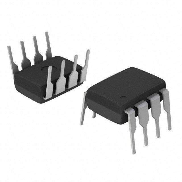
| 描述 | TVS ARRAY ESD 6 INPUT 30V 8-DIPTVS二极管阵列 6 CH DIODE ARRAY |
| 产品分类 | TVS - 其它复合分离式半导体 |
| 品牌 | Littelfuse |
| 产品手册 | |
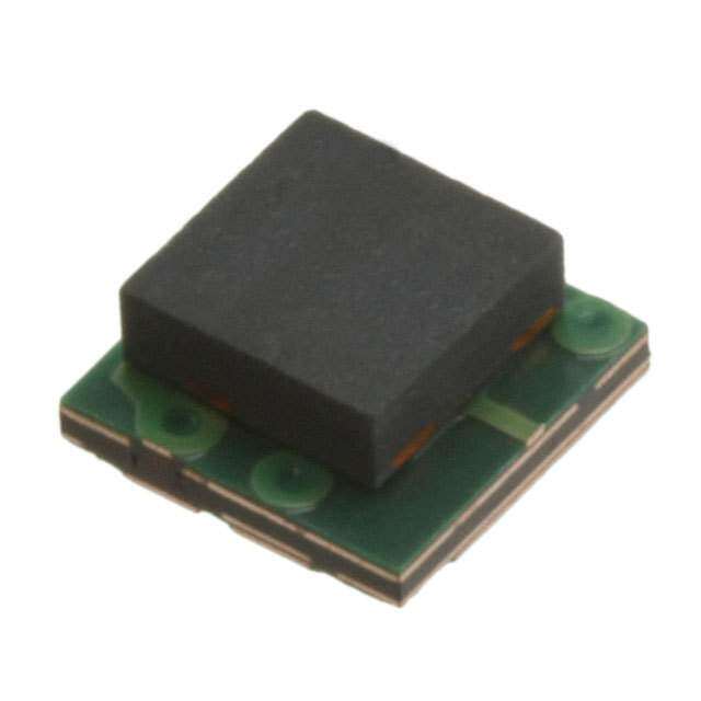
| 产品图片 |
|
| rohs | 符合RoHS无铅 / 符合限制有害物质指令(RoHS)规范要求 |
| 产品系列 | 二极管与整流器,TVS二极管,TVS二极管阵列,Littelfuse SP721APP- |
| 数据手册 | |
| 产品型号 | SP721APP |
| 产品培训模块 | http://www.digikey.cn/PTM/IndividualPTM.page?site=cn&lang=zhs&ptm=25590 |
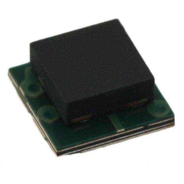
| 产品目录绘图 |
|
| 产品目录页面 | |
| 产品种类 | TVS二极管阵列 |
| 供应商器件封装 | 8-PDIP |
| 其它名称 | F2720 |
| 击穿电压 | 30 V |
| 功率(W) | - |
| 包装 | 管件 |
| 商标 | Littelfuse |
| 安装风格 | SMD/SMT |
| 封装 | Tube |
| 封装/外壳 | 8-DIP(0.300",7.62mm) |
| 封装/箱体 | PDIP-8 |
| 尺寸 | 7.11 mm W x 10.16 mm L x 4.95 mm H |
| 峰值浪涌电流 | 3 A |
| 工作电压 | 2 V to 30 V |
| 工厂包装数量 | 500 |
| 应用 | 通用 |
| 技术 | 混合技术 |
| 最大工作温度 | + 105 C |
| 最小工作温度 | - 40 C |
| 极性 | Bidirectional |
| 标准包装 | 50 |
| 电压-工作 | 30V |
| 电压-箝位 | - |
| 电容 | 3 pF |
| 电路数 | 6 |
| 端接类型 | SMD/SMT |
| 系列 | SP721 SPA |
| 通道 | 6 Channels |


- 商务部:美国ITC正式对集成电路等产品启动337调查
- 曝三星4nm工艺存在良率问题 高通将骁龙8 Gen1或转产台积电
- 太阳诱电将投资9.5亿元在常州建新厂生产MLCC 预计2023年完工
- 英特尔发布欧洲新工厂建设计划 深化IDM 2.0 战略
- 台积电先进制程称霸业界 有大客户加持明年业绩稳了
- 达到5530亿美元!SIA预计今年全球半导体销售额将创下新高
- 英特尔拟将自动驾驶子公司Mobileye上市 估值或超500亿美元
- 三星加码芯片和SET,合并消费电子和移动部门,撤换高东真等 CEO
- 三星电子宣布重大人事变动 还合并消费电子和移动部门
- 海关总署:前11个月进口集成电路产品价值2.52万亿元 增长14.8%


PDF Datasheet 数据手册内容提取
TVS Diode Arrays (SPA® Diodes) General Purpose ESD Protection - SP721 Series SP721 Series 3pF 4kV Diode Array RoHS Pb GREEN Description The SP721 is an array of SCR/Diode bipolar structures for ESD and over-voltage protection to sensitive input circuits. The SP721 has 2 protection SCR/Diode device structures per input. There are a total of 6 available inputs that can be used to protect up to 6 external signal or bus lines. Over- voltage protection is from the IN (Pins 1 - 3 and Pins 5 - 7) to V+ or V-. The SCR structures are designed for fast triggering at a threshold of one +V diode threshold above V+ (Pin 8) or BE a -V diode threshold below V- (Pin 4). From an IN input, BE a clamp to V+ is activated if a transient pulse causes the input to be increased to a voltage level greater than one Pinout V above V+. A similar clamp to V- is activated if a negative BE pulse, one V less than V-, is applied to an IN input. BE Standard ESD Human Body Model (HBM) Capability is: IN 1 8 V+ SP721 (PDIP, SOIC) IN 2 7 IN Features TOP VIEW IN 3 6 IN • ESD Interface Capability for HBM Standards V- 4 5 IN - MIL STD 3015.7 .................................................15kV - IEC 61000-4-2, Direct Discharge, - Single Input ..........................................4kV (Level 2) Functional Block Diagram - Two Inputs in Parallel ............................8kV (Level 4) - IEC 61000-4-2, Air Discharge ...............15kV (Level 4) • High Peak Current Capability - IEC 61000-4-5 (8/20µs) .......................................±3A - Single Pulse, 100µs Pulse Width ........................±2A - Single Pulse, 4µs Pulse Width ............................±5A • Designed to Provide Over-Voltage Protection - Single-Ended Voltage Range to ........................+30V - Differential Voltage Range to ............................±15V • Fast Switching .............................................2ns Rise Time • Low Input Leakages ............................1nA at 25ºC Typical • Low Input Capacitance .....................................3pF Typical • An Array of 6 SCR/Diode Pairs • Operating Temperature Range....................-40ºC to 105ºC Additional Information Applications • Microprocessor/Logic • Analog Device Input Input Protection Protection • Data Bus Protection • Voltage Clamp Resources Samples © 2017 Littelfuse, Inc. Specifications are subject to change without notice. Revised: 05/12/17
TVS Diode Arrays (SPA® Diodes) General Purpose ESD Protection - SP721 Series Absolute Maximum Ratings Thermal Information Parameter Rating Units Parameter Rating Units Continuous Supply Voltage, (V+) - (V-) +35 V Thermal Resistance (Typical, Note 1) θ oC/W JA Forward Peak Current, I to V , I to GND PDIP Package 160 oC/W IN CC IN ±2, 100µs A (Refer to Figure 5) SOIC Package 170 oC/W CAUTION: Stresses above those listed in “Absolute Maximum Ratings” may cause Maximum Storage Temperature Range -65 to 150 oC permanent damage to the device. This is a stress only rating and operation of the device at these or any other conditions above those indicated in the operational sections of this Maximum Junction Temperature (Plastic 150 oC specification is not implied. Package) Note: Maximum Lead Temperature 260 oC ESD Ratings and Capability (Figure 1, Table 1) (Soldering 20-40s)(SOIC Lead Tips Only) Load Dump and Reverse Battery (Note 2) 1. θ is measured with the component mounted on an evaluation PC board in free air. JA Electrical Characteristics T = -40oC to 105oC, V = 0.5V , Unless Otherwise Specified A IN CC Parameter Symbol Test Conditions Min Typ Max Units Operating Voltage Range, V - 2 to 30 - V SUPPLY V = [(V+) - (V-)] SUPPLY Forward Voltage Drop IN to V- V I = 1A (Peak Pulse) - 2 - V FWDL IN IN to V+ V - 2 - V FWDH Input Leakage Current I -20 5 +20 nA IN Quiescent Supply Current I - 50 200 nA QUIESCENT Equivalent SCR ON Threshold Note 3 - 1.1 - V Equivalent SCR ON Resistance V /I ; Note 3 - 1 - Ω FWD FWD Input Capacitance C - 3 - pF IN Input Switching Speed t - 2 - ns ON Notes: 2. In automotive and battery operated systems, the power supply lines should be externally protected for load dump and reverse battery. When the V+ and V- Pins are connected to het same supply voltage source as the device or control line under protection, a current limiti ng resistor should be connected in series between the external supply and the SP721 supply pins to limit reverse battery current to within the rated maximum limits. Bypass capacitors of typically 0.01µF or larger romf the V+ and V- Pins to ground are recommended. 3. Refer to the Figure 3 graph for definitions of equivalent “SCR ON Threshold” and “SCR ON Resistance”. These characteristics are given here for thumb-rule nformation to determine peak current and dissipation under EOS conditions. Typical Application of the SP721 (Application as an Input Clamp for Over-voltage, Greater than 1V Above V+ or less than -1V below V-) BE BE © 2017 Littelfuse, Inc. Specifications are subject to change without notice. Revised: 05/12/17
TVS Diode Arrays (SPA® Diodes) General Purpose ESD Protection - SP721 Series ESD Capability ESD capability is dependent on the application and defined Figure 1: Electrostatic Discharge Test test standard.The evaluation results for various test standards and methods based on Figure 1 are shown in Table 1. For the “Modified”MIL-STD-3015.7 condition that is defined as an “in-circuit” method of ESD testing, the V+ and V- pins have a return path to ground and the SP721 ESD capability is typically greater than 15kV from 100pF through 1.5kΩ.By strict definition of MIL-STD-3015.7 using “pin-to-pin”device testing, the ESD voltage capability is greater than 6kV.The MIL-STD-3015.7 results were determined from AT&T ESD Test Lab measurements. The HBM capability to the IEC 61000-4-2 standard is Table 1: ESD Test Conditions greater than 15kV for air discharge (Level 4) and greater than 4kV for direct discharge (Level 2).Dual pin capability (2 Standard Type/Mode R C ±V adjacent pins in parallel) is well in excess of 8kV (Level 4). D D D Modified HBM 1.5kΩ 100pF 15kV MIL STD 3015.7 For ESD testing of the SP721 to EIAJ IC121 Machine Standard HBM 1.5kΩ 100pF 6kV Model (MM) standard, the results are typically better than HBM, Air Discharge 330Ω 150pF 15kV 1kV from 200pF with no series resistance. HBM, Direct Discharge 330Ω 150pF 4kV IEC 61000-4-2 HBM, Direct Discharge, 330Ω 150pF 8kV Two Parallel Input Pins EIAJ IC121 Machine Model 0kΩ 200pF 1kV Figure 2: Low Current SCR Forward Voltage Drop Curve Figure 3: High Current SCR Forward Voltage Drop Curve © 2017 Littelfuse, Inc. Specifications are subject to change without notice. Revised: 05/12/17
TVS Diode Arrays (SPA® Diodes) General Purpose ESD Protection - SP721 Series Peak Transient Current Capability of the SP721 The peak transient current capability rises sharply as the Figure 4: Typical SP721 Peak Current Test Circuit width of the current pulse narrows. Destructive testing with a Variable Pulse Width Input was done to fully evaluate the SP721’s ability to withstand a wide range of peak current pulses vs time. The circuit used to generate current pulses is shown in Figure 4. The test circuit of Figure 4 is shown with a positive pulse input. For a negative pulse input, the (-) current pulse input goes to an SP721 ‘IN’ input pin and the (+) current pulse input goes to the SP721 V- pin. The V+ to V- supply of the SP721 must be allowed to float. (i.e., It is not tied to the ground reference of the current pulse generator.) Figure 5 shows the point of overstress as defined by increased leakage in excess of the data sheet published limits. The maximum peak input current capability is dependent on the ambient temperature, improving as the temperature is reduced. Peak current curves are shown for ambient Figure 5: SP721 Typical Single Peak Current Pulse temperatures of 25ºC and 105ºC and a 15V power supply Capability condition. The safe operating range of the transient peak Showing the Measured Point of Overstress in Amperes vs current should be limited to no more than 75% of the pulse width time in milliseconds measured overstress level for any given pulse width as shown in the curves of Figure 5. 7 CAUTION: SAFE OPERATING CONDITIONS LIMIT Note that adjacent input pins of the SP721 may be 6 THE MAXIMUM PEAK CURRENT FOR A GIVEN psuarsatlaleinleedd tpoe iamk pcruorvreen ctu crraepnatb (ialitnyd i sE SinDc)r ecaaspeadb itlioty n. eTahrely ENT (A) 54 TA = 25°C V+ TPOOUF LVTS-HSEEU W VPAIPDLLTUYH E= TS 1O S5 VHBEO WNON GORNE EAATECRH TCHUARNV E75.% R twice that of a single pin. CUR 3 TA = 105°C K A 2 E P 1 0 0.001 0.01 0.1 1 10 100 1000 PULSE WIDTH TIME (ms) © 2017 Littelfuse, Inc. Specifications are subject to change without notice. Revised: 05/12/17
TVS Diode Arrays (SPA® Diodes) General Purpose ESD Protection - SP721 Series Soldering Parameters Reflow Condition Pb – Free assembly - Temperature Min (T ) 150°C s(min) Pre Heat - Temperature Max (T ) 200°C s(max) - Time (min to max) (t) 60 – 180 secs s Average ramp up rate (Liquidus) Temp 5°C/second max (T) to peak L T to T - Ramp-up Rate 5°C/second max S(max) L - Temperature (T) (Liquidus) 217°C Reflow L - Temperature (t) 60 – 150 seconds L Peak Temperature (T ) 260+0/-5 °C P Time within 5°C of actual peak 20 – 40 seconds Temperature (t ) p Ramp-down Rate 5°C/second max Time 25°C to peak Temperature (T ) 8 minutes Max. P Do not exceed 260°C Package Dimensions — Dual-In-Line Plastic Packages (PDIP) Package PDIP Pins 8 Lead Dual-in-Line JEDEC MS-001 Millimeters Inches Notes Min Max Min Max A - 5.33 - 0.210 4 A1 0.39 - 0.015 - 4 A2 2.93 4.95 0.115 0.195 - B 0.356 0.558 0.014 0.022 - B1 1.15 1.77 0.045 0.070 8, 10 C 0.204 0.355 0.008 0.014 - Notes: D 9.01 10.16 0.355 0.400 5 1. Controlling Dimensions: INCH. In case of conflict between English and Metric D1 0.13 - 0.005 - 5 dimensions, the inch dimensions control. E 7.62 8.25 0.300 0.325 6 2. Dimensioning and tolerancing per ANSI Y14.5M-1982. 3. Symbols are defined in the “MO Series Symbol List” in Section 2.2 of Publication No. E1 6.10 7.11 0.240 0.280 5 95. e 2.54 BSC 0.100 BSC - 4. Dimensions A, A1 and L are measured with the package seated in JEDEC seating plane gauge GS-3. eA 7.62 BSC 0.300 BSC 6 5. D, D1, and E1 dimensions do not include mold flash or protrusions. Mold flash or e - 10.92 - 0.430 7 B protrusions shall not exceed 0.010 inch (0.25mm). L 2.93 3.81 0.115 0.150 4 6. E and e are measured with the leads constrained to be perpendicular to datum -C- . A N 8 8 9 7. e and e are measured at the lead tips with the leads unconstrained. e must be zero B C C or greater. 8. B1 maximum dimensions do not include dambar protrusions. Dambar protrusions shall not exceed 0.010 inch (0.25mm). 9. N is t he maximum number of terminal positions. 10. Corner leads (1, N, N/2 and N/2 + 1) for E8.3, E16.3, E18.3, E28.3, E42.6 will have a B1 dimension of 0.030 - 0.045 inch (0.76 - 1.14mm). © 2017 Littelfuse, Inc. Specifications are subject to change without notice. Revised: 05/12/17
TVS Diode Arrays (SPA® Diodes) General Purpose ESD Protection - SP721 Series Package Dimensions — Small Outline Plastic Packages (SOIC) N Package SOIC IANRDEEAX H 0.25(0.010) M B M Pins 8 E -B- JEDEC MS-012 Millimeters Inches 1 2 3 L Notes Min Max Min Max SEATING PLANE A 1.35 1.75 0.0532 0.0688 - -A- D A h x 45o A1 0.10 0.25 0.0040 0.0098 - -C- B 0.33 0.51 0.013 0.020 9 μ e A1 C 0.19 0.25 0.0075 0.0098 - C B 0.10(0.004) D 4.80 5.00 0.1890 0.1968 3 0.25(0.010) M C AM B S E 3.80 4.00 0.1497 0.1574 4 Notes: e 1.27 BSC 0.050 BSC - 1. Symbols are defined in the “MO Series Symbol List” in Section 2.2 of Publication NumbNeOr T9E5S.: H 5.80 6.20 0.2284 0.2440 - 2. Dimensioning and tolerancing per ANSI Y14.5M-1982. 1. Symbolsa re definedi n the “MOS eries SymbolL ist”i n Section 2.2 of h 0.25 0.50 0.0099 0.0196 5 3. DimensionP u“bDl”ic adtoieosn N noutm inbcelur9 d5e. mold flash, protrusions or gate burrs. Mold flash, protrus2io.nD aimnde gnastieo nbiunrgras n sdh taolll enroat necxicnegep de r0 A.1N5mSIm Y 1(40..50M06- 1in9c8h2). per side. L 0.40 1.27 0.016 0.050 6 4. Dimen3s.ioDn i“mEe”n dsoioens“ nDo”td ioneclsu ndoet i inntcelruledaedm floalsdhfl aosr hp,r portroutsruiosniso.n Isno tre gr-aletead b uflarrssh. and protrusionMs oshldafl lla nsoht, pexrocetreuds i0o.n2a5 nmdm ga (t0e. 0b1u0r risns chh)a plle nro st iedxec.eed 0.15mm (0.006 N 8 8 7 5. The chamifnecr ho)n p tehre s ibdoed.y is optional. If it is not present, a visual index feature must be located4 .wDithimine tnhsei ocnro“ sEs”hd aotechse ndo at irnecal.ude interleadfl ash or protrusions.I nter- µ 0º 8º 0º 8º - 6. “L” is the lleeandg tflha osfh t aenrmd ipnraol tfrours sioolndses rhinagll ntoo at e sxucbesetdra 0te.2.5mm (0.010 inch) per 7. “N” is thes induem.ber of terminal positions. Product Characteristics 5.The chamfer on the body is optional.I f it is not present, a visual index 8. Terminal numbers are shown for reference only. feature must be located withint he crosshatcheda rea. 9. The lead width “B”, as measured 0.36mm (0.014 inch) or greater above the seating 6. “L” is the length of terminalf or solderingt o a substrate. plane, shall not exceed a maximum value of 0.61mm (0.024 inch). Lead Plating Matte Tin 7. “N”i s the numbero f terminalp ositions. 10. Controlling dimension: MILLIMETER. Converted inch dimensions are not necessarily exact.8.Terminal numbersa re shown for reference only. 9.The lead width“ B”, as measured0 .36mm (0.014 inch) or greater Lead Material Copper Alloy above the seating plane, shall not exceed a maximum value of Part Nu0m.61bmemr (i0n.0g24 Sinychs).tem Lead Coplanarity 0.004 inches (0.102mm) 10. Controllingd imension:MILLIMETER. Convertedi nch dimensions are not necessarilye xact. Substitute Material Silicon SP 721** ** Body Material Molded Epoxy T(SVPSA D® iDoidoed Aesr)rays GP == LGeraede nFree Flammability UL 94 V-0 TG= Tape and Reel Package Series AB = 8 Ld SOIC AP = 8 Ld PDIP Ordering Information Environmental Part Number Temp. Range (ºC) Package Marking Min. Order Informaton SP721APP -40 to 105 8 Ld PDIP Lead-free SP721AP(P) 1 2000 SP721ABG -40 to 105 8 Ld SOIC Green SP721A(B)G 2 1960 SP721ABTG -40 to 105 8 Ld SOIC Tape and Reel Green SP721A(B)G 2 2500 Notes: 1. SP721AP(P) means device marking either SP721AP or SP721APP. 2. SP721A(B)G means device marking either SP721AG or SP721ABG which are good for types SP721ABG and SP721ABTG. Disclaimer Notice - Information furnished is believed to be accurate and reliable. However, users should independently evaluate the suitability of and test each product selected for their own applications. Littelfuse products are not designed for, and may not be used in, all applications. Read complete Disclaimer Notice at www.littelfuse.com/disclaimer-electronics. © 2017 Littelfuse, Inc. Specifications are subject to change without notice. Revised: 05/12/17