ICGOO在线商城 > 电路保护 > TVS - 混合技术 > ZEN056V230A16LS
 Datasheet下载
- 型号: ZEN056V230A16LS
- 制造商: CORCOM/TYCO ELECTRONICS
- 库位|库存: xxxx|xxxx
- 要求:
| 数量阶梯 | 香港交货 | 国内含税 |
| +xxxx | $xxxx | ¥xxxx |
查看当月历史价格
查看今年历史价格
ZEN056V230A16LS产品简介:
ICGOO电子元器件商城为您提供ZEN056V230A16LS由CORCOM/TYCO ELECTRONICS设计生产,在icgoo商城现货销售,并且可以通过原厂、代理商等渠道进行代购。 ZEN056V230A16LS价格参考。CORCOM/TYCO ELECTRONICSZEN056V230A16LS封装/规格:TVS - 混合技术, 。您可以下载ZEN056V230A16LS参考资料、Datasheet数据手册功能说明书,资料中有ZEN056V230A16LS 详细功能的应用电路图电压和使用方法及教程。
Littelfuse Inc. 的 ZEN056V230A16LS 是一款 TVS(瞬态电压抑制器)二极管,属于混合技术类别。该型号主要用于保护电子设备免受瞬态电压的损害,例如静电放电(ESD)、雷击感应浪涌和电路开关引起的过压事件。

以下是 ZEN056V230A16LS 的主要应用场景:

1. 通信设备:
   用于保护网络接口、调制解调器、路由器和交换机中的信号线路,防止因雷击或 ESD 引发的损坏。

2. 消费类电子产品:
   应用于电视、音响系统、家用电器等设备的电源和信号端口,提供过压保护,确保设备在复杂电磁环境下的稳定性。

3. 汽车电子系统:
   在车载信息娱乐系统、传感器模块和 CAN 总线中使用,抵御因负载突降或电气干扰导致的瞬态电压。

4. 工业控制设备:
   保护 PLC、变频器和自动化控制系统中的输入/输出端口,避免因恶劣工业环境中的浪涌或噪声引发故障。

5. 数据传输接口:
   适用于 USB、HDMI、以太网等高速数据接口,提供低电容特性的保护,同时保持信号完整性。

6. 电源模块保护:
   在 AC-DC 或 DC-DC 转换器中,防止因输入电压波动或外部干扰造成的损坏。

ZEN056V230A16LS 的特性使其特别适合需要高可靠性、快速响应和低箝位电压的应用场景。其混合技术设计结合了多种优势,能够在不影响系统性能的情况下提供卓越的保护能力。
| 参数 | 数值 |
| 产品目录 | |
| 描述 | POLYZEN 5.6V PPTC/ZENER SMDTVS 二极管 - 瞬态电压抑制器 5.6V .04W 2.3A LS SMD PolyZen DEVICES |
| 产品分类 | |
| 品牌 | TE Connectivity |
| 产品手册 | |
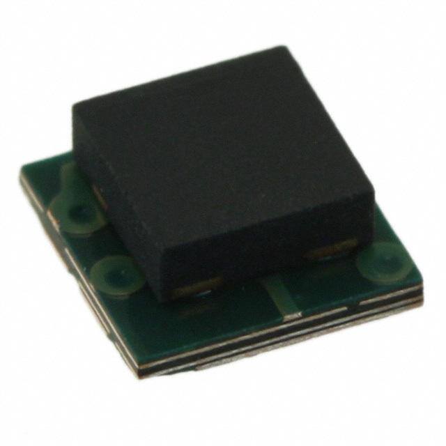
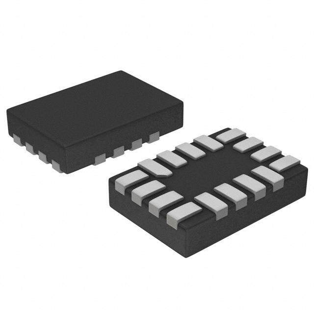
| 产品图片 |
|
| rohs | 符合RoHS无铅 / 符合限制有害物质指令(RoHS)规范要求 |
| 产品系列 | 二极管与整流器,TVS二极管,TVS 二极管 - 瞬态电压抑制器,TE Connectivity / Raychem ZEN056V230A16LSPolyZen,Raychem |
| 数据手册 | http://www.te.com/commerce/DocumentDelivery/DDEController?Action=srchrtrv&DocNm=CLP00002&DocType=CS&DocLang=Englishhttp://www.te.com/commerce/DocumentDelivery/DDEController?Action=srchrtrv&DocNm=SCD27327&DocType=SS&DocLang=EN |
| 产品型号 | ZEN056V230A16LS |
| 产品培训模块 | http://www.digikey.cn/PTM/IndividualPTM.page?site=cn&lang=zhs&ptm=6719http://www.digikey.cn/PTM/IndividualPTM.page?site=cn&lang=zhs&ptm=24704 |
| 产品目录绘图 |
|
| 产品目录页面 | |
| 产品种类 | TVS 二极管 - 瞬态电压抑制器 |
| 供应商器件封装 | SMD |
| 其它名称 | ZEN056V230A16LSDKR |
| 击穿电压 | 16 V |
| 功率(W) | 700mW |
| 包装 | Digi-Reel® |
| 商标 | TE Connectivity / Raychem |
| 安装风格 | SMD/SMT |
| 封装 | Reel |
| 封装/外壳 | 3-SMD,无引线 |
| 尺寸 | 4.15 mm W x 4.15 mm L x 2 mm H |
| 峰值浪涌电流 | 2.3 A |
| 峰值脉冲功率耗散 | 700 mW |
| 工作电压 | 5 V |
| 工厂包装数量 | 3000 |
| 应用 | 通用 |
| 技术 | 混合技术 |
| 最大工作温度 | + 85 C |
| 最小工作温度 | - 40 C |
| 标准包装 | 1 |
| 电压-工作 | 5.6V |
| 电压-箝位 | 16V |
| 电容 | 4200 pF |
| 电路数 | 1 |
| 端接类型 | SMD/SMT |
| 配用 | /product-detail/zh/ZEN056V230A16LS-TB/ZEN056V230A16LS-TB-ND/1858916 |
| 钳位电压 | 5.6 V |
| 零件号别名 | RF1491-000 |


- 商务部:美国ITC正式对集成电路等产品启动337调查
- 曝三星4nm工艺存在良率问题 高通将骁龙8 Gen1或转产台积电
- 太阳诱电将投资9.5亿元在常州建新厂生产MLCC 预计2023年完工
- 英特尔发布欧洲新工厂建设计划 深化IDM 2.0 战略
- 台积电先进制程称霸业界 有大客户加持明年业绩稳了
- 达到5530亿美元!SIA预计今年全球半导体销售额将创下新高
- 英特尔拟将自动驾驶子公司Mobileye上市 估值或超500亿美元
- 三星加码芯片和SET,合并消费电子和移动部门,撤换高东真等 CEO
- 三星电子宣布重大人事变动 还合并消费电子和移动部门
- 海关总署:前11个月进口集成电路产品价值2.52万亿元 增长14.8%


PDF Datasheet 数据手册内容提取
PRODUCT: ZEN056V230A16LS PolyZen DOCUMENT: SCD27327 Polymer Enhanced Zener Diode REV LETTER: F Micro-Assemblies REV DATE: JULY 26, 2016 PAGE NO.: 1 OF 9 Specification Status: Released GENERAL DESCRIPTION BENEFITS Littelfuse PolyZen devices are polymer Stable Zener diode helps shield enhanced, precision Zener diode micro- downstream electronics from overvoltage assemblies. They offer resettable and reverse bias protection against multi-Watt fault events without the need for multi-Watt heat sinks. Trip events shut out overvoltage and reverse bias sources The Zener diode used for voltage clamping in a PolyZen micro-assembly was selected Analog nature of trip events minimizes due to its relatively flat voltage vs current upstream inductive spikes response. This helps improve output voltage clamping, even Minimal power dissipation requirements when input voltage is high and diode currents are large. Single component placement An advanced feature of the PolyZen micro-assembly is that the FEATURES Zener diode is thermally coupled to a resistively non-linear, Overvoltage transient suppression polymer PTC (positive temperature coefficient) layer. This PTC layer is fully integrated into the device, and is electrically in Stable VZ vs fault current series between VIN and the diode clamped VOUT. Time delayed, overvoltage trip This advanced PTC layer responds to either extended diode Time delayed, reverse bias trip heating or overcurrent events by transitioning from a low to Multi-Watt power handling capability high resistance state, also known as” tripping”. A tripped PTC Integrated device construction will limit current and generate voltage drop. It helps to protect both the Zener diode and the follow on electronics and RoHS Compliant effectively increases the diode’s power handling capability. TARGET APPLICATIONS The polymer enhanced Zener diode helps protect sensitive DC power port protection in portable portable electronics from damage caused by inductive voltage electronics spikes, voltage transients, incorrect power supplies and DC power port protection for systems reverse bias. These devices are particularly suitable for using barrel jacks for power input portable electronics and other low-power DC devices. Internal overvoltage & transient suppression DC output voltage regulation TYPICAL APPLICATION BLOCK DIAGRAM PPPooowwweeerrr SSSuuupppppplllyyy PPPooolllyyyZZZeeennn PPPrrrooottteeecccttteeeddd EEEllleeeccctttrrrooonnniiicccsss (((EEExxxttteeerrrnnnaaalll ooorrr IIInnnttteeerrrnnnaaalll))) GGGNNNDDD 222 VVVIIINNN 111 PPoollyyZZeenn +++ DDeevviiccee VVV OOOUUUTTT 333 RRReeeggguuulllaaattteeeddd RRR LLLoooaaaddd OOOuuutttpppuuuttt PPPrrrooottteeecccttteeeddd dddooowwwnnnssstttrrreeeaaammm eeellleeeccctttrrrooonnniiicccsss © 2016 Littelfuse,Inc. littelfuse.com Specifications are subject to change without notice. Revised July 26,2016
PRODUCT: ZEN056V230A16LS PolyZen DOCUMENT: SCD27327 Polymer Enhanced Zener Diode REV LETTER: F Micro-Assemblies REV DATE: JULY 26, 2016 PAGE NO.: 2 OF 9 CONFIGURATION INFORMATION Pin Configuration (Top View) Recommended Pad Dimensions 00..9944 mmmm 2 GND ((00..003377””)) 22..2211 mmmm 00..3333 mmmm VIN 1 ((00..008877””)) ((00..001133 ””)) 00..9944 mmmm 3 V ((00..003377””)) OUT 00..5566 mmmm 22..8888 mmmm 00..5566 mmmm ((00..002222””)) ((00..11113355””)) ((00..002222””)) PIN DESCRIPTION Pin Number Pin Name Pin Function 1 V V . Protected input to Zener diode. IN IN 2 GND GND 3 V V . Zener regulated voltage output OUT OUT BLOCK DIAGRAM PPoollyymmeerr PPTTCC VV IINN VV OOUUTT ZZeenneerr DDiiooddee GGNNDD DEFINITION of TERMS II II PPTTCC OOUUTT I Current flowing through the PTC portion of the PTC circuit VV IFLT RMS fault current flowing through the diode IINN I Current flowing out the V pin of the device OUT OUT VV Trip Event A condition where the PTC transitions to a high OOUUTT resistance state, thereby significantly limiting I II PTC FFLLTT and related currents, and significantly increasing the voltage drop between V and V . IN OUT Trip Time the PTC portion of the device remains both Endurance powered and in a tripped state. GGNNDD © 2016 Littelfuse,Inc. littelfuse.com Specifications are subject to change without notice. Revised July 26,2016
PRODUCT: ZEN056V230A16LS PolyZen DOCUMENT: SCD27327 Polymer Enhanced Zener Diode REV LETTER: F Micro-Assemblies REV DATE: JULY 26, 2016 PAGE NO.: 3 OF 9 GENERAL SPECIFICATIONS Operating Temperature -40º to +85ºC Storage Temperature -40º to +85ºC ELECTRICAL CHARACTERISTICS1-3, 11 (Typical unless otherwise specified) V(VZ )4 I 5 Leakage Current VInt( VM )a x8 IFLT Max9 TDriipspseiMpdaa xPti oo nw 1e 0 r I 4 HOLD R Typ6 R 7 (Azt) @2(A0º)C Max (Ohms) (Oh1Mmaxs) MVIaNxT Test IFLT Test Value Test Test Current Max Voltage Voltage Min Typ Max Current (V) (W) Voltage (A) (A) (V) (V) (mA) +5 +16 5.45 5.6 5.75 0.1 2.3 5.25 10 0.04 0.06 16V 5A 1.0 16 -40 -12V Note 1: Electrical characteristics determined at 25ºC unless otherwise specified. Note 2:This device is intended for limited fault protection. Repeated trip events or extended trip endurance can degrade the device and may affect performance to specifications. Performance impact will depend on multiple factors including, but not limited to, voltage, trip current, trip duration, trip cycles, and circuit design. For details or ratings specific to your application contact Littelfuse Circuit Protection directly. Note 3:Specifications developed using 1.0 ounce 0.045” wide copper traces on dedicated FR4 test boards. Performance in your application may vary. Note 4:Izt is the current at which Vz is measured (VZ = VOUT). Additional VZ values are available on request. Note 5:IHOLD : Maximum steady state IPTC (current entering or exiting the VIN pin of the device) that will not generate a trip event at the specified temperature. Specification assumes IFLT (current flowing through the Zener diode) is sufficiently low so as to prevent the diode from acting as a heat source. Testing is conducted with an “open” Zener. Note 6:R Typ: Resistance between VIN and VOUT pins during normal operation at room temperature. Note 7:R1Max: The maximum resistance between VIN and VOUT pins at room temperature, one hour after 1st trip or after reflow soldering. Note 8:VINT Max: VINT Max relates to the voltage across the PPTC portion of the PolyZen device (VIN-VOUT). VINT Max is defined as the voltage (VIN-VOUT) at which typical qualification devices (98% devices, 95% confidence) survived at least 100 trip cycles and 24 hours trip endurance at the specified voltage (VIN-VOUT) and current (IPTC). VINT Max testing is conducted using a "shorted" load (VOUT = 0V). VINT Max is a survivability rating, not a performance rating. Note 9:IFLT Max: IFLT Max relates to the stead state current flowing through the diode portion of the PolyZen device in a fault condition, prior to a trip event. IFLT Max is defined as the current at which typical qualification devices (12 parts per lot from 3 lots) survived 100 test cycles. RMS fault currents above IFLT Max may permanently damage the diode portion of the PolyZen device. Testing is conducted with NO load connected to VOUT, such that IOUT = 0. “Test voltage” is defined as the voltage between VIN to GND and includes the PolyZen Diode drop. Specification is dependent on the direction of current flow through the diode. IFLT Max is a survivability rating, not a performance rating. Note 10:The power dissipated by the device when in the “tripped” state, as measured on Littelfuse test boards (see note 3). Note 11:Specifications based on limited qualification data and subject to change. © 2016 Littelfuse,Inc. littelfuse.com Specifications are subject to change without notice. Revised July 26,2016
PRODUCT: ZEN056V230A16LS PolyZen DOCUMENT: SCD27327 Polymer Enhanced Zener Diode REV LETTER: F Micro-Assemblies REV DATE: JULY 26, 2016 PAGE NO.: 4 OF 9 MECHANICAL DIMENSIONS Min Typical Max 4.15 3.85 mm 4 mm Length L mm (0.152”) (0.16”) (0.163") 4.15 3.85 mm 4 mm Width W mm (0.152”) (0.16”) (0.163") 1.4mm 1.7 mm 2.0 mm Height H (0.055”) (0.067”) (0.081”) Length 3.0 mm Ld - - Diode (0.118”) Height 1.0 mm Hd - - Diode (0.039”) 0.6 mm Offset O1 - - (0.024”) 0.7 mm Offset O2 - - (0.028”) SOLDER REFLOW RECOMMENDATIONS: Classification Reflow Profiles Profile Feature Pb-Free Assembly Average Ramp-Up Rate (Tsmax to Tp) 3° C/second max. Preheat • Temperature Min (Tsmin) 150 °C • Temperature Max (Tsmax) 200 °C • Time (tsmin to tsmax) 60-180 seconds Time maintained above: • Temperature (TL) 217 °C • Time (tL) 60-150 seconds Peak/Classification Temperature (Tp) 260 °C Time within 5 °C of actual Peak Temperature (tp) 20-40 seconds Ramp-Down Rate 6 °C/second max. Time 25 °C to Peak Temperature 8 minutes max. © 2016 Littelfuse,Inc. littelfuse.com Specifications are subject to change without notice. Revised July 26,2016
PRODUCT: ZEN056V230A16LS PolyZen DOCUMENT: SCD27327 Polymer Enhanced Zener Diode REV LETTER: F Micro-Assemblies REV DATE: JULY 26, 2016 PAGE NO.: 5 OF 9 PACKAGING Packaging Tape & Reel Standard Box ZENXXXVXXXAXXLS 3,000 15,000 Reel Dimensions for PolyZen Devices A = 330 max N = 102 min W = 8.4 1 W = 11.1 2 MMaattttee FFiinniisshh TThheessee AArreeaa NNmmiinn AAmmaaxx © 2016 Littelfuse,Inc. littelfuse.com Specifications are subject to change without notice. Revised July 26,2016
PRODUCT: ZEN056V230A16LS PolyZen DOCUMENT: SCD27327 Polymer Enhanced Zener Diode REV LETTER: F Micro-Assemblies REV DATE: JULY 26, 2016 PAGE NO.: 6 OF 9 Taped Component Dimensions for PolyZen Devices TYPICAL CHARACTERISTICS © 2016 Littelfuse,Inc. littelfuse.com Specifications are subject to change without notice. Revised July 26,2016
PRODUCT: ZEN056V230A16LS PolyZen DOCUMENT: SCD27327 Polymer Enhanced Zener Diode REV LETTER: F Micro-Assemblies REV DATE: JULY 26, 2016 PAGE NO.: 7 OF 9 Typical Fault Response: ZEN056V230A16LS 16V, 5.0A Current Limited Source (I = 0) OUT 20 Vin (V) ) Vout (V) A15 I FLT (A) ( I r o10 ) V ( 5 V 0 0.00 0.04 0.08 0.12 0.16 0.20 Time (s) Pulse IV (300uSec Pulse) Pulse IV (300uSec Pulse) 8 10 V) 7 ZEN056VxxxAxxLS ( UT 6 A) 5 age: VO 45 nt: I (FLT 0 Volt 3 urre C -5 2 ZEN056VxxxAxxLS 0 0 0 0 0 1 .0 .0 .0 .0 .1 -10 0 0 0 1 00 01 1 -2 0 2 4 6 8 1 Current: IFLT (A) Voltage: VOUT (V) VOUT Peak Vs IFLT RMS (IOUT = 0) Time to Trip Vs IFLT RMS (IOUT = 0) 1.E+02 7.0 ZEN056V230A16LS 6.5 c) ) e 1.E+01 V S k ( 6.0 p ( ea 5.5 Tri 1.E+00 PT To OU 5.0 e V ZEN056V230A16LS m 1.E-01 4.5 Ti 4.0 1.E-02 0 1 2 3 4 5 0 1 2 3 4 5 IFLT RMS(A) IFLT RMS (A) © 2016 Littelfuse,Inc. littelfuse.com Specifications are subject to change without notice. Revised July 26,2016
PRODUCT: ZEN056V230A16LS PolyZen DOCUMENT: SCD27327 Polymer Enhanced Zener Diode REV LETTER: F Micro-Assemblies REV DATE: JULY 26, 2016 PAGE NO.: 8 OF 9 Time to Trip Vs I (I = 0) V Peak Vs I (I = 0) FLT OUT OUT FLT OUT 0.00 100.00 -0.20 ZENxxxV230A16LS c) 10.00 ZENxxxV230A16LS e S -0.40 ( V) p 1.00 ( ri T -0.60 T VOU -0.80 e To 0.10 m -1.00 Ti 0.01 -1.20 0.00 -50 -40 -30 -20 -10 0 -50 -40 -30 -20 -10 0 IFLT RMS(A) IFLT RMS (A) Temperature Effect on I (I = 0) Time to Trip Vs IPTC (IFLT = 0) Hold FLT 1000 4.0 ZEN056V230A16LS ZENxxxV230A16LS c) 100 e 3.0 S Linear ( 10 ) p A (ZENxxxV230A16LS) ri (old 2.0 To T 1 IH e 0.1 1.0 m Ti 0.01 0.0 0.001 -40 -20 0 20 40 60 80 100 0 10 20 30 40 Ambient Temperature (C) I RMS (A) PTC © 2016 Littelfuse,Inc. littelfuse.com Specifications are subject to change without notice. Revised July 26,2016
PRODUCT: ZEN056V230A16LS PolyZen DOCUMENT: SCD27327 Polymer Enhanced Zener Diode REV LETTER: F Micro-Assemblies REV DATE: JULY 26, 2016 PAGE NO.: 9 OF 9 Temperature Effect on R Typ 0.10 ZEN056V230A16LS ) 0.08 s m h O 0.05 ( p y T R 0.03 0.00 20 40 60 80 Ambient Temperature (C) Materials Information ROHS Compliant ELV Compliant Pb-Free Halogen Free* HF * Halogen Free refers to: Br≤900ppm, Cl≤900ppm, Br+Cl≤1500ppm. Littelfuse products are not designed for, and shall not be used for, any purpose (including, without limitation, automotive, military, aerospace, medical, life-saving, life- sustaining or nuclear facility applications, devices intended for surgical implant into the body, or any other application in which the failure or lack of desired operation of the product may result in personal injury, death, or property damage) other than those expressly set forth in applicable Littelfuse product documentation. Warranties granted by Littelfuse shall be deemed void for products used for any purpose not expressly set forth in applicable Littelfuse documentation. Littelfuse shall not be liable for any claims or damages arising out of products used in applications not expressly intended by Littelfuse as set forth in applicable Littelfuse documentation. The sale and use of Littelfuse products is subject to Littlefuse Terms and Conditions of Sale, unless otherwise agreed by Littelfuse © 2016 Littelfuse,Inc. littelfuse.com Specifications are subject to change without notice. Revised July 26,2016