ICGOO在线商城 > 电路保护 > TVS - 混合技术 > CM2009-02QR

 Datasheet下载
- 型号: CM2009-02QR
- 制造商: ON Semiconductor
- 库位|库存: xxxx|xxxx
- 要求:
| 数量阶梯 | 香港交货 | 国内含税 |
| +xxxx | $xxxx | ¥xxxx |
查看当月历史价格
查看今年历史价格
CM2009-02QR产品简介:
ICGOO电子元器件商城为您提供CM2009-02QR由ON Semiconductor设计生产,在icgoo商城现货销售,并且可以通过原厂、代理商等渠道进行代购。 CM2009-02QR价格参考¥询价-¥询价。ON SemiconductorCM2009-02QR封装/规格:TVS - 混合技术, 。您可以下载CM2009-02QR参考资料、Datasheet数据手册功能说明书,资料中有CM2009-02QR 详细功能的应用电路图电压和使用方法及教程。
型号为CM2009-02QR、品牌为ON Semiconductor的TVS(瞬态电压抑制器)属于混合技术保护器件,主要用于电子电路中的过压和ESD(静电放电)防护。该器件集成了TVS二极管和可控硅(SCR)等技术,兼具快速响应与高浪涌承受能力,适用于对可靠性要求较高的场景。

典型应用场景包括:便携式消费类电子产品(如智能手机、平板电脑、可穿戴设备)中的USB接口、音频接口及充电端口的ESD保护;工业控制设备中通信端口(如RS-232、RS-485)的瞬态干扰抑制;以及汽车电子系统中的低速信号线保护(如车载信息娱乐系统的数据线路)。此外,也常用于电源管理模块和传感器接口,防止因静电或电压突变导致的芯片损坏。

CM2009-02QR采用小型化封装(如SOD-962),节省PCB空间,适合高密度布局设计;其低电容特性确保了高速信号传输的完整性,不会影响正常通信性能。工作温度范围宽,适应严苛环境,具备良好的长期稳定性。

综上,CM2009-02QR广泛应用于消费电子、工业控制和汽车电子等领域,为敏感电路提供高效、可靠的双向过压和ESD保护,是现代电子系统中重要的前端防护元件。
| 参数 | 数值 |
| 产品目录 | |
| 描述 | DIODE VGA PORT COMPANION 16-QSOP视频 IC VGA Port Circuit 15 Ohm |
| 产品分类 | TVS - 其它复合集成电路 - IC |
| 品牌 | ON Semiconductor |
| 产品手册 | |
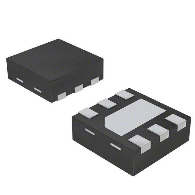
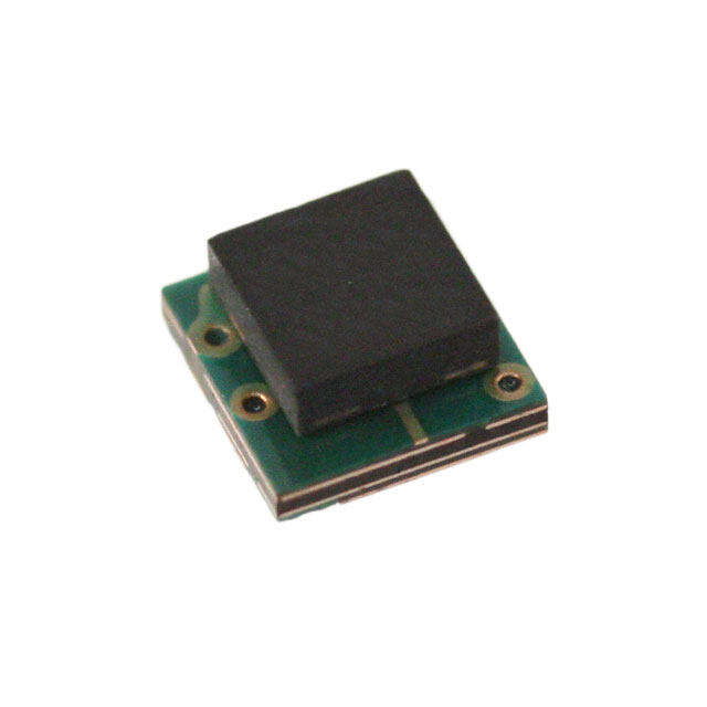
| 产品图片 |
|
| rohs | 符合RoHS无铅 / 符合限制有害物质指令(RoHS)规范要求 |
| 产品系列 | 多媒体 IC,视频 IC,ON Semiconductor CM2009-02QR- |
| 数据手册 | |
| 产品型号 | CM2009-02QR |
| 产品种类 | 视频 IC |
| 供应商器件封装 | 16-QSOP |
| 其它名称 | CM2009-02QROSDKR |
| 功率(W) | 500mW |
| 包装 | Digi-Reel® |
| 商标 | ON Semiconductor |
| 安装风格 | SMD/SMT |
| 封装 | Reel |
| 封装/外壳 | 16-SSOP(0.154",3.90mm 宽) |
| 封装/箱体 | QSOP-16 |
| 工作电源电压 | - 0.5 V to + 6 V |
| 工厂包装数量 | 2500 |
| 应用 | DVI-I、VGA 端口 |
| 技术 | 二极管阵列 |
| 最大工作温度 | + 85 C |
| 最小工作温度 | - 40 C |
| 标准包装 | 1 |
| 电压-工作 | 6V |
| 电压-箝位 | 6V |
| 电源电流 | 10 uA |
| 电路数 | 1 |
| 类型 | The CM2009 connects between a video graphics controller embedded in a PC, graphics adapter card or set top box and the VGA or DVI-I port connector. |
| 系列 | CM2009 |
| 通道数量 | 7 Channel |


- 商务部:美国ITC正式对集成电路等产品启动337调查
- 曝三星4nm工艺存在良率问题 高通将骁龙8 Gen1或转产台积电
- 太阳诱电将投资9.5亿元在常州建新厂生产MLCC 预计2023年完工
- 英特尔发布欧洲新工厂建设计划 深化IDM 2.0 战略
- 台积电先进制程称霸业界 有大客户加持明年业绩稳了
- 达到5530亿美元!SIA预计今年全球半导体销售额将创下新高
- 英特尔拟将自动驾驶子公司Mobileye上市 估值或超500亿美元
- 三星加码芯片和SET,合并消费电子和移动部门,撤换高东真等 CEO
- 三星电子宣布重大人事变动 还合并消费电子和移动部门
- 海关总署:前11个月进口集成电路产品价值2.52万亿元 增长14.8%


PDF Datasheet 数据手册内容提取
CM2009 VGA Port Companion Circuit Product Description The CM2009 connects between a video graphics controller embedded in a PC, graphics adapter card or set top box and the VGA http://onsemi.com or DVI−I port connector. The CM2009 incorporates ESD protection for all signals, level shifting for the DDC signals and buffering for the SYNC signals. ESD protection for the video, DDC and SYNC lines is implemented with low−capacitance current steering diodes. All ESD diodes are designed to safely handle the high current spikes specified by IEC−61000−4−2 Level 4 (±8 kV contact discharge if QSOP16 C is present, ±4 kV if not). The ESD protection for the DDC signal QR SUFFIX BYP pins are designed to prevent “back current” when the device is CASE 492 powered down while connected to a monitor that is powered up. Separate positive supply rails are provided for the VIDEO, DDC MARKING DIAGRAM and SYNC channels to facilitate interfacing with low voltage video controller ICs to provide design flexibility in multi−supply−voltage CMD YYWW environments. CM2009 Two non−inverting drivers provide buffering for the HSYNC and 0xQR VSYNC signals from the video controller IC (SYNC1, SYNC2). These buffers accept TTL input levels and convert them to CMOS output levels that swing between Ground and VCC_SYNC, which is CM20090xQR = Specific Device Code typically 5 V. Additionally, each driver has a series termination resistor YY = Year (R ) connected to the SYNC_OUT pin, eliminating the external WW = Work Week T termination resistors typically required for the HSYNC and VSYNC lines of the video cable. There are three versions with different values ORDERING INFORMATION of R to allow termination at typically 65 (cid:2) (CM2009−00) or 15 (cid:2) T (CM2009−02). Device Package Shipping† The 15 (cid:2) (CM2009−02) version will typically require two external CM2009−00QR QSOP−16 2500/Tape & Reel resistors which can be chosen to exactly match the characteristic (Pb−Free) impedance of the SYNC lines of the video cable. Two N−channel MOSFETs provide the level shifting function CM2009−02QR QSOP−16 2500/Tape & Reel (Pb−Free) required when the DDC controller is operated at a lower supply voltage than the monitor. The gate terminals for these MOSFETS †For information on tape and reel specifications, including part orientation and tape sizes, please (V ) should be connected to the supply rail (typically 3.3 V) CC_DDC refer to our Tape and Reel Packaging Specification that supplies power to the transceivers of the DDC controller. Brochure, BRD8011/D. Features • • Includes ESD Protection, Level−Shifting, Buffering and 5 V Drivers for HSYNC and VSYNC Lines Sync Impedance Matching • Integrated Impedance Matching Resistors on Sync Lines • 7 Channels of ESD Protection for all VGA Port • Bi−directional Level Shifting N−Channel FETs Connector Pins Meeting IEC−61000−4−2 Level 4 ESD Provided for DDC_CLK & DDC_DATA Channels Requirements (±8 kV Contact Discharge) • Backdrive Protection on DDC Lines • Very Low Loading Capacitance from ESD Protection • Compact 16−Lead QSOP Package Diodes on VIDEO Lines (4 pF Maximum) • These Devices are Pb−Free and are RoHS Compliant Applications • VGA and DVI−I Ports in: ♦ Desktop and Notebook PCs ♦ Graphics Cards ♦ Set Top Boxes © Semiconductor Components Industries, LLC, 2012 1 Publication Order Number: May, 2012 − Rev. 5 CM2009/D
CM2009 SIMPLIFIED ELECTRICAL SCHEMATIC 9 V DDC_OUT1 CC_VIDEO 12 DDC_OUT2 2 VCC_DDC BYP VCC_SYNC 7 8 1 3 VIDEO_1 4 VIDEO_2 VIDEO_3 5 RT RT 6 GND 16 SYNC_OUT2 14 SYNC_OUT1 GND 10 DDC_IN1 11 DDC_IN2 13 SYNC_IN1 15 SYNC_IN2 PACKAGE / PINOUT DIAGRAM Top View VCC_SYNC 1 16 SYNC_OUT2 VCC_VIDEO 2 15 SYNC_IN2 VIDEO_1 3 14 SYNC_OUT1 VIDEO_2 4 13 SYNC_IN1 VIDEO_3 5 12 DDC_OUT2 GND 6 11 DDC_IN2 VCC_DDC 7 10 DDC_IN1 BYP 8 9 DDC_OUT1 16 Pin QSOP Table 1. PIN DESCRIPTIONS Lead(s) Name Description 1 VCC_SYNC This is an isolated supply input for the SYNC_1 and SYNC_2 level shifters and their associated ESD protection circuits. 2 VCC_VIDEO This is a supply pin specifically for the VIDEO_1, VIDEO_2 and VIDEO_3 ESD protection circuits. 3 VIDEO_1 Video signal ESD protection channel. This pin is typically tied one of the video lines between the VGA controller device and the video connector. 4 VIDEO_2 Video signal ESD protection channel. This pin is typically tied one of the video lines between the VGA controller device and the video connector. 5 VIDEO_3 Video signal ESD protection channel. This pin is typically tied one of the video lines between the VGA controller device and the video connector. 6 GND Ground reference supply pin. 7 VCC_DDC This is an isolated supply input for the DDC_1 and DDC_2 level−shifting N−FET gates. 8 BYP This input is used to connect an external 0.2 (cid:3)F bypass capacitor to the DDC circuits, resulting in an increased ESD withstand voltage rating for these circuits (±8 kV with vs. ±4 kV without). 9 DDC_OUT1 DDC signal output. Connects to the video connector side of one of the sync lines. 10 DDC_IN1 DDC signal input. Connects to the VGA controller side of one of the sync lines. http://onsemi.com 2
CM2009 Table 1. PIN DESCRIPTIONS Lead(s) Name Description 11 DDC_IN2 DDC signal input. Connects to the VGA controller side of one of the sync lines. 12 DDC_OUT2 DDC signal output. Connects to the video connector side of one of the sync lines. 13 SYNC_IN1 Sync signal buffer input. Connects to the VGA controller side of one of the sync lines. 14 SYNC_OUT1 Sync signal buffer output. Connects to the video connector side of one of the sync lines. 15 SYNC_IN2 Sync signal buffer input. Connects to the VGA controller side of one of the sync lines. 16 SYNC_OUT2 Sync signal buffer output. Connects to the video connector side of one of the sync lines. SPECIFICATIONS Table 2. ABSOLUTE MAXIMUM RATINGS Parameter Rating Units VCC_VIDEO, VCC_DDC and VCC_SYNC Supply Voltage Inputs [GND − 0.5] to +6.0 V ESD Diode Forward Current (one diode conducting at a time) 10 mA DC Voltage at Inputs V VIDEO_1, VIDEO_2, VIDEO_3 [GND − 0.5] to [VCC_VIDEO + 0.5] DDC_IN1, DDC_IN2 [GND − 0.5] to 6.0 DDC_OUT1, DDC_OUT2 [GND − 0.5] to 6.0 SYNC_IN1, SYNC_IN2 [GND − 0.5] to [VCC_SYNC + 0.5] Operating Temperature Range −40 to +85 °C Storage Temperature Range −40 to +150 °C Package Power Rating (TA = 25°C) 500 mW Stresses exceeding Maximum Ratings may damage the device. Maximum Ratings are stress ratings only. Functional operation above the Recommended Operating Conditions is not implied. Extended exposure to stresses above the Recommended Operating Conditions may affect device reliability. http://onsemi.com 3
CM2009 Table 3. ELECTRICAL OPERATING CHARACTERISTICS (Note 1) Symbol Parameter Conditions Min Typ Max Units ICC_VIDEO VCC_VIDEO Supply Current VCC_VIDEO = 5.0 V; VIDEO inputs at VCC_VIDEO 10 (cid:3)A or GND ICC_DDC VCC_DDC Supply Current VCC_DDC = 5.0 V 10 (cid:3)A ICC_SYNC VCC_SYNC Supply Current VCC_SYNC = 5 V; SYNC inputs at GND or 50 (cid:3)A VCC_SYNC; SYNC outputs unloaded VCC_SYNC = 5 V; SYNC inputs at 3.0 V; 2.0 mA SYNC outputs unloaded VF ESD Diode Forward Voltage IF = 10 mA 1.0 V VIH Logic High Input Voltage VCC_SYNC = 5.0 V; (Note 2) 2.0 V VIL Logic Low Input Voltage VCC_SYNC = 5.0 V; (Note 2) 0.6 V VOH Logic High Output Voltage IOH = 0 mA, VCC_SYNC = 5.0 V; (Note 2) 4.85 V VOL Logic Low Output Voltage IOL = 0 mA, VCC_SYNC = 5.0 V; (Note 2) 0.15 V ROUT SYNC Driver Output Resistance VCC_SYNC = 5.0 V; SYNC Inputs at GND or 3.0 V 65 (cid:2) (CM2009−00 only) ROUT SYNC Driver Output Resistance VCC_SYNC = 5.0 V; SYNC Inputs at GND or 3.0 V; 15 (cid:2) (CM2009−02 only) (Note ?) VOH−02 Logic High Output Voltage IOH = 24 mA; VCC_SYNC = 5.0 V; 2.0 V (CM2009−02 only) (Note 2) VOL−02 Logic Low Output Voltage IOL = 24 mA; VCC_SYNC = 5.0 V; 0.8 V (CM2009−02 only) (Note 2) IIN Input Current VIDEO Inputs VCC_VIDEO = 5.0 V; VIN = VCC_VIDEO or GND ±1 (cid:3)A SYNC_IN1, SYNC_IN2 Inputs VCC_SYNC = 5.0 V; VIN = VCC_SYNC or GND ±1 (cid:3)A IOFF Level Shifting N−MOSFET ”OFF” State (VCC_DDC − VDDC_IN) ≤ 0.4 V; 10 (cid:3)A Leakage Current VDDC_OUT = VCC_DDC (VCC_DDC − VDDC_OUT) ≤ 0.4 V; 10 (cid:3)A VDDC_IN = VCC_DDC VON Voltage Drop Across Level−shifting VCC_DDC = 2.5 V; VS = GND; IDS = 3 mA; 0.18 V N−MOSFET when “ON” CIN_VID VIDEO Input Capacitance VCC_VIDEO = 5.0 V; VIN = 2.5 V; f = 1 MHz; 4 pF (Note 4) VCC_VIDEO = 2.5 V; VIN = 1.25 V; f = 1 MHz; 4.5 pF (Note 4) tPLH SYNC Driver L => H Propagation Delay CL = 50 pF; VCC = 5.0 V; Input tR and tF ≤ 5 ns 12 ns tPHL SYNC Driver H => L Propagation Delay CL = 50 pF; VCC = 5.0 V; Input tR and tF ≤ 5 ns 12 ns tR, tF SYNC Driver Output Rise & Fall Times CL = 50 pF; VCC = 5.0 V; Input tR and tF ≤ 5 ns 4 ns VESD ESD Withstand Voltage VCC_VIDEO = VCC_SYNC = 5 V; (Notes 3, 4 & ?) ±8 kV 1. All parameters specified over standard operating conditions unless otherwise noted. 2. These parameters apply only to the SYNC drivers. Note that ROUT = RT + RBUFFER. 3. Per the IEC−61000−4−2 International ESD Standard, Level 4 contact discharge method. BYP, VCC_VIDEO and VCC_SYNC must be bypassed to GND via a low impedance ground plane with a 0.2 (cid:3)F, low inductance, chip ceramic capacitor at each supply pin. ESD pulse is applied between the applicable pins and GND. ESD pulses can be positive or negative with respect to GND. Applicable pins are: VIDEO_1, VIDEO_2, VIDEO_3, SYNC_OUT1, SYNC_OUT2, DDC_OUT1 and DDC_OUT2. All other pins are ESD protected to the industry standard ±2 kV Human Body Model (MIL−STD−883, Method 3015). The bypass capacitor at the BYP pin may optionally be omitted, in which case the max. ESD withstand voltage for the DDC_OUT1 and DDC_OUT2 pins is reduced to ±4 kV. 4. The SYNC_OUT pins on the CM2009−02 are guaranteed for 2 kV HBM ESD protection. http://onsemi.com 4
CM2009 APPLICATION INFORMATION Figure 1. Typical Application Connection Diagram NOTES: 1.The CM2009 should be placed as close to the VGA or DVI−I connector as possible. 2.The ESD protection channels VIDEO_1, VIDEO_2, VIDEO_3 may be used interchangeably between the R, G, B signals. 3.If differential video signal routing is used, the RED, BLUE, and GREEN signal lines should be terminated with external 37.5 (cid:2) resistors. 4.“VF” are external video filters for the RGB signals. 5.Supply bypass capacitors C1 and C2 must be placed immediately adjacent to the corresponding Vcc pins. Connections to the Vcc pins and ground plane must be made with minimal length copper traces (preferably less than 5 mm) for best ESD protection. 6.The bypass capacitor for the BYP pin has been omitted in this diagram. This results in a reduction in the maximum ESD withstand voltage at the DDC_OUT pins from ±8 kV to ±4 kV. If 8 kV ESD protection is required, a 0.2 (cid:3)F ceramic bypass capacitor should be connected between BYP and ground. 7.The SYNC buffers may be used interchangeably between HSYNC and VSYNC. 8.The EMI filters at the SYNC_OUT and DDC_OUT pins (C5 to C12, and Ferrite Beads FB1 to FB4) are for reference only. The component values and filter configuration may be changed to suit the application. 9.The DDC level shifters DDC_IN, DDC_OUT, may be used interchangeably between DDCA_CLK and DDCA_DATA. 10.R1, R2 are optional. They may be used, if required, to pull the DDC_CLK and DDC_DATA lines to VCC_5V when no monitor is connected to the VGA connector. If used, it should be noted that “back current” may flow between the DDC pins and VCC_5V via these resistors when VCC_5V is powered down. 11.For optimal ESD performance with the CM2009−02, an additional clamp device (such as the CMD PACDN042) should be placed on HSYNC/VSYNC lines between the external matching resistor and the VGA connector. http://onsemi.com 5
CM2009 PACKAGE DIMENSIONS QSOP16 CASE 492 ISSUE A 2X NOTES: 0.20 C D 1. DIMENSIONING AND TOLERANCING PER ASME D Y14.5M, 1994. D L2 2. CONTROLLING DIMENSION: MILLIMETERS. A 3. DIMENSION b DOES NOT INCLUDE DAMBAR 16 9 PROTRUSION. GAUGE 4. DIMENSION D DOES NOT INCLUDE MOLD FLASH, PLANE PROTRUSIONS, OR GATE BURRS. MOLD FLASH, PROTRUSIONS, OR GATE BURRS SHALL NOT SEATING EXCEED 0.005 PER SIDE. DIMENSION E1 DOES NOT PLANE INCLUDE INTERLEAD FLASH OR PROTRUSION. E1 E C INTERLEAD FLASH OR PROTRUSION SHALL NOT L C EXCEED 0.005 PER SIDE. D AND E1 ARE DETERMINED AT DATUM H. 2X DETAIL A 5. DATUMS A AND B ARE DETERMINED AT DATUM H. 0.20 C D 2X 10 TIPS INCHES MILLIMETERS 1 8 0.25 C D DIM MIN MAX MIN MAX A 0.053 0.069 1.35 1.75 e 16Xb A1 0.004 0.010 0.10 0.25 B 0.25 M C A-B D A2 0.049 ---- 1.24 ---- b 0.008 0.012 0.20 0.30 h x 45(cid:2) c 0.007 0.010 0.19 0.25 A2 D 0.193 BSC 4.89 BSC 0.10 C A H E 0.237 BSC 6.00 BSC E1 0.154 BSC 3.90 BSC e 0.025 BSC 0.635 BSC h 0.009 0.020 0.22 0.50 L 0.016 0.050 0.40 1.27 0.10 C L2 0.010 BSC 0.25 BSC 16X A1 C SPELAATNIENG DETAIL A M M 0 (cid:2) 8 (cid:2) 0 (cid:2) 8 (cid:2) SOLDERING FOOTPRINT 16X 16X 0.42 1.12 16 9 6.40 1 8 0.635 PITCH DIMENSIONS: MILLIMETERS ON Semiconductor and are registered trademarks of Semiconductor Components Industries, LLC (SCILLC). SCILLC reserves the right to make changes without further notice to any products herein. SCILLC makes no warranty, representation or guarantee regarding the suitability of its products for any particular purpose, nor does SCILLC assume any liability arising out of the application or use of any product or circuit, and specifically disclaims any and all liability, including without limitation special, consequential or incidental damages. “Typical” parameters which may be provided in SCILLC data sheets and/or specifications can and do vary in different applications and actual performance may vary over time. All operating parameters, including “Typicals” must be validated for each customer application by customer’s technical experts. SCILLC does not convey any license under its patent rights nor the rights of others. SCILLC products are not designed, intended, or authorized for use as components in systems intended for surgical implant into the body, or other applications intended to support or sustain life, or for any other application in which the failure of the SCILLC product could create a situation where personal injury or death may occur. Should Buyer purchase or use SCILLC products for any such unintended or unauthorized application, Buyer shall indemnify and hold SCILLC and its officers, employees, subsidiaries, affiliates, and distributors harmless against all claims, costs, damages, and expenses, and reasonable attorney fees arising out of, directly or indirectly, any claim of personal injury or death associated with such unintended or unauthorized use, even if such claim alleges that SCILLC was negligent regarding the design or manufacture of the part. SCILLC is an Equal Opportunity/Affirmative Action Employer. This literature is subject to all applicable copyright laws and is not for resale in any manner. PUBLICATION ORDERING INFORMATION LITERATURE FULFILLMENT: N. American Technical Support: 800−282−9855 Toll Free ON Semiconductor Website: www.onsemi.com Literature Distribution Center for ON Semiconductor USA/Canada P.O. Box 5163, Denver, Colorado 80217 USA Europe, Middle East and Africa Technical Support: Order Literature: http://www.onsemi.com/orderlit Phone: 303−675−2175 or 800−344−3860 Toll Free USA/Canada Phone: 421 33 790 2910 Fax: 303−675−2176 or 800−344−3867 Toll Free USA/Canada Japan Customer Focus Center For additional information, please contact your local Email: orderlit@onsemi.com Phone: 81−3−5817−1050 Sales Representative http://onsemi.com CM2009/D 6
Mouser Electronics Authorized Distributor Click to View Pricing, Inventory, Delivery & Lifecycle Information: O N Semiconductor: CM2009-00QR CM2009-02QR