ICGOO在线商城 > 电路保护 > TVS - 混合技术 > ADG465BRTZ-REEL7
 Datasheet下载
- 型号: ADG465BRTZ-REEL7
- 制造商: Analog
- 库位|库存: xxxx|xxxx
- 要求:
| 数量阶梯 | 香港交货 | 国内含税 |
| +xxxx | $xxxx | ¥xxxx |
查看当月历史价格
查看今年历史价格
ADG465BRTZ-REEL7产品简介:
ICGOO电子元器件商城为您提供ADG465BRTZ-REEL7由Analog设计生产,在icgoo商城现货销售,并且可以通过原厂、代理商等渠道进行代购。 ADG465BRTZ-REEL7价格参考。AnalogADG465BRTZ-REEL7封装/规格:TVS - 混合技术, 。您可以下载ADG465BRTZ-REEL7参考资料、Datasheet数据手册功能说明书,资料中有ADG465BRTZ-REEL7 详细功能的应用电路图电压和使用方法及教程。
ADG465BRTZ-REEL7 是由Analog Devices Inc.(ADI)生产的一款模拟开关,尽管其主要功能不属于TVS(瞬态电压抑制)器件范畴,但若将其归类于“混合技术”保护器件的应用讨论中,可能是出于系统级保护设计的考虑。该器件实际为一款低功耗、CMOS模拟多路复用器,内置双通道4:1配置,采用TSSOP-16封装,以卷带形式供应(REEL7表示卷带包装),适用于精密信号切换场景。

其典型应用场景包括便携式医疗设备(如心电图机、血糖仪)、工业数据采集系统、测试与测量仪器以及通信前端模块。在这些系统中,ADG465BRTZ-REEL7用于选择不同传感器或信号通路,具备低导通电阻、低漏电流和高精度信号传输特性,可确保微弱模拟信号的完整性。

虽然该器件本身不具备TVS的瞬态抑制能力,但在混合保护设计中,常与TVS二极管、ESD保护器件协同使用,用于提升系统对静电放电(ESD)、电压浪涌等瞬态干扰的抗扰度。例如,在工业环境中,模拟输入端口可能先经TVS进行过压保护,再通过ADG465BRTZ进行信号路由,从而实现可靠且精准的信号处理。

综上,ADG465BRTZ-REEL7的核心价值在于高精度模拟信号切换,适用于对信号保真度要求高的场合,常作为混合保护与信号链路方案中的关键组件。
| 参数 | 数值 |
| 产品目录 | |
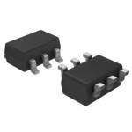
| 描述 | IC CHANNEL PROTECTOR SGL SOT23-6模拟开关 IC SGL CH PROTECTOR IC |
| 产品分类 | |
| 品牌 | Analog Devices |
| 产品手册 | |
| 产品图片 |
|
| rohs | 符合RoHS无铅 / 符合限制有害物质指令(RoHS)规范要求 |
| 产品系列 | 开关 IC,模拟开关 IC,Analog Devices ADG465BRTZ-REEL7- |
| 数据手册 | |
| 产品型号 | ADG465BRTZ-REEL7 |
| PCN过时产品 | |
| 产品目录页面 | |
| 产品种类 | 模拟开关 IC |
| 供应商器件封装 | SOT-23-6 |
| 其它名称 | ADG465BRTZ-REEL7CT |
| 功率(W) | - |
| 包装 | Digi-Reel® |
| 商标 | Analog Devices |
| 安装风格 | SMD/SMT |
| 封装 | Reel |
| 封装/外壳 | SOT-23-6 |
| 封装/箱体 | SOT-23-6 |
| 工作电源电压 | 20 V |
| 工厂包装数量 | 3000 |
| 应用 | 通用 |
| 开关数量 | 1 |
| 开关电压—最大值 | 20 V |
| 技术 | 混合技术 |
| 最大功率耗散 | 15 uW |
| 最大工作温度 | + 85 C |
| 最小工作温度 | - 40 C |
| 标准包装 | 1 |
| 电压-工作 | - |
| 电压-箝位 | ±40V |
| 电源电压-最大 | 20 V |
| 电源电压-最小 | 20 V |
| 电源电流—最大值 | 500 nA |
| 电路数 | 1 |
| 系列 | ADG465 |


PDF Datasheet 数据手册内容提取
Single Channel Protector in a SOT-23 Package and a MSOP Package Data Sheet ADG465 FEATURES FUNCTIONAL BLOCK DIAGRAM Fault and overvoltage protection up to ±40 V VDD VSS Signal paths open circuit with power off Signal path resistance of RON with power on VIN VD1 VS1 VOUT Supply maximum ratings (VDD to VSS): 44 V VIN ADG465 VOUT Low on resistance (R ): 80 Ω typical ON ±1 nA maximum path current leakage at 25°C VDD VDD Low power dissipation: 0.8 µW typical Latch-up proof construction APPLICATIONS OATU TVPDUD T– C1L.5AVMPED 09538-001 ATE equipment Figure 1. Sensitive measurement equipment Hot insertion rack systems ADC input channel protection GENERAL DESCRIPTION The ADG465 is a single channel protector that comes in SOT-23 The ADG465 can operate from both bipolar and unipolar supplies. and MSOP packages. The channel protector is in series with the The channels are normally on when power is connected, and signal path and protects sensitive components from voltage open circuit when power is disconnected. With power supplies of transience in the signal path whether or not the power supplies ±15 V, the on resistance of the ADG465 is 80 Ω typical, with a are present. Because the channel protection works regardless of leakage current of ±1 nA maximum. When power is disconnected, the presence of the supplies, the channel protectors are ideal for the input leakage current is approximately ±0.005 µA typical. use in applications where correct power sequencing cannot The ADG465 is available in a 6-lead SOT-23 package, and an always be guaranteed to protect the analog inputs (for example, hot 8-lead MSOP package. insertion rack systems). See the Applications Information section PRODUCT HIGHLIGHTS for further details. 1. Fault Protection. A channel protector consists of an N channel, metal-oxide The ADG465 can withstand continuous voltage inputs from semiconductor field-effect transistor (MOSFET), a P channel −40 V to +40 V. When a fault occurs due to the power supplies MOSFET, and another N channel MOSFET connected in series. being turned off, or due to an overvoltage being applied to The channel protector behaves like a series resistor during normal the ADG465, the output is clamped. When power is turned operation, that is, (V + 1.5 V) < V < (V − 1.5 V). When the SS IN DD off, current is limited to the nanoampere level. analog input of a channel exceeds the power supplies (including 2. Low Power Dissipation. V and V = 0 V), one of the MOSFETs switches off, clamping DD SS 3. Low R 80 Ω typical. the output to either V + 1.5 V or V − 1.5 V. Circuitry and ON SS DD 4. Trench Isolation Latch-Up Proof Construction. signal source protection are provided in the event of an overvoltage A dielectric trench separates the P channel and the or power loss. The channel protectors can withstand overvoltage N channel MOSFETs thereby preventing latch up. inputs from −40 V to +40 V. See the Theory of Operation section for further details. Rev. C Document Feedback Information furnished by Analog Devices is believed to be accurate and reliable. However, no responsibility is assumed by Analog Devices for its use, nor for any infringements of patents or other One Technology Way, P.O. Box 9106, Norwood, MA 02062-9106, U.S.A. rights of third parties that may result from its use. Specifications subject to change without notice. No license is granted by implication or otherwise under any patent or patent rights of Analog Devices. Tel: 781.329.4700 ©1997–2018 Analog Devices, Inc. All rights reserved. Trademarks and registered trademarks are the property of their respective owners. Technical Support www.analog.com
ADG465 Data Sheet TABLE OF CONTENTS Features .............................................................................................. 1 Typical Performance Characteristics ..............................................6 Applications ....................................................................................... 1 Test Circuits ........................................................................................8 Functional Block Diagram .............................................................. 1 Theory of Operation .........................................................................9 General Description ......................................................................... 1 Overvoltage Protection .................................................................9 Product Highlights ........................................................................... 1 Trench Isolation .......................................................................... 10 Revision History ............................................................................... 2 Applications Information .............................................................. 11 Specifications ..................................................................................... 3 Overvoltage and Power Supply Sequencing Protection ............ 11 Dual Supply ................................................................................... 3 High Voltage Surge Suppression .............................................. 11 Absolute Maximum Ratings ............................................................ 4 Outline Dimensions ....................................................................... 12 Thermal Resistance ...................................................................... 4 Ordering Guide .......................................................................... 12 ESD Caution .................................................................................. 4 Pin Configurations and Function Descriptions ........................... 5 REVISION HISTORY 8/2018—Rev. B to Rev. C Added Figure 10 ................................................................................ 7 Changes to V, V , Analog Input Overvoltage with Power Off Added Test Circuits Section and Figure 11 to Figure 13 .............. 8 S D Parameter, Table 2 ............................................................................. 4 Changed Circuit Information Section to Theory of Operation Change to High Voltage Surge Suppression Section ................. 11 Section .................................................................................................9 Changes to Figure 16 ......................................................................... 9 12/2017—Rev. A to Rev. B Changes to Overvoltage Protection ............................................. 10 Updated Format .................................................................. Universal Changes to Overvoltage and Power Supply Sequencing Protection Changes to Product Title and General Description Section ....... 1 Section .............................................................................................. 11 Changes to Table 1 ............................................................................ 3 Updated Outline Dimensions ....................................................... 12 Added Thermal Resistance Section and Table 3; Renumbered Changes to Ordering Guide .......................................................... 12 Sequentially ....................................................................................... 4 Changes to Figure 2, Figure 3, and Table 4 ................................... 5 1/1997—Revision 0: Initial Version Changes to Figure 4 to Figure 8 ...................................................... 6 Added Figure 9; Renumbered Sequentially .................................. 6 Rev. C | Page 2 of 12
Data Sheet ADG465 SPECIFICATIONS DUAL SUPPLY V = +15 V, V = −15 V, GND = 0 V, unless otherwise noted. DD SS Table 1. 25°C −40°C to +85°C Parameter Symbols Min Typ Max Min Typ Max Unit Test Conditions/Comments FAULT PROTECTED CHANNEL Fault Free Analog Signal Range1 V + V – V Output open circuit SS DD 1.5 1.5 On Resistance R 80 99.5 126.5 Ω −10 V ≤ V2 ≤ +10 V, I = 1 mA ON S S RON Flatness 8.5 9 Ω −5 V ≤ VS2 ≤ +5 V LEAKAGE CURRENTS Channel Output Leakage I ±0.1 ±1 ±1 ±5 nA V2 = V 2 = ±10 V S (ON) S D (Without Fault Condition) Channel Input Leakage (With I ±0.2 ±2 ±0.4 ±5 nA V2 = ±25 V, V 2 = open circuit D (ON) S D Fault Condition) Channel Input Leakage (With I ±0.5 ±2 ±2 ±10 nA V = 0 V, V = 0 V, V2 = ±35 V, D (OFF) DD SS S Power Off and Fault) V 2 = open circuit D Channel Input Leakage (With I ±0.005 ±0.015 ±0.1 ±0.5 µA V = 0 V, V = 0 V, V2 = ±35 V, D (OFF) DD SS S Power Off and Output Short V 2 = 0 V D Circuit) POWER REQUIREMENTS Positive Supply Current I ±0.05 ±0.5 ±5 µA DD Negative Supply Current I ±0.05 ±0.5 ±5 µA SS Positive/Negative Power Supply V /V 0 ±20 0 ±20 V DD SS 1 Guaranteed by design, not subject to production test. 2 VS is the voltage at the source of the switch and VD is the voltage at the drain of the switch. Rev. C | Page 3 of 12
ADG465 Data Sheet ABSOLUTE MAXIMUM RATINGS THERMAL RESISTANCE T = 25°C, unless otherwise noted. A θ is specified for the worst-case conditions, that is, a device JA Table 2. soldered in a circuit board for surface-mount packages. Parameter Rating V to V 44 V Table 3. Thermal Resistance DD SS VS, VD, Analog Input Overvoltage with VSS – 20 V to VDD + 20 V Package Type θJA θJC Unit Power On1 6-Lead SOT-231 230 92 °C/W VS, VD, Analog Input Overvoltage with −40 V to +40 V 8-Lead MSOP2 206 44 °C/W Power Off1 Continuous Current, S or D 20 mA 1 Thermal impedance simulated values are based on JEDEC 1S 2-layer test board. See EIA/JEDEC standard JESD51. Peak Current, S or D (Pulsed at 1 ms, 40 mA 2 Thermal impedance simulated values are based on JEDEC 2S2P 4-layer test 10% Duty Cycle Maximum) board. See EIA/JEDEC standard JESD51. Operating Temperature Range −40°C to +85°C Storage Temperature Range −65°C to +125°C ESD CAUTION Junction Temperature 150°C Lead Temperature, Soldering Vapor Phase (60 sec) 215°C Infrared (15 sec) 220°C 1 The channel protector clamps overvoltages at the source (S) or the drain (D) of the switch. See the Theory of Operation section for more information. Stresses at or above those listed under Absolute Maximum Ratings may cause permanent damage to the product. This is a stress rating only; functional operation of the product at these or any other conditions above those indicated in the operational section of this specification is not implied. Operation beyond the maximum operating conditions for extended periods may affect product reliability. Rev. C | Page 4 of 12
Data Sheet ADG465 PIN CONFIGURATIONS AND FUNCTION DESCRIPTIONS VD1 1 6 VDD NIC 1 8 NIC ADG465 VDD 2 ADG465 7 VD1 NIC 2 TOP VIEW 5 NIC TOP VIEW (Not to Scale) VS1 3 (Not to Scale) 6 VSS VSS 3 4 VS1 NIC 4 5 NIC N1.ONDTIOCE SN=O NTO CTO INNTNEERCNTA.LLY CONNECTED. 09538-002 N1.ONDTIOCE SN=O NTO CTO INNTNEERCNTA.LLY CONNECTED. 09538-003 Figure 2. 6-Lead SOT-23 Pin Configuration Figure 3. 8-Lead MSOP Pin Configuration Table 4. Pin Function Descriptions Pin No. 6-Lead SOT-23 8-Lead MSOP Mnemonic Description 1 7 V One Terminal of the Channel Protector. The channel protector is bidirectional so this D1 terminal can be used as an input or an output. 2, 5 1, 4, 5, 8 NIC Not Internally Connected. Do not connect. 3 6 V Negative Power Supply (0 V to −20 V). The clamping point for a negative overvoltage is SS also defined as V . See the Overvoltage Protection section. SS 4 3 V One Terminal of the Channel Protector. The channel protector is bidirectional so this S1 terminal can be used as an input or an output. 6 2 V Positive Power Supply (0 V to 20 V). The clamping point for a positive overvoltage is also DD defined as V . See the Overvoltage Protection section. DD Rev. C | Page 5 of 12
ADG465 Data Sheet TYPICAL PERFORMANCE CHARACTERISTICS 150 30 POSITIVE OVERVOLTAGE ON INPUT 140 RLOAD = 100kΩ 130 25 CVDLOD A=D + =1 01V00pF 120 20 VSS = –10V –5V TO +15V STEP INPUT 110 VDD = +5V V) 15 Ω) 100 VSS = –5V E ( (N 90 AG 10 O T R L 80 VDD = +10V VO 5 70 VSS = –10V CHANNEL PROTECTOR OUTPUT 60 0 50 –5 40 VDD = +16.5V VSS = –16.5V TA = 25°C 30–10 –5 VS0 (V) 5 10 09538-004 –100 50 100 150 200TIM2E5 0(ns)300 350 400 450 500 09538-006 Figure 4. On Resistance (RON) vs. Input Voltage (VS) as a Function of VDD/VSS Figure 7. Positive Overvoltage Transience Response 130 VDD = +15V 10 120 VSS = –15V 5 110 0 100 CHANNEL PROTECTOR V) –5 OUTPUT Ω) 90 E ( R (ON 80 TA = 125°C LTAG –10 O V –15 70 TA = 80°C NEGATIVE OVERVOLTAGE 60 –20 ON INPUT +S5TVE PTO IN –P1U5TV TA = 25°C RLOAD = 100kΩ 50 –25 CLOAD = 100pF VDD = +10V 40–10 –5 VS0 (V) 5 10 09538-005 –300VSS 5=0 –101V00 150 200TIM2E5 0(ns)300 350 400 450 500 09538-007 Figure 5. On Resistance (RON) vs. Input Voltage (VS) as a Function of Figure 8. Negative Overvoltage Transience Response Temperature 15 0 VDD = +15V –10V TO +10V INPUT –1 VSS = –15V 10 –2 TA = 25°C INPUT = 0dBm VCLAMP = +4.5V –3 5 dB) –4 GE (V) OUTPUT OSS ( ––65 TA 0 N L –7 L O VO RTI –8 –5 E –9 S VCLAMP = –4.1V IN –10 –11 –10 RLOAD = 100kΩ –12 VDD = +5V VSS = –5V –13 –150 100 200 300 400TIM5E0 0(ns)600 700 800 900 1000 09538-020 –14100 1k 10k FR1E0Q0kUENCY1M (Hz) 10M 100M 1G 09538-021 Figure 6. Overvoltage Ramp Figure 9. Frequency Response (Magnitude) Rev. C | Page 6 of 12
Data Sheet ADG465 0 VDD = +15V –10 VSS = –15V V p-p = 0.62V –20 TA = 25°C –30 dB) –40 NOC ADPEACCOIUTOPLRISNG R ( R –50 S P AC –60 –70 DECOUPLING CAPACITORS –80 ON SUPPLIES –90 –100100 1k F1R0EkQUENCY1 (0H0zk) 1M 10M 09538-022 Figure 10. AC Power Supply Rejection Ratio (ACPSRR) vs. Frequency, ±15 V Dual Supply Rev. C | Page 7 of 12
ADG465 Data Sheet TEST CIRCUITS IDS VDD VSS 0.1µF 0.1µF V1 NETWORK VDD VSS ANALYZER S D S 50Ω IN VS RON = V1/IDS VS D VIN RL VOUT N1.O DIDTRSEA SISIN T THOE TCHUER SRWENITTC FHR SOOMU TRHCEE .SWITCH 09538-023 50Ω INSERTION LOSS = 20 logVOVUOTUWTIWTHITOHU STW SIWTCITHCH 09538-025 Figure 11. On Resistance Figure 13. Bandwidth ID (ON) S D NC A NIC = NOT INTERNALLY CONNECTEVDD. 09538-024 Figure 12. On Leakage Rev. C | Page 8 of 12
Data Sheet ADG465 THEORY OF OPERATION Figure 14 shows a simplified schematic of a channel protector OVERVOLTAGE PROTECTION circuit. The circuit is comprised of four metal-oxide semiconductor When a fault condition occurs on the input of a channel protector, (MOS) transistors: two negative metal-oxide semiconductor the voltage on the input exceeds some threshold voltage set by (NMOS) and two positive metal-oxide semiconductor (PMOS). the supply rail voltages. The threshold voltages (V and V ) TP TN One of the PMOS devices does not lie directly in the signal path; are related to the supply rails. For a positive overvoltage, the however, it connects the source of the second PMOS device to threshold voltage is given by V − V , where V is the threshold DD TN TN its back gate, which has the effect of lowering the threshold voltage voltage of the NMOS transistor (1.5 V typical). For a negative and increasing the input signal range of the channel for normal overvoltage, the threshold voltage is given by V − V , where SS TP operation. The source and back gate of the NMOS devices are V is the threshold voltage of the PMOS device (1.5 V typical). TP connected for the same reason. During normal operation, the If the input voltage exceeds these threshold voltages, the output channel protectors have a resistance of 80 Ω typical. The channel of the channel protector (with no load) is clamped at these protectors are low power devices; even under fault conditions, threshold voltages. However, the channel protector output the supply current is limited to submicroampere levels. All clamps at a voltage inside these thresholds if the output is loaded. transistors are dielectrically isolated from each other using For example, with an output load of 1 kΩ, V = 15 V and a DD trench isolation. Using trench isolation makes it impossible to positive overvoltage. The output clamps at V − V − ΔV = 15 DD TN latch up the channel protectors. For further details, see the V − 1.5 V − 0.6 V = 12.9 V, where ΔV is due to IR voltage drops Trench Isolation section. across the channels of the MOS devices (see Figure 16). As shown in Figure 16, the current during fault condition is determined by the load on the output (that is, V /R). VSS CLAMP L However, if the supplies are off, the fault current is limited to the nanoampere level. PMOS NMOS NMOS Figure 15, Figure 18, and Figure 19 show the operating conditions of the signal path transistors during various fault VDD VSSPMOS VDD 09538-010 cwohnedni taio pnoss. iFtiivgeu orev e1r5v sohltoawges ihso awp ptlhieed c htoa nthnee lc phraontnecetl oprrso otepcetroart.e Figure 14. Channel Protector Circuit Schematic The first NMOS transistor goes into a saturated mode of operation as the voltage on its drain exceeds the gate voltage (V ) − the threshold voltage, V (see Figure 16). The potential DD TN at the source of the NMOS device is equal to V − V . The DD TN other MOS devices are in a nonsaturated mode of operation. VDD – VTN* (+13.5V) POSITIVE NMOS PMOS NMOS OVERVOLTAGE (+20V) SATURATED NONSATURATED NONSATURATED *VTN = NMOS THRESHVODLDD ( +V1O5LVT)AGE (+1.5VV)SS (–15V) VDD (+15V) 09538-011 Figure 15. Positive Overvoltage on the Channel Protector VD VG VS ΔV (+13.5V) (+20V) (VDD = +15V) PMOS NMOS N+ N+ N+ NONSATURATED OVOEPREVROALTTIOANGE SPEAFCFEE CCHTAIVREGE N-CHANNEL OPERATION RL VCLAMP (SATURATED) REGION IOUT VT = 1.5V P– (VG – VT = 13.5V) N1.OVGTDAE TISSE TOHFE T VHOEL STWAGITEC AHT, ATNHDE VDSR IASI NT HOEF V TOHLET SAWGEIT CAHT ,T VHGE I SS OTHUER CVEO LOTFA TGHEE A STW TIHTCEH. 09538-012 Figure 16. Negative Overvoltage Operation on the Channel Protector Rev. C | Page 9 of 12
ADG465 Data Sheet When a negative overvoltage is applied to the channel protector (CMOS) transistors. Latch up is caused when PN junctions that circuit, the PMOS transistor enters a saturated mode of operation are normally reverse biased become forward biased, causing as the drain voltage exceeds V − V (see Figure 18). As in the large currents to flow, which can be destructive. SS TP case of the positive overvoltage, the other MOS devices are in a CMOS devices are normally isolated from each other by junction nonsaturated mode of operation. isolation. In junction isolation, the N and P wells of the CMOS The channel protector is also functional when the supply transistors form a diode that is reverse biased under normal rails are down (for example, power failure) or momentarily operation. However, during overvoltage conditions, this diode unconnected (for example, rack system). The channel protector is becomes forward biased. Two transistors form a silicon-controlled in the off high impedance state with no supply rail voltage applied, rectifier (SCR) type circuit, causing a significant amplification this known power supply state is where the channel protector has of the current that, in turn, leads to latch up. With trench isolation, an advantage over more conventional protection methods, such this diode is removed, resulting in a latch-up proof circuit. as diode clamping (see the Applications Information section). VG VG When V and V equal 0 V, all transistors are off, and the VS VD VS VD DD SS current is limited to microampere levels (see Figure 19). TRENCH ISOLATION RT P+ P-CHANNEL P+ RT N+ N-CHANNEL N+ RT E E E N N N The MOS devices that make up the channel protector are isolated CH N– CH P– CH from each other by an oxide layer (trench, see Figure 17). When BURIED OXIDE LAYER tehaec hN oMthOerS, athnedr eP iMs aO lSa tdcehv-iucpe sp aorses inboilti teyl eccaturisceadl lbyy i spoalaratesdit ifcr om SUBSTRATE (BACKGATE) 09538-015 Figure 17. Trench Isolation junctions between complementary metal-oxide semiconductor NEGATIVE VSS – VTP* OVERVOLTAGE (–13V) (–20V) NEGATIVE NMOS PMOS NMOS OVERVOLTAGE (–20V) NONSATURATED SATURATED NONSATURATED *VTP = PMOS THRESHVODLDD ( +V1O5LVT)AGE (+2V)VSS (–15V) VDD (+15V) 09538-013 Figure 18. Negative Overvoltage on the Channel Protector 0V POSITIVE OR NMOS PMOS NMOS NEGATIVE OVERVOLTAGE OFF OFF OFF VDD (0V) VSS (0V) VDD (0V) 09538-014 Figure 19. Channel Protector Supplies Equal to 0 V Rev. C | Page 10 of 12
Data Sheet ADG465 APPLICATIONS INFORMATION OVERVOLTAGE AND POWER SUPPLY SEQUENCING HIGH VOLTAGE SURGE SUPPRESSION PROTECTION The ADG465 is not intended for use in high voltage applications, The ADG465 is ideal for use in applications where input such as surge suppression. The ADG465 has breakdown voltages overvoltage protection is required and correct power supply of V − 20 V and V + 20 V on the inputs when the power SS DD sequencing cannot always be guaranteed. The overvoltage supplies are connected. When the power supplies are disconnected, protection ensures that the output voltage of the channel protector the breakdown voltages on the input of the channel protector does not exceed the threshold voltages set by the supplies (see are ±40 V. In applications where inputs are likely to be subject the Theory of Operation section) when there is an overvoltage to overvoltages exceeding the breakdown voltages quoted for on the input. When the input voltage does not exceed these the channel protectors, use transient voltage suppressors (TVSs). threshold voltages, the channel protector behaves like a series These devices protect vulnerable circuits from electric overstress resistor (80 Ω typical). The resistance of the channel protector such as that caused by electrostatic discharge, inductive load does vary slightly with operating conditions (see the Typical switching, and induced lightning. However, TVSs can have a Performance Characteristics section). substantial standby (leakage) current (300 µA typical) at the When a voltage is not applied to V and V , the channel protector reverse standoff voltage. The reverse standoff voltage of a TVS DD SS is in an off state and presents high impedance, which is particularly is the normal peak operating voltage of the circuit. In addition, useful when considering power sequencing and protection of TVSs offer no protection against latch up of sensitive CMOS downstream circuitry during a system power up. When there is devices when the power supplies are off. To provide the best no voltage applied to the supply rails, all transistors in the channel leakage current specification and circuit protection, the best protector are off, and the only currents that flow are leakage solution is to use a channel protector in conjunction with a TVS. currents, which are at the microampere levels. Figure 21 shows an input protection scheme that uses both a TVS Figure 20 shows a typical application requiring overvoltage and and channel protector. The TVS is selected with a reverse standoff power supply sequencing protection. The application shows a voltage much greater than the operating voltage of the circuit hot insertion rack system that involves plugging a circuit board (TVSs with higher breakdown voltages tend to have better or module into a live rack via an edge connector. In this type of standby leakage current specifications); however, inside the application, it is not possible to guarantee correct power supply breakdown voltage of the channel protector. This circuit protects sequencing. Power supplies must be connected prior to any the circuitry whether or not the power supplies are present. external signals for correct power supply sequencing. Incorrect VDD = +5V VSS = –5V power sequencing can cause a CMOS device to latch up, which is true of most CMOS devices, regardless of the functionality (see the Trench Isolation section). Use RC networks on the supplies ADG465 of the channel protector (see Figure 20) to ensure that the rest of ADC the circuitry is powered up before the channel protectors. The outputs of the channel protectors are clamped well below V and DD V until the capacitors are charged. The diodes ensure that the SS TVSs supplies on the channel protectors never exceed the supply rails BREAKDOWN oonf tthhee binopaurdts wofh tehne iCt Mis OdiSs cdoenvniceecst nedev, earn edx ceenesdu rteh eth sautp apnliye ssi. gnals VOLTAGE = 20V 09538-017 Figure 21. High Voltage Protection EDGE CONNECTOR VDD +5V VSS –5V –2.5AVN TAOL O+G2. 5INV ADC ADG465 LOGIC CONTROL LOGIC LOGIC GND 09538-016 Figure 20. Overvoltage and Power Supply Sequencing Protection Rev. C | Page 11 of 12
ADG465 Data Sheet OUTLINE DIMENSIONS 3.00 2.90 2.80 1.70 6 5 4 3.00 1.60 2.80 1.50 2.60 1 2 3 PIN1 INDICATOR 0.95BSC 1.90 BSC 1.30 1.15 0.90 1.45MAX 0.20MAX 0.95MIN 0.08MIN 0.55 0.15MAX 10° 0.45 0.05MIN 0.50MAX SPELAATNIENG 4° B0S.6C0 0.35 0.30MIN 0° COMPLIANTTOJEDECSTANDARDSMO-178-AB 12-16-2008-A Figure 22. 6-Lead Small Outline Transistor Package [SOT-23] (RJ-6) Dimensions shown in millimeters 3.20 3.00 2.80 8 5 5.15 3.20 4.90 3.00 4.65 2.80 1 4 PIN 1 IDENTIFIER 0.65 BSC 0.95 15° MAX 0.85 1.10 MAX 0.75 0.80 0.15 0.40 6° 0.23 0.55 CO0P.0L50A.1N0ARICTOYMPLIANT0. 2T5O JEDEC STA0°NDARDS 0M.0O9-187-AA 0.40 10-07-2009-B Figure 23. 8-Lead Mini Small Outline Package [MSOP] (RM-8) Dimensions shown in millimeters ORDERING GUIDE Model1 Temperature Range Package Description Marking Code Package Option ADG465BRTZ-REEL7 −40°C to +85°C 6-Lead Small Outline Transistor Package [SOT-23], Reel S1E RJ-6 ADG465BRMZ −40°C to +85°C 8-Lead Mini Small Outline Package [MSOP], Reel S1E RM-8 1 Z = RoHS Compliant Part. ©1997–2018 Analog Devices, Inc. All rights reserved. Trademarks and registered trademarks are the property of their respective owners. D09538-0-8/18(C) Rev. C | Page 12 of 12