ICGOO在线商城 > 电路保护 > TVS - 混合技术 > FR014H5JZ
 Datasheet下载
- 型号: FR014H5JZ
- 制造商: Fairchild Semiconductor
- 库位|库存: xxxx|xxxx
- 要求:
| 数量阶梯 | 香港交货 | 国内含税 |
| +xxxx | $xxxx | ¥xxxx |
查看当月历史价格
查看今年历史价格
FR014H5JZ产品简介:
ICGOO电子元器件商城为您提供FR014H5JZ由Fairchild Semiconductor设计生产,在icgoo商城现货销售,并且可以通过原厂、代理商等渠道进行代购。 FR014H5JZ价格参考。Fairchild SemiconductorFR014H5JZ封装/规格:TVS - 混合技术, 。您可以下载FR014H5JZ参考资料、Datasheet数据手册功能说明书,资料中有FR014H5JZ 详细功能的应用电路图电压和使用方法及教程。
ON Semiconductor的FR014H5JZ是一款采用混合技术的瞬态电压抑制器(TVS),属于TVS二极管中的混合型保护器件。该器件结合了雪崩二极管和晶闸管技术的优点,具备快速响应、高浪涌承受能力和低钳位电压等特性。

FR014H5JZ主要应用于需要高效、可靠静电放电(ESD)和瞬态过压保护的电子系统中。典型应用场景包括:便携式消费类电子产品(如智能手机、平板电脑、可穿戴设备)、USB接口保护(尤其是USB 2.0和USB 3.0高速数据线)、HDMI端口、音频/视频接口以及各类通信端口的信号线保护。其低电容设计确保对高速信号传输的影响最小,适合高频信号线路的防护。

此外,该器件也适用于工业控制设备、汽车电子中的非动力总成模块(如车载信息娱乐系统、传感器接口)等对电磁兼容性和可靠性要求较高的环境。FR014H5JZ采用SOD-323小型封装,节省PCB空间,适合高密度布局的现代电子设备。

总体而言,FR014H5JZ凭借其优异的瞬态抑制能力、紧凑尺寸和高可靠性,广泛用于各类电子产品的接口级过压保护,有效提升系统抗干扰能力和使用寿命。
| 参数 | 数值 |
| 产品目录 | |
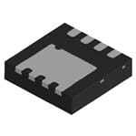
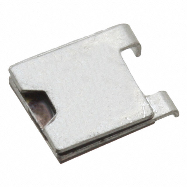
| 描述 | HI SIDE REV BIAS PROTECT 30V MLPTVS 二极管 - 瞬态电压抑制器 High-Side Reverse Bias Protector |
| 产品分类 | |
| 品牌 | Fairchild Semiconductor |
| 产品手册 | |
| 产品图片 |
|
| rohs | 符合RoHS无铅 / 符合限制有害物质指令(RoHS)规范要求 |
| 产品系列 | 二极管与整流器,TVS二极管,TVS 二极管 - 瞬态电压抑制器,Fairchild Semiconductor FR014H5JZ- |
| 数据手册 | |
| 产品型号 | FR014H5JZ |
| 产品种类 | TVS 二极管 - 瞬态电压抑制器 |
| 供应商器件封装 | 8-MLP(3.3x3.3) |
| 其它名称 | FR014H5JZDKR |
| 击穿电压 | 31.2 V |
| 功率(W) | - |
| 包装 | Digi-Reel® |
| 单位重量 | 200 mg |
| 商标 | Fairchild Semiconductor |
| 安装风格 | SMD/SMT |
| 封装 | Reel |
| 封装/外壳 | 8-WDFN 裸露焊盘 |
| 封装/箱体 | MLP-6 |
| 尺寸 | 2.1 mm W x 2.32 mm L x 0.8 mm H |
| 峰值脉冲功率耗散 | 36 W |
| 工作电压 | 25 V |
| 工厂包装数量 | 3000 |
| 应用 | 反极性,过压保护 |
| 技术 | 混合技术 |
| 最大工作温度 | + 150 C |
| 最小工作温度 | 0 C |
| 极性 | Unidirectional |
| 标准包装 | 1 |
| 电压-工作 | 30V |
| 电压-箝位 | 34V |
| 电路数 | 1 |
| 端接类型 | SMD/SMT |
| 系列 | FR014H5JZ |
| 钳位电压 | 34 V |


- 商务部:美国ITC正式对集成电路等产品启动337调查
- 曝三星4nm工艺存在良率问题 高通将骁龙8 Gen1或转产台积电
- 太阳诱电将投资9.5亿元在常州建新厂生产MLCC 预计2023年完工
- 英特尔发布欧洲新工厂建设计划 深化IDM 2.0 战略
- 台积电先进制程称霸业界 有大客户加持明年业绩稳了
- 达到5530亿美元!SIA预计今年全球半导体销售额将创下新高
- 英特尔拟将自动驾驶子公司Mobileye上市 估值或超500亿美元
- 三星加码芯片和SET,合并消费电子和移动部门,撤换高东真等 CEO
- 三星电子宣布重大人事变动 还合并消费电子和移动部门
- 海关总署:前11个月进口集成电路产品价值2.52万亿元 增长14.8%


PDF Datasheet 数据手册内容提取
Is Now Part of To learn more about ON Semiconductor, please visit our website at www.onsemi.com Please note: As part of the Fairchild Semiconductor integration, some of the Fairchild orderable part numbers will need to change in order to meet ON Semiconductor’s system requirements. Since the ON Semiconductor product management systems do not have the ability to manage part nomenclature that utilizes an underscore (_), the underscore (_) in the Fairchild part numbers will be changed to a dash (-). This document may contain device numbers with an underscore (_). Please check the ON Semiconductor website to verify the updated device numbers. The most current and up-to-date ordering information can be found at www.onsemi.com. Please email any questions regarding the system integration to Fairchild_questions@onsemi.com. ON Semiconductor and the ON Semiconductor logo are trademarks of Semiconductor Components Industries, LLC dba ON Semiconductor or its subsidiaries in the United States and/or other countries. ON Semiconductor owns the rights to a number of patents, trademarks, copyrights, trade secrets, and other intellectual property. A listing of ON Semiconductor’s product/patent coverage may be accessed at www.onsemi.com/site/pdf/Patent-Marking.pdf. ON Semiconductor reserves the right to make changes without further notice to any products herein. ON Semiconductor makes no warranty, representation or guarantee regarding the suitability of its products for any particular purpose, nor does ON Semiconductor assume any liability arising out of the application or use of any product or circuit, and specifically disclaims any and all liability, including without limitation special, consequential or incidental damages. Buyer is responsible for its products and applications using ON Semiconductor products, including compliance with all laws, regulations and safety requirements or standards, regardless of any support or applications information provided by ON Semiconductor. “Typical” parameters which may be provided in ON Semiconductor data sheets and/or specifications can and do vary in different applications and actual performance may vary over time. All operating parameters, including “Typicals” must be validated for each customer application by customer’s technical experts. ON Semiconductor does not convey any license under its patent rights nor the rights of others. ON Semiconductor products are not designed, intended, or authorized for use as a critical component in life support systems or any FDA Class 3 medical devices or medical devices with a same or similar classification in a foreign jurisdiction or any devices intended for implantation in the human body. Should Buyer purchase or use ON Semiconductor products for any such unintended or unauthorized application, Buyer shall indemnify and hold ON Semiconductor and its officers, employees, subsidiaries, affiliates, and distributors harmless against all claims, costs, damages, and expenses, and reasonable attorney fees arising out of, directly or indirectly, any claim of personal injury or death associated with such unintended or unauthorized use, even if such claim alleges that ON Semiconductor was negligent regarding the design or manufacture of the part. ON Semiconductor is an Equal Opportunity/Affirmative Action Employer. This literature is subject to all applicable copyright laws and is not for resale in any manner.
F R 0 1 4 November 2012 H 5 J Z — H i g FR014H5JZ (14mΩ, -30V) h S High-Side Reverse Bias / Reverse Polarity Protector i d e With Integrated Over Voltage Transient Suppression R e v e r s Features e Description B Up to -30V Reverse-Bias Protection ia Reverse bias is an increasingly common fault event that s Nano Seconds of Reverse-Bias Blocking may be generated by user error, improperly installed / Response Time batteries, automotive environments, erroneous R e +32V 24-Hour “Withstand” Rating ctroannnseiecntitosn, si ntod utchtiirvde- patrratyn sciehnatrsg,e rasn, dn ergeaatdiviley “haovta iplalubgle” ve r 14mΩ Typical Series Resistance at 5V negatively biased rouge USB chargers. s e Integrated TVS Over Voltage Suppression Fairchild circuit protection is proud to offer a new type of P reverse bias protection devices. The FR devices are low o MLP 3.3x3.3 Package Size resistance, series switches that, in the event of a la r RoHs Compliant reverse bias condition, shut off power and block the it y USB Tested and Compatible negative voltage to help protect downstream circuits. P The FR devices are optimized for the application to offer ro best in class reverse bias protection and voltage t Applications e capabilities while minimizing size, series voltage drop, c t USB 1.0, 2.0 and 3.0 Devices and normal operating power consumption. o r USB Charging In the event of a reverse bias application, FR014H5JZ W devices effectively provide a full voltage block and can i Mobile Devices easily protect -0.3V rated silicon. th I Mobile Medical From a power perspective, in normal bias, a 14mΩ FR nt e POS Systems device in a 1.5A application will generate only 21mV of g voltage drop or 32mW of power loss. In reverse bias, r Toys FR devices dissipate less then 20µW in a 16V reverse at e Any DC Barrel Jack Powered Device bias event. This type of performance is not possible with d a diode solution. O Any DC Devices subject to Negative Hot Plug or v Inductive Transients Benefits extend beyond the device. Due to low power e r dissipation, not only is the device small, but heat sinking Automotive Peripherals requirements and cost can be minimized as well. Vo l ta g e T r a n s i e n t S Ordering Information u p p Part Number Top Mark Package Packing Method r e 8-Lead, Molded Leadless Package (MLP), 3000 on Tape & Reel; s FR014H5JZ 14H s Dual, 3.3mm Square 13-inch Reel, 12mm Tape io n © 2012 Fairchild Semiconductor Corporation www.fairchildsemi.com FR014H5JZ • Rev. C2
F R 0 1 Diagrams 4 H 5 OV Bypass FR014H5JZ J Protection POS NEG Z POS Inrush Reducer NEG IIN — Startup Diode CTL H Power Source USB Device Power (USB Connector) VIN Circuit ig h Switch S i d e CTL Protected USB Device Circuit R e v Figure 1. Block Diagram Figure 2. Typical Schematic e r s e B i a s Pin Configuration / R e v e r s e P o l a r i t y P r o t e c t o r W Figure 3. Pin Assignments i t h Pin Definitions I n t e Name Pin Description g r a POS 5, 6, 7, 8 The positive terminal of the power source. Current flows into this pin during normal te operation. d The control pin of the device. A negative voltage to the POS pin turns the switch on and a O CTL 4 positive voltage turns the switch to a high-impedance state. v e r The positive terminal of the load circuit to be protected. Current flows out of this pin during NEG 1, 2, 3 V normal operation. o l t a g e T r a n s i e n t S u p p r e s s i o n © 2012 Fairchild Semiconductor Corporation www.fairchildsemi.com FR014H5JZ • Rev. C2 2
F R 0 Absolute Maximum Ratings 1 4 H Values are at TA=25°C unless otherwise noted. 5 J Z Symbol Parameter Value Unit — Steady-State Normal Operating Voltage between POS and CTL Pins V+ +25 H MAX_OP (V = V+ , I = 1.5A, Switch On) IN MAX_OP IN i g 24-Hour Normal Operating Voltage Withstand Capability between POS h V+ 24 and CTL Pins (V = V+ , I = 1.5A, Switch On) (1) +32 V S IN 24 IN i d Steady-State Reverse Bias Standoff Voltage between POS and CTL Pins V- -30 e MAX_OP (V = V- ) IN MAX_OP R I Input Current V = 5V, Continuous(2) (see Figure 4) 8 A e IN IN v e TJ Operating Junction Temperature 150 °C r s T = 25°C 36 e PD Power Dissipation TAC = 25°C(2) (see Figure 4) 2.3 W Bia Steady-State Diode Continuous Forward Current from POS to NEG(2) s IDIODE_CONT (see Figure 4) 2 / R A I Pulsed Diode Forward Current from POS to NEG (300µs Pulse) (2) (see 450 ev DIODE_PULSE Figure 5) e r s Human Body Model, JESD22-A114 8 e P Charged Device Model, JESD22-C101 2 o Electrostatic NEG is shorted to CTL Contact 8 la ESD Discharge kV r Capability System Model, and connected to GND Air 15 ity IEC61000-4-2 No external connection Contact 3 P r between NEG and CTL Air 4 o t e Notes: c t 1. The V rating is NOT a survival guarantee. It is a statistically calculated survivability reference point taken on o +24 r qualification devices, where the predicted failure rate is less than 0.01% at the specified voltage for 24 hours. It is W intended to indicate the device’s ability to withstand transient events that exceed the recommended operating i voltage rating. Specification is based on qualification devices tested using accelerated destructive testing at th higher voltages, as well as production pulse testing at the V+24 level. Production device field life results may vary. In Results are also subject to variation based on implementation, environmental considerations, and circuit t e dynamics. Systems should never be designed with the intent to normally operate at V+24 levels. Contact Fairchild g Semiconductor for additional information. r a 2. The device power dissipation and thermal resistance (Rθ) are characterized with device mounted on the following te FR4 printed circuit boards, as shown in Figure 4 and Figure 5 d O ve r V o l t a g e T r a n s Figure 4. 1 Square Inch of 2-ounce copper Figure 5. Minimum Pads of 2-ounce Copper i e n t Thermal Characteristics S u p p Symbol Parameter Value Unit r e R Thermal Resistance, Junction to Case 3.4 s θJC °C/W s RθJA Thermal Resistance, Junction to Ambient(2) (see Figure 4) 50 io n © 2012 Fairchild Semiconductor Corporation www.fairchildsemi.com FR014H5JZ • Rev. C2 3
F R 0 1 Electrical Characteristics 4 H Values are at T = 25°C unless otherwise noted. 5 A J Z Symbol Parameter Conditions Min. Typ. Max. Unit — Positive Bias Characteristics H i V = +4V, I = 1.5A 18 23 g IN IN h VIN = +5V, IIN = 1.5A 14 19 S i RON Device Resistance, Switch On VIN = +5V, IIN = 1.5A, 20 mΩ de TJ = 125°C R V = +12V, I = 1.5A 11 14 e IN IN v Input Voltage, V , at which Voltage e IN r VON at POS, VPOS, Reaches a Certain IIN = 100mA, VPOS - VNEG = 2.0 2.4 3.0 V se Level at Given Current 50mV, VCTL = 0V B ∆VON / ∆TJ Temperature Coefficient of VON -3.52 mV/°C ia s V = V , I = 0.1A, VF Diode Forward Voltage PuCTlsLe widNEthG < D3IO0D0Eµs 0.57 0.63 0.70 V / R e Bias Current Flowing into POS Pin V = 5V, V = 0V, v IBIAS during Normal Bias Operation NPoO LSoad CTL 30 nA e r s Negative Bias Characteristics e P V- MAX_OP Reverse Bias Breakdown Voltage -30 V o ∆V- MAX_OP / Reverse Bias Breakdown Voltage IIN = -250µA, VCTL = VNEG =0V 22.5 mV/°C lar ∆T Temperature Coefficient i J t y I- Leakage Current from NEG to POS VPOS = -20V, 1 µA P in Reverse-Bias Condition VCTL = VNEG = 0V ro t V = 5V, V = 0V, C = e Time to Respond to Negative Bias CTL POS LOAD c tRN Condition 10µF, Reverse Bias Startup 50 ns to Inrush Current = 0.2A r W Integrated TVS Performance i t V Breakdown Voltage @ I I = 1mA, 300µs Pulse 28.5 30 31.2 V h Z T T I V = +25V, V = 0V 1.5 10 n NEG CTL I Leakage Current from NEG to CTL µA t R e VNEG = -25V, VCTL = 0V -1.5 -10 g r Max Pulse V > V 0.8 a NEG CTL t I Current from A e PPM NEG to CTL VNEG < VCTL -0.9 d IEC61000-4-5 O Clamping 8x20µs pulse VNEG > VCTL 34 v Voltage form e V V r C NEG to CTL at V < V -34 V NEG CTL I o PPM l t Dynamic Characteristics a g Input Capacitance between POS e C 2440 I and CTL T r a C Switch Capacitance between POS VIN = -5V, VCTL = VNEG = 0V, f 564 pF n S and NEG = 1MHz s i e Output Capacitance between NEG n CO and CTL 2526 t S R Control Internal Resistance 3.6 Ω u C p p r e s s i o n © 2012 Fairchild Semiconductor Corporation www.fairchildsemi.com FR014H5JZ • Rev. C2 4
F R 0 1 4 Typical Characteristics H 5 J TJ = 25°C unless otherwise specified. Z — G H Ωm) 24 NIN 3.6 ig CE ( 21 Input Voltage, VIN = 4V TUR 3.4 h S AN 18 GE V)3.2 id RESIST 1125 5V VOLTA WITCH (3.0 e Re R, SWITCH ON-ON 03690 2 4 9V6 12V8 161V0 12 14 16 18 20 V, MINIMUM INPUT ONON THE S2222....24680.0 0.3 0.6 0.9 1.2 1.5 1.8 2.1 verse Bias / I , INPUT CURRENT (A) I , INPUT CURRENT (A) R IN IN e v Figure 6. Switch On Resistance vs. Switch Current Figure 7. Minimum Input Voltage to Turn On Switch e r vs. Current at 50mV Switch Voltage Drop s e P Ω) o CE ( 1.0 Ω) 24 la CH RESISTAN 00..68 IIN0 =.9 0A.1A TJ = 25oC ESISTANCE (m 112581 IIN = 0.1A VIN = 5V rity Prote E SWIT 0.4 1.5A H ON-R 129 12V ctor TIV TC 6 W EC 0.2 WI i , EFFW 0.0 R, SON 03 th In RS 1 3 5 7 9 11 13 15 17 19 21 -75 -50 -25 0 25 50 75 100 125 150 t e V , INPUT VOLTAGE (V) T, JUNCTION TEMPERATURE (oC) g IN J r a t Figure 8. Effective Switch Resistance RSWvs. Figure 9. Switch On Resistance vs. Junction e Input Voltage V Temperature at 0.1A d IN O v e Ω) 24 1000 r V STANCE (m 112581 IIN = 1.5A VIN = 5V OWER (W) 100 oltage ESI E P T R 12 G 10 r N- A a H O 9 12V ACK ns WITC 6 AK P 1 ien ,SN 3 PE t S O R 0 0.1 u -75 -50 -25 0 25 50 75 100 125 150 1E-4 1E-3 0.01 0.1 1 10 100 1000 p p TJ, JUNCTION TEMPERATURE (oC) t, PULSE WIDTH (s) re s s Figure 10. Switch On Resistance vs.Junction Figure 11.Single-Pulse Maximum Power vs.Time i o Temperature at 1.5A n © 2012 Fairchild Semiconductor Corporation www.fairchildsemi.com FR014H5JZ • Rev. C2 5
F R 0 1 4 Typical Characteristics H 5 J TJ = 25°C unless otherwise specified. Z — A) H NT ( 100 ig RRE 10 VNEG = VCTL = 0V h S U ARD C 1 TJ = 125oC ide R W R 25oC e O v DE F 0.1 -55oC ers O P DI 0.01 e B U TART 1E-30.2 0.3 0.4 0.5 0.6 0.7 0.8 0.9 1.0 1.1 ias I, SF VF, STARTUP DIODE FORWARD VOLTAGE (V) / Re v Figure 12. Startup Diode Current vs. Forward Voltage e r s e P o l a r i t y P r o t e c t o r W i t h I n t e g r a t e d O v e r V o l t a g e T r a n s i e n t S u p p r e s s i o n © 2012 Fairchild Semiconductor Corporation www.fairchildsemi.com FR014H5JZ • Rev. C2 6
F R 0 Application Test Configurations 1 4 H FR014H5JZ 5 J Z POS NEG — I H IN i g CTL h Power Source USB Device S i V d (USB Connector) IN Circuit e R e v e r s e B i a Protected USB Device Circuit s / R Figure 13. Typical Application Circuit for USB Applications e v e rs e P FR014H5JZ o Q1-1 5,6 l a FDS8858CZ D2 POS NEG r i t y 3 S2 iIN P CTL ro 4 G2 t e R1 c t o r W D it SC Q1-2 h up P C1 7,8 D1 FDS8858CZ In po t lw e ye 2 G1 g r R3 C2 r a t e G d enP 1 S1 O eratoulse R2 ver V r o l t a g e T r a Figure 14. Startup Test Circuit – Normal Bias with FR014H5JZ n s i e n t S u p p r e s s i o n © 2012 Fairchild Semiconductor Corporation www.fairchildsemi.com FR014H5JZ • Rev. C2 7
F R 0 Application Test Configurations (Continued) 1 4 H FR014H5JZ 5 J POS NEG Z — iIN H G CTL i eneratoPulse R2 1 S1 gh Sid r e 2 G1 R Q1-2 e D v SC FDS8858CZ e up P 7,8 D1 rs po e lywe C1 R3 C2 B r i a s / R1 R 4 G2 e v e r 3 S2 5,6 D2 s e Q1-1 P FDS8858CZ o l a r Figure 15. Startup Test Circuit – Reverse Bias with FR014H5JZ it y P r o t e c Q1-1 to FDS8858CZ 5,6 D2 r W 3 S2 i iIN th I 4 G2 n t R1 e g r a t e D d SC Q1-2 O up P C1 7,8 D1 FDS8858CZ v po e lywe 2 G1 r V r R3 C2 o l t a G g eneratoPulse R2 1 S1 e Tran r s i e n t S u p Figure 16. Startup Test Circuit – without FR014H5JZ p r e s s i o n © 2012 Fairchild Semiconductor Corporation www.fairchildsemi.com FR014H5JZ • Rev. C2 8
F R 0 1 Typical Application Waveforms 4 H Typical USB3.0 conditions. 5 J Z — H i g h S i d ─ V , 2V/div. The input voltage between POS and CTL e IN ─ V , 2V/div. The output voltage between NEG and CTL R OUT e ─ VD, 1V/div. The startup diode voltage between POS and NEG v e ─ i , 5A/div. The input current flowing from POS to NEG IN r s e B i a s / R e v e r s e Time: 5µs/div P o l a ri t y Figure 17. Normal Bias Startup Waveform, DC Power Source=5V, C =100µF, C =10µF, R =R =10kΩ, R =27Ω 1 2 1 2 3 P ro t e c t o r W ─ V , 2V/div. The input voltage between POS and CTL IN i ─ VD, 2V/div. The startup diode voltage between POS and NEG th ─ V , 1V/div. The output voltage between NEG and CTL I OUT n ─ i , 0.1A/div. The input current flowing into POS t IN e g r a t e d O v e r V o l t a g e T r a n s i e n Time: 100ns/div t S u Figure 18. Reverse Bias Startup Waveform, DC Power Source=5V, C =100µF, C =10µF, R =R =10kΩ, R =27Ω 1 2 1 2 3 p p r e s s i o n © 2012 Fairchild Semiconductor Corporation www.fairchildsemi.com FR014H5JZ • Rev. C2 9
F R 0 1 Typical Application Waveforms (Continued) 4 H Typical USB3.0 conditions. 5 J Z — H i g h S i d e R e v e r s e B i a s ─ VIN, 2V/div. The voltage applied on the load circuit / ─ i , 2A/div. The input current R IN e v e r s e P o l a r Time: 5μs/div it y P Figure 19. Startup Waveform without FR014H5JZ, DC Power Source=5V, C1=100µF, C2=10uF, ro R1=R2=10kΩ, R3=27Ω t e c t Application Information o r W Figure 17 shows the voltage and current waveforms USB3.0 device is reversely biased; the output voltage is when a virtual USB3.0 device is connected to a 5V near 0 and response time is less than 50ns. it h source. A USB application allows a maximum source output capacitance of C = 120µF and a maximum Figure 19 shows the voltage and current waveforms In 1 when no reverse bias protection is implemented. In t device-side input capacitance of C = 10µF plus a e 2 Figure 17, while the reverse bias protector is present, g maximum load (minimum resistance) of R = 27Ω. C = 100µF, C = 10µF and R = 27Ω were used3 for testing1. the input voltage, VIN, and the output voltage, VO, are ra 2 3 separated and look different. When this reverse bias te When the DC power source is connected to the circuit protector is removed, V and V merge, as shown in d IN O (refer to Figure 13), the built-in startup diode initially Figure 19 as V . This V is also the voltage applied to O IN IN conducts the current such that the USB device powers the load circuit. It can be seen that, with reverse bias v e up. Due to the initial diode voltage drop, the FR014H5JZ protection, the voltage applied to the load and the r effectively reduces the peak inrush current of a hot plug current flowing into the load look very much the same as V o event. Under these test conditions, the input inrush without reverse bias protection. l t current reaches about 6A peak. While the current flows, a Benefits of Reverse Bias Protection g the input voltage increases. The speed of this input e voltage increase depends on the time constant formed The most important benefit is to prevent accidently T by the load resistance R3 and load capacitance C2. The reverse-biased voltage from damaging the USB load. ra larger the time constant, the slower the input voltage Another benefit is that the peak startup inrush current n increase. As the input voltage approaches a level equal can be reduced. How fast the input voltage rises, the s i to the protector’s turn-on voltage, VON, the protector input/output capacitance, the input voltage, and how en turns on and operates in Low-Resistance Mode as heavy the load is determine how much the inrush t defined by VIN and operating current IIN. current can be reduced. In a 5V USB application, for S u In the event of a negative transient, or when the DC example, the inrush current can be 5% - 20% less with p different input voltage rising rate and other factors. This p power source is reversely connected to the circuit, the r device blocks the flow of current and holds off the can offer a system designer the option of increasing C2 e while keeping “effective” USB device capacitance down. s voltage, thereby protecting the USB device. Figure 18 s i shows the voltage and current waveforms when a virtual o n © 2012 Fairchild Semiconductor Corporation www.fairchildsemi.com FR014H5JZ • Rev. C2 10
None
None
ON Semiconductor and are trademarks of Semiconductor Components Industries, LLC dba ON Semiconductor or its subsidiaries in the United States and/or other countries. ON Semiconductor owns the rights to a number of patents, trademarks, copyrights, trade secrets, and other intellectual property. A listing of ON Semiconductor’s product/patent coverage may be accessed at www.onsemi.com/site/pdf/Patent−Marking.pdf. ON Semiconductor reserves the right to make changes without further notice to any products herein. ON Semiconductor makes no warranty, representation or guarantee regarding the suitability of its products for any particular purpose, nor does ON Semiconductor assume any liability arising out of the application or use of any product or circuit, and specifically disclaims any and all liability, including without limitation special, consequential or incidental damages. Buyer is responsible for its products and applications using ON Semiconductor products, including compliance with all laws, regulations and safety requirements or standards, regardless of any support or applications information provided by ON Semiconductor. “Typical” parameters which may be provided in ON Semiconductor data sheets and/or specifications can and do vary in different applications and actual performance may vary over time. All operating parameters, including “Typicals” must be validated for each customer application by customer’s technical experts. ON Semiconductor does not convey any license under its patent rights nor the rights of others. ON Semiconductor products are not designed, intended, or authorized for use as a critical component in life support systems or any FDA Class 3 medical devices or medical devices with a same or similar classification in a foreign jurisdiction or any devices intended for implantation in the human body. Should Buyer purchase or use ON Semiconductor products for any such unintended or unauthorized application, Buyer shall indemnify and hold ON Semiconductor and its officers, employees, subsidiaries, affiliates, and distributors harmless against all claims, costs, damages, and expenses, and reasonable attorney fees arising out of, directly or indirectly, any claim of personal injury or death associated with such unintended or unauthorized use, even if such claim alleges that ON Semiconductor was negligent regarding the design or manufacture of the part. ON Semiconductor is an Equal Opportunity/Affirmative Action Employer. This literature is subject to all applicable copyright laws and is not for resale in any manner. PUBLICATION ORDERING INFORMATION LITERATURE FULFILLMENT: N. American Technical Support: 800−282−9855 Toll Free ON Semiconductor Website: www.onsemi.com Literature Distribution Center for ON Semiconductor USA/Canada 19521 E. 32nd Pkwy, Aurora, Colorado 80011 USA Europe, Middle East and Africa Technical Support: Order Literature: http://www.onsemi.com/orderlit Phone: 303−675−2175 or 800−344−3860 Toll Free USA/Canada Phone: 421 33 790 2910 Fax: 303−675−2176 or 800−344−3867 Toll Free USA/Canada Japan Customer Focus Center For additional information, please contact your local Email: orderlit@onsemi.com Phone: 81−3−5817−1050 Sales Representative © Semiconductor Components Industries, LLC www.onsemi.com www.onsemi.com 1
Mouser Electronics Authorized Distributor Click to View Pricing, Inventory, Delivery & Lifecycle Information: O N Semiconductor: FR014H5JZ