ICGOO在线商城 > 电路保护 > TVS - 混合技术 > CLT3-4BT6

 Datasheet下载
- 型号: CLT3-4BT6
- 制造商: STMicroelectronics
- 库位|库存: xxxx|xxxx
- 要求:
| 数量阶梯 | 香港交货 | 国内含税 |
| +xxxx | $xxxx | ¥xxxx |
查看当月历史价格
查看今年历史价格
CLT3-4BT6产品简介:
ICGOO电子元器件商城为您提供CLT3-4BT6由STMicroelectronics设计生产,在icgoo商城现货销售,并且可以通过原厂、代理商等渠道进行代购。 CLT3-4BT6价格参考。STMicroelectronicsCLT3-4BT6封装/规格:TVS - 混合技术, 。您可以下载CLT3-4BT6参考资料、Datasheet数据手册功能说明书,资料中有CLT3-4BT6 详细功能的应用电路图电压和使用方法及教程。
STMicroelectronics的CLT3-4BT6是一款TVS(瞬态电压抑制器)混合技术器件,主要用于保护电子设备免受瞬态过电压事件的影响。以下是该型号的具体应用场景:

1. 电源线保护:CLT3-4BT6可以用于保护交流或直流电源输入端口,防止雷击、电涌或其他瞬态电压对电源电路造成损坏。它能够快速响应并钳位过电压,确保电源系统的稳定性和可靠性。

2. 通信接口保护:在各种通信接口(如RS-232、RS-485、USB等)中,CLT3-4BT6可以有效保护数据传输线路免受静电放电(ESD)、电快速瞬变脉冲群(EFT)和浪涌等瞬态干扰,确保数据的完整性和通信的稳定性。

3. 工业控制系统:在工业自动化和控制领域,CLT3-4BT6可用于保护传感器、执行器和其他关键组件的信号线和电源线,防止因外界环境因素(如电磁干扰、雷击等)引起的瞬态电压对系统造成损害。

4. 消费电子产品:在智能手机、平板电脑、笔记本电脑等消费电子产品中,CLT3-4BT6可以保护充电接口、耳机插孔等外部连接点,防止因不当使用或意外情况导致的电压突变对内部电路造成破坏。

5. 汽车电子:在汽车电子系统中,CLT3-4BT6可用于保护车载信息娱乐系统、导航系统、发动机控制单元(ECU)等关键模块,防止因电池电压波动、负载突变或外部电磁干扰引起的瞬态电压对系统造成影响。

总之,CLT3-4BT6凭借其高效的瞬态电压抑制能力和广泛的适用性,成为众多电子设备中不可或缺的保护元件,适用于需要高可靠性和抗干扰能力的应用场景。
| 参数 | 数值 |
| 产品目录 | |
| 描述 | IC DGTL TERMINATION QUAD 20TSSOP接口 - 专用 Quad Digital Term |
| 产品分类 | TVS - 其它复合集成电路 - IC |
| 品牌 | STMicroelectronics |
| 产品手册 | |
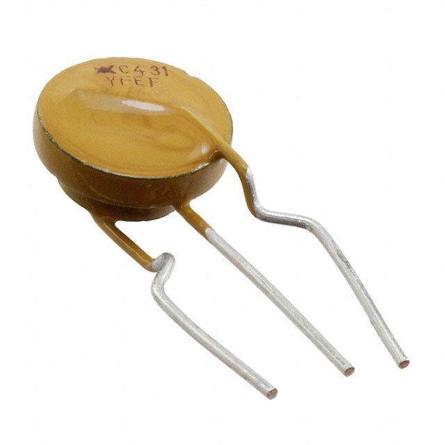
| 产品图片 |
|
| rohs | 符合RoHS无铅 / 符合限制有害物质指令(RoHS)规范要求 |
| 产品系列 | 接口 IC,接口 - 专用,STMicroelectronics CLT3-4BT6CLT |
| 数据手册 | |
| 产品型号 | CLT3-4BT6 |
| 产品种类 | Voltage Protection Devices |
| 产品类型 | Digital Termination |
| 供应商器件封装 | 20-TSSOP |
| 其它名称 | 497-12485-5 |
| 其它有关文件 | http://www.st.com/web/catalog/sense_power/FM114/SC480/PF66610?referrer=70071840 |
| 功率(W) | - |
| 包装 | 管件 |
| 单位重量 | 74 mg |
| 商标 | STMicroelectronics |
| 安装风格 | SMD/SMT |
| 封装 | Tube |
| 封装/外壳 | 20-TSSOP(0.173",4.40mm 宽) |
| 封装/箱体 | TSSOP-20 |
| 工作电源电压 | 10 V |
| 工厂包装数量 | 74 |
| 应用 | 通用 |
| 技术 | 混合技术 |
| 最大工作温度 | + 85 C |
| 最小工作温度 | - 25 C |
| 标准包装 | 74 |
| 电压-工作 | - |
| 电压-箝位 | - |
| 电源电流 | 0.0008 A |
| 电路数 | 4 |
| 系列 | CLT3-4B |


- 商务部:美国ITC正式对集成电路等产品启动337调查
- 曝三星4nm工艺存在良率问题 高通将骁龙8 Gen1或转产台积电
- 太阳诱电将投资9.5亿元在常州建新厂生产MLCC 预计2023年完工
- 英特尔发布欧洲新工厂建设计划 深化IDM 2.0 战略
- 台积电先进制程称霸业界 有大客户加持明年业绩稳了
- 达到5530亿美元!SIA预计今年全球半导体销售额将创下新高
- 英特尔拟将自动驾驶子公司Mobileye上市 估值或超500亿美元
- 三星加码芯片和SET,合并消费电子和移动部门,撤换高东真等 CEO
- 三星电子宣布重大人事变动 还合并消费电子和移动部门
- 海关总署:前11个月进口集成电路产品价值2.52万亿元 增长14.8%


PDF Datasheet 数据手册内容提取
CLT3-4B Current limited over-voltage protected quad digital termination Features ■ 4 channel topology ■ Wide range input dc Voltage: – V= - 0.3 to 30 V with R = 0 I I – V = - 30 to 30 V with R = 1.8 kΩ I I TSSOP20 – Low side configuration with common ground ■ Current limiter: Applications – I = 3 mA GEN – Input current limiter activation voltage < 5 V ■ Industrial automation – Temperature compensated operation ■ Programmable logic controller ■ Opto-coupler drive: – No coupler activation below 1.5 mA input ■ Communication field bus nodes current ■ Peripheral input / output modules ■ Input protection (R = 1.2 kΩ): I ■ Machine tool interface – IEC 61000-4-2 electrostatic discharge ESD, Class 3 In contact, ± 6 kV; in air, ± 8 kV Description Level B: temporary disruption; no The CLT3-4 is a quadruple input digital change of opto-coupler state termination device designed for 24 V dc – IEC 61000-4-5 voltage surge, Class 3 automation applications. It provides the front-end ± 1000 V with 42 Ω serial resistor in circuitry of a digital input module (I/O) in industrial differential mode automation, and drives an isolating opto-coupler. Level B: temporary disruption – IEC 61000-4-4 transient burst immunity Figure 1. Pin configuration ± 4 kV peak voltage; 5 kHz repetitive rate OUT1 OUT2 COM COM34 COM Level A: fully functional COM COM12 COM OUT3 OUT4 ■ Operating ambient temperature: - 25 to 85° C 20 19 18 17 16 15 14 13 12 11 Benefits ■ Reduced overall dissipation ■ Compact with high integration 1 2 3 4 5 6 7 8 9 10 ■ Enables input to meet type 1 and 3 characteristic of IEC 61131-2 standard IN IN2 ESDC ESD34 COM COM ESD12 VC IN3 IN4 ■ Compatible operation with 2 and 3 wires The pins ESD, COM , COM (pins # 1, 3, 6, 8, 10, 11, proximity sensor according EN60947-5-2 IJ 13, 15, 16, 18, 20) must be connected together standard externally. This common pad COM is enlarged to ■ Insensitive to the on state sensor impedance reduce the thermal resistance and improve the device ■ Surface mount package for highly automated cooling. The COM and IN pins are designed to assembly minimize the EMI effects on the circuit. ■ Enhanced functional reliability November 2007 Rev 5 1/13 www.st.com
Characteristics CLT3-4B 1 Characteristics Figure 2. Functional block diagram OPTO COUPLER DRIVER IN1 OUT1 OEVSEDR I1 0.25x0IL.7IM5xILIM I1 PRVOOTLETCAGTIEON CURRENT LIMITER ILIM 1.5mA ESD12 COM12 ESD VOOLVTEARGE CURRENT LIMITER ILIM 1.5mA PROTECTION 0.25xILIM I2 0.75xILIM I2 IN2 OUT2 OPTO COUPLER DRIVER Vc ESD BIASING Volt Prot CIRCUIT TO COMPARATORS ESDC COM OPTO COUPLER DRIVER IN3 OUT3 I3 0.75xILIM I3 ESD 0.25xILIM OVER VOLTAGE CURRENT LIMITER ILIM 1.5mA PROTECTION ESD34 COM34 ESD OVER CURRENT LIMITER ILIM 1.5mA VOLTAGE PROTECTION 0.25xILIM I4 0.75xILIM I4 IN4 OUT4 OPTO COUPLER DRIVER T able 1. Absolute ratings (limiting values) Symbol Parameter Value Unit Supply steady state voltage, R = 0 kΩ - 0.3 to 30 V C V V CC C Supply steady state voltage, R = 4.7 kΩ - 30 to 30 V C Input steady state voltage, R = 0 kΩ - 0.3 to 30 V I Input steady state voltage, R = 1.2 kΩ - 0.3 to 32 V I VI (1) IN Input repetitive pulse voltage, RI = 1.2 kΩ - 0.3 to 35 V Input repetitive pulse voltage, - 30 to 30 V R = 1.8 kΩ, R = 4.7 kΩ (2) I C Input maximum forward current, 5 mA R = 1.2 kΩ, R = 4.7 kΩ I C I IN IN Input maximum reverse current, 20 mA R = 1.8 kΩ, R = 4.7 kΩ (2) I C V OUT Maximum output steady state voltage 2.5 V OM I OUT Output current - 4 to 4 mA OM T Operating ambient temperature - 25 to 85 ° C AMB AII T Operating and storage junction temperature - 25 to 150 ° C J 1. V = V + R x I ; V = voltage at the input pin itself I IN I IN IN 2. According to test diagram and design recommendations described in Section2.2. 2/13
CLT3-4B Characteristics T able 2. Thermal resistance Symbol Parameter Value Unit TSSOP20 thermal resistance junction to ambient R 90 °C/W th(j-a) Board copper surface = 2 cm , copper thickness = 35 µm 2 T able 3. Electrical characteristics (T = 25 °C, V = 24 V and COM pin voltage J CC referred unless otherwise specified) Symbol Pin Name Conditions Min. Typ Max. Unit Current limitation V = 0.9 to 2.0 V OUT I IN Input limiting current V = 5 to 27 V 2.1 3 3.7 mA LIM IN T = - 25 to 85° C AMB Maximum off state V IN I = 100 µA 1.5 V LOW voltage IN V IN Activation threshold I = 2.1 mA 3.4 5 V TH IN Input and Supply Protection V IN Clamping voltage I = 7 mA; t = 1 ms 31 38 - V CL IN P Opto-coupler driver operation V = 5 V, (1) - 10 40 µA I I OUT Off state output current OFF I = 1.5 mA, (2) - 10 40 µA IN V OUT Off state output voltage I = 1.5 mA 0.15 0.5 V OFF IN V = 5 V 1.5 2 - mA IN I OUT On state output current ON V = 4.2 V, V = 10 V 1.5 2 - mA IN C Supply and biasing circuit V V Supply voltage T = - 25 to 85° C 10 V C C AMB I V Supply current V = V = 30 V 550 800 µA C C IN C 1. According to Figure9: Robust application diagram on page8 with use of a R = 1.8 kΩ resistor, and an opto-coupler (R (0 V) = 15 kΩ) I LED 2. According to Figure9: Robust application diagram on page8 with use of a R = 0 kΩ resistor, and an opto-coupler (R (0 V) = 15 kΩ) I LED T able 4. Switching electrical characteristics (T = 25 °C, V = 24V and COM pin J CC voltage referred unless otherwise specified) Symbol Pin Name Conditions Min. Typ Max. Unit F IN-OUT Input to output running frequency 5 kHz MAX t IN-OUT Input activation propagation time C = 22 nF 6 µs PLH OUT t IN-OUT Input de-activation propagation time C = 22 nF 10 µs PHL OUT 3/13
Characteristics CLT3-4B T able 5. CLT3 System electromagnetic compatibility ratings, R = 1.8 kΩ, R = 4.7 kΩ (unless otherwise specified) I C Symbol Node Parameter name and conditions Value Unit ESD protection, IEC 61000-4-2, per input, in air ± 8 kV ESD protection, IEC 61000-4-2, per input, in contact ± 6 kV V IN PP ESD protection, IEC 61000-4-2, per input, in air, R = 0 Ω ± 3 kV I ESD protection, IEC 61000-4-2, per input, in contact, R = 0 Ω ± 3 kV I Total Peak Pulse Voltage Burst, IEC 61000-4-4 V V ± 4 kV PPB I C = 100 pF, C = 22 nF, F = 5 kHz (1) IN OUT V V Peak Pulse Voltage Surge, IEC 61000-4-5, R = 42 Ω (2) ± 1 kV PP I V V Peak Pulse Voltage Surge, IEC 61000-4-5, R = 2 Ω (2) ± 1 kV PP CC 1. Refer to Application note AN2527 for test conditions. 2. See test circuit in Figure12. Figure 3. Typical junction to ambient thermal resistance versus copper surface under common pad (FR4 epoxy, copper thickness is 35 µm) Rth(j-a)(° C/W) 160 140 120 100 80 60 40 20 S(cm²) 0 0.0 0.5 1.0 1.5 2.0 2.5 3.0 3.5 4.0 4.5 5.0 1.1 Functional description The CLT3-4 is a quadruple input digital termination device designed for 24 V DC automation applications. It provides the front-end circuitry of a digital input module (I/O) in industrial automation, and drives an isolating opto-coupler. Available in a four channels configuration, it offers a high-density termination by minimizing the external components count. It is housed in a TSSOP20 surface mount package to reduce the printed board size. Made of an input voltage protection, a serial current limiting circuit and an opto-coupler driver, each channel circuit terminates the connection between the logic input and the associated high side sensor or switch. The CLT3-4 is a 3mA quad channel device compatible the type 1 and 3 characteristics of the IEC61131-2 standard. Each input voltage clamping block protects the module input against electromagnetic interferences such as those described in the IEC 61131-2 standard and IEC 61000-4-2 (ESD), 4-4 (transient burst), 4-5 (voltage surge) standards. The supply input is also designed with such a protection structure. 4/13
CLT3-4B Characteristics The current limiting circuit connected between the input and the output pins is compensated all over the temperature range. Thanks to its low tolerance, the current limitation allows reducing drastically the dissipation of the input compared to a resistive input: the overall module requires less cooling capability and becomes smaller. The output block of each termination channel controls the operation of an opto-coupler that is enabled by a Light Emitting Diode. When the input current is less than 1.5 mA, this output circuit derivates the input current to maintain the opto-coupler off. The original structure of the CLT limiter allows its activation threshold to be low and insensitive to the output voltage up to a maximum value of 2.0 V. When the CLT input voltage V is higher than 5 V, or the module input voltage Vi higher IN than 11 V and a series resistor R = 1.2 kΩ, the output current that is a share of the input I current (3/4) is higher than 1.5 mA. The whole termination channel including the opto- coupler is on. Depending on the input type operation that is described by the IEC 61131-2 standard, the input resistance R can be adjusted because of the different on-state threshold V . I ON MIN This document describes operation and characteristics for type 3 operation with V = 11 V and R = 1.2 kΩ. ON MIN I In type 1 operation the on state threshold V is 12.34 V instead, and the input resistor ON MIN R is set 2.2 kΩ. I 1.2 Input characteristics of CLT3-4 Figure 4. Typical input characteristics of each CLT3-4 channel VIN(V) 30 30 25 3.7 20 15 10 On-state 5 5 Off-state 0 0 0.5 1 1.5 2 2.5 3 3.5 4 IIN(mA) 5/13
Characteristics CLT3-4B Figure 5. T ypical current limiter variation Figure 6. Typical limiter threshold voltage versus junction temperature variation versus junction 0.9 V < V < 2 V temperature for I = 2.1 mA OUT IN IIim/ IIim(25° C) VTH(V) 102% 3.6 100% V = 27V 98% IN 3.5 96% 94% 3.4 92% V = 5V IN 90% 3.3 88% 86% Tj(°C) Tj(° C) 84% 3.2 -25 0 25 50 75 100 125 -25 0 25 50 75 100 125 1.3 CLT3-4 Input / output transfer characteristics (with respect to common pin COM) Figure 7. Current tranfer characteristic Figure 8. Transconductance characteristic IO4UT(mA) IOUT(mA) 4 23..535 Forbidden Transition zone 2.1 ISOLATOR ON 3.7 23..553 ISOLATOR ON 2 2 1.5 1.5 1 1 0.04 Transition zone 0.5 0.5 0 0 0 0.5 1 1.5 2 2.5 3 3.5 4 0 5 10 15 20 25 30 ISOLATOR OFF IIN(mA) VI(V) 6/13
CLT3-4B Application information 2 Application information 2.1 Application description The CLT device is used between the input module and the opto-coupler of an I/O module. To secure the coupler off state and the non-conduction of its diode, the maximum CLT output current is 40 µA with Ropto = 15 kΩ. When the CLT input voltage V is higher than 5 V, a IN minimum CLT output current of 1.5mA will secure the opto-coupler on state. The CLT limiter is insensitive to the output voltage up to 2.0V. Therefore, its output is able to drive any state of the art opto-coupler. Some additional device can be added in series with the opto-coupler if the output voltage remains within its functional limits. A stand-alone sensor is normally connected on the CLT input. For a good off state control, its quiescent current has to be less than 1.5 mA (EN60947-5-2 standard compatible) keeping then the opto-coupler off thanks to the CLT device (I < 40 µA). And its maximum OUT ON state voltage V will be lower than 8 V (EN60947-5-2 standard compatible) S-ON corresponding to the difference between the minimum supply voltage (V = 19.2 V) CC MIN and the maximum current limitation activation voltage: V = V + V CC MIN S-ON I V = V + R x I I IN I IN MAX (V = 11 V when V = 5 V, R = 1.2 kΩ, I < 3.7 mA). I IN I IN 2.2 Input reverse polarity robustness Each input of the CLT device may be biased to a reverse polarity. This case corresponds to a connection mistake or a reverse biasing that is generated by the demagnetization of a monitored inductive solenoid. The involved input can withstand the reverse current up to 20 mA (in the configuration shown in Figure10) through its input protection diode while its opto-coupler remains OFF. Such a case is not critical for the CLT3-4 itself, as it represents less than 15 mW per disturbed input. But the input resistors should be designed with care regardless of their thermal characteristics (refer to Application note AN2527). When the reverse polarity operation is required in types 3 input mode, it is recommended to increase the input resistance R to 1.8 kΩ in order to reduce its dissipation and keep the I input current below its maximum allowed level (20 mA). The surge and transient immunity robustness of the CLT3 is then also increased. A 1.8 kΩ value allows the reverse input current to be reduced to 16.2 mA and the resistor dissipation to be reduced to 0.47 W, for 30 V V and a - 30 V V voltages. CC I The CLT3 normal operation in type 3 is fully compatible with this recommended resistance since its internal state threshold is monitored at V = 4.2 V and V = 10V - corresponding to IN C V = 11 V and V = 19 V. I CC In type 1 input operation where R = 2.2 kΩ the dissipation of this resistor is less than I 0.39W. The other inputs remain operational, as long as the power supply is working properly (V >19 V). Refer to Application note AN 2527 for representative application design case. CC 7/13
Application information CLT3-4B The CLT3-4 and the 24 V bus power supply have the same ground COM = GND. The reverse polarity of the power supply will shutdown the device. And the power supply resistor R will limit the default current protecting the power supply pin V . Its dissipation will be less C C than 0.2 W. Then, the whole module supply voltage rating is extended to from 0 to 30 V to -30 to +30 V. 2.3 EMC considerations Figure9 gives a typical application diagram where output capacitors are used to increase CLT device immunity against fast transient bursts. Figure11 gives the printed circuit board layout associated with this schematic. Refer to AN2527 for EMC considerations. Figure 9. Robust application diagram 1 COM COM VV V II IN 2 wires sensor IN111 OUT111 R I 24V ESD111222 COM111222 R SUPPLY 3 wires sensor I IN222 OUT222 VCC VC VCCC COM R C ESDCCC COM R I Contact switch IN3 OUT333 ESD COM 34 34 R I 2 wires sensor IN OUT 4 4 COM COM 8/13
CLT3-4B Application information Figure 10. Current sharing in the CLT device when IN is biased at - 30 V and the 4 others at + 30 V, R = 1.8 kΩ I 4.7 kΩ 0.8 mA VV Vcc = + 30V CC 3.7 mA IINNNN VCL= 38V IIRREEGG NN OOUUTT11 II = + 30V 11 1.8 kΩ OOPPTTOO NN GND (0V) CCOOMM OOPPTTOO 44 1.8 kΩ II ==--30V 22 16.2 mA IINN44 IIRREEGG44 OOUUTT22 CCLLTT33--44 Figure 11. TSSOP20 printed circuit board example CCOOMMMMOONN PPAADD MMOODDUULLEE CCOONNNNEECCTTOORR CCCOOOMMM CCCOOOMMM IIINNN111 OOOUUUTTT111 EEESSSDDD111222 CCCOOOMMM111222 IIINNN222 OOOUUUTTT222 VVVCCC CCCOOOMMM EEESSSDDDCCC CCCOOOMMM IIINNN OOOUUUTTT 333 333 EEESSSDDD CCCOOOMMM 333444 333444 IIINNN OOOUUUTTT 444 444 CCCOOOMMM CCCOOOMMM GGNNDD CCOOOOLLIINNGG PPAADD The input and supply pins are designed to withstand electromagnetic interferences. As shown on the device block diagram, each channel input is protected by a clamping diode that is connected to the common pin COM. Combined with a serial input resistance R = 1.2kΩ, this clamping diode implements an effective protection against transient voltage I burst (± 4 kV, IEC 61000-4-4) and voltage surge (± 1 kV, IEC 61000-4-5). 9/13
Application information CLT3-4B Depending on the input type operation the input resistance R can be adjusted because of I the different on-state threshold V . So the surge voltage is also increased from the ON MIN minimum level of the type 3 to the type as shown in Table6. T able 6. Setting the input resistor R according to the input type operation I Type V (V) R (kΩ) V surge (kV) ON MIN I PP 1 15 2.2 2 3 11 1.2 to 1.8 1 This combination allows the surge voltage to be applied from each input to other inputs, the ground and the supply contacts in differential or common modes (see Figure12). Thanks to its high resistance R = 4.7 kΩ, the supply pin V withstands IEC 61000-4-5 with C C ±1000V surge voltage (see Figure12). Finally, an external output capacitor may be placed in parallel with the opto-coupler diode to filter the transient disturbances injected in the inputs of the module and secure the immunity of the opto-coupler itself. Figure 12. Input pin IN and supply pin V voltage surge test circuit C VVPPPPSS= ±1 kV with 2Ω VVCCCC RRCC VV CC RR II VVPPPPII IINN11 VVV II PPPPPP RR II IINN VV 22 PPPPSS VV = ±1 kV with 42Ω PPPPII RR II CLT3-4 VV PPPPII GGNNDD CCOOMM PP 55nnFF PPEE//FFEE 10/13
CLT3-4B Package information 3 Package information ● Epoxy meets UL94,V0 In order to meet environmental requirements, ST offers these devices in ECOPACK® packages. These packages have a lead-free second level interconnect. The category of second level interconnect is marked on the package and on the inner box label, in compliance with JEDEC Standard JESD97. The maximum ratings related to soldering conditions are also marked on the inner box label. ECOPACK is an ST trademark. ECOPACK specifications are available at: www.st.com. T able 7. TSSOP20 dimensions Dimensions Ref. Millimeters Inches Min. Typ. Max. Min. Typ. Max. D E1 A 1.2 0.047 A2 A A1 0.05 0.15 0.002 0.006 b A1 C A2 0.8 1.0 1.05 0.031 0.039 0.041 aaa C b 0.19 0.3 0.007 0.012 PIN 1 INDENTIFICATION 20 11 E SpelCaatnineg G0a.g2e5 pmlamne DEc 066...0429 66..54 660...662 000...220540243 00..225562 000...022055796 E1 4.3 4.4 4.5 0.169 0.173 0.177 L k e 0.65 0.026 1 10 L1 L 0.45 0.6 0.75 0.017 0.023 0.029 e L1 1.0 0.039 k 0° 8° 0° 8° aaa 0.1 0.004 Figure 13. TSSOP20 footprint (dimensions in mm) 7.26 4.93 0.36 6.21 0.65 11/13
Ordering information CLT3-4B 4 Ordering information T able 8. Ordering information Order code Marking Package Weight Base qty Delivery mode CLT3-4BT6 CLT3-4B TSSOP20 0.074 g 74 Tube CLT3-4BT6-TR CLT3-4B TSSOP20 0.074 g 2500 Tape and reel 5 Revision history T able 9. Document revision history Date Revision Changes August-2002 4A Previous release. Reformatted and restructured to current standard. Updated Figure2, Figure9, Figure10, Figure11, and deleted Figure 12. 27-Nov-2007 5 Added paragraphs to Functional description and Application information. Extended application field with a new diagram (Figure11) for reverse polarity test. Updated Package information. 12/13
CLT3-4B Please Read Carefully: Information in this document is provided solely in connection with ST products. STMicroelectronics NV and its subsidiaries (“ST”) reserve the right to make changes, corrections, modifications or improvements, to this document, and the products and services described herein at any time, without notice. All ST products are sold pursuant to ST’s terms and conditions of sale. Purchasers are solely responsible for the choice, selection and use of the ST products and services described herein, and ST assumes no liability whatsoever relating to the choice, selection or use of the ST products and services described herein. No license, express or implied, by estoppel or otherwise, to any intellectual property rights is granted under this document. If any part of this document refers to any third party products or services it shall not be deemed a license grant by ST for the use of such third party products or services, or any intellectual property contained therein or considered as a warranty covering the use in any manner whatsoever of such third party products or services or any intellectual property contained therein. UNLESS OTHERWISE SET FORTH IN ST’S TERMS AND CONDITIONS OF SALE ST DISCLAIMS ANY EXPRESS OR IMPLIED WARRANTY WITH RESPECT TO THE USE AND/OR SALE OF ST PRODUCTS INCLUDING WITHOUT LIMITATION IMPLIED WARRANTIES OF MERCHANTABILITY, FITNESS FOR A PARTICULAR PURPOSE (AND THEIR EQUIVALENTS UNDER THE LAWS OF ANY JURISDICTION), OR INFRINGEMENT OF ANY PATENT, COPYRIGHT OR OTHER INTELLECTUAL PROPERTY RIGHT. UNLESS EXPRESSLY APPROVED IN WRITING BY AN AUTHORIZED ST REPRESENTATIVE, ST PRODUCTS ARE NOT RECOMMENDED, AUTHORIZED OR WARRANTED FOR USE IN MILITARY, AIR CRAFT, SPACE, LIFE SAVING, OR LIFE SUSTAINING APPLICATIONS, NOR IN PRODUCTS OR SYSTEMS WHERE FAILURE OR MALFUNCTION MAY RESULT IN PERSONAL INJURY, DEATH, OR SEVERE PROPERTY OR ENVIRONMENTAL DAMAGE. ST PRODUCTS WHICH ARE NOT SPECIFIED AS "AUTOMOTIVE GRADE" MAY ONLY BE USED IN AUTOMOTIVE APPLICATIONS AT USER’S OWN RISK. Resale of ST products with provisions different from the statements and/or technical features set forth in this document shall immediately void any warranty granted by ST for the ST product or service described herein and shall not create or extend in any manner whatsoever, any liability of ST. ST and the ST logo are trademarks or registered trademarks of ST in various countries. Information in this document supersedes and replaces all information previously supplied. The ST logo is a registered trademark of STMicroelectronics. All other names are the property of their respective owners. © 2007 STMicroelectronics - All rights reserved STMicroelectronics group of companies Australia - Belgium - Brazil - Canada - China - Czech Republic - Finland - France - Germany - Hong Kong - India - Israel - Italy - Japan - Malaysia - Malta - Morocco - Singapore - Spain - Sweden - Switzerland - United Kingdom - United States of America www.st.com 13/13
Mouser Electronics Authorized Distributor Click to View Pricing, Inventory, Delivery & Lifecycle Information: S TMicroelectronics: CLT3-4BT6 CLT3-4BT6-TR