ICGOO在线商城 > 电路保护 > TVS - 混合技术 > SP720ABG
 Datasheet下载
- 型号: SP720ABG
- 制造商: Littelfuse
- 库位|库存: xxxx|xxxx
- 要求:
| 数量阶梯 | 香港交货 | 国内含税 |
| +xxxx | $xxxx | ¥xxxx |
查看当月历史价格
查看今年历史价格
SP720ABG产品简介:
ICGOO电子元器件商城为您提供SP720ABG由Littelfuse设计生产,在icgoo商城现货销售,并且可以通过原厂、代理商等渠道进行代购。 SP720ABG价格参考¥12.65-¥16.25。LittelfuseSP720ABG封装/规格:TVS - 混合技术, 。您可以下载SP720ABG参考资料、Datasheet数据手册功能说明书,资料中有SP720ABG 详细功能的应用电路图电压和使用方法及教程。
Littelfuse Inc. 的 SP720ABG 是一款 TVS(瞬态电压抑制器)混合技术器件,主要用于保护电子设备免受瞬态电压尖峰的影响。这种器件广泛应用于各种需要高可靠性和稳定性的电路中,尤其是在面对静电放电(ESD)、电快速瞬变脉冲群(EFT)和雷击浪涌等威胁时。

 应用场景:

1. 通信设备:
   - 在基站、路由器、交换机和其他通信基础设施中,SP720ABG 可以保护信号线和电源线免受瞬态电压的损害。它能够有效地吸收由雷击或电力波动引起的瞬态能量,确保通信链路的稳定性。

2. 消费类电子产品:
   - 包括智能手机、平板电脑、笔记本电脑等便携式设备。这些设备通常暴露在复杂的电磁环境中,容易受到静电放电和瞬态电压的冲击。SP720ABG 能够提供可靠的保护,延长设备的使用寿命并提高用户的安全性。

3. 工业自动化系统:
   - 在工厂自动化、过程控制和机器人系统中,SP720ABG 可以用于保护传感器、执行器和其他关键组件。这些系统通常运行在恶劣的电气环境中,瞬态电压可能会导致严重的故障甚至停机,使用 SP720ABG 可以显著提高系统的可靠性和安全性。

4. 汽车电子:
   - 现代汽车中的电子控制系统(如发动机控制单元、车身控制模块、娱乐系统等)对瞬态电压非常敏感。SP720ABG 可以安装在这些系统的输入输出端口,防止外部干扰导致的损坏,确保车辆的正常运行。

5. 医疗设备:
   - 医疗设备如监护仪、超声波设备、心电图机等需要极高的稳定性和可靠性。SP720ABG 可以保护这些设备的关键电路,确保其在各种环境下都能正常工作,保障患者的安全。

6. 电力系统:
   - 在电力分配和传输系统中,SP720ABG 可以用于保护继电器、断路器和其他电力设备,防止因雷击或其他瞬态事件引起的损坏,确保电网的稳定运行。

总之,SP720ABG 以其卓越的瞬态电压抑制性能,广泛应用于多个领域,为各种电子设备提供了可靠的保护,确保其在复杂和恶劣的电气环境中依然能够稳定运行。
| 参数 | 数值 |
| 产品目录 | |
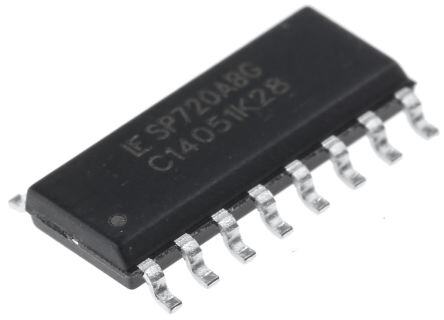
| 描述 | TVS ARRAY ESD 14CH 30V 16-SOICESD 抑制器 35V(SUP) 2A(I(IN)) 130THRM RES |
| 产品分类 | TVS - 其它复合ESD 抑制器 |
| 品牌 | Littelfuse |
| 产品手册 | |
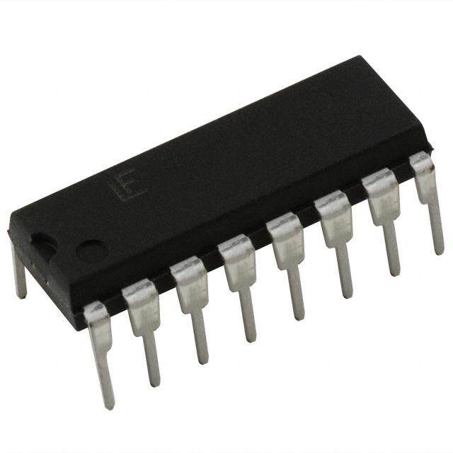
| 产品图片 |
|
| rohs | 符合RoHS无铅 / 符合限制有害物质指令(RoHS)规范要求 |
| 产品系列 | Littelfuse SP720ABG- |
| 数据手册 | |
| 产品型号 | SP720ABG |
| 产品培训模块 | http://www.digikey.cn/PTM/IndividualPTM.page?site=cn&lang=zhs&ptm=25590 |
| 产品目录绘图 |
|
| 产品目录页面 | |
| 产品种类 | ESD 抑制器 |
| 供应商器件封装 | 16-SOIC |
| 其它名称 | F2717 |
| 击穿电压 | 30 V |
| 功率(W) | - |
| 包装 | 管件 |
| 商标 | Littelfuse |
| 安装风格 | SMD/SMT |
| 封装 | Tube |
| 封装/外壳 | 16-SOIC(0.154",3.90mm 宽) |
| 封装/箱体 | SOIC-16 |
| 尺寸 | 4 mm W x 10 mm L x 1.75 mm H |
| 峰值浪涌电流 | 3 A |
| 工作温度范围 | - 40 C to + 105 C |
| 工作电压 | 2 V to 30 V |
| 工厂包装数量 | 960 |
| 应用 | 通用 |
| 技术 | 混合技术 |
| 最大工作温度 | + 105 C |
| 最小工作温度 | - 40 C |
| 极性 | Bidirectional |
| 标准包装 | 48 |
| 电压-工作 | 30V |
| 电压-箝位 | - |
| 电容 | 3 pF |
| 电路数 | 14 |
| 端接类型 | SMD/SMT |
| 系列 | SP720 SPA |
| 通道 | 14 Channels |
| 零件号别名 | 576-SP720AB SP720AB |


- 商务部:美国ITC正式对集成电路等产品启动337调查
- 曝三星4nm工艺存在良率问题 高通将骁龙8 Gen1或转产台积电
- 太阳诱电将投资9.5亿元在常州建新厂生产MLCC 预计2023年完工
- 英特尔发布欧洲新工厂建设计划 深化IDM 2.0 战略
- 台积电先进制程称霸业界 有大客户加持明年业绩稳了
- 达到5530亿美元!SIA预计今年全球半导体销售额将创下新高
- 英特尔拟将自动驾驶子公司Mobileye上市 估值或超500亿美元
- 三星加码芯片和SET,合并消费电子和移动部门,撤换高东真等 CEO
- 三星电子宣布重大人事变动 还合并消费电子和移动部门
- 海关总署:前11个月进口集成电路产品价值2.52万亿元 增长14.8%


PDF Datasheet 数据手册内容提取
TVS Diode Arrays (SPA® Diodes) General Purpose ESD Protection - SP720 Series SP720 Series 3pF 4kV Diode Array RoHS Pb GREEN Description The SP720 is an array of SCR/Diode bipolar structures for ESD and over-voltage protection to sensitive input circuits. The SP720 has 2 protection SCR/Diode device structures per input. A total of 14 available inputs can be used to protect up to 14 external signal or bus lines. Over-voltage protection is from the IN (pins 1-7 and 9-15) to V+ or V-. The SCR structures are designed for fast triggering at a threshold of one +V diode threshold above V+ (Pin 16) or BE a -V diode threshold below V- (Pin 8). From an IN input, BE a clamp to V+ is activated if a transient pulse causes the input to be increased to a voltage level greater than one V above V+. A similar clamp to V- is activated if a negative Pinout BE pulse, one V less than V-, is applied to an IN input. BE Standard ESD Human Body Model (HBM) Capability is: IN 1 16 V+ IN 2 15 IN Features IN 3 14 IN IN 4 13 IN • ESD Interface Capability for HBM Standards SP720 (PDIP, SOIC) IN 5 12 IN - MIL STD 3015.7 .................................................15kV TOP VIEW IN 6 11 IN - IEC 61000-4-2, Direct Discharge, IN 7 10 IN - Single Input ..........................................4kV (Level 2) V- 8 9 IN - Two Inputs in Parallel ............................8kV (Level 4) - IEC 61000-4-2, Air Discharge ...............15kV (Level 4) • High Peak Current Capability Functional Block Diagram - IEC 61000-4-5 (8/20µs) .......................................±3A V+ 16 - Single Pulse, 100µs Pulse Width ........................±2A - Single Pulse, 4µs Pulse Width ............................±5A • Designed to Provide Over-Voltage Protection - Single-Ended Voltage Range to ........................+30V 3 - 7 - Differential Voltage Range to ............................±15V IN 9 - 15 IN 1 2 IN • Fast Switching ..............................................2ns Risetime • Low Input Leakages .................................1nA at 25º (Typ) • Low Input Capacitance .......................................3pF (Typ) • An Array of 14 SCR/Diode Pairs • Operating Temperature Range....................-40ºC to 105ºC V- 8 Applications • Microprocessor/Logic • Analog Device Input Additional Information Input Protection Protection • Data Bus Protection • Voltage Clamp Datasheet Resources Samples Life Support Note: Not Intended for Use in Life Support or Life Saving Applications The products shown herein are not designed for use in life sustaining or life saving applications unless otherwise expressly indicated. © 2017 Littelfuse, Inc. Specifications are subject to change without notice. Revised: 02/23/17
TVS Diode Arrays (SPA® Diodes) General Purpose ESD Protection - SP720 Series Absolute Maximum Ratings Thermal Information Parameter Rating Units Parameter Rating Units Thermal Resistance (Typical, Note 1) θ oC/W Continuous Supply Voltage, (V+) - (V-) +35 V JA PDIP Package 90 oC/W Forward Peak Current, I to V , I to GND IN CC IN ±2, 100µs A (Refer to Figure 5) SOIC Package 130 oC/W CAUTION: Stresses above those listed in “Absolute Maximum Ratings” may cause Maximum Storage Temperature Range -65 to 150 oC permanent damage to the device. This is a stress only rating and operation of the device Maximum Junction Temperature (Plastic at these or any other conditions above those indicated in the operational sections of this Package) 150 oC specification is not implied. Note: Maximum Lead Temperature 260 oC ESD Ratings and Capability - See Figure 1, Table 1 (Soldering 20-40s) (SOIC Lead Tips Only) Load Dump and Reverse Battery (Note 2) 1. θ is measured with the component mounted on an evaluation PC board in free air. JA Electrical Characteristics T = -40oC to 105oC, V = 0.5V , Unless Otherwise Specified A IN CC Parameter Symbol Test Conditions Min Typ Max Units Operating Voltage Range, V - 2 to 30 - V SUPPLY V = [(V+) - (V-)] SUPPLY Forward Voltage Drop: I = 1A (Peak Pulse) IN IN to V- V - 2 - V FWDL IN to V+ V - 2 - V FWDH Input Leakage Current I -20 5 20 nA IN Quiescent Supply Current I - 50 200 nA QUIESCENT Equivalent SCR ON Threshold Note 3 - 1.1 - V Equivalent SCR ON Resistance V /I ; Note 3 - 1 - Ω FWD FWD Input Capacitance C - 3 - pF IN Input Switching Speed t - 2 - ns ON Notes: 2. In automotive and battery operated systems, the power supply lines should be externally protected for load dump and everse battery V+ and V- pins are connected to the same supply voltage source as the device or control line under protection, a current limiting resistor should be connected in series between the external supply and the SP720 supply pins to limit reverse battery current to within the rated maximum limits. Bypass capacitors of typically 0.01µF or larger from the V+ and V- pins to ground are recommended. 3. Refer to the Figure 3 graph for definitions of equivalent “SCR ON Threshold” and “SCR ON Resistance.” These characteristics are given here for thumb-rule nformation to determine peak current and dissipation under EOS conditions. Typical Application of the SP720 (Application as an Input Clamp for Over-voltage, greater than 1V BE Above V+ or less than -1V below V-) BE +VCC +VCC INPUT DRIVERS LINEAR OR OR DIGITAL IC SIGNAL INTERFACE SOURCES IN 1-7 IN 9-15 TO +VCC V+ SP720 V- SP720 INPUT PROTECTION CIRCUIT (1 OF 14 ON CHIP) FIGURE 4.TYPICAL APPLICATION OF THE SP720 AS AN INPUT CLAMP FOR OVER-VOLTAGE, GREATER THAN 1VBE ABOVE V+ OR LESS THAN -1VBE BELOW V- © 2017 Littelfuse, Inc. Specifications are subject to change without notice. Revised: 02/23/17
TVS Diode Arrays (SPA® Diodes) General Purpose ESD Protection - SP720 Series ESD Capability ESD capability is dependent on the application and defined Figure 1: Electrostatic Discharge Test test standard. The evaluation results for various test standards and methods based on Figure 1 are shown in Table 1. R1 RD For the “Modified” MIL-STD-3015.7 condition that is CHARGE DISCHARGE SWITCH SWITCH defined as an “in-circuit” method of ESD testing, the V+ and V- pins have a return path to ground and the SP720 H.V. CD IN ESD capability is typically greater than 15kV from 100pF SUPPLY DUT through 1.5kΩ. By strict definition of MIL-STD-3015.7 using VD “pin-to-pin” device testing, the ESD voltage capability IEC 1000-4-2: R150 to 100M is greater than 6kV. The MIL-STD-3015.7 results were MIL STD 3015.7: R11 to 10M determined from AT&T ESD Test Lab measurements. FIGURE 1. ELECTROSTATIC DISCHARGE TEST The HBM capability to the IEC 61000-4-2 standard is Table 1: ESD Test Conditions greater than 15kV for air discharge (Level 4) and greater than 4kV for direct discharge (Level 2). Dual pin capability (2 Standard Type/Mode R C ±V adjacent pins in parallel) is well in excess of 8kV (Level 4). D D D Modified HBM 1.5kΩ 100pF 15kV For ESD testing of the SP720 to EIAJ IC121 Machine MIL STD 3015.7 Standard HBM 1.5kΩ 100pF 6kV Model (MM) standard, the results are typically better than HBM, Air Discharge 330Ω 150pF 15kV 1kV from 200pF with no series resistance. HBM, Direct Discharge 330Ω 150pF 4kV IEC 61000-4-2 HBM, Direct Discharge, 330Ω 150pF 8kV Two Parallel Input Pins EIAJ IC121 Machine Model 0kΩ 200pF 1kV Figure 2: Low Current SCR Forward Voltage Drop Curve Figure 3: High Current SCR Forward Voltage Drop Curve 100 2.5 TA = 25°C TA = 25°C SINGLE PULSE SINGLE PULSE FORWARD SCR CURRENT (mA) 86420000 FORWARD SCR CURRENT (A) 01..2515 ETQHRUEIVS. HSOATL.D O ~N 1.1V VFWD IFWD 0 0 600 800 1000 1200 0 1 2 3 FORWARD SCR VOLTAGE DROP (mV) FORWARD SCR VOLTAGE DROP (V) © 2017 Littelfuse, Inc. Specifications are subject to change without notice. Revised: 02/23/17
TVS Diode Arrays (SPA® Diodes) General Purpose ESD Protection - SP720 Series Peak Transient Current Capability for Long Duration Surges The peak transient current capability rises sharply as the Figure 4: Typical SP720 Peak Current Test Circuit width of the current pulse narrows. Destructive testing with a Variable Pulse Width Input was done to fully evaluate the SP720’s ability to withstand a wide range of transient current pulses. The circuit used to generate current pulses is shown in Figure 4. VARIABLE TIME DURATION + R1 CURRENT PULSE GENERATOR The test circuit of Figure 4 is shown with a positive pulse -VG CUSERNRESNET input. For a negative pulse input, the (-) current pulse input (-) goes to an SP720 ‘IN’ input pin and the (+) current pulse (+) input goes to the SP720 V- pin. The V+ to V- supply of the 1 IN V+16 SP720 must be allowed to float. (i.e., It is not tied to the 2 IN IN 15 ground reference of the current pulse generator.) Figure 3 IN IN 14 + 5 shows the point of overstress as defined by increased 4 IN SP720 IN 13 C1 - VOLTAGE 5 IN IN 12 leakage in excess of the data sheet published limits. PROBE 6 IN IN 11 The maximum peak input current capability is dependent 7 IN IN 10 on the V+ to V- voltage supply level, improving as the RVG1 ~AD 1J0. 1 0TVY/PAICT AYLPICAL 8 V- IN 9 supply voltage is reduced. Values of 0, 5, 15 and 30 C1 ~ 100 µF voltages are shown. The safe operating range of the FIGURE 5. TYPICAL SP720 PEAK CURRENT TEST CIRCUIT transient peak current should be limited to no more than Figure 5: SP720W TITyHp Ai cVAaRl INABoLEn PreULpSeEt WitIiDvTeH PINePaUkT Current 75% of the measured overstress level for any given pulse Pulse Capability width as shown in Figure 5. Showing the Measured Point of Overstress in Amperes vs When adjacent input pins are paralleled, the sustained pulse width time in milliseconds (T = 25oC) peak current capability is increased to nearly twice that A of a single pin. For comparison, tests were run using dual 10 pin combinations 1+2, 3+4, 5+6, 7+9, 10+11, 12+13 and CAUTION: SAFE OPERATING CONDITIONS LIMIT 9 THE MAXIMUM PEAK CURRENT FOR A GIVEN 14+15. PULSE WIDTH TO BE NO GREATER THAN 75% 8 OF THE VALUES SHOWN ON EACH CURVE. SINGLE PIN STRESS CURVES The overstress curve is shown in Figure 5 for a 15V supply A)7 DUAL PIN STRESS CURVE condition. The dual pins are capable of 10A peak current NT (6 E for a 10µs pulse and 4A peak current for a 1ms pulse. The RR5 complete for single pulse peak current vs. pulse width time K CU4 ranging up to 1 second are shown in Figure 5. A PE3 0V 15V 5V 2 30V 15V 1 V+ T OV-SUPPLY 0 0.001 0.01 0.1 1 10 100 1000 PULSE WIDTH TIME (ms) © 2017 Littelfuse, Inc. Specifications are subject to change without notice. Revised: 02/23/17
TVS Diode Arrays (SPA® Diodes) General Purpose ESD Protection - SP720 Series Soldering Parameters Reflow Condition Pb – Free assembly tP TP CCrriittiiccaall ZZoonnee - Temperature Min (Ts(min)) 150°C e RRaammpp--uupp TTLL ttoo TTPP Pre Heat -- TTeimmep e(mraitnu rteo Mmaaxx )( T(ts()max)) 2600 0–° C180 secs rutare TS(mTaxL) tL s pm RRaammpp--ddoown Average ramp up rate (Liquidus) Temp e PPrreehheeaatt 5°C/second max T (TL) to peak TS(min) tS T to T - Ramp-up Rate 5°C/second max S(max) L Reflow -- TTeemmppeerraattuurree ((TtL)) (Liquidus) 26107 –° C1 50 seconds 25 time to peak temperature Time L Peak Temperature (T ) 260+0/-5 °C P Time within 5°C of actual peak 20 – 40 seconds Temperature (t ) p Ramp-down Rate 5°C/second max Time 25°C to peak Temperature (T ) 8 minutes Max. P Do not exceed 260°C Package Dimensions Dual-In-Line Plastic Packages (PDIP) Package PDIP N E1 Pins 16 Lead Dual-in-Line INDEX AREA 1 2 3 N/2 JEDEC MS-001 -B- Millimeters Inches -A- Notes D E Min Max Min Max BASE A - 5.33 - 0.210 4 PLANE -C- A2 A SEATING A1 0.39 - 0.015 - 4 PLANE L CL A2 2.93 4.95 0.115 0.195 - D1 D1 A1 eA B1 B e eC C B 0.356 0.558 0.014 0.022 - 0.010 (0.25) M C A B S eB B1 1.15 1.77 0.045 0.070 8, 10 C 0.204 0.355 0.008 0.014 - NOTES: Notes: 1. ControllingD imensions:I NCH. In case of conflictb etweenE nglisha nd D 18.66 19.68 0.735 0.775 5 1. Controlling Dimensions: INCH. in case of conflict between English and Metric dimensMioentsr,i cthd eim inechn sdiiomnesn,ts hioen isn ccohn dtrioml.ensionsc ontrol. D1 0.13 - 0.005 - 5 2. Dim2e.nDsiiomnienng sainodn tionlgear anndc tinogle prearn AcNinSgI pY e14r .A5MNS-1I9 Y821.4.5M-1982. 3. Sym3.boSlsy mareb doelsfia nreed d ine fithnee “dMi nO t hSee r“ieMs OSyS merbioels L Sisyt”m inb oSleL citsiot”ni n2 .S2 eocft Piounbl 2ic.a2t ioofn No. E 7.62 8.25 0.300 0.325 6 95. PublicationN o. 95. E1 6.10 7.11 0.240 0.280 5 4. Dim4e.nDsiiomnse nAs, iAo1n asAn d, AL 1a raen mde La asurere md weaitshu trheed pw acitkhat ghee s peaactekda gine J sEe-DatEeCd s inea JtEin-g plane gDaEuCge sGeSa-t3i.ng plane gauge GS-3. e 2.54 BSC 0.100 BSC - 5. D, D5.1,D a,n Dd 1E,1 a dnimd eEn1s idonims deon snioot ninsdc loud neo mt ionlcdl ufladsehm oor lpdrofl tarusshio onrs p. rMootrldu sfliaosnh so.r protrusMioonsld s flhaasll hn ootr epxrcoeterdu s0i.o01n0s s inhcahl l( n0.o2t5 emxmce).ed 0.010 inch (0.25mm). eA 7.62 BSC 0.300 BSC 6 6. E a6n.d E e Aa nadre meeAasaurreed m weitahs tuhree ldew adisth ct ohnes lteraaindesd c oton bsetr paeinrpeednt doi cbuela pr etorp deantudmic --C- . eB - 10.92 - 0.430 7 7. e andu ela ra rteo mdaetausmure d-C a-t t.he lead tips with the leads unconstrained. e must be zero oBr g7.reaetBeCr a.nd eC are measureda t the lead tips witht he leads unconCstrained. L 2.93 3.81 0.115 0.150 4 8. B1 maexiCm mumu sdtim bee nzseiroon so dr og rneoat tinecr.lude dambar protrusions. Dambar protrusions shall N 16 16 9 not exceed 0.010 inch (0.25mm). 8. B1 maximumd imensionsd o not included ambarp rotrusions.D ambar 9. N is thpe rmotarxuimsiuomn sns uhmalbl enro otf e txecrmeeinda l0 p.0o1s0it ioinnsc.h (0.25mm). 10. Cor9n.erN le iasd tsh e(1 m, Na,x Nim/2u amndn uNm/2 b+e 1ro ) ffo tre Erm8.3in, aEl1p 6o.3s,i tEio18n.s3., E28.3, E42.6 will have a B1 dimension of 0.030 - 0.045 inch (0.76 - 1.14mm). 10. Corner leads (1, N, N/2 and N/2 + 1) for E8.3, E16.3, E18.3, E28.3, E42.6 willh ave a B1 dimensiono f 0.030 - 0.045 inch (0.76 - 1.14mm). © 2017 Littelfuse, Inc. Specifications are subject to change without notice. Revised: 02/23/17
TVS Diode Arrays (SPA® Diodes) General Purpose ESD Protection - SP720 Series Package Dimensions — Small Outline Plastic Packages (SOIC) N Package SOIC IANRDEEAX H 0.25(0.010) M B M Pins 16 E JEDEC MS-012 -B- Millimeters Inches 1 2 3 Notes L Min Max Min Max SEATING PLANE A 1.35 1.75 0.0532 0.0688 - -A- D A h x 45o A1 0.10 0.25 0.0040 0.0098 - B 0.33 0.51 0.013 0.020 9 -C- C 0.19 0.25 0.0075 0.0098 - µ D 9.80 10.00 0.3859 0.3937 3 e A1 C E 3.80 4.00 0.1497 0.1574 4 B 0.10(0.004) e 1.27 BSC 0.050 BSC - 0.25(0.010) M C AM B S H 5.80 6.20 0.2284 0.2440 - Notes: h 0.25 0.50 0.0099 0.0196 5 1. Symbols are defined in the “MO Series Symbol List” in Section 2.2 of Publication L 0.40 1.27 0.016 0.050 6 Number 95. 2. DiNmOeTnsEioSn:ing and tolerancing per ANSI Y14.5M-1982. N 16 16 7 3. Dim1e.nSsiyomn “bDo”ls da orees d neofitn inecdlui nd eth me o“lMd flOaS sehr, iperso Struysmiobnos loL ri sgta”ti en bSuercrsti.o Mno 2l.d2 floafs h, µ 0º 8º 0º 8º - protrusPiounb alincda tgiaotneN buumrrsb sehra9 l5l n.ot exceed 0.15mm (0.006 inch) per side. 4. Dim2e.nDsiiomn e“nE”si odoneins gna ontd in tcoluledrea nincteinrlgep aed rfl AasNhS oIr Y p1r4o.t5ruMsi-o1n9s8. 2In.terlead flash and pro3tr.usDioimnse snhsailol nno“ tD e”xd coeeesd n0o.2t5 inmcmlu d(0e.0m 10o lindcfl ha) sphe,r p sriodetr.usionso r gate burrs. Product Characteristics 5. The chMamofledrfl oans thh,e p broodtryu issi oopnat inonda gl.a Itfe it b isu rnrost s phraelsle nnott, eax vciseueadl i0n.d1e5xm femat (u0r.e0 0m6ust be locatedin wchith) ipne trh sei dcreo.sshatched area. 6. “L” 4is. tDheim leenngsthio no“f Ete”dr moiensa nl footr i nsocllduedrieni gn tteor ale saudbfl satrsahte o.r protrusionsI.n terlead Lead Plating Matte Tin 7. “N” is flthaes hn uamndb eprr ooft rtuersmioinnassl phoasllit nioonts e.xceed 0.25mm (0.010 inch) per side. 8. Term5.inTalh neu cmhbaemrsf earre o nsh thowe bn ofodry r iesf eorpetnicoen oanl.Il yf .it is not present, a visual index Lead Material Copper Alloy feature must be located withint he crosshatcheda rea. 9. The lead width “B”, as measured 0.36mm (0.014 inch) or greater above the seating plan6e., “sLh”a ills n tohte e lxecnegetdh a o fm teaxrmimiunmal f voarlu seo oldf e0r.i6n1gmt om a ( 0s.u0b2s4t irnacthe).. Lead Coplanarity 0.004 inches (0.102mm) 10. Con7t.ro“lliNng”i sd itmheen nsuiomn:bMeIrLo LfI MteErmTEinRa. Clp oonsvietirotends .inch dimensions are not necessarily exa8c.t.Terminal numbersa re shown for reference only. Substitute Material Silicon 9. The lead width“ B”, as measured0 .36mm( 0.014 inch) or greatera bove the seating plane, shall not exceed a maximumv alue of 0.61mm Body Material Molded Epoxy Part N(0u.0m24 binechr)i.ng System 10. Controllingd imension:MILLIMETER. Convertedi nch dimensionsa re Flammability UL 94 V-0 not necessarSilyPe x7ac2t.0** ** TVS Diode Arrays P=Lead Free (SPA® Diodes) G=Green TG= Tape and Reel / Green Package Series AB = 16 Ld SOIC AP = 16 Ld PDIP See Ordering Information section for specific options available Ordering Information Environmental Part Number Temp. Range (ºC) Package Marking Min. Order Informaton SP720APP -40 to 105 16 Ld PDIP Lead-free SP720AP(P) 1 1500 SP720ABG -40 to 105 16 Ld SOIC Green SP720A(B)G 2 1920 16 Ld SOIC SP720ABTG -40 to 105 Green SP720A(B)G 2 2500 Tape and Reel Notes: 1. SP720AP(P) means device marking either SP720AP or SP720APP. 2. SP720A(B)G means device marking either SP720AG or SP720ABG which are good for types SP720ABG and SP720ABTG. Disclaimer Notice - Information furnished is believed to be accurate and reliable. However, users should independently evaluate the suitability of and test each product selected for their own applications. Littelfuse products are not designed for, and may not be used in, all applications. Read complete Disclaimer Notice at www.littelfuse.com/disclaimer-electronics. © 2017 Littelfuse, Inc. Specifications are subject to change without notice. Revised: 02/23/17