ICGOO在线商城 > 射频/IF 和 RFID > RF 混频器 > SA612AD/01,112

 Datasheet下载
- 型号: SA612AD/01,112
- 制造商: NXP Semiconductors
- 库位|库存: xxxx|xxxx
- 要求:
| 数量阶梯 | 香港交货 | 国内含税 |
| +xxxx | $xxxx | ¥xxxx |
查看当月历史价格
查看今年历史价格
SA612AD/01,112产品简介:
ICGOO电子元器件商城为您提供SA612AD/01,112由NXP Semiconductors设计生产,在icgoo商城现货销售,并且可以通过原厂、代理商等渠道进行代购。 SA612AD/01,112价格参考。NXP SemiconductorsSA612AD/01,112封装/规格:RF 混频器, RF Mixer IC Cellular, HF, VHF Up Converter 500MHz 8-SO。您可以下载SA612AD/01,112参考资料、Datasheet数据手册功能说明书,资料中有SA612AD/01,112 详细功能的应用电路图电压和使用方法及教程。
NXP USA Inc. 生产的SA612AD/01,112是一款广泛应用于射频(RF)和中频(IF)电路中的混频器。该器件主要适用于低功耗、低成本的无线通信系统,尤其在超外差接收机中表现优异。以下是其具体应用场景:

 1. 无线通信设备
   SA612AD/01,112常用于各种无线通信设备中,如对讲机、无线麦克风、遥控器等。它能够将接收到的高频信号(RF)与本地振荡器(LO)信号混合,产生中频(IF)信号,便于后续处理和解调。这种应用常见于ISM频段(工业、科学和医疗频段),例如433 MHz、868 MHz和915 MHz等。

 2. 业余无线电
   在业余无线电领域,SA612AD/01,112被广泛用于自制或低成本的收发信机中。由于其结构简单、易于集成且成本低廉,许多无线电爱好者选择该器件来构建自己的超外差接收机或发射机。它可以用于短波、VHF和UHF频段的信号处理。

 3. 传感器与物联网(IoT)
   随着物联网的发展,SA612AD/01,112也逐渐应用于各类无线传感器网络中。例如,在智能家居、环境监测、工业自动化等领域,该器件可以用于低功耗的无线数据传输模块,帮助实现远程监控和控制功能。

 4. 汽车电子
   在汽车电子领域,SA612AD/01,112可用于车钥匙、胎压监测系统(TPMS)、防盗报警系统等无线通信模块中。它能够有效处理低频到高频的信号转换,确保车辆与外部设备之间的稳定通信。

 5. 无线音频传输
   该器件还适用于无线音频传输设备,如无线耳机、蓝牙音箱等。通过混频器的作用,它可以将音频信号从一个频率转换为另一个频率,从而实现更远距离的无线传输,并减少干扰。

 总结:
SA612AD/01,112凭借其高性能、低功耗和低成本的优势,广泛应用于无线通信、业余无线电、物联网、汽车电子和无线音频传输等多个领域。它不仅适用于专业设备,也适合DIY爱好者进行项目开发。
| 参数 | 数值 |
| 产品目录 | |
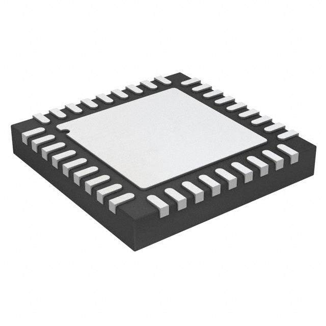
| 描述 | IC MIXER 500MHZ UP CONVRT 8SO射频混合器 LP VHF DBL-BAL W/OSC |
| 产品分类 | |
| 品牌 | NXP Semiconductors |
| 产品手册 | |
| 产品图片 |
|
| rohs | 符合RoHS无铅 / 符合限制有害物质指令(RoHS)规范要求 |
| 产品系列 | RF集成电路,射频混合器,NXP Semiconductors SA612AD/01,112SA612 |
| 数据手册 | |
| 产品型号 | SA612AD/01,112 |
| PCN封装 | |
| RF类型 | 手机,HF,VHF |
| 产品培训模块 | http://www.digikey.cn/PTM/IndividualPTM.page?site=cn&lang=zhs&ptm=19826http://www.digikey.cn/PTM/IndividualPTM.page?site=cn&lang=zhs&ptm=30627 |
| 产品目录页面 | |
| 产品种类 | 射频混合器 |
| 供应商器件封装 | 8-SO |
| 其它名称 | 568-1204-5 |
| 包装 | 管件 |
| 商标 | NXP Semiconductors |
| 噪声系数 | 5dB |
| 增益 | 17dB |
| 安装风格 | SMD/SMT |
| 封装 | Tube |
| 封装/外壳 | 8-SOIC(0.154",3.90mm 宽) |
| 封装/箱体 | SO-8 |
| 工作电源电压 | 6 V |
| 工厂包装数量 | 2000 |
| 标准包装 | 100 |
| 混频器数 | 1 |
| 特色产品 | http://www.digikey.cn/product-highlights/zh/sa6xx-series-rfif-building-blocks/52826 |
| 电压-电源 | 4.5 V ~ 8 V |
| 电流-电源 | 2.4mA |
| 电源电流 | 2.4 mA |
| 类型 | Mixers |
| 辅助属性 | 升频器 |
| 零件号别名 | SA612AD/01 |
| 频率 | 500MHz |


- 商务部:美国ITC正式对集成电路等产品启动337调查
- 曝三星4nm工艺存在良率问题 高通将骁龙8 Gen1或转产台积电
- 太阳诱电将投资9.5亿元在常州建新厂生产MLCC 预计2023年完工
- 英特尔发布欧洲新工厂建设计划 深化IDM 2.0 战略
- 台积电先进制程称霸业界 有大客户加持明年业绩稳了
- 达到5530亿美元!SIA预计今年全球半导体销售额将创下新高
- 英特尔拟将自动驾驶子公司Mobileye上市 估值或超500亿美元
- 三星加码芯片和SET,合并消费电子和移动部门,撤换高东真等 CEO
- 三星电子宣布重大人事变动 还合并消费电子和移动部门
- 海关总署:前11个月进口集成电路产品价值2.52万亿元 增长14.8%


PDF Datasheet 数据手册内容提取
SA612A Double-balanced mixer and oscillator Rev. 3 — 4 June 2014 Product data sheet 1. General description The SA612A is a low-power VHF monolithic double-balanced mixer with on-board oscillator and voltage regulator. It is intended for low cost, low-power communication systems with signal frequencies to 500MHz and local oscillator frequencies as high as 200MHz. The mixer is a ‘Gilbert cell’ multiplier configuration that provides gain of 14dB or more at 45MHz. The oscillator can be configured for a crystal, a tuned tank operation, or as a buffer for an external LO. Noise figure at 45MHz is typically below 6dB and makes the device well-suited for high-performance cordless phone/cellular radio. The low power consumption makes the SA612A excellent for battery-operated equipment. Networking and other communications products can benefit from very low radiated energy levels within systems. The SA612A is available in an 8-lead SO (surface-mounted miniature package). 2. Features and benefits Low current consumption Low cost Operation to 500MHz Low radiated energy Low external parts count; suitable for crystal/ceramic filter Excellent sensitivity, gain, and noise figure 3. Applications Cordless telephone Portable radio VHF transceivers RF data links Sonobuoys Communications receivers Broadband LANs HF and VHF frequency conversion Cellular radio mixer/oscillator
SA612A NXP Semiconductors Double-balanced mixer and oscillator 4. Ordering information Table 1. Ordering info rmation Type number Topside Package marking Name Description Version SA612AD/01 SA612A SO8 plastic small outline package; 8leads; bodywidth3.9mm SOT96-1 4.1 Ordering options Table 2. Ordering opt ions Type number Orderable Package Packing method Minimum Temperature partnumber order quantity SA612AD/01 SA612AD/01,112 SO8 Standard marking 2000 T =40C to +85C amb *IC’s tube - DSC bulk pack SA612AD/01,118 SO8 Reel 13” Q1/T1 2500 T =40C to +85C amb *Standard mark SMD 5. Block diagram E B B _ _ _ CC SC SC UT V O O O 8 7 6 5 E B VOLTAGE REGULATOR OSCILLATOR 1 2 3 4 A B D A _ _ N _ IN IN G UT O aaa-013372 Fig 1. Block diagram SA612A All information provided in this document is subject to legal disclaimers. © NXP Semiconductors N.V. 2014. All rights reserved. Product data sheet Rev. 3 — 4 June 2014 2 of 19
SA612A NXP Semiconductors Double-balanced mixer and oscillator 6. Pinning information 6.1 Pinning SA612AD/01 IN_A 1 8 VCC IN_B 2 7 OSC_E GND 3 6 OSC_B OUT_A 4 5 OUT_B aaa-013371 Fig 2. Pin configuration for SO8 6.2 Pin description Table 3. Pin description Symbol Pin Description IN_A 1 RF input A IN_B 2 RF input B GND 3 ground OUT_A 4 mixer output A OUT_B 5 mixer output B OSC_B 6 oscillator input (base) OSC_E 7 oscillator output (emitter) V 8 supply voltage CC SA612A All information provided in this document is subject to legal disclaimers. © NXP Semiconductors N.V. 2014. All rights reserved. Product data sheet Rev. 3 — 4 June 2014 3 of 19
SA612A NXP Semiconductors Double-balanced mixer and oscillator 7. Functional description The SA612A is a Gilbert cell, an oscillator/buffer, and a temperature-compensated bias network as shown in Figure3. The Gilbert cell is a differential amplifier (IN_A and IN_B pins) that drives a balanced switching cell. The differential input stage provides gain and determines the noise figure and signal handling performance of the system. 18 kΩ 1.5 kΩ 1.5 kΩ buffer 6 4 5 7 25 kΩ BIAS BIAS 2 1 BIAS 1.5 kΩ 1.5 kΩ 3 GND aaa-013205 Fig 3. Equivalent circuit The SA612A is designed for optimum low-power performance. When used with the SA614A as a 45MHz cordless phone/cellular radio second IF and demodulator, the SA612A is capable of receiving 119dBm signals with a 12dB S/N ratio. Third-order intercept is typically 15dBm (that is approximately +5dBm output intercept because of the RF gain). The system designer must be cognizant of this large signal limitation. When designing LANs or other closed systems where transmission levels are high, and small-signal or signal-to-noise issues are not critical, the input to the SA612A should be appropriately scaled. Besides excellent low-power performance well into VHF, the SA612A is flexible. The input, output and oscillator ports support various configurations provided the designer understands certain constraints, which are explained here. The RF inputs (IN_A and IN_B pins) are biased internally. They are symmetrical. The equivalent AC input impedance is approximately 1.5k3pF through 50MHz. IN_A and IN_B pins can be used interchangeably, but they should not be DC biased externally. Figure4 shows three typical input configurations. SA612A All information provided in this document is subject to legal disclaimers. © NXP Semiconductors N.V. 2014. All rights reserved. Product data sheet Rev. 3 — 4 June 2014 4 of 19
SA612A NXP Semiconductors Double-balanced mixer and oscillator SA612A SA612A SA612A 1 2 1 2 1 2 input aaa-013374 aaa-013375 aaa-013376 a. Single-ended b. Balanced input c. Single-ended tunedinput (forattenuation of untuned input second-order products) Fig 4. Input configuration The mixer outputs (OUT_A and OUT_B pins) are also internally biased. Each output is connected to the internal positive supply by a 1.5k resistor. This permits direct output termination yet allows for balanced output as well. Figure5 shows three single-ended output configurations and a balanced output. CFU455 or equivalent 12 pF Ctune(xtal) 5 5 Filter: K&L 38780 or equivalent SA612A SA612A Ctune(xtal) matches 3.5 kΩ to next stage 4 4 aaa-013377 aaa-013378 a. Single-ended ceramic filter b. Single-ended crystal filter 5 5 SA612A SA612A 4 4 aaa-013379 aaa-013380 c. Single-ended IFT d. Balanced output Fig 5. Output configuration SA612A All information provided in this document is subject to legal disclaimers. © NXP Semiconductors N.V. 2014. All rights reserved. Product data sheet Rev. 3 — 4 June 2014 5 of 19
SA612A NXP Semiconductors Double-balanced mixer and oscillator The oscillator can sustain oscillation beyond 200MHz in crystal or tuned tank configurations. The upper limit of operation is determined by tank ‘Q’ and required drive levels. The higher the ‘Q’ of the tank or the smaller the required drive, the higher the permissible oscillation frequency. If the required LO is beyond oscillation limits, or the system calls for an external LO, the external signal can be injected at OSC_B (pin6) through a DC blocking capacitor. External LO should be 200mV (peak-to-peak) minimum up to 300mV (peak-to-peak) maximum. Figure6 shows several proven oscillator circuits. Figure6a is appropriate for cordless phones or cellular radio. As shown, an overtone mode of operation is utilized. Capacitor C3 and inductor L1 act as a fundamental trap. In fundamental mode oscillation, the trap is omitted. C2 L1 C3 XTAL C1 8 7 6 5 8 7 6 5 8 7 6 5 SA612A SA612A SA612A 1 2 3 4 1 2 3 4 1 2 3 4 aaa-013381 aaa-013382 aaa-013383 a. Colpitts crystal b. Colpitts L/C tank c. Hartley L/C tank oscillator oscillator oscillator (overtonemode) Fig 6. Oscillator circuits Figure7 shows a Colpitts varactor tuned tank oscillator suitable for synthesizer-controlled applications. It is important to buffer the output of this circuit to assure that switching spikes from the first counter or prescaler do not end up in the oscillator spectrum. The dual-gate MOSFET provides optimum isolation with low current. The FET offers good isolation, simplicity, and low current, while the bipolar transistors provide the simple solution for non-critical applications. The resistive divider in the emitter-follower circuit should be chosen to provide the minimum input signal that assures correct system operation. SA612A All information provided in this document is subject to legal disclaimers. © NXP Semiconductors N.V. 2014. All rights reserved. Product data sheet Rev. 3 — 4 June 2014 6 of 19
SA612A NXP Semiconductors Double-balanced mixer and oscillator 5.5 μH +6 V 10 nF 10 μF 0.1 μF 1 8 2 7 to buffer SA612A 7 pF 10 pF 3 6 1000 pF DC control voltage 4 5 from synthesizer 1000 pF MV2105 0.06 μH or equivalent 0.01 μF 100 kΩ 2 kΩ 0.01 pF 2N918 3SK126 2 pF to synthesizer 2N5484 100 kΩ 330 Ω 0.01 μF to synthesizer 100 kΩ 1.0 nF aaa-013384 Fig 7. Colpitts oscillator suitable for synthesizer applications and typical buffers 8. Application design-in information 22 pF 0.5 μH to 1.3 μH 1 nF 44.545 MHz third overtone crystal 5.5 μH 5.6 pF VCC 6.8 μF 100 nF 10 nF 8 7 6 5 SA612A 1 2 3 4 SFG455A3 or equivalent 455 kHz output 47 pF 0.209 μH 45 MHz to RF input 220 pF 0.283 μH 100 nF aaa-013385 Fig 8. Typical application for cordless/cellular radio SA612A All information provided in this document is subject to legal disclaimers. © NXP Semiconductors N.V. 2014. All rights reserved. Product data sheet Rev. 3 — 4 June 2014 7 of 19
SA612A NXP Semiconductors Double-balanced mixer and oscillator 9. Limiting values Table 4. Limiting values In accordance with the Absolute Maximum Rating System (IEC 60134). Symbol Parameter Conditions Min Max Unit V supply voltage - 9 V CC T storage temperature 65 +150 C stg T ambient temperature operating 40 +85 C amb 10. Static characteristics Table 5. Static characteristics T =25C; V =+6V; unless specified otherwise. Refer to Figure15. amb CC Symbol Parameter Conditions Min Typ Max Unit V supply voltage 4.5 - 8.0 V CC I supply current - 2.4 3.0 mA CC 11. Dynamic characteristics Table 6. Dynamic characteristics T =25C; V =+6V; unless specified otherwise. Refer to Figure15. amb CC Symbol Parameter Conditions Min Typ Max Unit f input frequency - 500 - MHz i f oscillator frequency - 200 - MHz osc NF noise figure at 45MHz - 5.0 - dB IP3 input third-order RFinput=45dBm; - 13 - dBm i intercept point RF1=45.0MHz; RF2=45.06MHz G conversion gain at 45MHz 14 17 - dB conv R RF input resistance 1.5 - - k i(RF) C RF input capacitance - 3 - pF i(RF) R mixer output resistance OUT_A, OUT_B pins - 1.5 - k o(mix) SA612A All information provided in this document is subject to legal disclaimers. © NXP Semiconductors N.V. 2014. All rights reserved. Product data sheet Rev. 3 — 4 June 2014 8 of 19
SA612A NXP Semiconductors Double-balanced mixer and oscillator 12. Performance curves aaa-013241 aaa-013242 3.5 20.0 (ImCAC) Gconv VCC = 8.5 V (dB) 3.0 18.0 VCC = 8.5 V 6.0 V 2.5 6.0 V 4.5 V 4.5 V 16.0 2.0 1.5 14.0 −40 −20 0 20 40 60 80 90 −40 −20 0 20 40 60 80 90 Tamb (°C) Tamb (°C) Fig 9. Supply current versus temperature Fig 10. Conversion gain versus temperature aaa-013243 aaa-013244 −10.0 6.0 NF IP3i (dB) (dBm) 5.5 −12.0 VCC = 8.5 V 6.0 V 5.0 4.5 V −14.0 4.5 −16.0 4.0 −40 −20 0 20 40 60 80 90 −40 −20 0 20 40 60 80 90 Tamb (°C) Tamb (°C) Fig 11. Third-order intercept point versus temperature Fig 12. Noise Figure versus temperature aaa-013245 aaa-013246 40 −10 IF output power third-order product (dIPB3mi) (dBm) −12 0 −14 fund. product −40 −16 −80 −18 −80 −60 −40 −20 0 20 4 6 8 10 RF input level (dBm) VCC (V) RF1 = 45MHz; IF = 455kHz; RF2 = 45.06MHz Fig 13. Third-order intercept and compression Fig 14. Input third-order intercept point versus supplyvoltage SA612A All information provided in this document is subject to legal disclaimers. © NXP Semiconductors N.V. 2014. All rights reserved. Product data sheet Rev. 3 — 4 June 2014 9 of 19
SA612A NXP Semiconductors Double-balanced mixer and oscillator 13. Test information 22 pF 0.5 μH to 1.3 μH 1 nF 44.545 MHz third overtone crystal 5.5 μH 10 pF VCC 6.8 μF 100 nF 10 nF 8 7 6 5 330 pF 455 kHz SA612A 303to μH IF output 560 pF 765 μH 100 nF 1 2 3 4 47 pF 0.209 μH 45 MHz to RF input 220 pF 0.283 μH 100 nF aaa-013373 Fig 15. Test configuration SA612A All information provided in this document is subject to legal disclaimers. © NXP Semiconductors N.V. 2014. All rights reserved. Product data sheet Rev. 3 — 4 June 2014 10 of 19
SA612A NXP Semiconductors Double-balanced mixer and oscillator 14. Package outline (cid:54)(cid:50)(cid:27)(cid:29)(cid:3)(cid:83)(cid:79)(cid:68)(cid:86)(cid:87)(cid:76)(cid:70)(cid:3)(cid:86)(cid:80)(cid:68)(cid:79)(cid:79)(cid:3)(cid:82)(cid:88)(cid:87)(cid:79)(cid:76)(cid:81)(cid:72)(cid:3)(cid:83)(cid:68)(cid:70)(cid:78)(cid:68)(cid:74)(cid:72)(cid:30)(cid:3)(cid:27)(cid:3)(cid:79)(cid:72)(cid:68)(cid:71)(cid:86)(cid:30)(cid:3)(cid:69)(cid:82)(cid:71)(cid:92)(cid:3)(cid:90)(cid:76)(cid:71)(cid:87)(cid:75)(cid:3)(cid:22)(cid:17)(cid:28)(cid:3)(cid:80)(cid:80)(cid:3) (cid:54)(cid:50)(cid:55)(cid:28)(cid:25)(cid:16)(cid:20)(cid:3) (cid:39)(cid:3) (cid:40)(cid:3) (cid:36)(cid:3) (cid:59)(cid:3) (cid:70)(cid:3) (cid:92)(cid:3) (cid:43)(cid:3)(cid:40)(cid:3) (cid:89)(cid:3)(cid:48)(cid:3) (cid:36)(cid:3) (cid:61)(cid:3) (cid:27)(cid:3) (cid:24)(cid:3) (cid:52)(cid:3) (cid:36)(cid:3)(cid:21)(cid:3)(cid:36)(cid:3)(cid:20)(cid:3) (cid:11)(cid:36)(cid:3)(cid:22)(cid:3)(cid:3)(cid:12)(cid:3) (cid:36)(cid:3) (cid:83)(cid:76)(cid:81)(cid:3)(cid:20)(cid:3)(cid:76)(cid:81)(cid:71)(cid:72)(cid:91)(cid:3) (cid:537)(cid:3) (cid:47)(cid:3)(cid:83)(cid:3) (cid:20)(cid:3) (cid:23)(cid:3) (cid:47)(cid:3) (cid:72)(cid:3) (cid:90)(cid:3)(cid:48)(cid:3) (cid:71)(cid:72)(cid:87)(cid:68)(cid:76)(cid:79)(cid:3)(cid:59)(cid:3) (cid:69)(cid:3)(cid:83)(cid:3) (cid:19)(cid:3) (cid:21)(cid:17)(cid:24)(cid:3) (cid:24)(cid:3)(cid:80)(cid:80)(cid:3) (cid:86)(cid:70)(cid:68)(cid:79)(cid:72)(cid:3) (cid:39)(cid:44)(cid:48)(cid:40)(cid:49)(cid:54)(cid:44)(cid:50)(cid:49)(cid:54)(cid:3)(cid:11)(cid:76)(cid:81)(cid:70)(cid:75)(cid:3)(cid:71)(cid:76)(cid:80)(cid:72)(cid:81)(cid:86)(cid:76)(cid:82)(cid:81)(cid:86)(cid:3)(cid:68)(cid:85)(cid:72)(cid:3)(cid:71)(cid:72)(cid:85)(cid:76)(cid:89)(cid:72)(cid:71)(cid:3)(cid:73)(cid:85)(cid:82)(cid:80)(cid:3)(cid:87)(cid:75)(cid:72)(cid:3)(cid:82)(cid:85)(cid:76)(cid:74)(cid:76)(cid:81)(cid:68)(cid:79)(cid:3)(cid:80)(cid:80)(cid:3)(cid:71)(cid:76)(cid:80)(cid:72)(cid:81)(cid:86)(cid:76)(cid:82)(cid:81)(cid:86)(cid:12)(cid:3) (cid:56)(cid:49)(cid:44)(cid:55)(cid:3) (cid:80)(cid:36)(cid:68)(cid:91)(cid:3)(cid:17)(cid:3) (cid:36)(cid:3)(cid:20)(cid:3) (cid:36)(cid:3)(cid:21)(cid:3) (cid:36)(cid:3)(cid:22)(cid:3) (cid:69)(cid:3)(cid:83)(cid:3) (cid:70)(cid:3) (cid:39)(cid:3)(cid:11)(cid:20)(cid:12)(cid:3) (cid:40)(cid:3)(cid:11)(cid:21)(cid:12)(cid:3) (cid:72)(cid:3) (cid:43)(cid:3)(cid:40)(cid:3) (cid:47)(cid:3) (cid:47)(cid:3)(cid:83)(cid:3) (cid:52)(cid:3) (cid:89)(cid:3) (cid:90)(cid:3) (cid:92)(cid:3) (cid:61)(cid:3)(cid:11)(cid:20)(cid:12)(cid:3) (cid:537)(cid:3) (cid:19)(cid:17)(cid:21)(cid:24)(cid:3) (cid:20)(cid:17)(cid:23)(cid:24)(cid:3) (cid:19)(cid:17)(cid:23)(cid:28)(cid:3) (cid:19)(cid:17)(cid:21)(cid:24)(cid:3) (cid:24)(cid:17)(cid:19)(cid:3) (cid:23)(cid:17)(cid:19)(cid:3) (cid:25)(cid:17)(cid:21)(cid:3) (cid:20)(cid:17)(cid:19)(cid:3) (cid:19)(cid:17)(cid:26)(cid:3) (cid:19)(cid:17)(cid:26)(cid:3) (cid:80)(cid:80)(cid:3) (cid:20)(cid:17)(cid:26)(cid:24)(cid:3) (cid:19)(cid:17)(cid:21)(cid:24)(cid:3) (cid:20)(cid:17)(cid:21)(cid:26)(cid:3) (cid:20)(cid:17)(cid:19)(cid:24)(cid:3) (cid:19)(cid:17)(cid:21)(cid:24)(cid:3) (cid:19)(cid:17)(cid:21)(cid:24)(cid:3) (cid:19)(cid:17)(cid:20)(cid:3) (cid:19)(cid:17)(cid:20)(cid:19)(cid:3) (cid:20)(cid:17)(cid:21)(cid:24)(cid:3) (cid:19)(cid:17)(cid:22)(cid:25)(cid:3) (cid:19)(cid:17)(cid:20)(cid:28)(cid:3) (cid:23)(cid:17)(cid:27)(cid:3) (cid:22)(cid:17)(cid:27)(cid:3) (cid:24)(cid:17)(cid:27)(cid:3) (cid:19)(cid:17)(cid:23)(cid:3) (cid:19)(cid:17)(cid:25)(cid:3) (cid:19)(cid:17)(cid:22)(cid:3) (cid:27)(cid:3)(cid:82)(cid:3) (cid:19)(cid:17)(cid:19)(cid:20)(cid:19)(cid:3) (cid:19)(cid:17)(cid:19)(cid:24)(cid:26)(cid:3) (cid:19)(cid:17)(cid:19)(cid:20)(cid:28)(cid:3)(cid:19)(cid:17)(cid:19)(cid:20)(cid:19)(cid:19)(cid:3) (cid:19)(cid:17)(cid:21)(cid:19)(cid:3) (cid:19)(cid:17)(cid:20)(cid:25)(cid:3) (cid:19)(cid:17)(cid:21)(cid:23)(cid:23)(cid:3) (cid:19)(cid:17)(cid:19)(cid:22)(cid:28)(cid:3) (cid:19)(cid:17)(cid:19)(cid:21)(cid:27)(cid:3) (cid:19)(cid:17)(cid:19)(cid:21)(cid:27)(cid:3) (cid:19)(cid:3)(cid:82)(cid:3) (cid:76)(cid:81)(cid:70)(cid:75)(cid:72)(cid:86)(cid:3) (cid:19)(cid:17)(cid:19)(cid:25)(cid:28)(cid:3) (cid:19)(cid:17)(cid:19)(cid:20)(cid:3) (cid:19)(cid:17)(cid:19)(cid:24)(cid:3) (cid:19)(cid:17)(cid:19)(cid:23)(cid:20)(cid:3) (cid:19)(cid:17)(cid:19)(cid:20)(cid:3) (cid:19)(cid:17)(cid:19)(cid:20)(cid:3) (cid:19)(cid:17)(cid:19)(cid:19)(cid:23)(cid:3) (cid:19)(cid:17)(cid:19)(cid:19)(cid:23)(cid:3) (cid:19)(cid:17)(cid:19)(cid:23)(cid:28)(cid:3) (cid:19)(cid:17)(cid:19)(cid:20)(cid:23)(cid:3)(cid:19)(cid:17)(cid:19)(cid:19)(cid:26)(cid:24)(cid:3) (cid:19)(cid:17)(cid:20)(cid:28)(cid:3) (cid:19)(cid:17)(cid:20)(cid:24)(cid:3) (cid:19)(cid:17)(cid:21)(cid:21)(cid:27)(cid:3) (cid:19)(cid:17)(cid:19)(cid:20)(cid:25)(cid:3) (cid:19)(cid:17)(cid:19)(cid:21)(cid:23)(cid:3) (cid:19)(cid:17)(cid:19)(cid:20)(cid:21)(cid:3) (cid:49)(cid:82)(cid:87)(cid:72)(cid:86)(cid:3) (cid:20)(cid:17)(cid:3)(cid:51)(cid:79)(cid:68)(cid:86)(cid:87)(cid:76)(cid:70)(cid:3)(cid:82)(cid:85)(cid:3)(cid:80)(cid:72)(cid:87)(cid:68)(cid:79)(cid:3)(cid:83)(cid:85)(cid:82)(cid:87)(cid:85)(cid:88)(cid:86)(cid:76)(cid:82)(cid:81)(cid:86)(cid:3)(cid:82)(cid:73)(cid:3)(cid:19)(cid:17)(cid:20)(cid:24)(cid:3)(cid:80)(cid:80)(cid:3)(cid:11)(cid:19)(cid:17)(cid:19)(cid:19)(cid:25)(cid:3)(cid:76)(cid:81)(cid:70)(cid:75)(cid:12)(cid:3)(cid:80)(cid:68)(cid:91)(cid:76)(cid:80)(cid:88)(cid:80)(cid:3)(cid:83)(cid:72)(cid:85)(cid:3)(cid:86)(cid:76)(cid:71)(cid:72)(cid:3)(cid:68)(cid:85)(cid:72)(cid:3)(cid:81)(cid:82)(cid:87)(cid:3)(cid:76)(cid:81)(cid:70)(cid:79)(cid:88)(cid:71)(cid:72)(cid:71)(cid:17)(cid:3) (cid:21)(cid:17)(cid:3)(cid:51)(cid:79)(cid:68)(cid:86)(cid:87)(cid:76)(cid:70)(cid:3)(cid:82)(cid:85)(cid:3)(cid:80)(cid:72)(cid:87)(cid:68)(cid:79)(cid:3)(cid:83)(cid:85)(cid:82)(cid:87)(cid:85)(cid:88)(cid:86)(cid:76)(cid:82)(cid:81)(cid:86)(cid:3)(cid:82)(cid:73)(cid:3)(cid:19)(cid:17)(cid:21)(cid:24)(cid:3)(cid:80)(cid:80)(cid:3)(cid:11)(cid:19)(cid:17)(cid:19)(cid:20)(cid:3)(cid:76)(cid:81)(cid:70)(cid:75)(cid:12)(cid:3)(cid:80)(cid:68)(cid:91)(cid:76)(cid:80)(cid:88)(cid:80)(cid:3)(cid:83)(cid:72)(cid:85)(cid:3)(cid:86)(cid:76)(cid:71)(cid:72)(cid:3)(cid:68)(cid:85)(cid:72)(cid:3)(cid:81)(cid:82)(cid:87)(cid:3)(cid:76)(cid:81)(cid:70)(cid:79)(cid:88)(cid:71)(cid:72)(cid:71)(cid:17)(cid:3)(cid:3) (cid:50)(cid:56)(cid:55)(cid:47)(cid:44)(cid:49)(cid:40)(cid:3) (cid:3)(cid:53)(cid:40)(cid:41)(cid:40)(cid:53)(cid:40)(cid:49)(cid:38)(cid:40)(cid:54)(cid:3) (cid:40)(cid:56)(cid:53)(cid:50)(cid:51)(cid:40)(cid:36)(cid:49)(cid:3) (cid:44)(cid:54)(cid:54)(cid:56)(cid:40)(cid:3)(cid:39)(cid:36)(cid:55)(cid:40)(cid:3) (cid:57)(cid:40)(cid:53)(cid:54)(cid:44)(cid:50)(cid:49)(cid:3) (cid:3)(cid:44)(cid:40)(cid:38)(cid:3) (cid:3)(cid:45)(cid:40)(cid:39)(cid:40)(cid:38)(cid:3) (cid:3)(cid:45)(cid:40)(cid:44)(cid:55)(cid:36)(cid:3) (cid:51)(cid:53)(cid:50)(cid:45)(cid:40)(cid:38)(cid:55)(cid:44)(cid:50)(cid:49)(cid:3) (cid:28)(cid:28)(cid:16)(cid:20)(cid:21)(cid:16)(cid:21)(cid:26)(cid:3) (cid:3)(cid:54)(cid:50)(cid:55)(cid:28)(cid:25)(cid:16)(cid:20)(cid:3) (cid:19)(cid:26)(cid:25)(cid:40)(cid:19)(cid:22)(cid:3) (cid:3)(cid:48)(cid:54)(cid:16)(cid:19)(cid:20)(cid:21)(cid:3) (cid:19)(cid:22)(cid:16)(cid:19)(cid:21)(cid:16)(cid:20)(cid:27)(cid:3) Fig 16. Package outline SOT96-1 (SO8) SA612A All information provided in this document is subject to legal disclaimers. © NXP Semiconductors N.V. 2014. All rights reserved. Product data sheet Rev. 3 — 4 June 2014 11 of 19
SA612A NXP Semiconductors Double-balanced mixer and oscillator 15. Soldering of SMD packages This text provides a very brief insight into a complex technology. A more in-depth account of soldering ICs can be found in Application Note AN10365 “Surface mount reflow soldering description”. 15.1 Introduction to soldering Soldering is one of the most common methods through which packages are attached to Printed Circuit Boards (PCBs), to form electrical circuits. The soldered joint provides both the mechanical and the electrical connection. There is no single soldering method that is ideal for all IC packages. Wave soldering is often preferred when through-hole and Surface Mount Devices (SMDs) are mixed on one printed wiring board; however, it is not suitable for fine pitch SMDs. Reflow soldering is ideal for the small pitches and high densities that come with increased miniaturization. 15.2 Wave and reflow soldering Wave soldering is a joining technology in which the joints are made by solder coming from a standing wave of liquid solder. The wave soldering process is suitable for the following: • Through-hole components • Leaded or leadless SMDs, which are glued to the surface of the printed circuit board Not all SMDs can be wave soldered. Packages with solder balls, and some leadless packages which have solder lands underneath the body, cannot be wave soldered. Also, leaded SMDs with leads having a pitch smaller than ~0.6mm cannot be wave soldered, due to an increased probability of bridging. The reflow soldering process involves applying solder paste to a board, followed by component placement and exposure to a temperature profile. Leaded packages, packages with solder balls, and leadless packages are all reflow solderable. Key characteristics in both wave and reflow soldering are: • Board specifications, including the board finish, solder masks and vias • Package footprints, including solder thieves and orientation • The moisture sensitivity level of the packages • Package placement • Inspection and repair • Lead-free soldering versus SnPb soldering 15.3 Wave soldering Key characteristics in wave soldering are: • Process issues, such as application of adhesive and flux, clinching of leads, board transport, the solder wave parameters, and the time during which components are exposed to the wave • Solder bath specifications, including temperature and impurities SA612A All information provided in this document is subject to legal disclaimers. © NXP Semiconductors N.V. 2014. All rights reserved. Product data sheet Rev. 3 — 4 June 2014 12 of 19
SA612A NXP Semiconductors Double-balanced mixer and oscillator 15.4 Reflow soldering Key characteristics in reflow soldering are: • Lead-free versus SnPb soldering; note that a lead-free reflow process usually leads to higher minimum peak temperatures (see Figure17) than a SnPb process, thus reducing the process window • Solder paste printing issues including smearing, release, and adjusting the process window for a mix of large and small components on one board • Reflow temperature profile; this profile includes preheat, reflow (in which the board is heated to the peak temperature) and cooling down. It is imperative that the peak temperature is high enough for the solder to make reliable solder joints (a solder paste characteristic). In addition, the peak temperature must be low enough that the packages and/or boards are not damaged. The peak temperature of the package depends on package thickness and volume and is classified in accordance with Table7 and8 Table 7. SnPb eutectic process (from J-STD-020D) Package thickness (mm) Package reflow temperature (C) Volume (mm3) < 350 350 < 2.5 235 220 2.5 220 220 Table 8. Lead-free process (from J-STD-020D) Package thickness (mm) Package reflow temperature (C) Volume (mm3) < 350 350 to 2000 > 2000 < 1.6 260 260 260 1.6 to 2.5 260 250 245 > 2.5 250 245 245 Moisture sensitivity precautions, as indicated on the packing, must be respected at all times. Studies have shown that small packages reach higher temperatures during reflow soldering, see Figure17. SA612A All information provided in this document is subject to legal disclaimers. © NXP Semiconductors N.V. 2014. All rights reserved. Product data sheet Rev. 3 — 4 June 2014 13 of 19
SA612A NXP Semiconductors Double-balanced mixer and oscillator maximum peak temperature = MSL limit, damage level temperature minimum peak temperature = minimum soldering temperature peak temperature time 001aac844 MSL: Moisture Sensitivity Level Fig 17. Temperature profiles for large and small components For further information on temperature profiles, refer to Application Note AN10365 “Surface mount reflow soldering description”. 16. Soldering: PCB footprints (cid:24)(cid:17)(cid:24)(cid:19) (cid:19)(cid:17)(cid:25)(cid:19)(cid:3)(cid:11)(cid:27)(cid:238)(cid:12) (cid:20)(cid:17)(cid:22)(cid:19) (cid:23)(cid:17)(cid:19)(cid:19) (cid:25)(cid:17)(cid:25)(cid:19) (cid:26)(cid:17)(cid:19)(cid:19) (cid:20)(cid:17)(cid:21)(cid:26)(cid:3)(cid:11)(cid:25)(cid:238)(cid:12) (cid:86)(cid:82)(cid:79)(cid:71)(cid:72)(cid:85)(cid:3)(cid:79)(cid:68)(cid:81)(cid:71)(cid:86) (cid:82)(cid:70)(cid:70)(cid:88)(cid:83)(cid:76)(cid:72)(cid:71)(cid:3)(cid:68)(cid:85)(cid:72)(cid:68) (cid:83)(cid:79)(cid:68)(cid:70)(cid:72)(cid:80)(cid:72)(cid:81)(cid:87)(cid:3)(cid:68)(cid:70)(cid:70)(cid:88)(cid:85)(cid:68)(cid:70)(cid:92)(cid:3)(cid:147)(cid:3)(cid:19)(cid:17)(cid:21)(cid:24) (cid:39)(cid:76)(cid:80)(cid:72)(cid:81)(cid:86)(cid:76)(cid:82)(cid:81)(cid:86)(cid:3)(cid:76)(cid:81)(cid:3)(cid:80)(cid:80) (cid:86)(cid:82)(cid:87)(cid:19)(cid:28)(cid:25)(cid:16)(cid:20)(cid:66)(cid:73)(cid:85) Fig 18. PCB footprint for SOT96-1 (SO8); reflow soldering SA612A All information provided in this document is subject to legal disclaimers. © NXP Semiconductors N.V. 2014. All rights reserved. Product data sheet Rev. 3 — 4 June 2014 14 of 19
SA612A NXP Semiconductors Double-balanced mixer and oscillator (cid:20)(cid:17)(cid:21)(cid:19)(cid:3)(cid:11)(cid:21)(cid:238)(cid:12) (cid:19)(cid:17)(cid:25)(cid:19)(cid:3)(cid:11)(cid:25)(cid:238)(cid:12) (cid:19)(cid:17)(cid:22)(cid:3)(cid:11)(cid:21)(cid:238)(cid:12) (cid:72)(cid:81)(cid:79)(cid:68)(cid:85)(cid:74)(cid:72)(cid:71)(cid:3)(cid:86)(cid:82)(cid:79)(cid:71)(cid:72)(cid:85)(cid:3)(cid:79)(cid:68)(cid:81)(cid:71) (cid:20)(cid:17)(cid:22)(cid:19) (cid:23)(cid:17)(cid:19)(cid:19) (cid:25)(cid:17)(cid:25)(cid:19) (cid:26)(cid:17)(cid:19)(cid:19) (cid:20)(cid:17)(cid:21)(cid:26)(cid:3)(cid:11)(cid:25)(cid:238)(cid:12) (cid:24)(cid:17)(cid:24)(cid:19) (cid:69)(cid:82)(cid:68)(cid:85)(cid:71)(cid:3)(cid:71)(cid:76)(cid:85)(cid:72)(cid:70)(cid:87)(cid:76)(cid:82)(cid:81) (cid:86)(cid:82)(cid:79)(cid:71)(cid:72)(cid:85)(cid:3)(cid:79)(cid:68)(cid:81)(cid:71)(cid:86) (cid:86)(cid:82)(cid:79)(cid:71)(cid:72)(cid:85)(cid:3)(cid:85)(cid:72)(cid:86)(cid:76)(cid:86)(cid:87) (cid:82)(cid:70)(cid:70)(cid:88)(cid:83)(cid:76)(cid:72)(cid:71)(cid:3)(cid:68)(cid:85)(cid:72)(cid:68) (cid:83)(cid:79)(cid:68)(cid:70)(cid:72)(cid:80)(cid:72)(cid:81)(cid:87)(cid:3)(cid:68)(cid:70)(cid:70)(cid:88)(cid:85)(cid:85)(cid:68)(cid:70)(cid:92)(cid:3)(cid:147)(cid:3)(cid:19)(cid:17)(cid:21)(cid:24) (cid:39)(cid:76)(cid:80)(cid:72)(cid:81)(cid:86)(cid:76)(cid:82)(cid:81)(cid:86)(cid:3)(cid:76)(cid:81)(cid:3)(cid:80)(cid:80) (cid:86)(cid:82)(cid:87)(cid:19)(cid:28)(cid:25)(cid:16)(cid:20)(cid:66)(cid:73)(cid:90) Fig 19. PCB footprint for SOT96-1 (SO8); wave soldering 17. Abbreviations Table 9. Abbreviations Acronym Description FET Field-Effect Transistor HF High Frequency IF Intermediate Frequency LAN Local Area Network LO Local Oscillator MOSFET Metal-Oxide Semiconductor Field-Effect Transistor RF Radio Frequency S/N Signal-to-Noise ratio VHF Very High Frequency SA612A All information provided in this document is subject to legal disclaimers. © NXP Semiconductors N.V. 2014. All rights reserved. Product data sheet Rev. 3 — 4 June 2014 15 of 19
SA612A NXP Semiconductors Double-balanced mixer and oscillator 18. Revision history Table 10. Revision history Document ID Release date Data sheet status Change notice Supersedes SA612A v.3 20140604 Product data sheet - SA612A v.2 Modifications: • The format of this data sheet has been redesigned to comply with the new identity guidelines of NXP Semiconductors. • Legal texts have been adapted to the new company name where appropriate. • Section 1 “General description”, last sentence: deleted “8-lead dual in-line plastic package” • Table 1 “Ordering information”: – Type number SA612AN (DIP8 package, SOT97-1 package outline) is discontinued and removed from this data sheet – Type number changed from “SA612AD” to “SA612AD/01” • Added Section 4.1 “Ordering options” • Figure 2 “Pin configuration for SO8”, pin names are updated: – Pin 1: from “INPUT A” to “IN_A” – Pin 2: from “INPUT B” to “IN_B” – Pin 4: from “OUTPUT A” to “OUT_A” – Pin 5: from “OUTPUT B” to “OUT_B” – Pin 6: from “OSCILLATOR” to “OSC_B” – Pin 7: from “OSCILLATOR” to “OSC_E” • Added Section 6.2 “Pin description” • Section 7 “Functional description”, seventh paragraph, second sentence changed from “In this circuit, a third overtone parallel-mode crystal with approximately 5pF load capacitance should be specified.” to “As shown, an overtone mode of operation is utilized.” • Figure 7 “Colpitts oscillator suitable for synthesizer applications and typical buffers”: capacitor value corrected from “0.10 pF” to “10nF” (above pin 8) • Old table “AC/DC electrical characteristics” split into Table 5 “Static characteristics” and Table 6 “Dynamic characteristics” • Table 6 “Dynamic characteristics”, Conditions for IP3, input third-order intercept point, updated i from “at 45MHz; RF input = 45dBm” to “” • Package outline SOT97-1 (DIP8) is deleted • Added soldering information • Added Section 16 “Soldering: PCB footprints” • Added Section 17 “Abbreviations” SA612A v.2 19971107 Product specification 853-0391 18662 NE/SA612A v.1 NE/SA612A v.1 19900917 Product specification 853-0391 00446 - SA612A All information provided in this document is subject to legal disclaimers. © NXP Semiconductors N.V. 2014. All rights reserved. Product data sheet Rev. 3 — 4 June 2014 16 of 19
SA612A NXP Semiconductors Double-balanced mixer and oscillator 19. Legal information 19.1 Data sheet status Document status[1][2] Product status[3] Definition Objective [short] data sheet Development This document contains data from the objective specification for product development. Preliminary [short] data sheet Qualification This document contains data from the preliminary specification. Product [short] data sheet Production This document contains the product specification. [1] Please consult the most recently issued document before initiating or completing a design. [2] The term ‘short data sheet’ is explained in section “Definitions”. [3] The product status of device(s) described in this document may have changed since this document was published and may differ in case of multiple devices. The latest product status information is available on the Internet at URLhttp://www.nxp.com. 19.2 Definitions Suitability for use — NXP Semiconductors products are not designed, authorized or warranted to be suitable for use in life support, life-critical or safety-critical systems or equipment, nor in applications where failure or Draft — The document is a draft version only. The content is still under malfunction of an NXP Semiconductors product can reasonably be expected internal review and subject to formal approval, which may result in to result in personal injury, death or severe property or environmental modifications or additions. NXP Semiconductors does not give any damage. NXP Semiconductors and its suppliers accept no liability for representations or warranties as to the accuracy or completeness of inclusion and/or use of NXP Semiconductors products in such equipment or information included herein and shall have no liability for the consequences of applications and therefore such inclusion and/or use is at the customer’s own use of such information. risk. Short data sheet — A short data sheet is an extract from a full data sheet Applications — Applications that are described herein for any of these with the same product type number(s) and title. A short data sheet is intended products are for illustrative purposes only. NXP Semiconductors makes no for quick reference only and should not be relied upon to contain detailed and representation or warranty that such applications will be suitable for the full information. For detailed and full information see the relevant full data specified use without further testing or modification. sheet, which is available on request via the local NXP Semiconductors sales office. In case of any inconsistency or conflict with the short data sheet, the Customers are responsible for the design and operation of their applications full data sheet shall prevail. and products using NXP Semiconductors products, and NXP Semiconductors accepts no liability for any assistance with applications or customer product Product specification — The information and data provided in a Product design. It is customer’s sole responsibility to determine whether the NXP data sheet shall define the specification of the product as agreed between Semiconductors product is suitable and fit for the customer’s applications and NXP Semiconductors and its customer, unless NXP Semiconductors and products planned, as well as for the planned application and use of customer have explicitly agreed otherwise in writing. In no event however, customer’s third party customer(s). Customers should provide appropriate shall an agreement be valid in which the NXP Semiconductors product is design and operating safeguards to minimize the risks associated with their deemed to offer functions and qualities beyond those described in the applications and products. Product data sheet. NXP Semiconductors does not accept any liability related to any default, damage, costs or problem which is based on any weakness or default in the 19.3 Disclaimers customer’s applications or products, or the application or use by customer’s third party customer(s). Customer is responsible for doing all necessary testing for the customer’s applications and products using NXP Limited warranty and liability — Information in this document is believed to Semiconductors products in order to avoid a default of the applications and be accurate and reliable. However, NXP Semiconductors does not give any the products or of the application or use by customer’s third party representations or warranties, expressed or implied, as to the accuracy or customer(s). NXP does not accept any liability in this respect. completeness of such information and shall have no liability for the consequences of use of such information. NXP Semiconductors takes no Limiting values — Stress above one or more limiting values (as defined in responsibility for the content in this document if provided by an information the Absolute Maximum Ratings System of IEC60134) will cause permanent source outside of NXP Semiconductors. damage to the device. Limiting values are stress ratings only and (proper) operation of the device at these or any other conditions above those given in In no event shall NXP Semiconductors be liable for any indirect, incidental, the Recommended operating conditions section (if present) or the punitive, special or consequential damages (including - without limitation - lost Characteristics sections of this document is not warranted. Constant or profits, lost savings, business interruption, costs related to the removal or repeated exposure to limiting values will permanently and irreversibly affect replacement of any products or rework charges) whether or not such the quality and reliability of the device. damages are based on tort (including negligence), warranty, breach of contract or any other legal theory. Terms and conditions of commercial sale — NXP Semiconductors products are sold subject to the general terms and conditions of commercial Notwithstanding any damages that customer might incur for any reason whatsoever, NXP Semiconductors’ aggregate and cumulative liability towards sale, as published at http://www.nxp.com/profile/terms, unless otherwise customer for the products described herein shall be limited in accordance agreed in a valid written individual agreement. In case an individual with the Terms and conditions of commercial sale of NXP Semiconductors. agreement is concluded only the terms and conditions of the respective agreement shall apply. NXP Semiconductors hereby expressly objects to Right to make changes — NXP Semiconductors reserves the right to make applying the customer’s general terms and conditions with regard to the changes to information published in this document, including without purchase of NXP Semiconductors products by customer. limitation specifications and product descriptions, at any time and without notice. This document supersedes and replaces all information supplied prior No offer to sell or license — Nothing in this document may be interpreted or to the publication hereof. construed as an offer to sell products that is open for acceptance or the grant, conveyance or implication of any license under any copyrights, patents or other industrial or intellectual property rights. SA612A All information provided in this document is subject to legal disclaimers. © NXP Semiconductors N.V. 2014. All rights reserved. Product data sheet Rev. 3 — 4 June 2014 17 of 19
SA612A NXP Semiconductors Double-balanced mixer and oscillator Export control — This document as well as the item(s) described herein NXP Semiconductors’ specifications such use shall be solely at customer’s may be subject to export control regulations. Export might require a prior own risk, and (c) customer fully indemnifies NXP Semiconductors for any authorization from competent authorities. liability, damages or failed product claims resulting from customer design and use of the product for automotive applications beyond NXP Semiconductors’ Non-automotive qualified products — Unless this data sheet expressly standard warranty and NXP Semiconductors’ product specifications. states that this specific NXP Semiconductors product is automotive qualified, the product is not suitable for automotive use. It is neither qualified nor tested Translations — A non-English (translated) version of a document is for in accordance with automotive testing or application requirements. NXP reference only. The English version shall prevail in case of any discrepancy Semiconductors accepts no liability for inclusion and/or use of between the translated and English versions. non-automotive qualified products in automotive equipment or applications. In the event that customer uses the product for design-in and use in 19.4 Trademarks automotive applications to automotive specifications and standards, customer (a) shall use the product without NXP Semiconductors’ warranty of the Notice: All referenced brands, product names, service names and trademarks product for such automotive applications, use and specifications, and (b) are the property of their respective owners. whenever customer uses the product for automotive applications beyond 20. Contact information For more information, please visit: http://www.nxp.com For sales office addresses, please send an email to: salesaddresses@nxp.com SA612A All information provided in this document is subject to legal disclaimers. © NXP Semiconductors N.V. 2014. All rights reserved. Product data sheet Rev. 3 — 4 June 2014 18 of 19
SA612A NXP Semiconductors Double-balanced mixer and oscillator 21. Contents 1 General description. . . . . . . . . . . . . . . . . . . . . . 1 2 Features and benefits . . . . . . . . . . . . . . . . . . . . 1 3 Applications. . . . . . . . . . . . . . . . . . . . . . . . . . . . 1 4 Ordering information. . . . . . . . . . . . . . . . . . . . . 2 4.1 Ordering options. . . . . . . . . . . . . . . . . . . . . . . . 2 5 Block diagram . . . . . . . . . . . . . . . . . . . . . . . . . . 2 6 Pinning information. . . . . . . . . . . . . . . . . . . . . . 3 6.1 Pinning . . . . . . . . . . . . . . . . . . . . . . . . . . . . . . . 3 6.2 Pin description . . . . . . . . . . . . . . . . . . . . . . . . . 3 7 Functional description . . . . . . . . . . . . . . . . . . . 4 8 Application design-in information . . . . . . . . . . 7 9 Limiting values. . . . . . . . . . . . . . . . . . . . . . . . . . 8 10 Static characteristics. . . . . . . . . . . . . . . . . . . . . 8 11 Dynamic characteristics. . . . . . . . . . . . . . . . . . 8 12 Performance curves . . . . . . . . . . . . . . . . . . . . . 9 13 Test information. . . . . . . . . . . . . . . . . . . . . . . . 10 14 Package outline. . . . . . . . . . . . . . . . . . . . . . . . 11 15 Soldering of SMD packages . . . . . . . . . . . . . . 12 15.1 Introduction to soldering. . . . . . . . . . . . . . . . . 12 15.2 Wave and reflow soldering. . . . . . . . . . . . . . . 12 15.3 Wave soldering. . . . . . . . . . . . . . . . . . . . . . . . 12 15.4 Reflow soldering. . . . . . . . . . . . . . . . . . . . . . . 13 16 Soldering: PCB footprints. . . . . . . . . . . . . . . . 14 17 Abbreviations. . . . . . . . . . . . . . . . . . . . . . . . . . 15 18 Revision history. . . . . . . . . . . . . . . . . . . . . . . . 16 19 Legal information. . . . . . . . . . . . . . . . . . . . . . . 17 19.1 Data sheet status . . . . . . . . . . . . . . . . . . . . . . 17 19.2 Definitions. . . . . . . . . . . . . . . . . . . . . . . . . . . . 17 19.3 Disclaimers. . . . . . . . . . . . . . . . . . . . . . . . . . . 17 19.4 Trademarks. . . . . . . . . . . . . . . . . . . . . . . . . . . 18 20 Contact information. . . . . . . . . . . . . . . . . . . . . 18 21 Contents. . . . . . . . . . . . . . . . . . . . . . . . . . . . . . 19 Please be aware that important notices concerning this document and the product(s) described herein, have been included in section ‘Legal information’. © NXP Semiconductors N.V. 2014. All rights reserved. For more information, please visit: http://www.nxp.com For sales office addresses, please send an email to: salesaddresses@nxp.com Date of release: 4 June 2014 Document identifier: SA612A
Mouser Electronics Authorized Distributor Click to View Pricing, Inventory, Delivery & Lifecycle Information: N XP: SA612AD/01,112 SA612AD/01,118 SA612AN/01,112