ICGOO在线商城 > 射频/IF 和 RFID > RF 混频器 > ADL5350ACPZ-R7
 Datasheet下载
- 型号: ADL5350ACPZ-R7
- 制造商: Analog
- 库位|库存: xxxx|xxxx
- 要求:
| 数量阶梯 | 香港交货 | 国内含税 |
| +xxxx | $xxxx | ¥xxxx |
查看当月历史价格
查看今年历史价格
ADL5350ACPZ-R7产品简介:
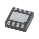
ICGOO电子元器件商城为您提供ADL5350ACPZ-R7由Analog设计生产,在icgoo商城现货销售,并且可以通过原厂、代理商等渠道进行代购。 ADL5350ACPZ-R7价格参考。AnalogADL5350ACPZ-R7封装/规格:RF 混频器, RF Mixer IC Cellular, CDMA, GSM 750MHz ~ 4GHz 8-LFCSP-VD (3x2)。您可以下载ADL5350ACPZ-R7参考资料、Datasheet数据手册功能说明书,资料中有ADL5350ACPZ-R7 详细功能的应用电路图电压和使用方法及教程。
ADL5350ACPZ-R7是Analog Devices Inc.推出的一款高性能有源混频器,属于RF混频器类别。该器件广泛应用于无线通信系统中,特别适用于需要高线性度、低噪声和优良动态范围的场景。

其典型应用场景包括:蜂窝通信基础设施中的宏基站、微波点对点通信、无线回传系统、宽带无线接入(如WLL)以及工业和军事通信设备。由于ADL5350ACPZ-R7具备宽频带工作能力(射频频率可达100MHz至2.5GHz,本振频率匹配范围广),非常适合多频段、多模式的射频接收前端设计。

该混频器采用有源结构,提供良好的端口隔离和较高的转换增益,有助于简化射频链路设计并减少外部放大需求。同时,它支持单端输入,降低了系统设计复杂度,适合集成在紧凑型高频电路中。此外,其出色的三阶交调性能(IIP3)和低噪声系数使其在强干扰环境下仍能保持良好的信号解调能力,适用于高密度信号环境下的接收机应用。

ADL5350ACPZ-R7常用于下变频环节,将接收到的高频RF信号转换为较低频率的中频(IF)信号,便于后续ADC采样与基带处理。其小型化的3mm × 3mm LFCSP封装,适合高密度PCB布局,广泛应用于便携式和固定式射频设备中。
| 参数 | 数值 |
| 产品目录 | |
| 描述 | IC MIXER 750MHZ-4GHZ 8LFCSP |
| 产品分类 | |
| 品牌 | Analog Devices Inc |
| 数据手册 | |
| 产品图片 |
|
| 产品型号 | ADL5350ACPZ-R7 |
| RF类型 | 手机,CDMA,GSM |
| rohs | 无铅 / 符合限制有害物质指令(RoHS)规范要求 |
| 产品系列 | ADL5350 |
| 产品目录页面 | |
| 供应商器件封装 | 8-LFCSP-VD(3x2) |
| 其它名称 | ADL5350ACPZ-R7CT |
| 包装 | 剪切带 (CT) |
| 噪声系数 | 6.5dB |
| 增益 | - |
| 封装/外壳 | 8-VFDFN 裸露焊盘,CSP |
| 标准包装 | 1 |
| 混频器数 | 1 |
| 电压-电源 | 2.7 V ~ 3.5 V |
| 电流-电源 | 16.5mA |
| 视频文件 | http://www.digikey.cn/classic/video.aspx?PlayerID=1364138032001&width=640&height=505&videoID=2245193150001 |
| 辅助属性 | - |
| 频率 | 750MHz ~ 4GHz |


- 商务部:美国ITC正式对集成电路等产品启动337调查
- 曝三星4nm工艺存在良率问题 高通将骁龙8 Gen1或转产台积电
- 太阳诱电将投资9.5亿元在常州建新厂生产MLCC 预计2023年完工
- 英特尔发布欧洲新工厂建设计划 深化IDM 2.0 战略
- 台积电先进制程称霸业界 有大客户加持明年业绩稳了
- 达到5530亿美元!SIA预计今年全球半导体销售额将创下新高
- 英特尔拟将自动驾驶子公司Mobileye上市 估值或超500亿美元
- 三星加码芯片和SET,合并消费电子和移动部门,撤换高东真等 CEO
- 三星电子宣布重大人事变动 还合并消费电子和移动部门
- 海关总署:前11个月进口集成电路产品价值2.52万亿元 增长14.8%


PDF Datasheet 数据手册内容提取
LF to 4 GHz, High Linearity Y-Mixer Data Sheet ADL5350 FEATURES FUNCTIONAL BLOCK DIAGRAM Broadband radio frequency (RF), intermediate frequency (IF), GND and local oscillator (LO) ports RF IF INPUT OR ADL5350 OUTPUT OR Conversion loss: 6.8 dB OUTPUT INPUT Noise figure: 6.5 dB RF IF High input IP3: 25 dBm High input P1dB: 19 dBm Low LO drive level 3V VPOS GND Single-ended design: no need for baluns Single-supply operation: 3 V at 19 mA Miniature, 2 mm × 3 mm, 8-lead LFCSP LO RAoPHPSL cIoCmApTlIiaOnNt S INLPOUT 05615-001 Figure 1. Cellular base stations Point-to-point radio links RF instrumentation GENERAL DESCRIPTION The ADL5350 is a high linearity, up-and-down converting The high input linearity of the ADL5350 makes the device an mixer capable of operating over a broad input frequency range. excellent mixer for communications systems that require high It is well suited for demanding cellular base station mixer designs blocker immunity, such as GSM 850 MHz/900 MHz and that require high sensitivity and effective blocker immunity. Based 800 MHz CDMA2000. At 2 GHz, a slightly greater supply on a GaAs pHEMT, single-ended mixer architecture, the ADL5350 current is required to obtain similar performance. provides excellent input linearity and a low noise figure without The single-ended broadband RF/IF port allows the device to be the need for a high power level LO drive. customized for a desired band of operation using simple external In 850 MHz/900 MHz receive applications, the ADL5350 filter networks. The LO-to-RF isolation is based on the LO provides a typical conversion loss of only 6.7 dB. The input IP3 rejection of the RF port filter network. Greater isolation can be is typically greater than 25 dBm, with an input compression achieved by using higher order filter networks, as described in point of 19 dBm. The integrated LO amplifier allows a low LO the Applications Information section. drive level, typically only 4 dBm for most applications. The ADL5350 is fabricated on a GaAs pHEMT, high performance IC process. The ADL5350 is available in a 2 mm × 3 mm, 8-lead LFCSP. It operates over a −40°C to +85°C temperature range. An evaluation board is also available. Rev. A Document Feedback Information furnished by Analog Devices is believed to be accurate and reliable. However, no responsibility is assumed by Analog Devices for its use, nor for any infringements of patents or other One Technology Way, P.O. Box 9106, Norwood, MA 02062-9106, U.S.A. rights of third parties that may result from its use. Specifications subject to change without notice. No license is granted by implication or otherwise under any patent or patent rights of Analog Devices. Tel: 781.329.4700 ©2008–2016 Analog Devices, Inc. All rights reserved. Trademarks and registered trademarks are the property of their respective owners. Technical Support www.analog.com
ADL5350 Data Sheet TABLE OF CONTENTS Features .............................................................................................. 1 Typical Performance Characteristics ..............................................7 Applications ....................................................................................... 1 850 MHz Characteristics ..............................................................7 Functional Block Diagram .............................................................. 1 1950 MHz Characteristics ......................................................... 12 General Description ......................................................................... 1 Functional Description .................................................................. 17 Revision History ............................................................................... 2 Circuit Description .................................................................... 17 Specifications ..................................................................................... 3 Implementation Procedure ....................................................... 17 850 MHz Receive Performance .................................................. 3 Applications Information .............................................................. 19 1950 MHz Receive Performance ................................................ 3 Low Frequency Applications .................................................... 19 Spur Tables ......................................................................................... 4 High Frequency Applications ................................................... 19 850 MHz Spur Table ..................................................................... 4 Evaluation Board ............................................................................ 21 1950 MHz Spur Table................................................................... 4 Outline Dimensions ....................................................................... 22 Absolute Maximum Ratings ............................................................ 5 Ordering Guide .......................................................................... 22 ESD Caution .................................................................................. 5 Pin Configuration and Function Descriptions ............................. 6 REVISION HISTORY 6/2016—Rev. 0 to Rev. A Changed CP-8-1 to CP-8-23 ........................................ Throughout Change to θ Parameter, Table 5 .................................................... 5 JA Changes to Figure 2 and Table 6 ..................................................... 6 Updated Outline Dimensions ....................................................... 22 Changes to Ordering Guide .......................................................... 22 2/2008—Revision 0: Initial Version Rev. A | Page 2 of 24
Data Sheet ADL5350 SPECIFICATIONS 850 MHz RECEIVE PERFORMANCE V = 3 V, T = 25°C, LO power = 4 dBm, re: 50 Ω, unless otherwise noted. S A Table 1. Parameter Min Typ Max Unit Test Conditions/Comments RF Frequency Range 750 850 975 MHz LO Frequency Range 500 780 945 MHz Low-side LO IF Frequency Range 30 70 250 MHz Conversion Loss 6.7 dB f = 850 MHz, f = 780 MHz, f = 70 MHz RF LO IF SSB Noise Figure 6.4 dB f = 850 MHz, f = 780 MHz, f = 70 MHz RF LO IF Input Third-Order Intercept (IP3) 25 dBm f = 849 MHz, f = 850 MHz, f = 780 MHz, f = 70 MHz; RF1 RF2 LO IF each RF tone 0 dBm Input 1dB Compression Point (P1dB) 19.8 dBm f = 820 MHz, f = 750 MHz, f = 70 MHz RF LO IF LO-to-IF Leakage 29 dBc LO power = 4 dBm, f = 780 MHz LO LO-to-RF Leakage 13 dBc LO power = 4 dBm, f = 780 MHz LO RF-to-IF Leakage 19.5 dBc RF power = 0 dBm, f = 850 MHz, f = 780 MHz RF LO IF/2 Spurious −50 dBc RF power = 0 dBm, f = 850 MHz, f = 780 MHz RF LO Supply Voltage 2.7 3 3.5 V Supply Current 16.5 mA LO power = 4 dBm 1950 MHz RECEIVE PERFORMANCE V = 3 V, T = 25°C, LO power = 6 dBm, re: 50 Ω, unless otherwise noted. S A Table 2. Parameter Min Typ Max Unit Test Conditions/Comments RF Frequency Range 1800 1950 2050 MHz LO Frequency Range 1420 1760 2000 MHz Low-side LO IF Frequency Range 50 190 380 MHz Conversion Loss 6.8 dB f = 1950 MHz, f = 1760 MHz, f = 190 MHz RF LO IF SSB Noise Figure 6.5 dB f = 1950 MHz, f = 1760 MHz, f = 190 MHz RF LO IF Input Third-Order Intercept (IP3) 25 dBm f = 1949 MHz, f = 1951 MHz, f = 1760 MHz, f = 190 MHz; RF1 RF2 LO IF each RF tone 0 dBm Input 1dB Compression Point (P1dB) 19 dBm f = 1950 MHz, f = 1760 MHz, f = 190 MHz RF LO IF LO-to-IF Leakage 13.5 dBc LO power = 6 dBm, f = 1760 MHz LO LO-to-RF Leakage 10.5 dBc LO power = 6 dBm, f = 1760 MHz LO RF-to-IF Leakage 11.5 dBc RF power = 0 dBm, f = 1950 MHz, f = 1760 MHz RF LO IF/2 Spurious −54 dBc RF power = 0 dBm, f = 1950 MHz, f = 1760 MHz RF LO Supply Voltage 2.7 3 3.5 V Supply Current 19 mA LO power = 6 dBm Rev. A | Page 3 of 24
ADL5350 Data Sheet SPUR TABLES All spur tables are (N × f ) − (M × f ) mixer spurious products for 0 dBm input power, unless otherwise noted. N.M. indicates that a RF LO spur was not measured due to it being at a frequency >6 GHz. 850 MHz SPUR TABLE Table 3. M 0 1 2 3 4 5 6 7 8 9 10 11 12 13 14 15 0 ≤–100 –20.6 –19.2 –15.3 –16.7 –38.4 –26.6 –22.1 N.M. N.M. N.M. N.M. N.M. N.M. N.M. N.M. 1 –21.6 –5.6 –23.6 –19.6 –31.9 –28.7 –46.1 –48.5 –33.2 N.M. N.M. N.M. N.M. N.M. N.M. N.M. 2 –50.0 –69.2 –50.5 –59.8 –49.1 –57.5 –51.0 –77.7 –65.8 –60.8 N.M. N.M. N.M. N.M. N.M. N.M. 3 –74.8 –66.0 –71.8 –68.1 –70.2 –67.4 –66.9 –70.8 –85.2 –87.3 –72.2 N.M. N.M. N.M. N.M. N.M. 4 ≤–100 –92.6 –91.6 –96.1 –92.7 –98.7 –90.2 –91.7 –88.8 ≤–100 ≤–100 –91.7 –88.6 N.M. N.M. N.M. 5 ≤–100 ≤–100 ≤–100 ≤–100 ≤–100 ≤–100 ≤–100 ≤–100 –99.5 ≤–100 ≤–100 ≤–100 ≤–100 ≤–100 N.M. N.M. 6 ≤–100 ≤–100 ≤–100 ≤–100 ≤–100 ≤–100 ≤–100 ≤–100 ≤–100 ≤–100 ≤–100 ≤–100 ≤–100 ≤–100 ≤–100 N.M. N 7 ≤–100 ≤–100 ≤–100 ≤–100 ≤–100 ≤–100 ≤–100 ≤–100 ≤–100 ≤–100 ≤–100 ≤–100 ≤–100 ≤–100 ≤–100 ≤–100 8 N.M. N.M. ≤–100 ≤–100 ≤–100 ≤–100 ≤–100 ≤–100 ≤–100 ≤–100 ≤–100 ≤–100 ≤–100 ≤–100 ≤–100 ≤–100 9 N.M. N.M. N.M. ≤–100 ≤–100 ≤–100 ≤–100 ≤–100 ≤–100 ≤–100 ≤–100 ≤–100 ≤–100 ≤–100 ≤–100 ≤–100 10 N.M. N.M. N.M. N.M. ≤–100 ≤–100 ≤–100 ≤–100 ≤–100 ≤–100 ≤–100 ≤–100 ≤–100 ≤–100 ≤–100 ≤–100 11 N.M. N.M. N.M. N.M. N.M. ≤–100 ≤–100 ≤–100 ≤–100 ≤–100 ≤–100 ≤–100 ≤–100 ≤–100 ≤–100 ≤–100 12 N.M. N.M. N.M. N.M. N.M. N.M. ≤–100 ≤–100 ≤–100 ≤–100 ≤–100 ≤–100 ≤–100 ≤–100 ≤–100 ≤–100 13 N.M. N.M. N.M. N.M. N.M. N.M. N.M. ≤–100 ≤–100 ≤–100 ≤–100 ≤–100 ≤–100 ≤–100 ≤–100 ≤–100 1154 NN..MM.. NN..MM.. NN..MM.. NN..MM.. NN..MM.. NN..MM.. NN..MM.. NN..MM.. N≤–.M10.0 ≤≤––110000 ≤≤––110000 ≤≤––110000 ≤≤––110000 ≤≤––110000 ≤≤––110000 ≤≤––110000 05615–068 1950 MHz SPUR TABLE Table 4. M 0 1 2 3 4 5 6 7 8 9 10 11 12 13 14 15 0 ≤–100 –13.1 –32.8 –22.4 N.M. N.M. N.M. N.M. N.M. N.M. N.M. N.M. N.M. N.M. N.M. N.M. 1 –10.8 –7.0 –25.3 –27.7 –33.9 N.M. N.M. N.M. N.M. N.M. N.M. N.M. N.M. N.M. N.M. N.M. 2 –48.2 –61.2 –41.2 –44.6 –47.0 –74.6 N.M. N.M. N.M. N.M. N.M. N.M. N.M. N.M. N.M. N.M. 3 –72.3 –71.4 –83.6 –64.5 –62.4 –64.3 –83.7 N.M. N.M. N.M. N.M. N.M. N.M. N.M. N.M. N.M. 4 N.M. N.M. –91.4 –84.2 –78.3 –76.5 –80.0 –92.0 N.M. N.M. N.M. N.M. N.M. N.M. N.M. N.M. 5 N.M. N.M. N.M. –90.8 –82.3 –77.1 –79.5 –83.8 –95.2 N.M. N.M. N.M. N.M. N.M. N.M. N.M. 6 N.M. N.M. N.M. N.M.≤ –100 ≤–100 –93.4 –94.5 ≤–100 –99.2 ≤–100 N.M. N.M. N.M. N.M. N.M. N 7 N.M. N.M. N.M. N.M. N.M. ≤–100 ≤–100 –94.0 –96.4 ≤–100 ≤–100 ≤–100 N.M. N.M. N.M. N.M. 8 N.M. N.M. N.M. N.M. N.M. N.M.≤ –100 ≤–100 ≤–100 ≤–100 ≤–100 ≤–100 ≤–100 N.M. N.M. N.M. 9 N.M. N.M. N.M. N.M. N.M. N.M. N.M. ≤–100 ≤–100 ≤–100 ≤–100 ≤–100 ≤–100 ≤–100 N.M. N.M. 10 N.M. N.M. N.M. N.M. N.M. N.M. N.M. N.M. ≤–100 ≤–100 ≤–100 ≤–100 ≤–100 ≤–100 ≤–100 N.M. 11 N.M. N.M. N.M. N.M. N.M. N.M. N.M. N.M. N.M. ≤–100 ≤–100 ≤–100 ≤–100 ≤–100 ≤–100 ≤–100 12 N.M. N.M. N.M. N.M. N.M. N.M. N.M. N.M. N.M. N.M. ≤–100 ≤–100 ≤–100 ≤–100 ≤–100 ≤–100 111345 NNN...MMM... NNN...MMM... NNN...MMM... NNN...MMM... NNN...MMM... NNN...MMM... NNN...MMM... NNN...MMM... NNN...MMM... NNN...MMM... NNN...MMM... ≤NN–..MM10..0 ≤NN–..MM10..0 ≤≤N––.M1100.00 ≤≤≤–––111000000 ≤≤≤–––111000000 05615–069 Rev. A | Page 4 of 24
Data Sheet ADL5350 ABSOLUTE MAXIMUM RATINGS Stresses at or above those listed under Absolute Maximum Table 5. Ratings may cause permanent damage to the product. This is a Parameter Rating stress rating only; functional operation of the product at these Supply Voltage, VS 4.0 V or any other conditions above those indicated in the operational RF Input Level 23 dBm section of this specification is not implied. Operation beyond LO Input Level 20 dBm the maximum operating conditions for extended periods may Internal Power Dissipation 324 mW affect product reliability. θ 33.2°C/W JA Maximum Junction Temperature 135°C Operating Temperature Range −40°C to +85°C ESD CAUTION Storage Temperature Range −65°C to +150°C Rev. A | Page 5 of 24
ADL5350 Data Sheet PIN CONFIGURATION AND FUNCTION DESCRIPTIONS RF/IF 1 8 RF/IF GND2 2 ADL5350 7 NIC TOP VIEW LOIN 3 (Not to Scale) 6 VPOS NIC 4 5 GND1 NOTES 12..NTTHOICE G= ER NXOOPUO INNSDTE.EDR PNAADL MCUOSNTN EBCET SIOONLD.ERED 05615-002 Figure 2. Pin Configuration Table 6. Pin Function Descriptions Pin No. Mnemonic Description 1, 8 RF/IF RF and IF Input/Output Ports. These nodes are internally tied together. RF and IF port separation is achieved using external tuning networks. 2, 5 GND2, GND1 Device Commons (DC Grounds). 3 LOIN LO Input. Needs to be ac-coupled. 4, 7 NIC No Internal Connection. Grounding NIC pins is recommended. 6 VPOS Positive Supply Voltage for the Drain of the LO Buffer. A series RF choke is needed on the supply line to provide proper ac loading of the LO buffer amplifier. 0 EPAD Exposed Pad. The exposed pad must be soldered to ground. Rev. A | Page 6 of 24
Data Sheet ADL5350 TYPICAL PERFORMANCE CHARACTERISTICS 850 MHz CHARACTERISTICS Supply voltage = 3 V, RF frequency = 850 MHz, IF frequency = 70 MHz, RF level = 0 dBm, LO level = 4 dBm, T = 25°C, unless otherwise noted. A 20 23 19 22 18 21 NT (mA) 1167 dBm) 2109 RE B ( UPPLY CUR 111345 INPUT P1d 111876 S 12 15 11 14 10–40 –20 0TEMPER2A0TURE (°4C0) 60 80 05615-003 13–40 –20 0TEMPER2A0TURE (°4C0) 60 80 05615-006 Figure 3. Supply Current vs. Temperature Figure 6. Input P1dB vs. Temperature 10 22 9 20 8 ON LOSS (dB) 765 URRENT (mA) 1186 +25°C SI C NVER 4 PPLY 14 –40°C +85°C O 3 U C S 2 12 1 0–40 –20 0TEMPER2A0TURE (°4C0) 60 80 05615-004 102.7 2.8 2.9 SU3P.0PLY V3O.1LTAG3E.2 (V) 3.3 3.4 3.5 05615-007 Figure 4. Conversion Loss vs. Temperature Figure 7. Supply Current vs. Supply Voltage 28 7.4 27 7.2 26 25 dB) 7.0 m) S ( +85°C INPUT IP3 (dB 222432 NVERSION LOS 66..86 +–4205°°CC 21 O 6.4 C 20 6.2 19 18–40 –20 0TEMPER2A0TURE (°4C0) 60 80 05615-005 6.02.7 2.8 2.9 SU3P.0PLY V3O.1LTAG3E.2 (V) 3.3 3.4 3.5 05615-008 Figure 5. Input IP3 vs. Temperature Figure 8. Conversion Loss vs. Supply Voltage Rev. A | Page 7 of 24
ADL5350 Data Sheet Supply voltage = 3 V, RF frequency = 850 MHz, IF frequency = 70 MHz, RF level = 0 dBm, LO level = 4 dBm, T = 25°C, unless otherwise noted. A 28 22 27 20 –40°C A) Bm) 26 +85°C NT (m 18 T IP3 (d 25 +25°C CURRE 16 –40°C INPU 24 PPLY 14 U S +85°C +25°C 23 12 222.7 2.8 2.9 SU3P.0PLY V3O.1LTAG3E.2 (V) 3.3 3.4 3.5 05615-009 10750 775 800 8R25F FR8E5Q0UEN8C7Y5 (MH9z0)0 925 950 975 05615-012 Figure 9. Input IP3 vs. Supply Voltage Figure 12. Supply Current vs. RF Frequency 23 7.6 7.4 22 7.2 21 B) +85°C Bm) –40°C SS (d 7.0 1dB (d 20 +25°C ON LO 6.8 +25°C INPUT P 1198 +85°C ONVERSI 66..64 –40°C C 6.2 17 6.0 162.7 2.8 2.9 SU3P.0PLY V3O.1LTAG3E.2 (V) 3.3 3.4 3.5 05615-010 5.8750 800 RF FREQU8E50NCY (MHz) 900 950 05615-013 Figure 10. Input P1dB vs. Supply Voltage Figure 13. Conversion Loss vs. RF Frequency 8.0 27.0 26.5 7.5 26.0 –40°C +25°C +85°C dB) 7.0 m) 25.5 GURE ( 6.5 P3 (dB 2245..50 SE FI PUT I 24.0 NOI 6.0 IN 23.5 23.0 5.5 22.5 5.02.7 2.8 2.9 SU3P.0PLY V3O.1LTAG3E. 2(V) 3.3 3.4 3.5 05615-011 22.0750 775 800 8R25F FR8E5Q0UEN8C7Y5 (MH9z0)0 925 950 975 05615-014 Figure 11. Noise Figure vs. Supply Voltage Figure 14. Input IP3 vs. RF Frequency Rev. A | Page 8 of 24
Data Sheet ADL5350 Supply voltage = 3 V, RF frequency = 850 MHz, IF frequency = 70 MHz, RF level = 0 dBm, LO level = 4 dBm, T = 25°C, unless otherwise noted. A 23 9 +85°C 8 22 +25°C 7 21 B) Bm) –40°C SS (d 6 dB (d 20 N LO 5 –40°C INPUT P1 1189 ++8255°°CC ONVERSIO 34 C 2 17 1 16750 775 800 8R25F FR8E5Q0UEN8C7Y5 (MH9z0)0 925 950 975 05615-015 025 50 75 10IF0 FRE1Q25UEN1C5Y0 (MH1z7)5 200 225 250 05615-018 Figure 15. Input P1dB vs. RF Frequency Figure 18. Conversion Loss vs. IF Frequency 8 28 7 27 6 –40°C GURE (dB) 54 P3 (dBm) 2256 +25°C NOISE FI 3 INPUT I 24 +85°C 2 23 1 0750 775 800 8R25F FR8E5Q0UEN8C7Y5 (MH9z0)0 925 950 975 05615-016 2225 50 75 10IF0 FRE1Q25UEN1C5Y0 (MH1z7)5 200 225 250 05615-019 Figure 16. Noise Figure vs. RF Frequency Figure 19. Input IP3 vs. IF Frequency 22 23 +25°C 20 22 A) 18 21 RENT (m 16 +85°C –40°C B (dBm) 20 –40°C SUPPLY CUR 1124 INPUT P1d 1198 +25°C +85°C 10 17 825 50 75 10IF0 FRE1Q25UEN1C5Y0 (MH1z7)5 200 225 250 05615-017 1625 50 75 10IF0 FRE1Q25UEN1C5Y0 (MH1z7)5 200 225 250 05615-020 Figure 17. Supply Current vs. IF Frequency Figure 20. Input P1dB vs. IF Frequency Rev. A | Page 9 of 24
ADL5350 Data Sheet Supply voltage = 3 V, RF frequency = 850 MHz, IF frequency = 70 MHz, RF level = 0 dBm, LO level = 4 dBm, T = 25°C, unless otherwise noted. A 10 27 –40°C 9 25 8 +25°C +85°C dB) 7 m) 23 GURE ( 56 P3 (dB 21 SE FI 4 PUT I 19 NOI 3 IN 17 2 15 1 050 100 150IF FRE2Q0U0ENCY 2(5M0Hz) 300 350 05615-021 13–6 –4 –2 0 LO L2EVEL (4dBm) 6 8 10 12 05615-024 Figure 21. Noise Figure vs. IF Frequency Figure 24. Input IP3 vs. LO Level 18 22 16 –40°C 21 14 A) 20 T (m 12 Bm) +25°C REN 10 B (d 19 SUPPLY CUR 86 +85°C –40°C INPUT P1d 1187 +85°C 4 +25°C 16 2 0–6 –4 –2 0 LO L2EVEL (4dBm) 6 8 10 12 05615-022 15–6 –4 –2 0 LO L2EVEL (4dBm) 6 8 10 12 05615-025 Figure 22. Supply Current vs. LO Level Figure 25. Input P1dB vs. LO Level 20 12 18 11 –40°C B) 16 10 RSION LOSS (d 1142 +25°C E FIGURE (dB) 98 VE OIS 7 N N O 10 C 6 +85°C 8 5 6–6 –4 –2 0 LO L2EVEL (4dBm) 6 8 10 12 05615-023 4–2 0 2 LO LEVE4L (dBm) 6 8 10 05615-026 Figure 23. Conversion Loss vs. LO Level Figure 26. Noise Figure vs. LO Level Rev. A | Page 10 of 24
Data Sheet ADL5350 Supply voltage = 3 V, RF frequency = 850 MHz, IF frequency = 70 MHz, RF level = 0 dBm, LO level = 4 dBm, T = 25°C, unless otherwise noted. A –13 0 –2 –14 –4 EEDTHROUGH (dBc) ––––11115678 –40°C F LEAKAGE (dBc) ––11––0268 F F +25°C R –14 I –19 –16 –20 –18 +85°C –21750 775 800 8R25F FR8E5Q0UEN8C7Y5 (MH9z0)0 925 950 975 05615-027 –20630 680 7L3O0 FREQU78E0NCY (MH8z3)0 880 930 05615-029 Figure 27. IF Feedthrough vs. RF Frequency Figure 29. RF Leakage vs. LO Frequency –15 +25°C –20 c) B d –25 H ( G +85°C U RO –30 H T D E FE –35 F I –40°C –40 –45680 705 730 7L5O5 FR7E8Q0UEN8C0Y5 (MH8z3)0 855 880 905 05615-028 Figure 28. IF Feedthrough vs. LO Frequency Rev. A | Page 11 of 24
ADL5350 Data Sheet 1950 MHz CHARACTERISTICS Supply voltage = 3 V, RF frequency = 1950 MHz, IF frequency = 190 MHz, RF level = −10 dBm, LO level = 6 dBm, T = 25°C, A unless otherwise noted. 20 23 19 22 18 21 NT (mA) 1176 dBm) 1290 RE B ( UPPLY CUR 111543 INPUT P1d 111678 S 12 15 11 14 10–40 –20 0TEMPER2A0TURE (°4C0) 60 80 05615-030 13–40 –20 0TEMPER2A0TURE (°4C0) 60 80 05615-033 Figure 30. Supply Current vs. Temperature Figure 33. Input P1dB vs. Temperature 10 22 9 +25°C 20 8 ON LOSS (dB) 567 URRENT (mA) 1186 –40°C +85°C SI C ER 4 LY NV PP 14 O 3 U C S 2 12 1 0–40 –20 0TEMPER2A0TURE (°4C0) 60 80 05615-031 102.7 2.8 2.9 SU3P.0PLY V3O.1LTAG3E.2 (V) 3.3 3.4 3.5 05615-034 Figure 31. Conversion Loss vs. Temperature Figure 34. Supply Current vs. Supply Voltage 28 7.4 27 7.2 26 +85°C 25 dB) 7.0 PUT IP3 (dBm) 222234 ERSION LOSS ( 66..68 +–4205°°CC N V I N 21 O 6.4 C 20 6.2 19 18–40 –20 0TEMPER2A0TURE (°4C0) 60 80 05615-032 6.02.7 2.8 2.9 SU3P.0PLY V3O.1LTAG3E.2 (V) 3.3 3.4 3.5 05615-035 Figure 32. Input IP3 vs. Temperature Figure 35. Conversion Loss vs. Supply Voltage Rev. A | Page 12 of 24
Data Sheet ADL5350 Supply voltage = 3 V, RF frequency = 1950 MHz, IF frequency = 190 MHz, RF level = −10 dBm, LO level = 6 dBm, T = 25°C, A unless otherwise noted. 28 22 +25°C 27 20 Bm) 26 +85°C NT (mA) 18 +85°C –40°C INPUT IP3 (d 2245 +–4205°°CC PPLY CURRE 1164 U S 23 12 222.7 2.8 2.9 SU3P.0PLY V3O.1LTAG3E.2 (V) 3.3 3.4 3.5 05615-036 110800 1825 1850 1875RF1 F9R00EQ1U9E2N5CY19 (5M0Hz1)975 2000 2025 2050 05615-039 Figure 36. Input IP3 vs. Supply Voltage Figure 39. Supply Current vs. RF Frequency 20 7.6 +25°C 7.4 7.2 19 B) +85°C INPUT P1dB (dBm) 18 +85°C –40°C ONVERSION LOSS (d 6667....4680 +–4205°°CC 17 C 6.2 6.0 162.7 2.8 2.9 SU3P.0PLY V3O.1LTAG3E.2 (V) 3.3 3.4 3.5 05615-037 5.18800 1825 1850 1875RF1 F9R00EQ1U9E2N5CY19 (5M0Hz1)975 2000 2025 2050 05615-040 Figure 37. Input P1dB vs. Supply Voltage Figure 40. Conversion Loss vs. RF Frequency 8.0 27.0 26.5 7.5 26.0 +85°C B) 7.0 25.5 RE (d dBm) 25.0 +25°C NOISE FIGU 66..50 INPUT IP3 ( 2244..05 –40°C 23.5 23.0 5.5 22.5 5.02.7 2.8 2.9 SU3P.0PLY V3O.1LTAG3E.2 (V) 3.3 3.4 3.5 05615-038 22.10800 1825 1850 1875RF1 F9R00EQ1U9E2N5CY19 (5M0Hz1)975 2000 2025 2050 05615-041 Figure 38. Noise Figure vs. Supply Voltage Figure 41. Input IP3 vs. RF Frequency Rev. A | Page 13 of 24
ADL5350 Data Sheet Supply voltage = 3 V, RF frequency = 1950 MHz, IF frequency = 190 MHz, RF level = −10 dBm, LO level = 6 dBm, T = 25°C, A unless otherwise noted. 23 9 8 22 +85°C 7 21 dB) m) S ( 6 B –40°C S +25°C –40°C dB (d 20 +25°C N LO 5 1 O T P 19 RSI 4 NPU NVE 3 I 18 CO +85°C 2 17 1 116800 1825 1850 1875RF1 F9R00EQ1U9E2N5CY19 (5M0Hz1)975 2000 2025 2050 05615-042 050 75 100 125 150IF1 F7R5E2Q0U0EN22C5Y 2(M50Hz2)75 300 325 350 375 05615-045 Figure 42. Input P1dB vs. RF Frequency Figure 45. Conversion Loss vs. IF Frequency 10 28 9 27 8 +85°C dB) 7 m) 26 +25°C GURE ( 6 P3 (dB 25 E FI 5 UT I NOIS 4 INP 24 –40°C 3 23 2 11800 1825 1850 1875RF1 F9R00EQ1U9E2N5CY19 (5M0Hz1)975 2000 2025 2050 05615-043 2250 75 100 125 150IF1 F7R5E2Q0U0EN22C5Y 2(M50Hz2)75 300 325 350 375 05615-046 Figure 43. Noise Figure vs. RF Frequency Figure 46. Input IP3 vs. IF Frequency 22 23 +25°C 20 22 A) 18 21 T (m +85°C –40°C Bm) Y CURREN 1164 UT P1dB (d 1290 –40°C SUPPL 12 INP 18 +85°C +25°C 10 17 850 75 100 125 150IF1 F7R5E2Q0U0EN22C5Y (2M50Hz2)75 300 325 350 375 05615-044 1650 75 100 125 150IF1 F7R5E2Q0U0EN22C5Y 2(M50Hz2)75 300 325 350 375 05615-047 Figure 44. Supply Current vs. IF Frequency Figure 47. Input P1dB vs. IF Frequency Rev. A | Page 14 of 24
Data Sheet ADL5350 Supply voltage = 3 V, RF frequency = 1950 MHz, IF frequency = 190 MHz, RF level = −10 dBm, LO level = 6 dBm, T = 25°C, A unless otherwise noted. 12 27 +25°C 25 10 +85°C 23 dB) 8 m) –40°C GURE ( 6 P3 (dB 21 E FI UT I 19 S P NOI 4 IN 17 2 15 050 100 150IF FRE2Q0U0ENCY 2(5M0Hz) 300 350 05615-048 13–6 –4 –2 0 LO L2EVEL (4dBm) 6 8 10 12 05615-051 Figure 48. Noise Figure vs. IF Frequency Figure 51. Input IP3 vs. LO Level 22 25 20 24 +25°C –40°C 23 18 22 A) 16 RENT (m 1124 –40°C+85°C B (dBm) 221019 +25°C R d UPPLY CU 108 INPUT P1 111867 +85°C S 6 15 4 14 2 13 0–6 –4 –2 0 LO L2EVEL (4dBm) 6 8 10 12 05615-049 12–6 –4 –2 0 LO L2EVEL (4dBm) 6 8 10 12 05615-052 Figure 49. Supply Current vs. LO Level Figure 52. Input P1dB vs. LO Level 20 12 –40°C 18 11 +25°C RSION LOSS (dB) 111642 +85°C E FIGURE (dB) 1098 VE OIS 7 N N O 10 C 6 8 5 6–6 –4 –2 0 LO L2EVEL (4dBm) 6 8 10 12 05615-050 4–2 0 2 LO LEVE4L (dBm) 6 8 10 05615-053 Figure 50. Conversion Loss vs. LO Level Figure 53. Noise Figure vs. LO Level Rev. A | Page 15 of 24
ADL5350 Data Sheet Supply voltage = 3 V, RF frequency = 1950 MHz, IF frequency = 190 MHz, RF level = −10 dBm, LO level = 6 dBm, T = 25°C, A unless otherwise noted. –8 0 –9 –2 H (dBc) –10 dBc) –4 EEDTHROUG ––1112 –40°C F LEAKAGE ( ––86 F R F –13 –10 I +85°C +25°C –14 –12 –115800 1825 1850 1875RF1 F9R00EQ1U9E2N5CY19 (5M0Hz1)975 2000 2025 2050 05615-054 –114560 1610 1660 LO17 F10REQ1U7E6N0CY 1(M81H0z) 1860 1910 1960 05615-056 Figure 54. IF Feedthrough vs. RF Frequency Figure 56. RF Leakage vs. LO Frequency –8 –9 –10 Bc) –11 d GH ( –12 U RO –13 H T D –14 –40°C E E F F –15 I –16 +85°C +25°C –17 –118610 1635 1660 1685LO1 F7R10EQ1U7E3N5CY17 (6M0Hz1)785 1810 1835 1860 05615-055 Figure 55. IF Feedthrough vs. LO Frequency Rev. A | Page 16 of 24
Data Sheet ADL5350 FUNCTIONAL DESCRIPTION CIRCUIT DESCRIPTION IMPLEMENTATION PROCEDURE The ADL5350 is a GaAs pHEMT, single-ended, passive The ADL5350 is a simple single-ended mixer that relies mixer with an integrated LO buffer amplifier. The device on off-chip circuitry to achieve effective RF dynamic relies on the varying drain to source channel conductance performance. The following steps should be followed of a FET junction to modulate an RF signal. A simplified to achieve optimum performance (see Figure 58 for schematic is shown in Figure 57. component designations): VS INRPFUT VS OR OUTPUT IF C4 C6 L2 C2 L4 VPOS RF IF IOFUTPUT 8 7 6 5 LO LOIN OR INPUT RF/IF NIC VPOS GND1 INPUT ADL5350 RF/IF GND2 LOIN NIC FiguGrNe D517. SimplifiGeNdD S2chematic 05615-057 RF L1 C11 2 3 L3 4 bTuhfef eLrO am sipglnifaile irs. Taphpel ibeudf fteor tahme pglaitfeie cro pnrtoavcitd oefs as uFfEfiTc-iebnats ed LOC3 05615-058 gain of the LO signal to drive the resistive switch. Additionally, Figure 58. Reference Schematic feedback circuitry provides the necessary bias to the FET 1. Table 7 shows the recommended LO bias inductor buffer amplifier and RF/IF ports to achieve optimum values for a variety of LO frequencies. To ensure efficient modulation efficiency for common cellular frequencies. commutation of the mixer, the bias inductor needs to The mixing of RF and LO signals is achieved by switching be properly set. For other frequencies within the range the channel conductance from the RF/IF port to ground at shown, the values can be interpolated. For frequencies the rate of the LO. The RF signal is passed through an external outside this range, see the Applications Information band-pass network to help reject image bands and reduce section. the broadband noise presented to the mixer. The band- Table 7. Recommended LO Bias Inductor limited RF signal is presented to the time-varying load of Recommended LO Bias the RF/IF port, which causes the envelope of the RF signal Desired LO Frequency (MHz) Inductor, L41 (nH) to be amplitude modulated at the rate of the LO. A filter 380 68 network applied to the IF port is necessary to reject the 750 24 RF signal and pass the wanted mixing product. In a down- 1000 18 conversion application, the IF filter network is designed to 1750 3.8 pass the difference frequency and present an open circuit 2000 2.1 to the incident RF frequency. Similarly, for an upconversion 1 The bias inductor should have a self-resonant frequency greater than application, the filter is designed to pass the sum frequency the intended frequency of operation. and reject the incident RF. As a result, the frequency response of the mixer is determined by the response characteristics of the external RF/IF filter networks. Rev. A | Page 17 of 24
ADL5350 Data Sheet 2. Tune the LO port input network for optimum return If a better than −10 dB return loss is desired, it may be loss. Typically, a band-pass network is used to pass the necessary to add a shunt resistor to ground before the LO signal to the LOIN pin. It is recommended to block coupling capacitor (C3) to present a lower loading high frequency harmonics of the LO from the mixer impedance to the LO source. In doing so, a slightly core. LO harmonics cause higher RF frequency images greater LO drive level may be required. to be downconverted to the desired IF frequency and 3. Design the RF and IF filter networks. Figure 58 depicts result in sensitivity degradation. If the intended LO simple LC tank filter networks for the IF and RF port source has poor harmonic distortion and spectral interfaces. The RF port LC network is designed to pass purity, it may be necessary to employ a higher order the RF input signal. The series LC tank has a resonant band-pass filter network. Figure 58 illustrates a simple frequency at 1/(2π√LC). At resonance, the series LC band-pass filter used to pass the fundamental reactances are canceled, which presents a series short frequency of the LO source. Capacitor C3 is a simple to the RF signal. A parallel LC tank is used on the IF dc block, while the Series Inductor L3, along with the port to reject the RF and LO signals. At resonance, the gate-to-source capacitance of the buffer amplifier, parallel LC tank presents an open circuit. form a low-pass network. The native gate input of the It is necessary to account for the board parasitics, finite LO buffer (FET) alone presents a rather high input Q, and self-resonant frequencies of the LC components impedance. The gate bias is generated internally using when designing the RF, IF, and LO filter networks. Table 8 feedback that can result in a positive return loss at the provides suggested values for initial prototyping. intended LO frequency. Table 8. Suggested RF, IF, and LO Filter Networks for Low-Side LO Injection RF Frequency (MHz) L1 (nH)1 C1 (pF) L2 (nH) C2 (pF) L3 (nH) C3 (pF) 450 8.3 10 10 10 10 100 850 6.8 4.7 4.7 5.6 8.2 100 1950 1.7 1.5 1.7 1.2 3.5 100 2400 0.67 1 1.5 0.7 3.0 100 1 The inductor should have a self-resonant frequency greater than the intended frequency of operation. L1 should be a high Q inductor for optimum NF performance. Rev. A | Page 18 of 24
Data Sheet ADL5350 APPLICATIONS INFORMATION LOW FREQUENCY APPLICATIONS HIGH FREQUENCY APPLICATIONS The ADL5350 can be used in low frequency applications. The The ADL5350 can be used at extended frequencies with some circuit in Figure 59 is designed for an RF of 136 MHz to 176 MHz careful attention to board and component parasitics. Figure 61 and an IF of 45 MHz using a high-side LO. The series and is an example of a 2560 MHz to 2660 MHz downconversion parallel resonant circuits are tuned for 154 MHz, which is using a low-side LO. The performance of this circuit is depicted the geometric mean of the desired RF frequencies. The in Figure 62. Note that the inductor and capacitor values are performance of this circuit is depicted in Figure 60. very small, especially for the RF and IF ports. Above 2.5 GHz, 3V it is necessary to consider alternate solutions to avoid unreasonably small inductor and capacitor values. 4.7µF 3V 100nF IF 4.7µF 10nF + 36nH 27pF 100nH IF 1nF 100pF 8 7 6 5 1.5nH 0.7pF 2.1nH ALL INDUCTORS RF/IF NIC VPOS GND1 ARE 0603CS SERIES FROM ADL5350 8 7 6 5 COILCRAFT ALL INDUCTORS RF/IF NIC VPOS GND1 RF/IF GND2 LOIN NIC ARE 0302CS 1 2 3 4 SERIES FROM ADL5350 COILCRAFT 36nH RF/IF GND2 LOIN NIC RF 1nF 1 2 3 4 27pF LO 05615-061 RF 0.67nH1pF 3.0nH Figure 59. 136 MHz to 176 MHz RF Downconversion Schematic 100pF 40 12 LO 05615-062 Figure 61. 2560 MHz to 2660 MHz RF Downconversion Schematic IIP3 35 10 35 14 B) d m) 30 8 S ( 30 13 dB OS IIP3 IP1dB, IIP3 ( 2250 LIPO1SdSB 64 ONVERSION L P3 (dBm) 2250 IP1dB 1121 N LOSS (dB) 15 2 C P1dB, II 15 10 VERSIO I N 10 9 O C 10136 146 RF FREQU15E6NCY (MHz) 166 1760 05615-065 5 LOSS 8 Figure 60. Measured Performance for Circuit in Figure 59 Using High-Side LO Injection and 45 MHz IF 20560 2580 RF2 F6R00EQUENCY26 (2M0Hz) 2640 26607 05615-066 Figure 62. Measured Performance for Circuit in Figure 61 Using Low-Side LO Injection and 374 MHz IF The typical networks used for cellular applications below 2.6 GHz use band-select and band-reject networks on the RF and IF ports. At higher RF frequencies, these networks are not easily realized by using lumped element components. As a result, it is necessary to consider alternate filter network topologies to allow more reasonable values for inductors and capacitors. Rev. A | Page 19 of 24
ADL5350 Data Sheet Figure 63 depicts a crossover filter network approach to provide Classic audio crossover filter design techniques can be applied isolation between the RF and IF ports for a downconverting to help derive component values. However, some caution must be application. The crossover network essentially provides a high- applied when selecting component values. At high RF frequencies, pass filter to allow the RF signal to pass to the RF/IF node (Pin 1 the board parasitics can significantly influence the final optimum and Pin 8), while presenting a low-pass filter (which is actually inductor and capacitor component selections. Some empirical a band-pass filter when considering the dc blocking capacitor, testing may be necessary to optimize the RF and IF port filter C ). This allows the difference component (f − f ) to be networks. The performance of the circuit depicted in Figure 63 AC RF LO passed to the desired IF load. is provided in Figure 64. 3V 30 14 4.7µF IF C2 C10A0CpF + 100pF 25 IIP3 12 1.8pF B) d L1.25nH 3.8nH dBm) 20 10 OSS ( AIASNELRDLREUI E0C3ST0 OF2RCRSSOM RF8/IF NA7ICDL53VP56O0S GN5D1 IP1dB, IIP3 ( 1150 IP1dB LOSS 68 NVERSION L COILCRAFT RF/IF GND2 LOIN NIC CO 1 2 3 4 5 4 RF 2.2nH C1 3.5nLH1 1.2pF LO100pF 05615-064 3030F0igure 643.4 M00easurRedF3 FP5Re00rEfQoUrmENaCnY3c6 e(0M f0oHrz C)ircu3it7 i0n0 Figure 63830 02 05615-067 Figure 63. 3.3 GHz to 3.8 GHz RF Downconversion Schematic Using Low-Side LO Injection and 800 MHz IF When designing the RF port and IF port networks, it is important to remember that the networks share a common node (the RF/IF pins). In addition, the opposing network presents some loading impedance to the target network being designed. Rev. A | Page 20 of 24
Data Sheet ADL5350 EVALUATION BOARD An evaluation board is available for the ADL5350. The evaluation board has two halves: a low band board designated as Board A and a high band board designated as Board B. The schematic for the evaluation board is shown in Figure 65. VPOS-A VPOS-B C5-A C5-B + + IF-A IF-B C6-A C4-A C6-B C4-B L2-A C2-A L2-B C2-B L4-A L4-B 8 7 6 5 8 7 6 5 RF/IF NIC VPOS GND1 RF/IF NIC VPOS GND1 U1-A U1-B ADL5350 ADL5350 RF/IF GND2 LOIN NIC RF/IF GND2 LOIN NIC 1 2 3 4 1 2 3 4 RF-A L3-A RF-B L3-B L1-A C1-A L1-B C1-B C3-A C3-B LO-A LO-B 05615-059 Figure 65. Evaluation Board Table 9. Evaluation Board Configuration Options Component Function Default Conditions C4-A, C4-B, Supply Decoupling. C4-A and C4-B provide local bypassing of the supply. C5-A and C4-A = C4-B = 100 pF, C5-A, C5-B C5-B are used to filter the ripple of a noisy supply line. These are not always necessary. C5-A = C5-B = 4.7 µF L1-A, L1-B, RF Input Network. Designed to provide series resonance at the intended RF frequency. L1-A = 6.8 nH (0603CS from Coilcraft), C1-A, C1-B L1-B = 1.7 nH (0302CS from Coilcraft), C1-A = 4.7 pF, C1-B = 1.5 pF L2-A, L2-B, IF Output Network. Designed to provide parallel resonance at the geometric mean L2-A = 4.7 nH (0603CS from Coilcraft), C2-A, C2-B, of the RF and LO frequencies. L2-B = 1.7 nH (0302CS from Coilcraft), C6-A, C6-B C2-A = 5.6 pF, C2-B = 1.2 pF, C6-A = C6-B = 1 nF L3-A, L3-B, LO Input Network. Designed to block dc and optimize LO voltage swing at LOIN. L3-A = 8.2 nH (0603CS from Coilcraft), C3-A, C3-B L3-B = 3.5 nH (0302CS from Coilcraft), C3-A = C3-B = 100 pF L4-A, L4-B LO Buffer Amplifier Choke. Provides bias and ac loading impedance to LO buffer L4-A = 24 nH (0603CS from Coilcraft), amplifier. L4-B = 3.8 nH (0302CS from Coilcraft) Rev. A | Page 21 of 24
ADL5350 Data Sheet OUTLINE DIMENSIONS 3.25 1.89 3.00 0.55 1.74 2.75 0.40 1.59 0.30 0.20 MIN 2.25 5 8 2.00 EXPOSED PAD 0.60 1.75 0.45 4 1 0.30 PIN 1 INDEX TOP VIEW BOTTOM VIEW PIN 1 AREA 0.50 BSC INDICATOR 0.80 FOR PROPER CONNECTION OF 0.75 0.05 MAX TTHHEE PEIXNP COOSNEDFI GPAUDR,A RTEIOFNE RA NTOD 0.70 0.02 NOM FUNCTION DESCRIPTIONS SECTION OF THIS DATA SHEET. 0.30 PKG-004467 SEPALTAINNGE 00..2138 0.203 REF 02-12-2014-A Figure 66. 8-Lead Lead Frame Chip Scale Package [LFCSP] 2 mm × 3 mm Body and 0.75 mm Package Height (CP-8-23) Dimensions shown in millimeters ORDERING GUIDE Package Ordering Model1 Temperature Range Package Description Option Branding Quantity ADL5350ACPZ-R2 −40°C to +85°C 8-Lead Lead Frame Chip Scale Package [LFCSP] CP-8-23 08 240, Reel ADL5350ACPZ-R7 −40°C to +85°C 8-Lead Lead Frame Chip Scale Package [LFCSP] CP-8-23 08 3000, Reel ADL5350ACPZ-WP −40°C to +85°C 8-Lead Lead Frame Chip Scale Package [LFCSP] CP-8-23 08 50, Waffle Pack ADL5350-EVALZ Evaluation Board 1 Z = RoHS Compliant Part. Rev. A | Page 22 of 24
Data Sheet ADL5350 NOTES Rev. A | Page 23 of 24
ADL5350 Data Sheet NOTES ©2008–2016 Analog Devices, Inc. All rights reserved. Trademarks and registered trademarks are the property of their respective owners. D05615-0-6/16(A) Rev. A | Page 24 of 24
Mouser Electronics Authorized Distributor Click to View Pricing, Inventory, Delivery & Lifecycle Information: A nalog Devices Inc.: ADL5350ACPZ-R7 ADL5350-EVALZ