ICGOO在线商城 > 射频/IF 和 RFID > RF 混频器 > AD831APZ
 Datasheet下载
- 型号: AD831APZ
- 制造商: Analog
- 库位|库存: xxxx|xxxx
- 要求:
| 数量阶梯 | 香港交货 | 国内含税 |
| +xxxx | $xxxx | ¥xxxx |
查看当月历史价格
查看今年历史价格
AD831APZ产品简介:
ICGOO电子元器件商城为您提供AD831APZ由Analog设计生产,在icgoo商城现货销售,并且可以通过原厂、代理商等渠道进行代购。 AD831APZ价格参考。AnalogAD831APZ封装/规格:RF 混频器, RF Mixer IC HF, VHF Down Converter 500MHz 20-PLCC (9x9)。您可以下载AD831APZ参考资料、Datasheet数据手册功能说明书,资料中有AD831APZ 详细功能的应用电路图电压和使用方法及教程。
AD831APZ 是 Analog Devices Inc. 生产的一款 RF 混频器,广泛应用于射频 (RF) 和微波通信系统中。其主要应用场景包括无线通信、雷达系统、测试与测量设备等。

在无线通信领域,AD831APZ 用于实现频率转换,将接收的高频信号下变频为中频信号,或把基带信号上变频为高频信号。这种频率转换是通信系统中的关键步骤,有助于提高信号处理效率和减少干扰。例如,在蜂窝基站、Wi-Fi 路由器和卫星通信设备中,AD831APZ 可以帮助实现更高效的信号传输和接收。

在雷达系统中,AD831APZ 用于信号处理环节,特别是在脉冲压缩、频率捷变和多普勒效应检测等方面。它能够快速准确地进行频率转换,确保雷达系统具备高分辨率和远距离探测能力。此外,AD831APZ 的低噪声特性和高线性度使其适合用于高性能雷达应用,如气象雷达、空中交通管制雷达等。

测试与测量设备也是 AD831APZ 的重要应用场景之一。在这些设备中,混频器用于生成和分析不同频率的信号,帮助工程师评估和优化射频电路性能。例如,在频谱分析仪、矢量网络分析仪和信号发生器中,AD831APZ 可以提供精确的频率转换功能,确保测量结果的准确性。

总之,AD831APZ 凭借其优异的性能和可靠性,成为众多射频和微波应用的理想选择。无论是通信系统、雷达还是测试设备,它都能有效提升系统的性能和稳定性。
| 参数 | 数值 |
| 产品目录 | |
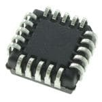
| 描述 | IC MIXER 500MHZ DWN CONV 20PLCC射频混合器 Hi-Perf Low Distort 500 MHz |
| DevelopmentKit | EVAL-AD831EBZ |
| 产品分类 | |
| 品牌 | Analog Devices |
| 产品手册 | |
| 产品图片 |
|
| rohs | 符合RoHS无铅 / 符合限制有害物质指令(RoHS)规范要求 |
| 产品系列 | RF集成电路,射频混合器,Analog Devices AD831APZAD831 |
| 数据手册 | |
| 产品型号 | AD831APZ |
| RF类型 | HF,VHF |
| 产品目录页面 | |
| 产品种类 | 射频混合器 |
| 供应商器件封装 | 20-PLCC(9x9) |
| 包装 | 管件 |
| 商标 | Analog Devices |
| 噪声系数 | 10.3 dB |
| 增益 | 0dB |
| 安装风格 | SMD/SMT |
| 封装 | Tube |
| 封装/外壳 | 20-LCC(J 形引线) |
| 封装/箱体 | PLCC-20 |
| 工作电源电压 | 4.5 V to 5.5 V |
| 工厂包装数量 | 49 |
| 最大功率耗散 | 1200 mW |
| 最大工作温度 | + 85 C |
| 最小工作温度 | - 40 C |
| 标准包装 | 49 |
| 混频器数 | 1 |
| 电压-电源 | 4.5 V ~ 5.5 V |
| 电流-电源 | 125mA |
| 电源电流 | 100 mA |
| 类型 | Mixers |
| 系列 | AD831 |
| 视频文件 | http://www.digikey.cn/classic/video.aspx?PlayerID=1364138032001&width=640&height=505&videoID=2245193150001 |
| 辅助属性 | 降频变频器 |
| 频率 | 500MHz |
| 频率范围 | 400 MHz |


- 商务部:美国ITC正式对集成电路等产品启动337调查
- 曝三星4nm工艺存在良率问题 高通将骁龙8 Gen1或转产台积电
- 太阳诱电将投资9.5亿元在常州建新厂生产MLCC 预计2023年完工
- 英特尔发布欧洲新工厂建设计划 深化IDM 2.0 战略
- 台积电先进制程称霸业界 有大客户加持明年业绩稳了
- 达到5530亿美元!SIA预计今年全球半导体销售额将创下新高
- 英特尔拟将自动驾驶子公司Mobileye上市 估值或超500亿美元
- 三星加码芯片和SET,合并消费电子和移动部门,撤换高东真等 CEO
- 三星电子宣布重大人事变动 还合并消费电子和移动部门
- 海关总署:前11个月进口集成电路产品价值2.52万亿元 增长14.8%


PDF Datasheet 数据手册内容提取
Low Distortion Mixer AD831 FEATURES FUNCTIONAL BLOCK DIAGRAM Doubly Balanced Mixer Low Distortion �� ��� �� ��� �� +24 dBm Third Order Intercept (IP3) � � � �� �� +10 dBm 1 dB Compression Point ��� ��� Low LO Drive Required: –10 dBm ��� � �� ��� Bandwidth �� � �� ��� 500 MHz RF and LO Input Bandwidths ��� � �� ��� 250 MHz Differential Current IF Output DC to >200 MHz Single-Ended Voltage IF Output ��� � �� �� ����� Single- or Dual-Supply Operation �� � �� ���� DC Coupled Using Dual Supplies All Ports May Be DC Coupled � �� �� �� �� � � � � � No Lower Frequency Limit—Operation to DC � � � � � � � � User-Programmable Power Consumption APPLICATIONS building a quadrature-amplitude modulator or image reject mixer, High Performance RF/IF Mixer the differential current outputs of two AD831s may be summed Direct to Baseband Conversion by connecting them together. Image-Reject Mixers I/Q Modulators and Demodulators An integral low noise amplifier provides a single-ended voltage output and can drive such low impedance loads as filters, 50 amplifier inputs, and A/D converters. Its small signal bandwidth exceeds 200 MHz. A single resistor connected between pins PRODUCT DESCRIPTION OUT and FB sets its gain. The amplifier’s low dc offset allows The AD831 is a low distortion, wide dynamic range, monolithic its use in such direct-coupled applications as direct-to-baseband mixer for use in such applications as RF to IF downconversion conversion and quadrature-amplitude demodulation. in HF and VHF receivers, the second mixer in DMR base sta- tions, direct-to-baseband conversion, quadrature modulation and The mixer’s SSB noise figure is 10.3 dB at 70 MHz using its demodulation, and doppler shift detection in ultrasound imaging output amplifier and optimum source impedance. Unlike passive applications. The mixer includes an LO driver and a low noise mixers, the AD831 has no insertion loss and does not require an output amplifier and provides both user-programmable power external diplexer or passive termination. consumption and third order intercept point. A programmable-bias feature allows the user to reduce power The AD831 provides a +24 dBm third order intercept point for consumption, with a reduction in the 1 dB compression point and –10 dBm LO power, thus improving system performance and third-order intercept. This permits a tradeoff between dynamic reducing system cost compared to passive mixers, by eliminating range and power consumption. For example, the AD831 may be the need for a high power LO driver and its attendant shielding used as a second mixer in cellular and two-way radio base stations and isolation problems. at reduced power while still providing a substantial performance improvement over passive solutions. The RF, IF, and LO ports may be dc or ac coupled when the mixer is operating from ±5 V supplies or ac coupled when oper- PRODUCT HIGHLIGHTS ating from a single-supply of 9 V minimum. The mixer operates 1. –10 dBm LO Drive for a +24 dBm Output Referred Third with RF and LO inputs as high as 500 MHz. Order Intercept Point The mixer’s IF output is available as either a differential current 2. Single-Ended Voltage Output output or a single-ended voltage output. The differential output is from a pair of open collectors and may be ac coupled via a trans- 3. High Port-to-Port Isolation former or capacitor to provide a 250 MHz output bandwidth. In 4. No Insertion Loss downconversion applications, a single capacitor connected across 5. Single- or Dual-Supply Operation these outputs implements a low-pass filter to reduce harmonics directly at the mixer core, simplifying output filtering. When 6. 10.3 dB Noise Figure Rev. D Document Feedback Information furnished by Analog Devices is believed to be accurate and reliable. However, no responsibility is assumed by Analog Devices for its use, nor for any infringements of patents or other rights of third parties that may result from its use. Specifications subject to change without notice. No One Technology Way, P.O. Box 9106, Norwood, MA 02062-9106, U.S.A. license is granted by implication or otherwise under any patent or patent rights of Analog Devices. Tel: 781.329.4700 ©2018 Analog Devices, Inc. All rights reserved. Trademarks and registered trademarks are the property of their respective owners. Technical Support www.analog.com
AD831–SPECIFICATIONS (T = +25C and V = 5 V unless otherwise noted; AD831 A S all values in dBm assume 50 load.) Parameter Conditions Min Typ Max Unit RF INPUT Bandwidth –10 dBm Signal Level, IP3 ≥ +20 dBm 400 MHz 10.7 MHz IF and High Side Injection See Figure 1 1 dB Compression Point 10 dBm Common-Mode Range ±1 V Bias Current DC Coupled 160 500 µA DC Input Resistance Differential or Common Mode 1.3 k Capacitance 2 pF IF OUTPUT Bandwidth Single-Ended Voltage Output, –3 dB Level = 0 dBm, R = 100 200 MHz L Conversion Gain Terminals OUT and VFB Connected 0 dB Output Offset Voltage DC Measurement; LO Input Switched ±1 –40 +15 +40 mV Slew Rate 300 V/µs Output Voltage Swing R = 100 , Unity Gain ±1.4 V L Short Circuit Current 75 mA LO INPUT Bandwidth –10 dBm Input Signal Level 400 MHz 10.7 MHz IF and High Side Injection Maximum Input Level –1 +1 V Common-Mode Range –1 +1 V Minimum Switching Level Differential Input Signal 200 mV p-p Bias Current DC Coupled 17 50 µA Resistance Differential or Common Mode 500 Capacitance 2 pF ISOLATION BETWEEN PORTS LO-to-RF LO = 100 MHz, R = 50 , 10.7 MHz IF 70 dB S LO-to-IF LO = 100 MHz, R = 50 , 10.7 MHz IF 30 dB S RF-to-IF RF = 100 MHz, R = 50 , 10.7 MHz IF 45 dB S DISTORTION AND NOISE LO = –10 dBm, f = 100 MHz, IF = 10.7 MHz Third Order Intercept Output Referred, ±100 mV LO Input 24 dBm Second Order Intercept Output Referred, ±100 mV LO Input 62 dBm 1 dB Compression Point R = 100 , R = 10 dBm L BIAS Noise Figure, SSB Matched Input, RF = 70 MHz, IF = 10.7 MHz 10.3 dB Matched Input, RF = 150 MHz, IF = 10.7 MHz 14 dB POWER SUPPLIES Recommended Supply Range Dual Supply ±4.5 ±5.5 V Single Supply 9 11 V Quiescent Current* For Best Third Order Intercept Point Performance 100 125 mA BIAS Pin Open Circuited *Quiescent current is programmable. Specifications subject to change without notice. –2– REV. D REV. C –3–
AD831–SPECIFICATIONS AD831 ABSOLUTE MAXIMUM RATINGS1 NOTES Supply Voltage ±V . . . . . . . . . . . . . . . . . . . . . . . . . . . . . ±5.5 V 1 Stresses above those listed under Absolute Maximum Ratings may cause permanent S damage to the device. This is a stress rating only and functional operation of the Input Voltages device at these or any other conditions above those indicated in the operational RFHI, RFLO . . . . . . . . . . . . . . . . . . . . . . . . . . . . . . . . .±3 V section of this specification is not implied. Exposure to absolute maximum rating LOHI, LOLO . . . . . . . . . . . . . . . . . . . . . . . . . . . . . . . . .±1 V conditions for extended periods may affect device reliability. Internal Power Dissipation2 . . . . . . . . . . . . . . . . . . . .1200 mW 2 Thermal Characteristics: 20-Lead PLCC Package: = 110°C/W; = 20°C/W. Operating Temperature Range JA JC Note that the = 110°C/W value is for the package measured while suspended AD831A . . . . . . . . . . . . . . . . . . . . . . . . . . . .–40°C to +85°C JA in still air; mounted on a PC board, the typical value is = 90°C/W due to the JA Storage Temperature Range . . . . . . . . . . . . . .–65°C to +150°C conduction provided by the AD831’s package being in contact with the board, which Lead Temperature Range (Soldering 60 sec) . . . . . . . . . . 300°C serves as a heat sink. PIN DESCRIPTION Pin No. Mnemonic Description 1 VP Positive Supply Input 2 IFN Mixer Current Output PIN CONFIGURATION 3 AN Amplifier Negative Input 20-Lead PLCC 4 GND Ground 5 VN Negative Supply Input �� ��� �� ��� �� 67 RRFFPN RRFF IInnppuutt � � � �� �� 8 VN Negative Supply Input ��� � �� ��� 9 VP Positive Supply Input �� � ����� �� ��� 10 LON Local Oscillator Input ��� � �������� �� ��� 11 LOP Local Oscillator Input �������������� 12 VP Positive Supply Input ��� � �� �� 13 GND Ground �� � �� ���� 14 BIAS Bias Input � �� �� �� �� 15 VN Negative Supply Input �� �� �� �� �� 16 OUT Amplifier Output � � � 17 VFB Amplifier Feedback Input 18 COM Amplifier Output Common 19 AP Amplifier Positive Input 20 IFP Mixer Current Output CAUTION ESD (electrostatic discharge) sensitive device. Electrostatic charges as high as 4000 V readily accumulate on the human body and test equipment and can discharge without detection. Although the AD831 features proprietary ESD protection circuitry, permanent damage may occur on devices subjected to high energy electrostatic discharges. Therefore, proper ESD precautions are recommended to avoid performance degradation or loss of functionality. –2– REV. C REV. D –3–
AD831–Typical Performance Characteristics AD831 �� 65 ������ Bm)64 ����������������� R INTERCEPT (d63 � E � D62 � R ����� D O � N ��� � SECO61 � 60 �� ��� ���� 10 100 1000 ��������������� FREQUENCY (MHz) TPC 1. Third Order Intercept vs. Frequency, TPC 4. Second Order Intercept vs. Frequency IF Held Constant at 10.7 MHz 80 90 70 80 70 60 60 B)50 B) d d N ( N ( 50 TIO40 TIO A A40 L L SO30 SO I I 30 20 20 10 10 0 0 10 100 1000 10 100 1000 FREQUENCY (MHz) FREQUENCY (MHz) TPC 2. IF-to-RF Isolation vs. Frequency TPC 5. LO-to-RF Isolation vs. Frequency 60 80 3 x RF – IF 2 x LO – IF 3 x RF – IF 70 50 2 x RF – IF 3 x LO – IF B) 60 N (dB)40 LO NCY (d 50 RF – IF 2 x RF – IF SOLATIO30 FREQUE 4300 RF – IF I20 20 10 10 0 0 10 100 1000 10 100 1000 FREQUENCY (MHz) FREQUENCY (MHz) TPC 3. LO-to-IF Isolation vs. Frequency TPC 6. RF-to-IF Isolation vs. Frequency –4– REV. D REV. C –5–
AD831–Typical Performance Characteristics AD831 12 1.00 0.75 OINT (dBm)180 EPT (dBm) 00..2550 P C SION 6 NTER 0.00 ES R I PR DE –0.25 M 4 R O O C D –0.50 B R d HI 1 2 T –0.75 0 –1.00 10 100 1000 10 100 1000 FREQUENCY (MHz) FREQUENCY (MHz) TPC 7. 1 dB Compression Point vs. Frequency, TPC 10. Gain Error vs. Frequency, Gain = 1 Gain = 1 12 9 8 m)10 m) B B 7 OINT (d 8 CEPT (d 6 P R SSION 6 R INTE 54 E E R D MP 4 OR 3 O D C R B HI 2 1d 2 T 1 0 0 10 100 1000 10 100 1000 FREQUENCY (MHz) FREQUENCY (MHz) TPC 8. 1 dB Compression Point vs. RF Input, Gain = 2 TPC 11. 1 dB Compression Point vs. Frequency, Gain = 4 �� 11 ������������ ����������� ��� �� �������������������� m) VS = 9V ����������� �� NTERCEPT (dB190 VS = 8V ��� R I �� �� DE � R � O ������ �� �������������������������� THIRD 8 LO LEVEL = –10dBm IF = 10.7MHz �� 7 ��� ��� ��� ��� ��� ��� 0 100 200 300 400 500 600 ��������������� FREQUENCY (MHz) TPC 9. Third Order Intercept vs. Frequency, TPC 12. Input 1 dB Compression Point vs. LO Held Constant at 241 MHz Frequency, Gain = 1, 9 V Single Supply –4– REV. C REV. D –5–
AD831 AD831 �� 1200 �� 1000 INPUT RESISTANCE 4.0 � � ���������������������� ���� ����������������� ������������������ INPUT RESISTANCE () 864000000 INPUT CAPACITANCE 332...505 INPUT CAPACITANCE � ������������ 200 2.0 ���������� �� � �� ��� ��� ��� ��� ��� ��� ��� ��� ��� 050 100 150 200 250 ��������������� FREQUENCY (MHz) TPC 13. Input Third Order Intercept, 9 V Single Supply TPC 15. Input Impedance vs. Frequency, Z = RC IN ���� 18 ���� ��������� 17 �� ���� � 16 � �������������� ���������������� ��������� FIGURE (dB) 111534 �� ���� SE 12 ��� ���� NOI 11 � ��� ���� ����������������� 10 ������������ ���� ���������� 9 ���� 8 � �� ��� ��� ��� ��� ��� ��� ��� ��� ��� 50 100 150 200 250 ��������������� FREQUENCY (MHz) TPC 14. Input Second Order Intercept, 9 V Single Supply TPC 16. Noise Figure vs. Frequency, Matched Input –6– REV. D REV. C –7–
AD831 AD831 THEORY OF OPERATION When the integral output amplifier is used, pins IFN and IFP The AD831 consists of a mixer core, a limiting amplifier, a low are connected directly to pins AFN and AFP; the on-chip load noise output amplifier, and a bias circuit (Figure 1). resistors convert the output current into a voltage that drives The mixer’s RF input is converted into differential currents by the output amplifier. The ratio of these load resistors to resistors a highly linear, Class A voltage-to-current converter, formed by R1, R2 provides nominal unity gain (0 dB) from RF-to-IF. The transistors Q1, Q2 and resistors R1, R2. The resulting currents expression for the gain, in decibels, is drive the differential pairs Q3, Q4 and Q5, Q6. The LO input is Ê4ˆÊ1ˆÊpˆ through a high gain, low noise limiting amplifier that converts the GdB =20 log10ËÁp¯˜ËÁ2¯˜ËÁ2¯˜ (1) –10 dBm LO input into a square wave. This square wave drives the differential pairs Q3, Q4 and Q5, Q6 and produces a high where: level output at IFP and IFN—consisting of the sum and differ- 4 is the amplitude of the fundamental component of a ence frequencies of the RF and LO inputs—and a series of lower p squarewave. level outputs caused by odd harmonics of the LO frequency mix- ing with the RF input. 1 is the conversion loss. An on-chip network supplies the bias current to the RF and LO 2 inputs when these are ac-coupled; this network is disabled when the AD831 is dc-coupled. p is the small signal dc gain of the AD831 when the LO input 2 is driven fully positive or negative. �� � ��� ��� �� �� � �� ��� ��� ��� �� � ��� �������� �������� ���� �� �� ��� ����� ��� �� �� �� �� �� ��� ���������� �������� �� ��� ��� �� ��� �������� ��������� �� �� �� ��� �� ��� ��� �� ��� � �� ����� ��� � ��� ������������� ���� �� �� ��� ��� �� ��� ���� �� ������� ���� �� ��� �� �������� �������� �������� Figure 1. Simplified Schematic Diagram –6– REV. C REV. D –7–
AD831 AD831 The mixer has two open-collector outputs (differential currents) at Low-Pass Filtering pins IFN and IFP. These currents may be used to provide nominal A simple low-pass filter may be added between the mixer and unity RF to IF gain by connecting a center-tapped transformer the output amplifier by shunting the internal resistive loads (1:1 turns ratio) to pins IFN and IFP as shown in Figure 2. (an equivalent resistance of about 14 with a tolerance of 20%) with external capacitors; these attenuate the sum component in ��������� a downconversion application (Figure 4). The corner frequency of this one-pole low-pass filter (f = (2 RC )–1) should be placed F about an octave above the difference frequency IF. Thus, for a �������� �� 70 MHz IF, a –3 dB frequency of 140 MHz might be chosen, ���� � using C = (2 14 140 MHz)–1 82 pF, the nearest ��� �� � ��� F �������� �������� standard value. ������������������������������ ����� ��� �� �� �� �� �� ��� ���������� �� �� ����� ��� �� �������� ��������� �� �� � � � �� �� �� ��� � �� ��� ��� �� �� ��� �� ��� �� ��� ��� ����� ��� � �� �� ��� � ��� ����� ��� ��� ��� � �� �� �� ���� ���� ������� �� ��� ��� �� � �� ��� �� �������� � �� �� ��� ����� Figure 2. Connections for Transformer Coupling to �������� � �� ���� �� the IF Output ��� ��� �� �� ��� Programming the Bias Current � �� �� �� �� Because the AD831’s RF port is a Class-A circuit, the maximum RF input is proportional to the bias current. This bias current may be reduced by connecting a resistor from the BIAS pin to the Figure 4. Low-Pass Filtering Using External Capacitors positive supply (Figure 3). For normal operation, the BIAS pin is Using the Output Amplifier left unconnected. For lowest power consumption, the BIAS pin is The AD831’s output amplifier converts the mixer core’s differential connected directly to the positive supply. The range of adjustment current output into a single-ended voltage and provides an output is 100 mA for normal operation to 45 mA total current at minimum as high as ±1 V peak into a 50 V load (+10 dBm). For unity gain power consumption. operation (Figure 5), the inputs AN and AP connect to the open- collector outputs of the mixer’s core and OUT connects to VFB. � � � �� �� �� ��� �� ��� �� ��� ��Ω � � � �� �� ��� � ��� �� �� ��� �� ��� �� ��� ��� ��� ��� � ��� �� � �� �� ��� ��� ��� � �� �� � �� ��� ��� ���� � �� �� � �� �� ������ ��� ����� �������� ������ ����� � �� �� � �� ���� �� ��� ����� ��� ��� �������� �� �� ��� � �� ���� �� ���������� � �� �� �� �� �������� ��� ��� �� �� ��� � �� �� �� �� Figure 3. Programming the Quiescent Current Figure 5. Output Amplifier Connected for Unity Gain Operation –8– REV. D REV. C –9–
AD831 AD831 For gains other than unity, the amplifier’s output at OUT is connected via an attenuator network to VFB; this determines � � � �� �� �� ��� �� ��� �� the overall gain. Using resistors R1 and R2 (Figure 6), the gain ��� ��� setting expression is � ��� ����� �� ÊR1+R2ˆ ��� ����� GdB =20 log10ËÁ R2 ¯˜ (2) � �� �� �� � ��� ��������� ��� �� �� ������ �� � � � �� �� � �� �� �� ��� �� ��� �� ��� ����� ��� ��� �������� � ��� ����� � �� ���� �� �� ��� ��� ��� �� �� ��� � �� �� � �� �� �� �� �� � ��� ����� �� ������ Figure 7. Connections for Driving a Doubly Terminated � ��� ����� �� �� Band-Pass Filter �������� Higher gains can be achieved, using different resistor ratios, but � �� ���� �� with concomitant reduction in the bandwidth of this amplifier �� ��� ��� �� ��� (Figure 8). Note also that the Johnson noise of these gain setting � �� �� �� �� resistors, as well as that of the BPF terminating resistors, is ulti- mately reflected back to the mixer’s input; thus they should be as small as possible, consistent with the permissible loading on the Figure 6. Output Amplifier Feedback Connections amplifier’s output. for Increasing Gain Driving Filters The output amplifier can be used for driving reverse-terminated 12 G = 1 loads. When driving an IF band-pass filter (BPF), for example, proper attention must be paid to providing the optimal source m) 10 B and load terminations so as to achieve the specified filter response. T (d G = 2 The AD831’s wideband highly linear output amplifier affords an OIN 8 opportunity to increase the RF to IF gain to compensate for a ON P G = 4 filter’s insertion and termination losses. SI 6 S E Figure 7 indicates how the output amplifier’s low impedance R P (voltage source) output can drive a doubly terminated band-pass OM 4 C filter. The typical 10 dB of loss (4 dB of insertion loss and 6 dB B d due to the reverse-termination) be made up by the inclusion of a 1 2 feedback network that increases the gain of the amplifier by 10 dB (3.162). When constructing a feedback circuit, the signal 0 10 100 1000 path between OUT and VFB should be as short as possible. FREQUENCY (MHz) Figure 8. Output Amplifier 1 dB Compression Point for Gains of 1, 2, and 4 (Gains of 0 dB, 6 dB, and 12 dB, Respectively) –8– REV. C REV. D –9–
AD831 AD831 APPLICATIONS The RF input to the AD831 is shown connected by an impedance Careful component selection, circuit layout, power supply matching network for an assumed source impedance of 50 . dc coupling, and shielding are needed to minimize the AD831’s TPC 15 shows the input impedance of the AD831 plotted vs. susceptibility to interference from radio and TV stations, etc. In frequency. The input circuit can be modeled as a resistance in bench evaluation, we recommend placing all of the components parallel with a capacitance. The 82 pF capacitors (C ) connected F in a shielded box and using feedthrough decoupling networks for from IFN and IFP to VP provide a low-pass filter with a cutoff the supply voltage. frequency of approximately 140 MHz in down-conversion appli- cations (see the Theory of Operation section for more details). Circuit layout and construction are also critical, since stray capaci- The LO input is connected single-ended because the limiting tances and lead inductances can form resonant circuits and are a amplifier provides a symmetric drive to the mixer. To minimize potential source of circuit peaking, oscillation, or both. intermodulation distortion, connect pins OUT and VFB by the Dual-Supply Operation shortest possible path. The connections shown are for unity-gain Figure 9 shows the connections for dual-supply operation. Supplies operation. may be as low as ±4.5 V but should be no higher than ±5.5 V, due At LO frequencies less than 100 MHz, the AD831’s LO power to power dissipation. may be as low as –20 dBm for satisfactory operation. Above 100 MHz, the specified LO power of –10 dBm must be used. ��� ����� �� �� ���� ���� � � � �� �� �� ��� �� ��� �� ��� ��� ��� � ��� �� ����� ����� ��� � �� �� ������� �� �� ��� � ��� ��������� �� ��� �������� �� �� � �� �� ��� ��� ����� ����� �������� ����� � �� ���� �� �� ��� ��� ��� �� �� ��� � �� �� �� �� ��� ����� ����� ����� ��� �������� ������� Figure 9. Connections for ±5 V Dual-Supply Operation Showing Impedance Matching Network and Gain of 2 for Driving Reverse-Terminated IF Filter –10– REV. D REV. C –11–
AD831 AD831 Single-Supply Operation In single-supply operation, the COM terminal is the “ground” Figure 10 is similar to the dual-supply circuit in Figure 9. Supplies reference for the output amplifier and must be biased to half the may be as low as 9 V but should not be higher than 11 V, due to supply voltage, which is done by resistors R1 and R2. The OUT power dissipation. As in Figure 9, both the RF and LO ports are pin must be ac-coupled to the load. driven single-ended and terminated. ��� ����� ���� ���� ��� � � � �� �� �� �� �� �� ��� �� ��� ����� ��� ��� ��� � ��� �� ��� ����� �� � �� ����� ���� �� �� �� ��� ��� �� �� �� ����� � �� ����� ����� �� � �� �� ��� ����� �������� � �� ���� �� �� ��� ��� �� �� ��� � �� �� �� �� ����� ����� ����� ��� ����� ����� ��� �������� ������� Figure 10. Connections for +9 V Single-Supply Operation –10– REV. C REV. D –11–
AD831 AD831 Connections Quadrature Demodulation The mixers’ inputs may be connected in parallel and a single Two AD831 mixers may have their RF inputs connected in parallel termination resistor used if the mixers are located in close prox- and have their LO inputs driven in phase quadrature (Figure 11) imity on the PC board. to provide demodulated in-phase (I) and quadrature (Q) outputs. ��� ����� �� �� � � � �� �� �� ��� �� ��� �� ��� ��� ��� � ��� �� ����� ��� � �� �� ��� ��� ��� ����������� � �� ���������� ������ � �� �� ��� ��� ����� ����� �������� ����� � �� ���� �� �� ��� �� ��� ��� �� ��� � �� �� �� �� ��� ����� ����� ����� ��� �������� ������ �� ������� ����� ����� ��� ����� �� �� � � � �� �� �� ��� �� ��� �� ��� ��� ��� � ��� �� ����� ��� � �� �� ��� ��� ��� ����������� � �� �������� ������ � �� �� ��� ��� ����� ����� �������� ����� � �� ���� �� �� ��� �� ��� ��� �� ��� � �� �� �� �� ��� ����� ����� ����� ��� �������� ����� ������� Figure 11. Connections for Quadrature Demodulation –12– REV. D REV. C –13–
AD831 AD831 Table I. AD831 Mixer Table, 4.5 V Supplies, LO = –9 dBm LO Level –9.0 dBm, LO Frequency 130.7 MHz, Data File imdTB10771 RF Level 0.0 dBm, RF Frequency 120 MHz Temperature Ambient Dut Supply ±4.50 V VPOS Current 90 mA VNEG Current 91 mA Intermodulation table RF harmonics (rows) LO harmonics (columns). First row absolute value of nRF – mLO, and second row is the sum. 0 1 2 3 4 5 6 7 0 –32.7 –35.7 –21.1 –11.6 –19.2 –35.1 –41.9 –32.7 –35.7 –21.1 –11.6 –19.2 –35.1 –41.9 1 –31.6 0.0 –37.2 –41.5 –30.4 –34.3 –25.2 –40.1 –31.6 –28.5 –26.7 –28.0 –27.2 –33.2 –34.3 –44.8 2 –45.3 –48.2 –39.4 –57.6 –44.9 –42.4 –40.2 –40.2 –45.3 –42.4 –49.4 –42.5 –51.1 –46.2 –58.1 –61.6 3 –54.5 –57.1 –57.5 –50.6 –62.6 –55.8 –59.7 –55.2 –54.5 –65.5 –46.0 –63.7 –60.6 –69.6 –72.7 –73.5 4 –67.1 –63.1 –69.9 –69.9 –69.6 –74.1 –69.7 –58.6 –67.1 –53.6 –72.9 –71.2 –70.1 –72.6 –73.5 –72.7 5 –53.5 –62.6 –73.8 –72.3 –70.7 –71.1 –74.3 –73.0 –53.5 –68.4 –70.8 –72.8 –73.4 –73.2 –73.3 –72.5 6 –73.6 –57.7 –68.6 –73.1 –73.8 –73.0 –72.9 –74.4 –73.6 –73.5 –72.7 –73.5 –73.6 –73.1 –72.4 –73.7 7 –73.8 –73.9 –63.4 –72.6 –74.6 –74.9 –73.6 –74.5 –73.8 –73.8 –73.2 –73.8 –72.6 –73.7 –73.5 –72.9 Table II. AD831 Mixer Table, 5 V Supplies, LO = –9 dBm LO Level –9.0 dBm, LO Frequency 130.7 MHz, Data File imdTB13882 RF Level 0.0 dBm, RF Frequency 120 MHz Temperature Ambient Dut Supply ±5.00 V VPOS Current 102 mA VNEG Current 102 mA Intermodulation table RF harmonics (rows) LO harmonics (columns). First row absolute value of nRF – mLO, and second row is the sum. 0 1 2 3 4 5 6 7 0 –36.5 –46.5 –33.0 –17.0 –23.0 –34.2 –45.6 –36.5 –46.5 –33.0 –17.0 –23.0 –34.2 –45.6 1 –37.5 0.0 –41.2 –41.1 –38.5 –29.0 –31.7 –47.4 –37.5 –29.1 –38.7 –22.9 –28.4 –35.3 –34.3 –52.4 2 –45.9 –45.2 –47.6 –61.5 –53.7 –43.5 –41.5 –41.8 –45.9 –39.4 –35.7 –38.4 –42.3 –53.7 –52.8 –66.3 3 –46.4 –53.0 –67.0 –43.0 –60.9 –47.9 –50.7 –41.0 –46.4 –40.0 –50.0 –48.9 –57.8 –57.0 –71.8 –67.4 4 –45.1 –56.0 –48.7 –64.6 –53.5 –55.7 –53.5 –51.1 –45.1 –39.0 –48.1 –58.4 –56.1 –63.8 –70.5 –67.6 5 –35.2 –45.3 –54.1 –54.1 –53.7 –57.9 –66.6 –64.3 –35.2 –53.0 –62.4 –67.3 –67.0 –69.4 –73.2 –72.9 6 –63.4 –41.1 –53.6 –66.5 –58.8 –63.3 –61.7 –71.4 –63.4 –66.3 –67.2 –67.5 –72.9 –71.2 –71.7 –73.2 7 –67.3 –65.8 –37.8 –54.6 –62.5 –71.7 –55.2 –57.1 –67.3 –61.6 –66.3 –72.9 –71.4 –70.7 –72.1 –73.1 –12– REV. C REV. D –13–
AD831 AD831 Table III. AD831 Mixer Table, 3.5 V Supplies, LO = –20 dBm LO Level –20.0 dBm, LO Frequency 130.7 MHz, Data File G1T1K 0771 RF Level 0.0 dBm, RF Frequency 120 MHz Temperature Ambient Dut Supply ±3.50 V VPOS Current 55 mA VNEG Current 57 mA Intermodulation table RF harmonics (rows) LO harmonics (columns). First row absolute value of nRF – mLO, and second row is the sum. 0 1 2 3 4 5 6 7 0 –45.2 –35.7 –16.1 –21.6 –22.3 –32.0 –36.4 –45.2 –35.7 –16.1 –21.6 –22.3 –32.0 –36.4 1 –30.3 0.0 –33.7 –47.9 –37.5 –33.8 –32.0 –45.2 –30.3 –29.7 –28.2 –24.4 –26.0 –47.4 –35.9 –49.7 2 –50.3 –49.4 –47.4 –49.9 –48.8 –38.5 –40.7 –51. –50.3 –41.0 –51.4 –34.7 –49.8 –48.6 –68.5 –67.9 3 –48.4 –55.7 –58.2 –45.0 –57.0 –68.4 –55.5 –47.7 –48.4 –52.9 –50.0 –64.5 –62.8 –73.4 –74.0 –71.8 4 –66.7 –59.7 –67.2 –62.8 –58.2 –71.5 –72.9 –63.5 –66.7 –65.9 –78.1 –74.2 –77.5 –74.4 –77.9 –77.5 5 –66.9 –71.5 –73.6 –77.6 –70.8 –70.2 –75.8 –78.1 –66.9 –76.3 –78.1 –78.2 –78.1 –78.0 –77.9 –77.9 6 –78.0 –69.7 –76.7 –78.6 –78.8 –75.4 –78.1 –79.0 –78.0 –78.3 –78.3 –78.2 –78.1 –78.0 –77.9 –77.8 7 –78.4 –78.5 –76.9 –78.7 –79.0 –79.1 –78.6 –78.9 –78.4 –78.3 –78.2 –78.2 –77.9 –77.9 –77.8 –77.5 Table IV. AD831 Mixer Table, 5 V Supplies, 1 k Bias Resistor, LO = –20 dBm LO Level –20.0 dBm, LO Frequency 130.7 MHz, Data File G1T1K 3881 RF Level 0.0 dBm, RF Frequency 120 MHz Temperature Ambient Dut Supply ±3.50 V VPOS Current 59 mA VNEG Current 61 mA Intermodulation table RF harmonics (rows) LO harmonics (columns). First row absolute value of nRF – mLO, and second row is the sum. 0 1 2 3 4 5 6 7 0 –60.6 –52.3 –16.6 –12.8 –26.0 –45.0 –38.8 –60.6 –52.3 –16.6 –12.8 –26.0 –45.0 –38.8 1 –34.1 0.0 –35.2 –41.8 –29.8 –29.1 –35.3 –49.0 –34.1 –27.3 –28.7 –20.7 –32.9 –39.2 –38.2 –47.8 2 –46.6 –48.8 –40.1 –52.2 –57.9 –38.6 –45.8 –47.7 –46.6 –37.8 –47.6 –41.7 –54.2 –50.4 –64.1 –64.9 3 –41.3 –58.8 –59.5 –41.8 –61.2 –58.1 –57.5 –54.0 –41.3 –47.9 –65.2 –62.5 –64.2 –73.8 –72.3 –72.6 4 –53.9 –52.5 –73.7 –68.1 –60.3 –71.0 –63.4 –62.3 –53.9 –61.4 –70.6 –76.9 –76.8 –78.6 –78.3 –78.1 5 –66.9 –65.8 –76.6 –75.2 –65.4 –70.0 –73.6 –68.7 –66.9 –69.7 –72.9 –77.4 –77.7 –78.5 –78.4 –78.2 6 –77.4 –73.3 –73.8 –78.8 –79.2 –73.6 –74.9 –79.3 –77.4 –78.6 –78.7 –78.6 –78.6 –78.4 –78.2 –78.2 7 –78.9 –79.0 –77.9 –78.0 –79.3 –79.5 –79.3 –79.3 –78.9 –78.8 –78.7 –78.6 –78.3 –78.3 –78.1 –78.0 –14– REV. D REV. C –15–
AD831 AD831 �������� �������� ������������ ������������ ������������ ������������ �������� ����������� ���������������� ��� ��� ��� ����� ��� �������� ∑ �������� �������� ������������ �������� �������� �� �������� ����������� ���������������� ������� ����������� ��������������� ����������� ������� ���������������� ���������� ������������ Figure 12. Third Order Intercept Characterization Setup �������� �������� ������������ ������������ ������������ ������������ ��� ��� ��� �������� �������� �� ����� �� ��� ������������������� ��������������������������� ������������ ���������������� �� ��� ��� �������� ��� ������������ �������� �������� ������������� ��� ��������������� ������������ �������� �������� �������� ����������� �������� ���������������� Figure 13. IF-to-RF Isolation Characterization Setup –14– REV. C REV. D –15–
AD831 Data Sheet OUTLINE DIMENSIONS 0.180 (4.57) 0.048 (1.22 ) 0.165 (4.19) 0.042 (1.07) 0.056 (1.42) 0.042 (1.07) 0M.2IN0 (0.51) 0.020R (0.50) 3 19 0.021 (0.53) 00..004482 ((11..2027)) 4 IDEPNITNI F1IER 18 (01..02570) 0.013 (0.33)0.330 (8.38) BOTTOM TOP VIEW BSC 0.032 (0.81)0.290 (7.37) VIEW (PINS DOWN) 0.026 (0.66) (PINS UP) 8 14 9 13 0.020 0.045 (1.14) (0.R51) 00..335560 ((98..0849))SQ 0.025 (0.64) R 0.120 (3.04) 0.395 (10.03)SQ 0.090 (2.29) 0.385 (9.78) COMPLIANT TO JEDEC STANDARDS MO-047-AA CONTROLLING DIMENSIONS ARE IN INCHES; MILLIMETER DIMENSIONS (IN PARENTHESES) ARE ROUNDED-OFF INCH EQUIVALENTS FOR REFERENCE ONLY AND ARE NOT APPROPRIATE FOR USE IN DESIGN. Figure 14. 20-Lead Plastic Leaded Chip Carrier [PLCC] (P-20) Dimensions shown in inches and (millimeters) ORDERING GUIDE Model1 Temperature Range Package Description Package Option AD831AP −40°C to +85°C 20-Lead Plastic Leaded Chip Carrier [PLCC] P-20 AD831AP-REEL −40°C to +85°C 20-Lead Plastic Leaded Chip Carrier [PLCC] P-20 AD831AP-REEL7 −40°C to +85°C 20-Lead Plastic Leaded Chip Carrier [PLCC] P-20 AD831APZ −40°C to +85°C 20-Lead Plastic Leaded Chip Carrier [PLCC] P-20 AD831APZ-REEL −40°C to +85°C 20-Lead Plastic Leaded Chip Carrier [PLCC] P-20 AD831APZ-REEL7 −40°C to +85°C 20-Lead Plastic Leaded Chip Carrier [PLCC] P-20 EVAL-AD831EBZ Evaluation Board 1 Z = RoHS Compliant Part. REVISION HISTORY 10/2018—Rev. C to Rev. D Updated Outlines Dimensions ...................................................... 16 Moved Ordering Guide .................................................................. 16 Changes to Ordering Guide ........................................................... 16 6/2003—Rev. B to Rev. C Updated Format .................................................................. Universal Changes to Figure 10 ...................................................................... 11 Updated Outline Dimensions ........................................................ 16 ©2018 Analog Devices, Inc. All rights reserved. Trademarks and registered trademarks are the property of their respective owners. D00882-0-10/18(D) Rev. D | Page 16 of 16
Mouser Electronics Authorized Distributor Click to View Pricing, Inventory, Delivery & Lifecycle Information: A nalog Devices Inc.: AD831AP AD831AP-REEL7 AD831APZ AD831APZ-REEL AD831APZ-REEL7 EVAL-AD831EBZ