ICGOO在线商城 > 射频/IF 和 RFID > RF 混频器 > AD6636BBCZ
 Datasheet下载
- 型号: AD6636BBCZ
- 制造商: Analog
- 库位|库存: xxxx|xxxx
- 要求:
| 数量阶梯 | 香港交货 | 国内含税 |
| +xxxx | $xxxx | ¥xxxx |
查看当月历史价格
查看今年历史价格
AD6636BBCZ产品简介:
ICGOO电子元器件商城为您提供AD6636BBCZ由Analog设计生产,在icgoo商城现货销售,并且可以通过原厂、代理商等渠道进行代购。 AD6636BBCZ价格参考。AnalogAD6636BBCZ封装/规格:RF 混频器, RF Mixer IC Cellular, CDMA2000, EDGE, GPRS, GSM Down Converter 256-CSPBGA (17x17)。您可以下载AD6636BBCZ参考资料、Datasheet数据手册功能说明书,资料中有AD6636BBCZ 详细功能的应用电路图电压和使用方法及教程。
AD6636BBCZ是Analog Devices Inc.(ADI公司)生产的RF混频器,具体型号为AD6636,封装形式为BBCZ。该器件主要应用于射频(RF)和微波通信系统中,尤其适用于需要高性能、低噪声和高线性度的场合。以下是其主要应用场景:

1. 无线通信基站:AD6636BBCZ可用于无线通信基站中的上变频和下变频操作。它能够处理高频信号,并在保持低噪声和高线性度的同时,实现高效的频率转换。这对于确保基站与移动设备之间的高质量通信至关重要。

2. 雷达系统:在雷达应用中,AD6636BBCZ可以用于发射和接收路径中的频率转换。它支持宽频带操作,能够在不同的频率范围内提供稳定的性能,从而提高雷达系统的探测精度和可靠性。

3. 卫星通信:AD6636BBCZ适用于卫星地面站和用户终端中的射频前端模块。它可以在高频率范围内工作,支持宽带信号处理,确保卫星通信链路的稳定性和高效性。

4. 软件定义无线电(SDR):该混频器可以集成到SDR系统中,用于动态调整工作频率。它的灵活性使得SDR设备能够在多个频段内进行通信,适应不同的应用场景。

5. 测试与测量设备:在射频测试仪器中,AD6636BBCZ可以作为关键组件,用于生成和分析不同频率的信号。它具有优异的线性度和低相位噪声特性,有助于提高测试结果的准确性。

6. 点对点微波通信:在固定无线接入(FWA)和回程链路中,AD6636BBCZ可以用于实现长距离、高带宽的数据传输。其高增益和低噪声特性有助于提升系统的整体性能。

总之,AD6636BBCZ凭借其出色的射频性能和广泛的适用性,在多种通信和雷达系统中发挥着重要作用,特别适合要求苛刻的应用环境。
| 参数 | 数值 |
| 产品目录 | |
| 描述 | IC MIXER DOWN CONVRT 256CSPBGA上下转换器 150MSPS Wideband Digital RSP |
| 产品分类 | |
| 品牌 | Analog Devices |
| 产品手册 | |
| 产品图片 |
|
| rohs | 符合RoHS无铅 / 符合限制有害物质指令(RoHS)规范要求 |
| 产品系列 | RF集成电路,上下转换器,Analog Devices AD6636BBCZAD6636 |
| 数据手册 | |
| 产品型号 | AD6636BBCZ |
| RF类型 | 手机,CDMA2000,EDGE,GPRS,GSM |
| 产品 | Down Converters |
| 产品种类 | 上下转换器 |
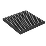
| 供应商器件封装 | 256-CSPBGA(17x17) |
| 包装 | 托盘 |
| 商标 | Analog Devices |
| 噪声系数 | - |
| 增益 | - |
| 安装风格 | SMD/SMT |
| 封装 | Tray |
| 封装/外壳 | 256-BGA,CSPBGA |
| 封装/箱体 | CSPBGA-256 |
| 射频 | 150 MHz |
| 工作电源电压 | 1.8 V |
| 工作电源电流 | 450 mA |
| 工厂包装数量 | 90 |
| 最大功率耗散 | 975 mW |
| 最大工作温度 | + 85 C |
| 最小工作温度 | - 40 C |
| 标准包装 | 1 |
| 混频器数 | 1 |
| 电压-电源 | 3 V ~ 3.6 V |
| 电流-电源 | 450mA |
| 系列 | AD6636 |
| 视频文件 | http://www.digikey.cn/classic/video.aspx?PlayerID=1364138032001&width=640&height=505&videoID=2245193150001 |
| 辅助属性 | 降频变频器 |
| 频率 | - |


- 商务部:美国ITC正式对集成电路等产品启动337调查
- 曝三星4nm工艺存在良率问题 高通将骁龙8 Gen1或转产台积电
- 太阳诱电将投资9.5亿元在常州建新厂生产MLCC 预计2023年完工
- 英特尔发布欧洲新工厂建设计划 深化IDM 2.0 战略
- 台积电先进制程称霸业界 有大客户加持明年业绩稳了
- 达到5530亿美元!SIA预计今年全球半导体销售额将创下新高
- 英特尔拟将自动驾驶子公司Mobileye上市 估值或超500亿美元
- 三星加码芯片和SET,合并消费电子和移动部门,撤换高东真等 CEO
- 三星电子宣布重大人事变动 还合并消费电子和移动部门
- 海关总署:前11个月进口集成电路产品价值2.52万亿元 增长14.8%


PDF Datasheet 数据手册内容提取
150 MSPS, Wideband, Digital Downconverter (DDC) AD6636 Synchronous serial I/O operation (SPI®-, SPORT-compatible) FEATURES Supports 8-bit or 16-bit microport modes 4/6 independent wideband processing channels 3.3 V I/O, 1.8 V CMOS core Processes 6 wideband carriers (UMTS, CDMA2000) User-configurable, built-in, self-test (BIST) capability 4 single-ended or 2 LVDS parallel input ports JTAG boundary scan (16 linear bit plus 3-bit exponent) running at 150 MHz APPLICATIONS Supports 300 MSPS input using external interface logic Three 16-bit parallel output ports operating up to 200 MHz Multicarrier, multimode digital receivers Real or complex input ports GSM, EDGE, PHS, UMTS, WCDMA, CDMA2000, TD-SCDMA, Quadrature correction and dc correction for complex inputs WiMAX Supports output rate up to 34 MSPS per channel Micro and pico cell systems, software radios RMS/peak power monitoring of input ports Broadband data applications Programmable attenuator control for external gain ranging Instrumentation and test equipment 3 programmable coefficient FIR filters per channel Wireless local loops 2 decimating half-band filters per channel In-building wireless telephony 6 programmable digital AGC loops with 96 dB range FUNCTIONAL BLOCK DIAGRAM FIR1 FIR2 MRCF CLKA NCO CIC5 HB1 HB2 DRCF CRCF LHB M = 1-32 M = 1-16 L = Byp, 2 M = Byp, 2 M = Byp, 2 M = 1-16 ADC A/AI X RI G T N EXPA [2:0] T MA NCO CIC5 FHIBR11 FHIBR22 MDRRCCFF CRCF LHB OUTI CLKB INPU M = 1-32 M = Byp, 2 M = Byp, 2 M = 1-16 M = 1-16 L = Byp, 2 ATA R PA ADC B/AQ D X RI CIC5 FIR1 FIR2 T MRCF CRCF LHB EXPB [2:0] NCO HB1 HB2 A DRCF M = 1-32 M = Byp, 2 M = Byp, 2 M M = 1-16 M = 1-16 L = Byp, 2 CMOS R CLKC REAL TE AGC PB PORTS U A, B, O ADC C/CI C, D NCO CIC5 FHIBR11 FHIBR22 A R MDRRCCFF CRCF LHB CMOS M = 1-32 M = Byp, 2 M = Byp, 2 AT M = 1-16 M = 1-16 L = Byp, 2 EXPC [2:0] COMPLEX D S PORTS T R (AI, AQ) O CLKD (BI, BQ) P PC CIC5 FIR1 FIR2 MRCF CRCF LHB EL ADC D/CQ PLOVRDTSS NCO M = 1-32 M =H BBy1p, 2 M =H BBy2p, 2 MD =R 1C-F16 M = 1-16 L = Byp, 2 ALL AB, CD R EXPD [2:0] A PEAK/ P RMS MEAS. RESET CIC5 FIR1 FIR2 MRCF CRCF LHB I,Q NCO M = 1-32 HB1 HB2 DRCF M = 1-16 L = Byp, 2 CORR. M = Byp, 2 M = Byp, 2 M = 1-16 SYNC [3:0] PRN GEN PLL CLOCK 16-BIT NOTE: CHANNELS RENDEREDM AUSLTIPLIER ARE AVAMILICARBOLEP OORNTL YIN ITNE 6R-CFAHCAENNEL PASRPTORT/SPI MIN T=E DREFCAIMCEATION L = JINTTAEGRPOLATION 04998-0-001 Figure 1. Rev. A Information furnished by Analog Devices is believed to be accurate and reliable. However, no responsibility is assumed by Analog Devices for its use, nor for any infringements of patents or other rights of third parties that may result from its use. One Technology Way, P.O. Box 9106, Norwood, MA 02062-9106, U.S.A. Specifications subject to change without notice. No license is granted by implication or otherwise under any patent or patent rights of Analog Devices. Trademarks and Tel: 781.329.4700 www.analog.com registered trademarks are the property of their respective owners. Fax: 781.461.3113 © 2005 Analog Devices, Inc. All rights reserved.
AD6636 TABLE OF CONTENTS General Description.........................................................................4 FIR Half-Band Block..................................................................30 Specifications.....................................................................................6 Intermediate Data Router.........................................................33 Recommended Operating Conditions......................................6 MonoRate RAM Coefficient Filter (MRCF)...........................33 Electrical Characteristics.............................................................6 Decimating RAM Coefficient Filter (DRCF).........................34 General Timing Characteristics, ................................................7 Channel RAM Coefficient Filter (CRCF)...............................36 Microport Timing Characteristics, ............................................8 Interpolating Half-Band Filter..................................................38 Serial Port Timing Characteristics, , ...........................................9 Output Data Router...................................................................38 Explanation of Test Levels for Specifications............................9 Automatic Gain Control............................................................40 Absolute Maximum Ratings..........................................................10 Parallel Port Output...................................................................44 Thermal Characteristics............................................................10 User-Configurable, Built-In Self-Test (BIST).........................48 ESD Caution................................................................................10 Chip Synchronization................................................................48 Pin Configuration and Function Descriptions...........................11 Serial Port Control.....................................................................49 Pin Listing for Power, Ground, Data, and Address Buses.....13 Microport....................................................................................58 Timing Diagrams............................................................................14 Memory Map..................................................................................60 Theory of Operation......................................................................20 Reading the Memory Map Table..............................................60 ADC Input Port..........................................................................20 Global Register Map..................................................................62 PLL Clock Multiplier.................................................................21 Input Port Register Map............................................................65 ADC Gain Control.....................................................................22 Channel Register Map...............................................................68 ADC Input Port Monitor Function..........................................23 Output Port Register Map.........................................................73 Quadrature I/Q Correction Block............................................25 Design Notes...................................................................................77 Input Crossbar Matrix...............................................................27 Outline Dimensions.......................................................................79 Numerically Controlled Oscillator (NCO).............................27 Ordering Guide..........................................................................79 Fifth-Order CIC Filter...............................................................29 Rev. A | Page 2 of 80
AD6636 REVISION HISTORY 6/05—Rev. 0 to Rev. A Changes to Desired Signal Level Mode Section..........................41 Changes to Format.............................................................Universal Changes to Figure 41......................................................................45 Changes to Figure 1...........................................................................1 Changes to Figure 42 and Figure 43.............................................46 Changes to Applications...................................................................1 Changes to Start with Soft Sync Section......................................48 Changes to General Description.....................................................4 Changes to Hop with Soft Sync Section.......................................49 Changes to Table 3............................................................................7 Changes to Hop with Pin Sync Section........................................49 Changes to Table 5............................................................................9 Replaced Serial Control Port Section...........................................49 Changes to Table 8..........................................................................11 Changes to Intel (INM) Mode Section.........................................58 Changes to Figure 17......................................................................18 Changes to Motorola (MNM) Mode Section..............................59 Changes to Figure 18 and Figure 19.............................................19 Changes to Table 30........................................................................61 Changes to Figure 25......................................................................23 Changes to Channel Register Map Section.................................68 Changes to Mean Power Mode (Control Bits 01) Section.........24 Changes to AGC Control Register <10:0> Section....................71 Changes to NCO Frequency Section............................................27 Changes to BIST Control <15:0> Section....................................73 Changes to Figure 30......................................................................28 Changes to Parallel Port Output Control <23:0>.......................73 Changes to 6-Tap Fixed Coefficient Filter (FIR2) Section........32 Changes to Table 44........................................................................74 Changes to Decimate-by-2, Half-Band Filter (HB2) Section....32 Changes to Design Notes...............................................................77 Changes to Table 17........................................................................32 Changes to Figure 59......................................................................77 Changes to Clock Rate Section......................................................34 Changes to Programming DRCF Register for a Symmetric Filter Section ...................................................................................35 8/04—Revision 0: Initial Version Changes to Channel RAM Coefficient Filter (CRCF) Section..............................................................................................36 Changes to Programming CRCF Register for a Symmetrical Filter Section....................................................................................37 Rev. A | Page 3 of 80
AD6636 GENERAL DESCRIPTION about 65 dB of rejection. The filters can be used either together The AD6636 is a digital downconverter intended for IF to achieve more than 95 dB stop band alias rejection, or can be sampling or oversampled baseband radios requiring wide individually bypassed to save power. FIR1 and HB1 filters can bandwidth input signals. The AD6636 has been optimized for run with a maximum input rate of 150 MSPS. In contrast, FIR2 the demanding filtering requirements of wideband standards, and HB2 can run with a maximum input rate of 75 MSPS (input such as CDMA2000, UMTS, and TD-SCDMA, but is flexible rate to FIR2 and HB2 filters). enough to support wider standards such as WiMAX. The AD6636 is designed for radio systems that use either an IF The programmable filtering is divided into three cascaded RAM sampling ADC or a baseband sampling ADC. coefficient filters (RCFs) for flexible and power efficient filtering. The first filter in the cascade is the MRCF, consisting The AD6636 channels have the following signal processing of a programmable nondecimating FIR. It is followed by stages: a frequency translator, a fifth-order cascaded integrated programmable FIR filters (DRCF) with decimation from 1 to comb filter, two sets of cascaded fixed-coefficient FIR and half- 16. They can be used either together to provide high rejection band filters, three cascaded programmable coefficient sum-of- filters, or independently to save power. The maximum input product FIR filters, an interpolating half-band filter (IHB), and rate to the MRCF is one-fourth of the PLL clock rate. a digital automatic gain control (AGC) block. Multiple modes are supported for clocking data into and out of the chip and The channel RCF (CRCF) is the last programmable FIR filter provide flexibility for interfacing to a wide variety of digitizers. with programmable decimation from 1 to 16. It typically is used Programming and control are accomplished via serial or to meet the spectral mask requirements for the air standard of microport interfaces. interest. This could be an RRC, antialiasing filter or any other real data filter. Decimation in preceding blocks is used to keep Input ports can take input data at up to 150 MSPS. Up to the input rate of this stage as low as possible for the best filter 300 MSPS input data can be supported using two input ports performance. (some external interface logic is required) and two internal channels processing in tandem. Biphase filtering in the output The last filter stage in the chain is an interpolate-by-2 half-band data router is selected to complete the combined filtering mode. filter, which is used to up-sample the CRCF output to produce The four input ports can operate in CMOS mode, or two ports higher output oversampling. Signal rejection requirements for can be combined for LVDS input mode. The maximum input this stage are relaxed because preceding filters have filtered the data rate for each input port is 150 MHz. blockers and adjacent carriers already. Frequency translation is accomplished with a 32-bit complex Each input port of the AD6636 has its own clock used for numerically controlled oscillator (NCO). It has greater than latching onto the input data, but the Input Port A clock (CLKA) 110 dBc SFDR. This stage translates either a real or complex is also used as the input for an on-board PLL clock multiplier. input signal from intermediate frequency (IF) to a baseband The output of the PLL clock is used for processing all filters and complex digital output. Phase and amplitude dither can be processing blocks beyond the data router following the CIC enabled on-chip to improve spurious performance of the NCO. filter. The PLL clock can be programmed to have a maximum A 16-bit phase-offset word is available to create a known phase clock rate of 200 MHz. relationship between multiple AD6636 chips or channels. The NCO can also be bypassed so that baseband I and Q inputs can A data routing block (DR) is used to distribute data from the be provided directly from baseband sampling ADCs through CICs to the various channel filters. This block allows multiple input ports. back-end filter chains to work together to process high bandwidth signals or to make even sharper filter transitions Following frequency translation is a fifth-order CIC filter with a than a single channel can perform. It can also allow complex programmable decimation between 1 and 32. This filter is used filtering operations to be achieved in the programmable filters. to lower the sample rate efficiently, while providing sufficient alias rejection at frequencies with higher frequency offsets from The digital AGC provides the user with scaled digital outputs the signal of interest. based on the rms level of the signal present at the output of the digital filters. The user can set the requested level and time Following the CIC5 are two sets of filters. Each set has a non- constant of the AGC loop for optimum performance of the decimating FIR filter and a decimate-by-2 half-band filter. The postprocessor. This is a critical function in the base station for FIR1 filter provides about 30 dB of rejection, while the HB1 CDMA applications where the power level must be well filter provides about 77 dB of rejection. They can be used controlled going into the RAKE receivers. It has programmable together to achieve a 107 dB stop band alias rejection, or they clipping and rounding control to provide different output can be individually bypassed to save power. The FIR2 filter resolutions. provides about 30 dB of rejection, while the HB2 filter provides Rev. A | Page 4 of 80
AD6636 PRODUCT HIGHLIGHTS The overall filter response for the AD6636 is the composite of • Six independent digital filtering channels all the combined filter stages. Each successive filter stage is capable of narrower transition bandwidths but requires a • 101 dB SNR noise performance, 110 dB spurious greater number of CLK cycles to calculate the output. More performance decimation in the first filter stage minimizes overall power • Four input ports capable of 150 MSPS input data rates consumption. Data from the device is interfaced to a DSP/FPGA/baseband processor via either high speed parallel • RMS/peak power monitoring of input ports and 96 dB ports (preferred) or a DSP-compatible microprocessor interface. range AGCs before the output ports The AD6636 is available both in 4-channel and 6-channel • Three programmable RAM coefficient filters, three half- versions. The data sheet primarily discusses the 6-channel part. band filters, two fixed coefficient filters, and one fifth- The only difference between the 6-channel and 4-channel order CIC filter per channel devices is that Channel 4 and Channel 5 are not available on the 4-channel version, (see Figure 1). The 4-channel device still has • Complex filtering and biphase filtering (300 MSPS ADC the same input ports, output ports, and memory map. The input) by combining filtering capability of multiple memory map section for Channel 4 and Channel 5 can be channels programmed and read back, but it serves no purpose. • Three 16-bit parallel output ports operating at up to a 200 MHz clock • Blackfin®-compatible and TigerSHARC®-compatible 16-bit microprocessor port • Synchronous serial communications port is compatible with most serial interface standards, SPORT, SPI, and SSR Rev. A | Page 5 of 80
AD6636 SPECIFICATIONS RECOMMENDED OPERATING CONDITIONS Table 1. Parameter Temp Test Level Min Typ Max Unit VDDCORE Full IV 1.7 1.8 1.9 V VDDIO Full IV 3.0 3.3 3.6 V T Full IV −40 +25 +85 °C AMBIENT ELECTRICAL CHARACTERISTICS1 Table 2. Parameter Temp Test Level Min Typ Max Unit LOGIC INPUTS (NOT 5 V TOLERANT) Logic Compatibility Full IV 3.3 V CMOS Logic 1 Voltage Full IV 2.0 3.6 V Logic 0 Voltage Full IV −0.3 +0.8 V Logic 1 Current Full IV 1 10 μA Logic 0 Current Full IV 1 10 μA Input Capacitance 25°C V 4 pF LOGIC OUTPUTS Logic Compatibility Full IV 3.3 V CMOS Logic 1 Voltage (I = 0.25 mA) Full IV 2.0 VDDIO − 0.2 V OH Logic 0 Voltage (I = 0.25 mA) Full IV 0.2 0.4 V OL SUPPLY CURRENTS WCDMA (61.44 MHz) Example1 I 25°C V 450 mA VDDCORE I 25°C V 50 mA VDDIO CDMA 2000 (61.44 MHz) Example1 I 25°C V 400 mA VDDCORE I 25°C V 25 mA VDDIO TDS-CDMA (76.8 MHz) Example1, 2 I 25°C V 250 mA VDDCORE I 25°C V 15 mA VDDIO GSM (65 MHz) Example1, 2 I 25°C V 175 mA VDDCORE I 25°C V 10 mA VDDIO TOTAL POWER DISSIPATION WCDMA (61.44 MHz)1 25°C V 975 mW CDMA2000 (61.44 MHz)1 25°C V 800 mW TD-SCDMA (76.8 MHz)1, 2 25°C V 500 mW GSM (65 MHz)1, 2 25°C V 350 mW 1 One input port, all six channels, and the relevant signal processing blocks are active. 2 PLL is turned off for power savings. Rev. A | Page 6 of 80
AD6636 GENERAL TIMING CHARACTERISTICS1, 2 Table 3. Parameter Temp Test Level Min Typ Max Unit CLK TIMING REQUIREMENTS t CLKx Period (x = A, B, C, D) Full I 6.66 ns CLK t CLKx Width Low (x = A, B, C, D) Full IV 1.71 0.5 × t ns CLKL CLK t CLKx Width High (x = A, B, C, D) Full IV 1.70 0.5 × t ns CLKH CLK t CLKA to CLKx Skew (x = B, C, D) Full IV t − 1.3 ns CLKSKEW CLK INPUT WIDEBAND DATA TIMING REQUIREMENTS Full IV tSI INx [15:0] to ↑CLKx Setup Time (x = A, B, C, D) Full IV 0.75 ns tHI INx [15:0] to ↑CLKx Hold Time (x = A, B, C, D) Full IV 1.13 ns tSEXP EXPx [2:0] to ↑CLKx Setup Time (x = A, B, C, D) Full IV 3.37 ns tHEXP EXPx [2:0] to ↑CLKx Hold Time (x = A, B, C, D) Full IV 1.11 ns tDEXP ↑CLKx to EXPx[2:0] Delay (x = A, B, C, D) Full IV 5.98 10.74 ns PARALLEL OUTPUT PORT TIMING REQUIREMENTS (MASTER) tDPREQ ↑PCLK to ↑Px REQ Delay (x = A, B, C) Full IV 1.77 3.86 ns tDPP ↑PCLK to Px [15:0] Delay (x = A, B, C) Full IV 2.07 5.29 ns tDPIQ ↑PCLK to Px IQ Delay (x = A, B, C) Full IV 0.48 5.49 ns tDPCH ↑PCLK to Px CH[2:0] Delay (x = A, B, C) Full IV 0.38 5.35 ns tDPGAIN ↑PCLK to Px Gain Delay (x = A, B, C) Full IV 0.23 4.95 ns tSPA Px ACK to ↑PCLK Setup Time (x = A, B, C) Full IV 4.59 ns tHPA Px ACK to ↑PCLK Hold Time (x = A, B, C) Full IV 0.90 ns PARALLEL OUTPUT PORT TIMING REQUIREMENTS (SLAVE) t PCLK Period Full IV 5.0 ns PCLK t PCLK Low Period Full IV 1.7 0.5 × t ns PCLKL PCLK t PCLK High Period Full IV 0.7 0.5 × t ns PCLKH PCLK tDPREQ ↑PCLK to ↑Px REQ Delay (x = A, B, C) Full IV 4.72 8.87 ns tDPP ↑PCLK to Px [15:0] Delay (x = A, B, C) Full IV 4.8 8.48 ns tDPIQ ↑PCLK to Px IQ Delay (x = A, B, C) Full IV 4.83 10.94 ns tDPCH ↑PCLK to Px CH[2:0] Delay (x = A, B, C) Full IV 4.88 10.09 ns tDPGAIN ↑PCLK to Px Gain Delay (x = A, B, C) Full IV 5.08 11.49 ns tSPA Px ACK to ↓PCLK Setup Time (x = A, B, C) Full IV 6.09 ns tHPA Px ACK to ↓PCLK Hold Time (x = A, B, C) Full IV 1.0 ns MISC PINS TIMING REQUIREMENTS t RESET Width Low Full IV 30 ns RESET t CPUCLK/SCLK to IRP Delay Full V 7.5 ns DIRP tSSYNC SYNC(0, 1, 2, 3) to ↑CLKA Setup Time Full IV 0.87 ns tHSYNC SYNC(0, 1, 2, 3) to ↑CLKA Hold Time Full IV 0.67 ns 1 All timing specifications are valid over the VDDCORE range of 1.7 V to 1.9 V and the VDDIO range of 3.0 V to 3.6 V. 2 CLOAD = 40 pF on all outputs, unless otherwise noted. Rev. A | Page 7 of 80
AD6636 MICROPORT TIMING CHARACTERISTICS1, 2 Table 4. Parameter Temp Test Level Min Typ Max Unit MICROPORT CLOCK TIMING REQUIREMENTS t CPUCLK Period Full IV 10.0 ns CPUCLK t CPUCLK Low Time Full IV 1.53 0.5 × t ns CPUCLKL CPUCLK t CPUCLK High Time Full IV 1.70 0.5 × t ns CPUCLKH CPUCLK INM MODE WRITE TIMING (MODE = 0) tSC Control3 to ↑CPUCLK Setup Time Full IV 0.80 ns tHC Control3 to ↑CPUCLK Hold Time Full IV 0.09 ns tSAM Address/Data to ↑CPUCLK Setup Time Full IV 0.76 ns tHAM Address/Data to ↑CPUCLK Hold Time Full IV 0.20 ns tDRDY ↑CPUCLK to RDY (DTACK) Delay Full IV 3.51 6.72 ns t Write Access Time Full IV 3 × t 9 × t ns ACC CPUCLK CPUCLK INM MODE READ TIMING (MODE = 0) tSC Control3 to ↑CPUCLK Setup Time Full IV 1.00 ns tHC Control3 to ↑CPUCLK Hold Time Full IV 0.03 ns tSAM Address to ↑CPUCLK Setup Time Full IV 0.80 ns tHAM Address to ↑CPUCLK Hold Time Full IV 0.20 ns tDD ↑CPUCLK to Data Delay Full V 5.0 ns tDRDY ↑CPUCLK to RDY (DTACK) Delay Full IV 4.50 6.72 ns t Read Access Time Full IV 3 × t 9 × t ns ACC CPUCLK CPUCLK MNM MODE WRITE TIMING (MODE = 1) tSC Control3 to ↑CPUCLK Setup Time Full IV 1.00 ns tHC Control3 to ↑CPUCLK Hold Time Full IV 0.00 ns tSAM Address/Data to ↑CPUCLK Setup Time Full IV 0.00 ns tHAM Address/Data to ↑CPUCLK Hold Time Full IV 0.57 ns tDDTACK ↑CPUCLK to DTACK (RDY) Delay Full IV 4.10 5.72 ns t Write Access Time Full IV 3 × t 9 × t ns ACC CPUCLK CPUCLK MNM MODE READ TIMING (MODE = 1) tSC Control3 to ↑CPUCLK Setup Time Full IV 1.00 ns tHC Control3 to ↑CPUCLK Hold Time Full IV 0.00 ns tSAM Address to ↑CPUCLK Setup Time Full IV 0.00 ns tHAM Address to ↑CPUCLK Hold Time Full IV 0.57 ns t CPUCLK to Data Delay Full V 5.0 ns DD tDDTACK ↑CPUCLK to DTACK (RDY) Delay Full IV 4.20 6.03 ns t Read Access Time Full IV 3 × t 9 × t ns ACC CPUCLK CPUCLK 1 All timing specifications are valid over the VDDCORE range of 1.7 V to 1.9 V and the VDDIO range of 3.0 V to 3.6 V. 2 CLOAD = 40 pF on all outputs, unless otherwise noted. 3 Specification pertains to control signals: R/W (WR), DS (RD), and CS. Rev. A | Page 8 of 80
AD6636 SERIAL PORT TIMING CHARACTERISTICS1, 2, 3 Table 5. Parameter Temp Test Level Min Typ Max Unit SERIAL PORT CLOCK TIMING REQUIREMENTS t SCLK Period Full IV 10.0 ns SCLK t SCLK Low Time Full IV 1.60 0.5 × t ns SCLKL SCLK t SCLK High Time Full IV 1.60 0.5 × t ns SCLKH SCLK SPI PORT CONTROL TIMING REQUIREMENTS (MODE = 0) tSSDI SDI to ↑SCLK Setup Time Full IV 1.30 ns tHSDI SDI to ↑SCLK Hold Time Full IV 0.40 ns tSSCS SCS to ↑SCLK Setup Time Full IV 4.12 ns tHSCS SCS to ↑SCLK Hold Time Full IV −2.78 ns tDSDO ↑SCLK to SDO Delay Time Full IV 4.28 7.96 ns SPORT MODE CONTROL TIMING REQUIREMENTS (MODE = 1) tSSDI SDI to ↑SCLK Setup Time Full IV 0.80 ns tHSDI SDI to ↑SCLK Hold Time Full IV 0.40 ns tSSRFS SRFS to ↓SCLK Setup Time Full IV 1.60 ns tHSRFS SRFS to ↓SCLK Hold Time Full IV −0.13 ns tSSTFS STFS to ↓SCLK Setup Time Full IV 1.60 ns tHSTFS STFS to ↑SCLK Hold Time Full IV −0.30 ns tSSCS SCS to ↑SCLK Setup Time Full IV 4.12 ns tHSCS SCS to ↑SCLK Hold Time Full IV −2.76 ns tDSDO ↑SCLK to SDO Delay Time Full IV 4.29 7.95 ns 1 All timing specifications are valid over the VDDCORE range of 1.7 V to 1.9 V and the VDDIO range of 3.0 V to 3.6 V. 2 CLOAD = 40 pF on all outputs, unless otherwise noted. 3 SCLK rise/fall time should be 3 ns maximum. EXPLANATION OF TEST LEVELS FOR SPECIFICATIONS Table 6. Test Level Description I 100% production tested. II 100% production tested at 25°C, and sample tested at specified temperatures. III Sample tested only. IV Parameter guaranteed by design and analysis. V Parameter is typical value only. VI 100% production tested at 25°C, and sampled tested at temperature extremes. Rev. A | Page 9 of 80
AD6636 ABSOLUTE MAXIMUM RATINGS Table 7. Parameter Rating Stresses above those listed under the Absolute Maximum ELECTRICAL Ratings may cause permanent damage to the device. This is a VDDCORE Supply Voltage 2.2 V stress rating only; functional operation of the device at these or (Core Supply) any other conditions above those indicated in the operational VDDIO Supply Voltage 4.0 V section of this specification is not implied. Exposure to absolute (Ring or IO Supply) maximum rating conditions for extended periods may affect Input Voltage −0.3 to +3.6 V (Not 5 V Tolerant) device reliability. Output Voltage −0.3 to VDDIO + 0.3 V Load Capacitance 200 pF THERMAL CHARACTERISTICS ENVIRONMENTAL 256-ball CSP_BGA package: Operating Temperature −40°C to +85°C Range (Ambient) θ = 25.4°C /W, no airflow JA Maximum Junction 125°C Temperature Under Bias θ = 23.3°C /W, 0.5 m/s airflow JA Storage Temperature −65°C to +150°C Range (Ambient) θJA = 22.6°C /W, 1.0 m/s airflow θ = 21.9°C /W, 2.0 m/s airflow JA Thermal measurements made in the horizontal position on a 4-layer board with vias. ESD CAUTION ESD (electrostatic discharge) sensitive device. Electrostatic charges as high as 4000 V readily accumulate on the human body and test equipment and can discharge without detection. Although this product features proprietary ESD protection circuitry, permanent damage may occur on devices subjected to high energy electrostatic discharges. Therefore, proper ESD precautions are recommended to avoid performance degradation or loss of functionality. Rev. A | Page 10 of 80
AD6636 PIN CONFIGURATION AND FUNCTION DESCRIPTIONS 1 2 3 4 5 6 7 8 9 10 11 12 13 14 15 16 A GND INC3 IND4 IND7 CLKD CLKC IND11 GND VDDCORE IND14 IND15 SYNC1 TDO PBGAIN PB11 GND A B IND0 VDDIO INC2 IND5 IND6 IND8 IND10 IND12 IND13 INC14 SYNC3 SYNC0 TRST PBCH2 VDDIO PB12 B C EXPA1 EXPD1 INC0 INC1 IND3 INC5 IND9 INC10 INC13 SYNC2 TMS TCLK PBCH0 PB8 PB15 PB10 C D EXPB0 EXPC2 EXPC1 EXPD0 IND2 INC4 INC7 INC9 INC12 TDI PBCH1 PBIQ PB14 PB9 PB13 PACH1 D LVDS_ E INA14 INA15 EXPA0 RSET GND IND1 INC6 INC8 INC11 INC15 PBREQ PBACK PB4 PB5 PB1 PCLK E F INA12 INA13 EXPB1 EXPC0 EXPD2 GND VDDIO VDDIO VDDIO VDDIO GND PB6 PB0 PB7 PAREQ PA0 F G INA11 INB13 INB15 EXPB2 EXPA2 VDDCORE GND GND GND GND VDDCORE PB3 PAGAIN PB2 PACH0 PA2 G H VDDCORE INA10 INB12 INB11 INB14 VDDCORE GND GND GND GND VDDCORE PACH2 PAIQ PAACK PA1 GND H J GND INA9 INB10 INB8 INB9 VDDCORE GND GND GND GND VDDCORE PA3 PA7 PA5 PA4 VDDCORE J K CLKA INA8 INA7 INB6 INB7 VDDCORE GND GND GND GND VDDCORE PA12 PA15 PA9 PA8 PA6 K L CLKB INA6 INB4 INB1 INB3 GND VDDIO VDDIO VDDIO VDDIO GND PC3 PCACK PCCH1 PA13 PA10 L M INA5 INB5 INB2 INB0 GND DTACK D13 D15 D5 A5 PC12 PC7 PC2 PC0 PCCH0 PA11 M (RDY, SDO) N INA4 INA3 INA0 R/W (WR, CS (SCS) CHIPID2 D12 D2 D1 A4 A0 (SDI) PC15 PC5 PC1 PCCH2 PA14 N STFS) P INA2 INA1 RESET DS (RD, SMODE CHIPID3 GND D9 D4 A6 A2 PC11 PC10 PC4 PCIQ PCGAIN P SRFS) R CPUCLK VDDIO MSB_ EXT_ CHIPID1 D14 D10 D11 D6 D0 A3 A1 PC9 PC6 VDDIO PCREQ R (SCLK) FIRST FILTER T GND IRP MODE CHIPID0 D7 D8 D3 VDDCORE GND GND A7 PC14 PC13 PC8 GND GND T 1 2 3 4 5 6 7 8 9 10 11 12 13 14 15 16 = VDDCORE = VDDIO = GROUND 04998-0-002 Figure 2. CSP_BGA Pin Configuration Table 8. Pin Function Descriptions Mnemonic Type Pin No. Function POWER SUPPLY VDDCORE Power See Table 9 1.8 V Digital Core Supply. VDDIO Power See Table 9 3.3 V Digital I/O Supply. GND Ground See Table 9 Digital Core and I/O Ground. INPUT (ADC) PORTS (CMOS/LVDS) CLKA Input K1 Clock for Input Port A. Used to clock INA[15:0] and EXPA[2:0] data. Additionally, this clock is used to drive internal circuitry and PLL clock multiplier. CLKB Input L1 Clock for Input Port B. Used to clock INB[15:0] and EXPB[2:0] data. CLKC Input A6 Clock for Input Port C. Used to clock INC[15:0] and EXPC[2:0] data. CLKD Input A5 Clock for Input Port D. Used to clock IND[15:0] and EXPD[2:0] data. INA[0:15] Input See Table 9 Input Port A (Parallel). INB[0:15] Input See Table 9 Input Port B (Parallel). INC[0:15] Input See Table 9 Input Port C (Parallel). IND[0:15] Input See Table 9 Input Port D (Parallel). EXPA[0:2] Bidirectional E3, C1, G5 Exponent Bus Input Port A. Gain control output. Rev. A | Page 11 of 80
AD6636 Mnemonic Type Pin No. Function EXPB[0:2] Bidirectional D1, F3, G4 Exponent Bus Input Port B. Gain control output. EXPC[0:2] Bidirectional F4, D3, D2 Exponent Bus Input Port C. Gain control output. EXPD[0:2] Bidirectional D4, C2, F5 Exponent Bus Input Port D. Gain control output. CLKA, CLKB Input K1, L1 LVDS Differential Clock for LVDS_A Input Port (LVDS_CLKA+, LVDS_CLKA−). CLKC, CLKD Input A6, A5 LVDS Differential Clock for LVDS_C Input Port (LVDS_CLKC+, LVDS_CLKC−). INA[0:15], LVDS Input See Table 9 In LVDS input mode, INA[0:15] and INB[0:15] form a differential pair LVDS_A+[0:15] INB[0:15] (positive node) and LVDS_A–[0:15] (negative node), respectively. INC[0:15], LVDS Input See Table 9 In LVDS input mode, INC[0:15] and IND[0:15] form a differential pair LVDS_C+[0:15] IND[0:15] (positive node) and LVDS_C–[0:15] (negative node), respectively. OUTPUT PORTS PCLK Bidirectional E16 Parallel Output Port Clock. Master mode output, and slave mode input. PA[0:15] Output See Table 9 Parallel Output Port A Data Bus. PACH[0:2] Output G15, D16, Channel Indicator Output Port A. H12 PAIQ Output H13 Parallel Port A I/Q Data Indicator. Logic 1 indicates I data on data bus. PAGAIN Output G13 Parallel Port A Gain Word Output Indicator. Logic 1 indicates gain word on data bus. PAACK Input H14 Parallel Port A Acknowledge (Active High). PAREQ Output F15 Parallel Port A Request (Active High). PB[0:15] Output See Table 9 Parallel Output Port B Data Bus. PBCH[0:2] Output C13, D11, Channel Indicator Output Port B. B14 PBIQ Output D12 Parallel Port B I/Q Data Indicator. Logic 1 indicates I data on data bus. PBGAIN Output A14 Parallel Port B Gain Word Output Indicator. Logic 1 indicates gain word on data bus. PBACK Input E12 Parallel Port B Acknowledge (Active High). PBREQ Output E11 Parallel Port B Request (Active High). PC[0:15] Output See Table 9 Parallel Output Port C Data Bus. PCCH[0:2] Output M15, L14, Channel Indicator Output Port C. N15 PCIQ Output P15 Parallel Port C I/Q Data Indicator. Logic 1 indicates I data on data bus. PCGAIN Output P16 Parallel Port C Gain Word Output Indicator. Logic 1 indicates gain word on data bus. PCACK Input L13 Parallel Port C Acknowledge (Active High). PCREQ Output R16 Parallel Port C Request (Active High). MISC PINS RESET Input P3 Master Reset (Active Low). IRP1 Output T2 Interrupt Pin (Open Drain Output, Needs External Pull-Up Resistor 1 kΩ). SYNC[0:3] Input B12, A12, Synchronization Inputs. SYNC pins are independent of channels or input ports and C10, B11 independent of each other. LVDS_RSET Input E4 LVDS Resistor Set Pin (Analog Pin). See Design Notes. EXT_FILTER Input R4 PLL Loop Filter (Analog Pin). See Design Notes. MICROPORT CONTROL D[0:15] Bidirectional See Table 9 Bidirectional Microport Data. This bus is three-stated when CS is high. A[0:7] Input See Table 9 Microport Address Bus. DS (RD) Input P4 Active Low Data Strobe when MODE = 1. Active low read strobe when MODE = 0. DTACK (RDY)1 Output M6 Active Low Data Acknowledge when MODE = 1. Microport status pin when MODE = 0. Open drain output, needs external pull-up resistor 1 kΩ. R/W (WR) Input N4 Read/Write Strobe when MODE = 1. Active low write strobe when MODE = 0. MODE Input T3 Mode Select Pin. When SMODE = 0: Logic 0 = Intel mode; Logic 1 = Motorola mode. When SMODE = 1: Logic 0 = SPI mode; Logic 1 = SPORT mode. CS Input N5 Active Low Chip Select. Logic 1 three-states the microport data bus. CPUCLK Input R1 Microport CLK Input (Input Only). CHIPID[0:3] Input T4, R5, N6, Chip ID Input Pins. P6 Rev. A | Page 12 of 80
AD6636 Mnemonic Type Pin No. Function SERIAL PORT CONTROL SCLK Input R1 Serial Clock. SDO1 Output M6 Serial Port Data Output (Open drain output, needs external pull-up resistor 1KΩ). SDI2 Input N11 Serial Port Data Input. STFS Input N4 Serial Transmit Frame Sync. SRFS Input P4 Serial Receive Frame Sync. SCS Input N5 Serial Chip Select. MSB_FIRST Input R3 Select MSB First into SDI Pin and MSB First Out of SDO Pin. Logic 0 = MSB first; Logic 1 = LSB first. SMODE Input P5 Serial Mode Select. Pull high when serial port is used and low when microport is used. JTAG TRST1 Input B13 Test Reset Pin. Pull low when JTAG is not used. TCLK2 Input C12 Test Clock. TMS1 Input C11 Test Mode Select. TDO Output A13 Test Data Output. Three-stated when JTAG is in reset. TDI1 Input D10 Test Data Input. 1 Pin with a pull-up resistor of nominal 70 kΩ. 2 Pin with a pull-down resistor of nominal 70 kΩ. PIN LISTING FOR POWER, GROUND, DATA, AND ADDRESS BUSES Table 9. Mnemonic Pin No. VDDCORE A9, G6, G11, H1, H6, H11, J6, J11, J16, K6, K11, T8 VDDIO B2, B15, F7, F8, F9, F10, L7, L8, L9, L10, R2, R15 GND A1, A8, A16, E5, F6, F11, G7, G8, G9, G10, H7, H8, H9, H10, H16, J1, J7, J8, J9, J10, K7, K8, K9, K10, L6, L11, M5, P7, T1, T9, T10, T15, T16 INA[0:15] N3, P2, P1, N2, N1, M1, L2, K3, K2, J2, H2, G1, F1, F2, E1, E2 INB[0:15] M4, L4, M3, L5, L3, M2, K4, K5, J4, J5, J3, H4, H3, G2, H5, G3 INC[0:15] C3, C4, B3, A2, D6, C6, E7, D7, E8, D8, C8, E9, D9, C9, B10, E10 IND[0:15] B1, E6, D5, C5, A3, B4, B5, A4, B6, C7, B7, A7, B8, B9, A10, A11 PA[0:15] F16, H15, G16, J12, J15, J14, K16, J13, K15, K14, L16, M16, K12, L15, N16, K13 PB[0:15] F13, E15, G14, G12, E13, E14, F12, F14, C14, D14, C16, A15, B16, D15, D13, C15 PC[0:15] M14, N14, M13, L12, P14, N13, R14, M12, T14, R13, P13, P12, M11, T13, T12, N12 D[0:15] R10, N9, N8, T7, P9, M9, R9, T5, T6, P8, R7, R8, N7, M7, R6, M8 A[0:7] N11, R12, P11, R11, N10, M10, P10, T11 Rev. A | Page 13 of 80
AD6636 TIMING DIAGRAMS RESET tRESL 04998-0-003 Figure 3. Reset Timing Requirements t CLKH CLKx tCLKL 04998-0-004 Figure 4. CLK Switching Characteristics (x = A, B, C, D for Individual Input Ports) t CLK t CLKL CLKA t CLKH t CLKSKEW CLKx 04998-0-005 Figure 5. CLK Skew Characteristics (x = B, C, D for Individual Input Ports) t CPUCLKH CPUCLK tCPUCLKL 04998-0-006 Figure 6. CPUCLK Switching Characteristics t SCLKH SCLK tSCLKL 04998-0-007 Figure 7. SCLK Switching Characteristics CLKA t t SSYNC HSYNC SYNC [3:0] 04998-0-008 Figure 8. SYNC Timing Inputs Rev. A | Page 14 of 80
AD6636 t CLK t CLKL CLKx t CLKH t DEXP EXPx[2:0] 04998-0-009 Figure 9. Gain Control Word Output Switching Characteristics (x = A, B, C, D for Individual Input Ports) CLKx t t SI HI INx[15:0] t t SEXP HEXP EXPx[15:0] 04998-0-010 Figure 10. Input Port Timing for Data (x = A, B, C, D for Individual Input Ports) PCLK tSPA tHPA PxACK t DPREQ PxREQ t t t t DPP DPP t DPP DPP t DPP DPP Px [15:0] I [15:0] Q [15:0] RSSI [11:0] I [15:0] Q [15:0] RSSI [11:0] PxIQ tDPIQ tDPIQ t t DPCH DPCH PxCH [2:0] PxCH [2:0] = CHANNEL # PxCH [2:0] = CHANNEL # PxGAIN tDPGAIN tDPGAIN 04998-0-011 Figure 11. Master Mode PxACK to PCLK Switching Characteristics (x = A, B, C, D for Individual Output Ports) Rev. A | Page 15 of 80
AD6636 PCLK PxACK TIED LOGIC HIGH ALL THE TIME t DPREQ PxREQ t t t t t t DPP DPP DPP DPP DPP DPP Px [15:0] I [15:0] Q [15:0] RSSI [11:0] I [15:0] Q [15:0] RSSI [11:0] PxIQ tDPIQ tDPIQ t t DPCH DPCH PxCH [2:0] PxCH [2:0] = CHANNEL # PxCH [2:0] = CHANNEL # PxGAIN tDPGAIN tDPGAIN 04998-0-012 Figure 12. Master Mode PxREQ to PCLK Switching Characteristics CPUCLK RD t t SC HC WR t t SC HC CS t t SAM HAM A [7:0] VALID ADDRESS t t SAM HAM D [15:0] VALID DATA t DRDY RDY t ACC NtAOCTCE A:CCESS TIME DEPENDS ON THE ADDRESS ACCESSED. IT CAN VARY FROM 3 TO 9 CPUCLK CYCLES. 04998-0-013 Figure 13. INM Microport Write Timing Requirements Rev. A | Page 16 of 80
AD6636 CPUCLK t HC t SC RD WR t HC t SC CS t SAM t HAM A [7:0] VALID ADDRESS t DD D [15:0] VALID DATA t DRDY RDY t ACC NtAOCTCE A:CCESS TIME DEPENDS ON THE ADDRESS ACCESSED. IT CAN VARY FROM 3 TO 9 CPUCLK CYCLES. 04998-0-014 Figure 14. INM Microport Read Timing Requirements CPUCLK tSC tHC DS t t SC HC R/W tSC tHC CS tSAM tHAM A [7:0] VALID ADDRESS t t SAM HAM D [15:0] VALID DATA t DDTACK DTACK t ACC NtAOCTCE A:CCESS TIME DEPENDS ON THE ADDRESS ACCESSED. IT CAN VARY FROM 3 TO 9 CPUCLK CYCLES. 04998-0-015 Figure 15. MNM Microport Write Timing Requirements Rev. A | Page 17 of 80
AD6636 CPUCLK tSC tHC DS t t SC HC R/W t t SC HC CS tSAM tHAM A [7:0] VALID ADDRESS t DD VALID D [15:0] DATA t DDTACK DTACK t ACC NtAOCTCE A:CCESS TIME DEPENDS ON THE ADDRESS ACCESSED. IT CAN VARY FROM 3 TO 9 CPUCLK CYCLES. 04998-0-016 Figure 16. MNM Microport Read Timing Requirements SCLK t SSCS t HSCS SCS SMODE LOGIC 1 t HSDI t SSDI SDI D0 D1 D2 D3 D4 D5 D6 D7 t t HSRFS SSRFS SRFS MODE LOGIC 1 04998-0-017 Figure 17. SPORT Mode Write Timing Characteristics Rev. A | Page 18 of 80
AD6636 SCLK t SSCS t HSCS SCS SMODE LOGIC 1 t DSDO SDO D0 D1 D2 D3 D4 D5 D6 D7 t HSTFS t SSTFS STFS MODE LOGIC 1 04998-0-018 Figure 18. SPORT Mode Read Timing Characteristics SCLK t t SSCS HSCS SCS SMODE LOGIC 1 t HSDI t SSDI SDI D0 D1 D2 D3 D4 D5 D6 D7 MODE LOGIC 0 04998-0-019 Figure 19. SPI Mode Write Timing Characteristics SCLK t t SSCS HSCS SCS SMODE LOGIC 0 t DSDO SDO D0 D1 D2 D3 D4 D5 D6 D7 MODE LOGIC 0 04998-0-020 Figure 20. SPI Mode Read Timing Characteristics Rev. A | Page 19 of 80
AD6636 THEORY OF OPERATION ADC INPUT PORT The 3-exponent bits are shared with the gain range control bits in the hardware. When floating-point ADCs are not used, these The AD6636 features four identical, independent high speed three pins on each ADC input port can be used as gain range ADC input ports named A, B, C, and D. These input ports have control output bits. the flexibility to allow independent inputs, diversity inputs, or complex I/Q inputs. Any of the ADC input ports can be routed Input Timing to any of the six tuner channels; that is, any of the six. The The data from each high speed input port is latched either on AD6636 channels can receive input data from any of the input the rising edge or the falling edge of the port’s individual CLKx ports. Time-multiplexed inputs on a single port are not (where x stands for A, B, C, or D input ports). The ADC clock supported in the AD6636. invert bit in ADC clock control register selects the edge of the These four input ports can operate at up to 150 MSPS. Each clock (rising or falling) used to register input data into the input port has its own clock (CLKA, CLKB, CLKC, and CLKD) AD6636. used for registering input data into the AD6636. To allow slow input rates while providing fast processing clock rates, the CLKx AD6636 contains an internal PLL clock multiplier that supplies t t the internal signal processing clock. CLKA is used as an input SI HI ttoh et hinep PuLtL d caltoa ctko mbeu cltliopclkieerd. Aindtdoi ttihoen paal rptr eoigthraemr omna tbhilei tryi sailnlogw s EIXNPx x[ 1[52::00]] DATA n DATA n + 1 04998-0-021 edge or the falling edge of the input clock. Figure 21. Input Data Timing Requirements (Rising Edge of Clock, x = A, B, C, or D for Four Input Ports) In addition, the front end of the AD6636 contains circuitry that enables high speed signal-level detection, gain control, and quadrature I/Q correction. This is accomplished with a unique CLKx high speed level-detection circuit that offers minimal latency and maximum flexibility to control all four input signals tSI tHI (ptryopviicdaell yin ApuDtC p oinwpeur-tsm) oinnditiovridinuga lfluy.n Tcthioe nins pvuiat vpaorritosu asl smo odes EIXNPx x[ 1[52::00]] DATA n DATA n + 1 04998-0-022 and magnitude and phase I/Q correction blocks. See the Figure 22. Input Data Timing Requirements Quadrature I/Q Correction Block section for details. (Falling Edge of Clock, x = A, B, C, or D for Four Input Ports) Each individual processing channel can receive input data from The clock signals (CLKA, CLKB, CLKC, and CLKD) can any of the four input ports individually. This is controlled using operate at up to 150 MHz. In applications using high speed 3-bit crossbar mux-select bit words in the ADC input control ADCs, the ADC sample clock, data valid, or data-ready strobe register. Each individual channel has a similar 3-bit selection. In are typically used to clock the AD6636. addition to the four input ports, an internal test signal (PN— Connection to Fixed-Point ADC pseudorandom noise sequence) can also be selected. This internal test signal is discussed in the User-Configurable, Built- For fixed-point ADCs, the AD6636 exponent inputs, EXP[2:0], In Self-Test (BIST) section. are not typically used and should be tied low. Alternatively, because these pins are shared with gain range control bits, if the Input Data Format gain ranging block is used, these pins can be used as outputs of Each input port consists of a 16-bit mantissa and a 3-bit the gain range control block. The ADC outputs are tied directly exponent (16 + 3 floating-point input, or up to 16-bit fixed- to the AD6636 inputs, MSB justified. Therefore, for fixed-point point input). When interfacing to standard fixed-point ADCs, ADCs, the exponents are typically static and no input scaling is the exponent bit should either be connected to ground or be used in the AD6636. Figure 23 shows a typical interconnection. programmed as outputs for gain control output. If connected to a floating-point ADC (also called gain ranging ADC), the exponent bits from the ADC can be connected to the input exponent bits of the AD6636. The mantissa data format is twos complement, and the exponent is unsigned binary. Rev. A | Page 20 of 80
AD6636 D13 (MSB) IN15 indicate Input Port A, and the complex input bit should be selected. AD6645 14-BIT ADC When the input ports are paired for complex input operation, AD6636 only one set of exponent bits is driven externally with gain control output. Therefore, when Input Port A and Input Port B form a complex input, EXPA[2:0] are output and, similarly, for Input Port C and Input Port D, EXPC[2:0] are output. D0 (LSB) IN2 IN1 LVDS Input Ports IN0 The AD6636 input ports can be configured in CMOS mode or GAIN BRIATSNE GOXIRPN OGGN RCEOONUNTNT BRDIOETDSL EEEXXXPPP012 04998-0-023 LcoVnDfiSg umreodd ea.s I tnw Co McoOmSp ilnexp uint pmuot dpeo,r tths.e I fno uLVr iDnpSu mt podoret, st wcaon C bMe OS Figure 23. Typical Interconnection of the AD6645 Fixed-Point ADC and AD6636 input ports are each combined to form one LVDS input port. Scaling with Floating-Point ADC CMOS Input Port INA[15:0] and CMOS Input Port INB[15:0] An example of the exponent control feature combines the form the positive and negative differential nodes, AD6600 and the AD6636. The AD6600 is an 11-bit ADC with LVDS_A+[15:0] and LVDS_A−[15:0], respectively. Similarly, three bits of gain ranging. In effect, the 11-bit ADC provides the INC[15:0] and IND[15:0] form the positive and negative mantissa, and the three bits of the relative signal strength differential nodes, LVDS_C+[15:0] and LVDS_C− [15:0], indicator (RSSI) are the exponent. Only five of the eight respectively. CLKA and CLKB form the differential pair, available steps are used by the AD6600. See the AD6600 data Pin LVDS_CLKA+ and Pin LVDS_CLKA−. Similarly, CLKC sheet for details. and CLKD form the differential pair Pin LVDS_CLKC+ and Table 10. Weighting Factors for Different Exp[2:0] Values Pin LVDS_CLKC−. ADC Input AD6636 Data Signal By default, the AD6636 powers up in CMOS mode and can be Level Exp[2:0] Divide-By Attenuation (dB) programmed to CMOS mode by using the CMOS mode bit Largest 000 (0) /1 (>> 0) 0 (Bit 10 of the LVDS control register). Writing Logic 1 to Bit 8 of 001 (1) /2 (>> 1) 6 the LVDS control register enables an autocalibrate routine that 010 (2) /4 (>> 2) 12 calibrates the impedance of the LVDS pads to match the output 011 (3) /8 (>> 3) 18 impedance of the LVDS signal source impedance. The LVDS pads 100 (4) /16 (>> 4) 24 in the AD6636 have an internal impedance of 100 Ω across the 101 (5) /32 (>> 5) 30 differential signals; therefore, an external resistor is not required. 110 (6) /64 (>> 6) 36 Smallest 111 (7) /128 (>> 7) 42 PLL CLOCK MULTIPLIER In the AD6636, the input clock rate must be the same as the Complex (I/Q) Input Ports input data rate. In a typical digital downconverter architecture, The four individual ADC input ports of the AD6636 can be the clock rate is a limitation on the number of filter taps that configured to function as two complex input ports. can be calculated in the programmable RAM coefficient filters Additionally, if required, only two input ports can be made to (MRCF, DRCF, and CRCF). For slower ADC clock rates (or for function as a complex port, while the remaining two input ports any clock rate), this limitation can be overcome by using a PLL function as real individual input ports. clock multiplier to provide a higher clock rate to the RCF filters. Using this clock multiplier, the internal signal processing clock In complex mode, Input Port A is paired with Input Port B to rate can be increased up to 200 MHz. The CLKA signal is used receive I and Q data, respectively. Similarly, Input Port C can be as an input to the PLL clock multiplier. paired with Input Port D to receive I and Q data, respectively. These two pairings are controlled individually using Bit 24 and PLL CLOCK GENERATION Bit 25 of the ADC input control register. 1 ADC_CLK 0 As explained previously, each individual channel can receive input signals from any of the four input ports using the crossbar CLKA (D1I,V 2ID, 4E OBRY 8N) MPLULL ICTLPOLCIEKR 0 PLL_CLK mux select bits in the ADC input control register. In addition to (4x TO 20x) 1 the three bits, a 1-bit selection is provided for choosing the BYPASS_PLL ceoxammpplelex, iinf pCuht apnonret lo 0p ntieoend fso tro a rneyc einivdei vcoidmupall ecxh iannpnuetl .f Froomr N2 M5 1 FOR BYPASS 04998-0-024 Input Port A and Input Port B, the mux select bits should Figure 24. PLL Clock Generation Rev. A | Page 21 of 80
AD6636 The PLL clock multiplier is programmable and uses input clock Function rates between 4 MHz and 150 MHz to give a system clock rate The gain-control block features a programmable upper (output) of as high as 200 MHz. threshold register and a lower threshold register. The ADC input data is compared to both these registers. If ADC input The output clock rate is given by data is larger than the upper threshold register, then the gain CLKA×M control output is decremented by 1. If ADC input data is PLL_CLK= N smaller than the lower threshold register, then the gain control output is incremented by 1. When decrementing the gain where: control output, the change is immediate. But when incrementing the output, a dwell-time register is used to delay CLKA is the Input Port A clock rate. the change. If the ADC input is larger than the upper threshold M is a 5-bit programmable multiplication factor. register value, the gain-control output is decremented to prevent overflow immediately. N is a predivide factor. When the ADC input is lower than the lower threshold register, M is a 5-bit number between 4 and 20 (both values included). N a dwell timer is loaded with the value in the programmable, (predivide) can be 1, 2, 4, or 8. The multiplication factor M is 20-bit, dwell-time register. The counter decrements once every programmed using a 5-bit PLL clock multiplier word in the input clock cycle, as long as the input signal remains below the ADC clock control register. A value outside the valid range of 4 lower threshold register value. If the counter reaches 1, the gain to 20 bypasses the PLL clock multiplier and, therefore, the PLL control output is incremented by 1. If the signal goes above the clock is the same as the input clock. The predivide factor N is lower threshold register value, the gain adjustment is not made, programmed using a 2-bit ADC pre-PLL clock divider word in and the normal comparison to lower and upper threshold the ADC clock control register, as listed in Table 11. registers is initiated once again. Therefore, the dwell timer Table 11. PLL Clock Generation Predivider Control provides temporal hysteresis and prevents the gain from Predivide Word [1:0] Divide-by Value for the Clock switching continuously. 00 Divide-by-1, bypass In a typical application, if the ADC signal goes below the lower 01 Divide-by-2 threshold for a time greater than the dwell time, then the gain 10 Divide-by-4 control output is incremented by 1. Gain control bits control the 11 Divide-by-8 gain ranging block, which appears before the ADC in the signal For the best signal processing advantage, the user should chain. With each increment of the gain control output, gain in program the clock multiplier to give a system clock output as the gain-ranging block is increased by 6.02 dB. This increases close as possible to, but not exceeding, 200 MHz. The internal the dynamic range of the input signal into the ADC by 6.02 dB. blocks of the AD6636 that run off of the PLL clock are rated to This gain is compensated for in the AD6636 by relinearizing run at a maximum of 200 MHz. The default power-up state for (see the Relinearization section). Therefore, the AD6636 can the PLL clock multiplier is the bypass state, where CLKA is increase the dynamic range of the ADC by 42 dB, provided that passed on as the PLL clock. the gain-ranging block can support it. ADC GAIN CONTROL Relinearization Each ADC input port has individual, high speed, gain-control The gain in the gain-ranging block (external) is compensated logic circuitry. Such gain-control circuitry is useful in applica- for by relinearizing, using the exponent bits, EXP[2:0], of the tions that involve large dynamic range inputs or in which gain input port. For this purpose, the gain control bits are connected ranging ADCs are employed. The AD6636 gain-control logic to the EXP[2:0] bits, providing an attenuation of 6.02 dB for allows programmable upper and lower thresholds and a every increase in the gain control output. After the gain in the programmable dwell-time counter for temporal hysteresis. external gain-ranging block and the attenuation in the AD6636 (using EXP bits), the signal gain is essentially unchanged. The Each input port has a 3-bit output from the gain control block. only change is the increase in the dynamic range of the ADC. These three output pins are shared with the 3-bit exponent input pins for each input port. The operation is controlled by External gain-ranging blocks or gain-ranging ADCs have a the gain control enable bit in the gain control register of the delay associated with changing the gain of the signal. Typically, individual input ports. Logic 1 in this bit programs the these delays can be up to 14 clock cycles. The gain change in the EXP[2:0] pins as gain-control outputs, and Logic 0 configures AD6636 (via EXP[2:0]) must be synchronized with the gain the pins as input exponent pins. To avoid bus contention, these change in the gain-ranging block (external). This is allowed in pins are set, by default, as input exponent pins. the AD6636 by providing a flexible delay, programmable 6-bit word in the gain control register. The value in this 6-bit word Rev. A | Page 22 of 80
AD6636 gives the delay in input clock cycles. A programmable pipeline ADC INPUT PORT MONITOR FUNCTION delay given by the 6-bit value (maximum delay of 63 clock The AD6636 provides a power-monitor function that can cycles) is placed between the gain control output and the monitor and gather statistics about the received signal in a EXP[2:0] input. Therefore, the external gain-ranging block’s signal chain. Each input port is equipped with an individual settling delays are compensated for in the AD6636. power-monitor function that can operate both in real and Note that any gain changes that are initiated during the complex modes of the input port. This function block can relinearization period are ignored. For example, if the AD6636 operate in one of three modes, which measure the following detects that a gain adjustment is required during the relineariza- over a programmable period of time: tion period of a previous gain adjustment, then the new • Peak power adjustment is ignored. Setting Up the Gain Control Block • Mean power To set up the gain control block for individual input ports, the • Number of samples crossing a threshold individual upper threshold registers and lower threshold registers should be written with appropriate values. The 10-bit These functions are controlled via the 2-bit power-monitor values written into upper and lower threshold registers are function select bits of the power monitor control register for compared to the 10 MSB bits of the absolute magnitude each individual input port. The input ports can be set for calculated using the input port data. The 20-bit dwell timer different modes, but only one function can be active at a time register should have the appropriate number of clock cycles to for any given input port. provide temporal hysteresis. The three modes of operation can function continuously over a A 6-bit relinearization pipeline delay word is set to synchronize programmable time period. This time period is programmed as with the settling delay in the external gain ranging circuitry. the number of input clock cycles in a 24-bit ADC monitor Finally, the gain control enable bit is written with Logic 1 to period register (AMPR). This register is separate for each input activate the gain control block. On enabling, the gain control port. An internal magnitude storage register (MSR) is used to output bits are made 000 (output on EXP[2:0] pins), which monitor, accumulate, or count, depending on the mode of represent the minimum gain for the external gain-ranging operation. circuitry and corresponding minimum attenuation during Peak Detector Mode (Control Bits 00) relinearization. The normal functioning takes over, as explained previously in this section. The magnitude of the input port signal is monitored over a programmable time period (given by AMPR) to give the peak Complex Inputs value detected. This mode is set by programming Logic 0 in the For complex inputs (formed by pairing two input ports), only power-monitor function select bits of the power-monitor one set of EXP[2:0] pins should be used as the gain control control register for each individual input port. The 24-bit output. For the pair of Input Port A and Input Port B, gain AMPR must be programmed before activating this mode. control circuitry for Input Port A is active, and EXPA[2:0] After enabling this mode, the value in the AMPR is loaded into should be connected externally as the gain control output. The a monitor period timer and the countdown is started. The gain control circuitry for Input Port B is not activated (shut magnitude of the input signal is compared to the MSR, and the down), and EXPB[2:0] is forced to be equal to EXP[2:0]. greater of the two is updated back into the MSR. The initial FROM value of the MSR is set to the current ADC input signal MEMORY MAP UPPER magnitude. This comparison continues until the monitor THRESHOLD DECREASE REGISTER period timer reaches a count of 1. EXTERNAL GAIN B COMPARE DEC A> B FROM INPUT A When the monitor period timer reaches a count of 1, the value EXP [2:0] PORTS INCREASE EXP GEN in the MSR is transferred to the power-monitor holding register, EXTERNAL GAIN A COMPARE DWELL which can be read through the microport or the serial port. The MFERMOOMRY B A< B TIMER INC monitor period timer is reloaded with the value in the AMPR, MAP TRHLEROGEWSISHETORELRD 04998-0-025 amnadg nthiteu cdoeu ins tudpodwante ids sinta trhteed M. ASlRso, ,a nthde tfhires ct oinmppuat rsiasomnp alen’sd Figure 25. AD6636 Gain Control Block Diagram update procedure, as explained above, continues. If the interrupt is enabled, an interrupt is generated, and the interrupt status register is updated when the AMPR reaches a count of 1. Rev. A | Page 23 of 80
AD6636 Figure 26 is a block diagram of the peak detector logic. The FROM TO MEMORY INTERRUPT MSR contains the absolute magnitude of the peak detected by MAP POWER MONITOR DOWN IS COUNT = 1? CONTROLLER the peak detector logic. PERIOD REGISTER COUNTER LOAD MFERMOOMRY INTETRORUPT IFNRPOUMT CLEAR LOAD MEMTOORY MAP PPEORWIOEDR RMEOGNISITTOERR LOCAODDUONWTNER IS COUNT = 1? CONTROLLER PORTS ACCUMULATOR POWRHEEORGL IMDSOITNENGRITOR MAP 04998-0-027 FROM CLEAR TO Figure 27. ADC Input Mean Power-Monitoring Block Diagram INPUT MEMORY PORTS MAGNITUDE POWER MONITOR MAP STORAGE HOLDING Threshold Crossing Mode (Control Bits 10) REGISTER REGISTER LOAD LOAD In this mode of operation, the magnitude of the input port signal is monitored over a programmable time period (given by COMA>PBARE 04998-0-026 AprMogPrRam) tmo acboluen tth trheesh nouldm vbaelru oe.f Ttihmise sm ito cdreo isss esse ta b cye rptraoingr am- Figure 26. ADC Input Peak Detector Block Diagram ming Logic 1x (where x is a don’t care bit) in the power-monitor function select bits of the power monitor control register for Mean Power Mode (Control Bits 01) each individual input port. Before activating this mode, the user In this mode, the mean power of the input port signal is needs to program the 24-bit AMPR and the 10-bit upper integrated (by adding an accumulator) over a programmable threshold register for each individual input port. The same time period (given by AMPR) to give the mean power of the upper threshold register is used for both power monitoring and input signal. This mode is set by programming Logic 1 in the gain control (see the ADC Gain Control section). power monitor function select bits of the power monitor control register for each individual input port. The 24-bit After entering this mode, the value in the AMPR is loaded into AMPR, representing the period over which integration is a monitor period timer, and the countdown is started. The performed, must be programmed before activating this mode. magnitude of the input signal is compared to the upper threshold register (programmed previously) on each input clock After enabling this mode, the value in the AMPR is loaded into cycle. If the input signal has magnitude greater than the upper a monitor period timer, and the countdown is started threshold register, then the MSR register is incremented by 1. immediately. The 15-bit mean power of input signal is right- The initial value of the MSR is set to 0. This comparison and shifted by nine bits to give 6-bit data. This 6-bit data is added to increment of the MSR register continues until the monitor the contents of a 24-bit holding register, thus performing an period timer reaches a count of 1. accumulation. The integration continues until the monitor period timer reaches a count of 1. When the monitor period timer reaches a count of 1, the value in the MSR is transferred to the power monitor holding register, When the monitor period timer reaches a count of 1, the value which can be read through the microport or the serial port. The in the MSR is transferred to the power-monitor holding register monitor period timer is reloaded with the value in the AMPR, (after some formatting), which can be read through the and the countdown is started. The MSR register is also cleared microport or the serial port. The monitor period timer is to a value of 0. If interrupts are enabled, an interrupt is reloaded with the value in the AMPR, and the countdown is generated, and the interrupt status register is updated when the started. Also, the first input sample signal power is updated in AMPR reaches a count of 1. Figure 28 illustrates the threshold the MSR, and the accumulation continues with the subsequent crossing logic. The value in the MSR is the number of samples input samples. If the interrupt is enabled, an interrupt is that have an amplitude greater than the threshold register. generated, and the interrupt status register is updated when the AMPR reaches a count of 1. Figure 27 illustrates the mean FROM TO MEMORY INTERRUPT power-monitoring logic. MAP POWER MONITOR DOWN IS COUNT = 1? CONTROLLER PERIOD REGISTER COUNTER The value in the MSR is a floating-point number with 4 MSBs LOAD and 20 LSBs. If the 4 MSBs are EXP and the 20 LSBs are MAG, FROM CLEAR LOAD TO INPUT MEMORY the value in dBFS can be decoded by PORTS A COMPARE COMPARE POWHEORL MDOINNGITOR MAP FROM A > B A > B REGISTER Mean Power = 10 log ⎢⎣⎡⎜⎝⎛M2A20G⎟⎠⎞2−(EXP−1)⎥⎦⎤ MEMMAOPRYTRHERUGEPISPSHETORELRD B 04998-0-028 Figure 28. ADC Input Threshold Crossing Block Diagram Rev. A | Page 24 of 80
AD6636 Additional Control Bits If the clear-on-read bit is Logic 0, the read operation to the For additional flexibility in the power monitoring process, two microport or serial port does not clear the MSR value after it is control bits are provided in the power-monitor control register. transferred into the holding register. The value from the They are the disable monitor period timer bit and the clear-on- previous monitor time period persists, and it continues to be read bit. These options have the same function in all three compared, accumulated, or incremented, based on new input modes of operation. signal magnitude values. Disable Monitor Period Timer Bit QUADRATURE I/Q CORRECTION BLOCK When the disable monitor period timer bit is written with When the I and Q paths are digitized using separate ADCs, as Logic 1, the timer continues to run but does not cause the in quadrature IF down-conversion, a mismatch often occurs contents of the MSR to be transferred to the holding register between I and Q due to variations in the ADCs from the when the count reaches 1. This function of transferring the manufacturing process. The AD6636 is equipped with two MSR to the power monitor holding register and resetting the quadrature correction blocks that can be used to correct I/Q MSR is now controlled by a read operation on the microport or mismatch errors in a complex baseband input stream. These serial port. I/Q mismatches can result in spectral distortions and removing them is useful. When a microport or serial port read is performed on the power monitor holding register, the MSR value is transferred to Two such blocks are present, one each for the I/Q signal formed the holding register. After the read operation, the timer is by combining the A and B inputs and the C and D inputs, reloaded with the AMPR value. If the timer reaches 1 before the respectively. The I/Q correction block can be enabled when the microport or serial port read, the MSR value is not transferred Port A (or Port C) complex data active bit is enabled in the to the holding register, as in normal operation. The timer still ADC input control register. This block is bypassed when real generates an interrupt on the AD6636 interrupt pin and updates input data is present on the ADC input ports because there is the interrupt status register. An interrupt appears on the IRP no possibility of I/Q mismatch in real data. pin, if interrupts are enabled in the interrupt enable register. The I/Q or quadrature correction block consists of three Clear-on-Read Bit independent subblocks: dc correction, phase correction, and amplitude correction. Three individual bits in the AB (or CD) This control bit is valid when the disable monitor period timer correction control registers can be used to enable or disable bit is Logic 1 only. When both of these bits are set, a read each of these subblocks independently. Figure 29 shows the operation to either the microport or the serial port reads the contents and definitions of the registers related to the MSR value, and the monitor period timer is reloaded with the quadrature correction block. AMPR value. The MSR is cleared (written with current input signal magnitude in peak power and mean power mode; written DC with a 0 in threshold crossing mode), and normal operation I [15:0] FROM ESTIMATE I_OUT [15:0] INPUT PORT TO NEXT BLOCK continues. PHASE ESTIMATE [13:0] PHASE When the monitor period timer is disabled and the clear-on- ESTIMATE read bit is set, a read operation to the power monitor holding MAGNITUDE MAEGRNRIOTURDE EPRHRAOSER [13:0] register clears the contents of the MSR and, therefore, the power ESTIMATE [13:0] ESTIMATION ESTIMATION monitor loop restarts. Q [15:0] FROM Q_OUT [15:0] INPUT PORT TO NEXT BLOCK ESTDIMCATE 04998-0-029 Figure 29. Quadrature Correction Block Diagram Rev. A | Page 25 of 80
AD6636 Table 12. Correction Control Registers Phase Correction Register Bits Description When using complex ADC input, the I and Q datapaths I/Q Correction Control 15 to 12 Amplitude Loop BW typically have phase offset, caused mainly by the local oscillator 11 to 8 Phase Loop BW and demodulator IC. The AD6636 phase-offset correction 7 to 4 DC Loop BW circuit can be used to compensate for this phase offset. 3 Reserved (Logic 0) 2 Amplitude Correction When the phase correction enable bit is Logic 1, the phase error Enable between I and Q is estimated (ideally, the phase should be 90°). 1 Phase Correction Enable The phase mismatch is estimated over a period of time 0 DC Correction Enable determined by the integrator loop bandwidth. This integrator is DC Offset Correction I 31 to 16 DC Offset Q implemented as a first-order CIC decimating filter, whose DC Offset Correction Q 15 to 0 DC Offset I decimation value can vary between 212 and 224 in powers of 2. Amplitude Offset 31 to 16 Amplitude Correction Phase loop BW (Bits [11:8]) of the I/Q correction control Correction register determine this decimation value. When phase loop BW Phase Offset Correction 15 to 0 Phase Correction equals 0, the decimation value is 212, and when phase loop BW is 11, the decimation value is 224. DC Correction While the phase offset correction circuit is enabled, the All ADCs have a nominal dc offset related to them. If the ADCs tan(phase_mismatch) is estimated continuously. This value is in the I and Q path have different dc offsets due to variations in multiplied with Q path data and added to I path data the manufacturing process, the dc correction circuit can be continuously. The estimated value is also updated in the phase used to compensate for these dc offsets. Writing Logic 1 into the offset correction register. The tan(phase_mismatch) can be dc correction enable bit of the AB (or CD) correction control ±0.125 with a 14-bit resolution. This converts to a phase register enables the dc correction block. Two dc estimation mismatch of about ±7.125°. blocks are used, one each for the I and Q paths. The estimated dc value is subtracted from the I and Q paths. Therefore, the dc When the phase offset correction circuit is disabled, the value in signal is removed independently from the I and Q path signals. the phase correction register is multiplied by the Q path data A cascade of two low-pass decimating filters estimates the dc and added to the I path data continuously. This method can be offset in the feedback loop. A decimating first-order CIC filter used to manually set the phase offset instead of using the is followed by an interpolating second-order CIC filter. The automatic phase offset correction circuit. decimation and interpolation values of the CIC filters are the Amplitude Correction same and are programmable between 212 and 224 in powers of 2. The 4-bit dc loop BW word in the I/Q correction control AB (or When using complex ADC input, the I and Q datapaths CD) register is used to program this decimation (interpolation) typically have amplitude offset, caused mainly by the local value. When the dc loop BW is a 0, decimation is 212, and when oscillator and the demodulator IC. The AD6636 amplitude the dc loop BW is 11, decimation is 224. offset correction circuit can be used to compensate for this amplitude offset. When the dc correction circuit is enabled, the dc correction values are estimated. The values, which are estimated independ- When the amplitude correction enable bit is Logic 1, the ently in the I and Q paths, are subtracted independently from amplitude error between the I and Q datapaths is estimated. their respective datapaths. These dc correction values are also The amplitude mismatch is estimated over a period of time available for output continuously through the dc correction I determined by the integrator loop bandwidth. This integrator is and dc correction Q registers. These registers contain 16-bit dc implemented as a first-order CIC decimating filter, whose offset values whose MSB-justified values are subtracted directly decimation value can vary between 212 and 224 in powers of 2. from MSB-justified ADC inputs for the I and Q paths. Phase loop BW (Bits [11:8]) of the I/Q correction control register determines this decimation value. When the phase loop When the dc correction circuit is disabled, the value in the dc BW equals 0, the decimation value is 212, and when phase loop correction register is used for continuously subtracting the dc BW is 11, the decimation value is 224. offset from I and Q datapaths. This method can be used to manually set the dc offset instead of using the automatic dc While the amplitude offset correction circuit is enabled, the correction circuit. difference (MAG(Q) – MAG(I)) is estimated continuously. This value is multiplied with the Q path data and added to the Q path data continuously. The estimated value is also updated in the phase offset correction register. The difference (MAG(Q) – Rev. A | Page 26 of 80
AD6636 MAG(I)) can be between 1.125 and 0.875 with a 14-bit The amplitude of the sine and cosine are represented using resolution. 17 bits. The worst-case spurious signal from the NCO is better than −100 dBc for all output frequencies. When the amplitude offset correction circuit is disabled, the value in the amplitude offset correction register is multiplied by the Because the filtering in the AD6636 is low-pass filtering, the Q path data and added to the Q path data continuously. This carrier of interest is tuned down to dc (frequency = 0 Hz). This method can be used to manually set the amplitude offset instead of is illustrated in Figure 30. Once the signal of interest is tuned using the automatic amplitude offset correction circuit. down to dc, the unwanted adjacent carriers can be rejected using the low-pass filtering that follows. INPUT CROSSBAR MATRIX NCO Frequency The AD6636 has four ADC input ports and six channels. Two input ports can be paired to support complex input ports. The NCO frequency value is given by the 32-bit twos Crossbar mux selection allows each channel to select its input complement number entered in the NCO frequency register. signal from the following sources: four real input ports, two Frequencies between −CLK/2 and CLK/2 (CLK/2 excluded) complex input ports, and internally generated pseudorandom are represented using this frequency word: sequence (referred to as a PN sequence, which can be either real 0x8000 0000 represents a frequency given by −CLK/2. or complex). Each channel has an input crossbar matrix to select from the above-listed input signal choices. 0x0000 0000 represents dc (frequency is 0 Hz). The selection of the input signal for a particular channel is 0x7FFF FFFF represents CLK/2 − CLK/232. made using a 3-bit crossbar mux select word and a 1-bit complex data input bit selection in the ADC input control The NCO frequency word can be calculated by register. Each channel has a separate selection for individual ( ) mod f , f control. Table 13 lists the valid combinations of the crossbar NCO_FREQ=232 ch clk f mux select word, the complex data input bit values, and the clk corresponding input signal selections. where: NUMERICALLY CONTROLLED OSCILLATOR (NCO) NCO_FREQ is the 32-bit twos complement number represent- ing the NCO frequency register. Each channel consists of an independent complex NCO and a complex mixer. This processing stage has a digital tuner f is the desired carrier frequency. ch consisting of three multipliers and a 32-bit complex NCO. The NCO serves as a quadrature local oscillator capable of produc- fclk is the clock rate for the channel under consideration. ing an NCO frequency of between −CLK/2 and +CLK/2 with a mod( ) is a remainder function. For example, mod(110, 100) = resolution of CLK/232 in complex mode, where CLK is the input 10 and, for negative numbers, mod(−32, 10) = −2. clock frequency. Note that this equation applies to the aliasing of signals in the The frequency word used for generating the NCO is a 32-bit digital domain (that is, aliasing introduced when digitizing word. This word is used to generate a 20-bit phase word. A analog signals). 16-bit phase offset word is added to this phase word. Eighteen bits of this phase word are used to generate the sine and cosine of the required NCO frequency. Table 13. Crossbar Mux Selection for Channel Input Signal Complex Input Bit Crossbar Mux Select Bit Input Signal Selection 0 000 Input Port A magnitude and exponent pins drive the channel. 0 001 Input Port B magnitude and exponent pins drive the channel. 0 010 Input Port C magnitude and exponent pins drive the channel. 0 011 Input Port D magnitude and exponent pins drive the channel. 0 100 Internal PN sequence’s magnitude and exponent bits drive the channel. 1 000 Input Ports A and B form a pair to drive I and Q paths of the channel, respectively. Input Port A exponent pins drive the channel exponent bits. 1 001 Input Ports C and D form a pair to drive I and Q paths of the channel, respectively. Input Port C exponent pins drive the channel exponent bits. 1 010 Internal PN sequence’s magnitude and exponent bits drive the channel. Rev. A | Page 27 of 80
AD6636 WIDEBAND INPUT SPECTRUM (–fsample/2 TO +fsample/2) SIGNAL OF INTEREST IMAGE SIGNAL OF INTEREST –fs/2 –7fs/16 –3fs/8 –5fs/16 –fs/4 –3fs/16 –fs/8 –fs/16 DC fs/16 fs/8 3fs/16 fs/4 5fs/16 3fs/8 7fs/16 fs/2 WIDEBAND INPUT SPECTRUM (30MHz FROM HIGH SPEED ADC) NCO TUNES SIGNAL TO SIGNAL OF INTEREST AFTER FREQUENCY TRANSLATION SIGNAL OF INTEREST IMAGE –fs/2 –7fs/16 –3fs/8 –5fs/16 –FfRs/E4QUE–N3fCsY/1 6TRAN–fSsL/8ATIO–Nf s(S/1I6NGLE D1CMHz CHfsA/1N6NEL TfUsN/8ED TO3f sB/A16SEBAfNs/D4) 5fs/16 3fs/8 7fs/16 fs/2 04998-0-030 Figure 30. Frequency Translation Principle Using the NCO and Mixer channel functions simply as a real filter on complex data. This is For example, if the carrier frequency is 100 MHz and the clock useful for baseband sampling applications in which the input frequency is 80 MHz, Port A (or C) is connected to the I signal path within the filter ( ) mod f ,f 20 and the Input Port B (or D) is connected to the Q signal path. ch clk = =0.25 f 80 This can be desired if the digitized signal has already been clk converted to baseband in prior analog stages or by other digital This, in turn, converts to 0x4000 0000 in the 32-bit twos preprocessing. complement representation for NCO_FREQ. Clear Phase Accumulator on Hop If the carrier frequency is 70 MHz and the clock frequency is When the clear NCO accumulator bit of the NCO control 80 MHz, register is set (Logic 1), the NCO phase accumulator is cleared ( ) prior to a frequency hop. See the Chip Synchronization section mod f ,f 10 ch clk = =0.125 for details on frequency hopping. This ensures a consistent f 80 clk phase of the NCO on each hop. The NCO phase offset is This, in turn, converts to 0xE000 0000 in the twos complement unaffected by this setting and is still in effect. If phase- 32-bit representation. continuous hopping is needed, this bit should be cleared (NCO accumulator is not cleared). The last phase in the NCO phase Mixer register is the initiating point for the new frequency. The NCO is accompanied by a mixer. Its operation is similar to Phase Dither an analog mixer. It does the down-conversion of input signals (real or complex) by using the NCO frequency as a local The AD6636 provides a phase dither option for improving the oscillator. For real input signals, this mixer performs a real spurious performance of the NCO. Writing Logic 1 in the phase mixer operation (with two multipliers). For complex input dither enable bit of the NCO control register of the individual signals, the mixer performs a complex mixer operation (with channels enables phase dither. When phase dither is enabled, four multipliers). The mixer adjusts its operation based on the random phase is added to the LSBs of the phase accumulator of input signal (real or complex) provided to each individual the NCO. When phase dither is enabled, spurs due to phase channel. truncation in the NCO are randomized. Bypass The energy from these spurs is spread into the noise floor and the spurious-free dynamic range is increased at the expense of a The NCO and the mixer can be bypassed individually in each very slight decrease in the SNR. The choice of whether to use channel by writing Logic 1 in the NCO bypass bit in the NCO phase dither in a system is ultimately decided by the system control register of the channel under consideration. When goals. If lower spurs are desired at the expense of a slightly bypassed, down-conversion is not performed and the AD6636 Rev. A | Page 28 of 80
AD6636 raised noise floor, phase dither should be employed. If a low FIFTH-ORDER CIC FILTER noise floor is desired and the higher spurs can be tolerated or The signal processing stage immediately after the NCO is a CIC filtered by subsequent stages, then phase dither is not needed. filter stage. This stage implements a fixed-coefficient, Amplitude Dither decimating, cascade integrated comb filter. The input rate to This can be used to improve spurious performance of the NCO. this filter is the same as the data rate at the input port; the Amplitude dither is enabled by writing Logic 1 in the amplitude output rate from this stage is dependent on the decimation factor. dither enable bit of the NCO control register of the channel f under consideration. When this feature is enabled, random f = in CIC M amplitude is added to the LSBs of the sine and cosine CIC amplitudes. Amplitude dither improves performance by The decimation ratio, M , can be programmed from 2 to 32 CIC randomizing the amplitude quantization errors within the (only integer values). The 5-bit word in the CIC decimation angular-to-Cartesian conversion of the NCO. This option can register is used to set the CIC decimation factor. A binary value reduce spurs at the expense of a slightly raised noise floor. of one less than the decimation factor is written into this Amplitude and phase dither can be used together, separately, or register. The decimation ratio of 1 can be achieved by bypassing not at all. the CIC filter stage. The frequency response of the filter is given NCO Frequency Hold-Off Register by the following equations. The gain and pass-band droop of the CIC should be calculated by these equations. Both parame- When the NCO frequency registers are written by the ters can be offset in the RCF stage. microport or serial port, data is passed to a shadow register. Data can be moved to the main registers when the channel 1 ⎛1−Z−MCIC ⎞5 comes out of sleep mode, or when a sync hop occurs. In either H(z)= ×⎜ ⎟ event, a counter can be loaded with the NCO frequency hold- 2(SCIC+5) ⎜⎝ 1−Z−1 ⎟⎠ off register value. The 16-bit unsigned integer counter starts 5 counting down, clocked by the input port clock selected at the ⎛ ⎛M ×f ⎞⎞ ⎜SIN⎜ CIC ⎟⎟ cvraolusseb ianr tmheu sxh. aWdohwen r ethgeis cteoru ins twerr irtetaench teos t0h,e t hNeC nOew fr ferqeuqeunecnyc y H(f)=2(SC1IC+5)×⎜⎜⎜ ⎜⎝ ⎛ finf ⎞ ⎟⎠⎟⎟⎟ register. Writing 1 in this hold-off register updates the NCO ⎜ SIN⎜⎜π ⎟⎟ ⎟ frequency register as soon as the start sync or hop sync occurs. ⎝ ⎝ fin⎠ ⎠ See the Chip Synchronization section for details. where: Phase Offset f is the data input rate to the channel under consideration. in The phase offset register can be written with a value that is added as an offset to the phase accumulator of the NCO. This SCIC, the scale factor, is a programmable unsigned integer 16-bit register is interpreted as a 16-bit unsigned integer. A between 0 and 20. 0x0000 in this register corresponds to a 0 radian offset and a The attenuation of the data into the CIC stage should be 0xFFFF corresponds to an offset of 2π × (1 − 1/216) radians. controlled in 6 dB increments. For the best dynamic range, S This register allows multiple NCOs (multiple channels) to be CIC should be set to the smallest value possible (lowest attenuation synchronized to produce complex sinusoids with a known and possible) without creating an overflow condition. This can be steady phase difference. accomplished safely using the following equation, where Hop Sync input_level is the largest possible fraction of the full-scale value at the input port. This value is output from the NCO stage and When the channel’s NCO frequency needs to be changed from pipelined into the CIC filter. one frequency to a different frequency, a hop sync should be issued to the channel. This feature is discussed in detail in the S =ceil(log (M 5×input_level))−5 Chip Synchronization section. CIC 2 CIC (M 5) OL = CIC ×input_level CIC 2SCIC+5 Bypass The fifth-order CIC filter can be bypassed when no decimation is required of it. When it is bypassed, the scaling operation is not performed. In bypass mode, the output of the CIC filter is the same as the input of the CIC filter. Rev. A | Page 29 of 80
AD6636 CIC Rejection Solution: First determine the percentage of the sample rate that is represented by the pass band. Table 14 illustrates the amount of bandwidth as a percentage of the data rate into the CIC stage, which can be protected with 1.4 MHz various decimation rates and alias rejection specifications. The BW =100× =1.4 fraction 100 MHz maximum input rate into the CIC is 150 MHz (the same as the maximum input port data rate). The data may be scaled to any In the −100 dB column in Table 14, find the value greater than other allowable sample rate. or equal to the pass-band percentage of the clock rate. Then find the corresponding rate decimation factor (M ). For an Table 14 can be used to decide the minimum decimation CIC M of 6, the frequency that has −100 dB of alias rejection is required in the CIC stage to preserve a certain bandwidth. The CIC 1.48%, which is slightly larger than the 1.4% calculated. CIC5 stage can protect a much wider bandwidth to any given Therefore, for this example, the maximum bound on the CIC rejection, when a decimation ratio lower than that identified in decimation rate is 6. A higher M means less alias rejection the table is used. The table helps to calculate an upper boundary CIC than the 100 dB required. on decimation, M , given the desired filter characteristics. CIC Table 14. SSB CIC5 Alias Rejection Table (f = 1) FIR HALF-BAND BLOCK in M 5 −60 dB −70 dB −80 dB −90 dB −100 dB CIC The output of the CIC filter is pipelined into the FIR HB (half- 2 8.078 6.393 5.066 4.008 3.183 band) block. Each channel has two sets of cascading fixed- 3 6.367 5.11 4.107 3.297 2.642 coefficient FIR and fixed-coefficient half-band filters. The half- 4 5.022 4.057 3.271 2.636 2.121 band filters decimate by 2. Each of these filters (FIR1, HB1, 5 4.107 3.326 2.687 2.17 1.748 FIR2, HB2) are described in the following sections. 6 3.463 2.808 2.27 1.836 1.48 3-Tap Fixed-Coefficient Filter (FIR1) 7 2.989 2.425 1.962 1.588 1.281 8 2.627 2.133 1.726 1.397 1.128 The 3-tap FIR filter is useful in certain filter configurations in 9 2.342 1.902 1.54 1.247 1.007 which extra alias protection is needed for the decimating HB1 10 2.113 1.716 1.39 1.125 0.909 filter. It is a simple sum-of-products FIR filter with three filter 11 1.924 1.563 1.266 1.025 0.828 taps and 2-bit fixed coefficients. Note that this filter does not 12 1.765 1.435 1.162 0.941 0.76 decimate. The coefficients of this symmetric filter are {1, 2, 1}. 13 1.631 1.326 1.074 0.87 0.703 The normalized coefficients used in the implementation are 14 1.516 1.232 0.998 0.809 0.653 {0.25, 0.5, 0.25}. 15 1.416 1.151 0.932 0.755 0.61 The user can either use or bypass this filter. Writing Logic 0 to 16 1.328 1.079 0.874 0.708 0.572 the FIR1 enable bit in the FIR-HB control register bypasses this 17 1.25 1.016 0.823 0.667 0.539 fixed-coefficient filter. The filter is useful in certain filter 18 1.181 0.96 0.778 0.63 0.509 configurations only and bypassing it for other applications 19 1.119 0.91 0.737 0.597 0.483 results in power savings. 20 1.064 0.865 0.701 0.568 0.459 21 1.013 0.824 0.667 0.541 0.437 0 0.34 0.66 22 0.967 0.786 0.637 0.516 0.417 –8.33 FIR1 RESPONSE 23 0.925 0.752 0.61 0.494 0.399 –16.67 24 0.887 0.721 0.584 0.474 0.383 –25.00 25 0.852 0.692 0.561 0.455 0.367 –33.33 26 0.819 0.666 0.54 0.437 0.353 –41.67 27 0.789 0.641 0.52 0.421 0.34 c–50.00 B 28 0.761 0.618 0.501 0.406 0.328 d–58.33 29 0.734 0.597 0.484 0.392 0.317 –66.67 30 0.71 0.577 0.468 0.379 0.306 –75.00 –81 31 0.687 0.559 0.453 0.367 0.297 –83.33 32 0.666 0.541 0.439 0.355 0.287 –91.67 EGxoaaml: pImlep Cleamlceunlta tai ofinltse r with an input sample rate of 100 MHz –100.000 0.1 F0R.2ACT0IO.3N OF0 .F4IR1 0IN.5PUT0 S.6AMP0L.7E RA0T.8E 0.9 04998-0-031 requiring 100 dB of alias rejection for a ± 1.4 MHz pass band. Figure 31. FIR1 Filter Response to the Input Rate of the Filter Rev. A | Page 30 of 80
AD6636 0 This filter runs at the same sample rate as the CIC filter output 0.43 0.57 10 rate and is given by 20 f = f /M 30 FIR1 in CIC 40 where: 50 HB1 RESPONSE c 60 f is the input rate in to the channel. B in d 70 –77 M is the decimation ratio in the CIC filter stage. 80 CIC 90 The maximum input and output rates for this filter are 100 150 MHz. 110 DTheec inmexatt set-abgye -o2f, tHhea lFfI-RB-aHnBd bFlioltcekr i (sH aB d1e)c imate-by-2, half- 1200 0.1 F0R.2ACT0IO.3N O0F. 4HB1 0IN.5PUT0 S.6AMP0L.7E RA0T.8E 0.9 04998-0-032 band filter. The 11-tap, symmetrical, fixed-coefficient HB1 filter Figure 32. HB1 Filter Response to the Input Rate of the Filter has low power consumption due to its polyphase implementa- The filter has a maximum input sample rate of 150 MHz tion. The filter has 22 bits of input and output data with 10-bit and, when the filter is not bypassed, the maximum output rate coefficients. Table 15 lists the coefficients of the half-band filter. is 75 MHz. The normalized coefficients used in the implementation and the 10-bit decimal equivalent value of the coefficients are also The filter has a ripple of 0.0012 dB and rejection of 77 dB. For listed. Other coefficients are 0s. an alias rejection of 77 dB, the alias-protected bandwidth is 14% of the filter input sample rate. The bandwidth of the filter for a Table 15. Fixed Coefficients for HB1 Filter ripple of 0.00075 dB is also the same as the alias-protected Coefficient Normalized Decimal Coefficient Number Coefficient (10-Bit) bandwidth, due to the nature of half-band filters. The 3 dB bandwidth of this filter is 44% of the filter input sample rate. C1, C11 +0.013671875 +7 For example, if the sample rate into the filter is 50 MHz, then C3, C9 −0.103515625 −53 the alias-protected bandwidth of the HB1 filter is 7 MHz. If the C5, C7 +0.58984375 +302 bandwidth of the required carrier is greater than 7 MHz, then C6 +1 +512 HB1 may not be useful. Similar to the FIR1 filter, this filter can be used or bypassed. Writing Logic 0 to the HB1 enable bit in the FIR-HB control 0 0.43 0.57 register bypasses this fixed-coefficient HB filter. The filter is –10 useful in certain filter configurations only and bypassing it for –20 other applications results in power savings. For example, it is –30 useful in narrow-band and wideband output applications in –40 which more filtering is required as compared to very wide –50 bandwidth applications in which a higher output rate may Bc –60 d prohibit the use of a decimating filter. The response of the filter –70 FIR1 + HB1 RESPONSE is shown in Figure 32. –80 –90 The input sample rate of this filter is the same as the CIC filter –100 –107 output rate and is given by –110 fHB1 = fin/MCIC –1200 0.1 F0R.2ACT0IO.3N O0F. 4HB1 0IN.5PUT0 S.6AMP0L.7E RA0T.8E 0.9 04998-0-033 where: Figure 33. Composite Response of FIR1 and HB1 Filters to their Input Rate f is the input rate in to the channel. in M is the decimation ratio in the CIC filter stage. CIC Rev. A | Page 31 of 80
AD6636 6-Tap Fixed Coefficient Filter (FIR2) 0 0.39 0.61 –8.33 Following the first cascade of the FIR1 and HB1 filters is the –16.67 second cascade of the FIR2 and HB2 filters. The 6-tap, fixed- –25.00 FIR2 RESPONSE –30 coefficient FIR2 filter is useful in providing extra alias –33.33 protection for the decimating HB2 filter in certain filter –41.67 configurations. It is a simple sum-of-products FIR filter with six c–50.00 B filter taps and 5-bit fixed coefficients. Note that this filter does d –58.33 not decimate. The normalized coefficients used in the –66.67 implementation and the 5-bit decimal equivalent value of the –75.00 coefficients are listed in Table 16. –83.33 Table 16. 6-Tap FIR2 Filter Coefficients –91.67 CNouemffbiceire nt NCooermffiacliieznetd D(5e-Bciimt) al Coefficient –100.000 0.1 F0R.2ACT0IO.3N OF0 .F4IR2 0IN.5PUT0 S.6AMP0L.7E RA0T.8E 0.9 04998-0-034 C0, C5 −0.125 −2 Figure 34. FIR2 Filter Response to the Input Rate of the Filter C1, C4 +0.1875 +3 C2, C3 +0.9375 +15 Decimate-by-2, Half-Band Filter (HB2) The user can either use or bypass this filter. Writing Logic 0 to The second stage of the second cascade of the FIR-HB block is a the FIR2 enable bit in the FIR-HB control register bypasses this decimate-by-2, half-band filter. The 27-tap, symmetric, fixed- fixed-coefficient filter. The filter is useful in certain filter coefficient HB2 filter has low power consumption due to its configurations only and bypassing it for other applications polyphase implementation. The filter has 20 bits of input and results in power savings. The filter is especially useful in output data with 12-bit coefficients. The normalized increasing the stop-band attenuation of the HB2 filter that coefficients used in the implementation and the 10-bit decimal follows. Therefore, it is optimal to use both FIR2 and HB2 in a equivalent value of the coefficients are listed in Table 17. Other configuration. coefficients are 0s. Table 17. HB2 Filter Fixed Coefficients This filter runs at a sample rate given by one of the following Coefficient Normalized Decimal Coefficient equations: Number Coefficient (12-Bit) If HB1 is bypassed, C1, C27 +0.00097656 +2 C3, C25 −0.00537109 −11 fFIR2 = fHB1 C5, C23 +0.015 +32 C7, C21 −0.0380859 −78 If HB1 is not bypassed, C9, C19 +0.0825195 +169 f = f /2, C11, C17 −0.1821289 −373 FIR2 HB1 C13, C15 +0.6259766 +1282 where: C14 +1 +2048 fHB1 is the input rate of the HB1 filter. Similar to the HB1 filter, the user can either use or bypass this filter. Writing Logic 0 to the HB1 enable bit in the FIR-HB f is the input rate of the FIR2 filter. FIR2 control register bypasses this fixed-coefficient HB filter. The The maximum input and output rate for this filter is 75 MHz. filter is useful in certain filter configurations only and bypassing The response of the FIR2 filter is shown in Figure 34. it for other applications results in power savings. For example, the filter is useful in narrow-band applications in which more filtering is required, as compared to wide-band applications, in which a higher output rate may prohibit the use of a decimating filter. The response of the HB2 filter is shown in Figure 35. Rev. A | Page 32 of 80
AD6636 0.01 0.01 0.34 0.66 0.34 0.66 –9.99 –9.99 –19.99 –19.99 –29.99 –29.99 –39.99 –39.99 –49.99 –49.99 Bc–60.00 –65 Bc–60.00 d d FIR2 + HB2 –70.00 –70.00 RESPONSE –80.00 HB2 RESPONSE –80.00 –90 –90.00 –90.00 –100.00 –100.00 –110.00 –110.00 –120.000 0.1 F0R.2ACT0IO.3N O0F. 4HB2 0IN.5PUT0 S.6AMP0L.7E RA0T.8E 0.9 04998-0-035 –120.000 0.1 F0R.2ACT0IO.3N O0F. 4HB2 0IN.5PUT0 S.6AMP0L.7E RA0T.8E 0.9 04998-0-036 Figure 35. HB2 Filter Response to the Input Rate of the Filter Figure 36. Composite Response of FIR2 and HB2 filters to their Input Rates The filter input sample rate is the same as the FIR2 filter output INTERMEDIATE DATA ROUTER rate and is given by one of the following equations: Following the FIR-HB cascade filters is the intermediate data router. This data router consists of muxes that allow the I and Q If HB1 is bypassed, data from any channel front end (input port + NCO + CIC + f = f = f FIR-HB) to be processed by any channel back end (MRCF + HB2 FIR2 HB1 DRCF + CRCF). The choice of channel front end is made by If HB1 is not bypassed, programming a 3-bit MRCF data select word in the MRCF control register. The valid values for this word and their f fHB2 = fFIR2 = HB1 corresponding settings are listed in Table 18. 2 Table 18. Data Router Select Settings where: MRCF Data Select [2:0] Data Source f is the input rate of the HB1 filter. 000 Channel 0 HB1 001 Channel 1 fFIR2 is the input rate of the FIR2 filter. 010 Channel 2 011 Channel 3 f is the input rate of the HB2 filter. HB2 1x0 Channel 4 The input to the filter has a maximum of 75 MHz. When not 1x1 Channel 5 bypassed, the maximum output rate is 37.5 MHz. Allowing different channel back ends to select different channel front ends is useful in the polyphase implementation of filters. The filter has a ripple of 0.00075 dB and rejection of 81 dB. For When multiple AD6636 channels are used to process a single an alias rejection of 81 dB, the alias-protected bandwidth is 33% carrier, a single-channel front end feeds more than one channel of the filter input sample rate. The bandwidth of the filter for a back end. After processing through the channel back ends (RCF ripple of 0.00075 dB is the same as alias-protected bandwidth, filters), the data is interleaved back from the polyphased channels. due to the nature of half-band filters. The 3 dB bandwidth of this filter is 47% of the filter input sample rate. For example, if MONORATE RAM COEFFICIENT FILTER (MRCF) the sample rate into the filter is 25 MHz, then the alias- The MRCF is a programmable sum-of-products FIR filter. This protected bandwidth of the HB2 filter is 8.25 MHz (33% of filter block comes after the first data router and before the 25 MHz). If the bandwidth of the required carrier is greater DRCF and CRCF programmable filters. It consists of a maximum than 8.25 MHz, then HB2 may not be useful. of eight taps with 6-bit programmable coefficients. Note that this block does not decimate and is used as a helper filter for the DRCF and CRCF filters that follow in the signal chain. The number of filter taps that are to be calculated is program- mable using the 3-bit number-of-taps word in the MRCF control register of the channel under consideration. The 3-bit word programmed is one less than the number of filter taps. The coefficients themselves are programmed in eight MRCF Rev. A | Page 33 of 80
AD6636 coefficient memory registers for individual channels. The input DECIMATING RAM COEFFICIENT FILTER (DRCF) and output data to the block are both 20 bit. Following the MRCF is the programmable DRCF FIR filter. Symmetry This filter can calculate up to 64 asymmetrical filter taps or up to 128 symmetrical filter taps. The filter is also capable of a Though the MRCF filter does not require symmetrical filters, if programmable decimation rate of from 1 to 16. A flexible the filter is symmetrical, the symmetry bit in the MRCF control coefficient offset feature allows loading multiple filters into the register should be set. When this bit is set, only half of the coefficient RAM and changing the filters on the fly. The impulse response needs to be programmed into the MRCF decimation phase feature allows a polyphase implementation, coefficient memory registers. For example, if the number of where multiple AD6636 channels are used for processing a filter taps is equal to five or six and the filter is symmetrical, single carrier. only three coefficients need to be written into the coefficient memory. For both symmetrical and asymmetrical filters, the The DRCF filter has 20-bit input and output data and 14-bit number of filter taps is limited to eight. coefficient data. The number of filter taps to calculate is programmable and is set in the DRCF taps register. The value Clock Rate of the number of taps minus one is written to this register. The MRCF filter runs on an internal, high speed PLL clock. For example, a value of 19 in the register corresponds to This clock rate can be as high as 200 MHz. If the half clock rate 20 filter taps. bit in the MRCF control register is set, only half the PLL clock rate is used (maximum of 100 MHz). This results in power The decimation rate is programmable using the 4-bit DRCF savings but can only be used if certain conditions are met. decimation rate word in the DRCF control register. Again, the value written is the decimation rate minus one. Because this filter is nondecimating, the input and output rates are both the same and equal to one of the following: Bypass The DRCF filter can be used in normal operation or bypassed If HB2 is bypassed, using the DRCF bypass bit in the DRCF control register. When f = f the DRCF filter is bypassed, no scaling is applied and the output MRCF HB2 of the filter is the same as the input to the DRCF filter. If HB2 is not bypassed, Scaling f f = HB2 The output of the DRCF filter can be scaled using the 2-bit MRCF 2 DRCF scaling word in the DRCF control register. Table 20 lists the valid values for the 2-bit word and their corresponding f If fPLLCLK is the PLL clock and if fMRCF×NTAPS≤ PL2LCLK , then settings. half of the PLL clock can be used for processing (power Table 20. DRCF Scaling Factor Settings savings). Otherwise, the PLL clock should be used. DRCF Scale Word [1:0] Scaling Factor 00 18.06 dB attenuation Bypass 01 12.04 dB attenuation The MRCF filter can be used in normal operation or bypassed 10 6.02 dB attenuation using the MRCF bypass bit in the MRCF control register. When 11 No scaling, 0 dB the filter is bypassed, the output of the filter is the same as the input of the filter. Bypassing the MRCF filter when it is not Symmetry required results in power savings. The DRCF filter does not require symmetrical filters. However, Scaling if the filter is symmetrical, the symmetry bit in the DRCF control register should be set. When this bit is set, only half of The output of the MRCF filter can be scaled by using the 2-bit the impulse response needs to be programmed into the DRCF MRCF scaling word in the MRCF control register. Table 19 coefficient memory registers. For example, if the number of shows the valid values for the 2-bit word and their correspond- filter taps is equal to 15 or 16 and the filter is symmetrical, only ing settings. eight coefficients need to be written into the coefficient Table 19. MRCF Scaling Factor Settings memory. Because a total of 64 taps can be written into the MRCF Scale Word [1:0] Scaling Factor memory registers, the DRCF can perform 64 asymmetrical 00 18.06 dB attenuation filter taps or 128 symmetrical filter taps. 01 12.04 dB attenuation 10 6.02 dB attenuation 11 No scaling, 0 dB Rev. A | Page 34 of 80
AD6636 Coefficient Offset Programming DRCF Registers for an Asymmetrical Filter More than one set of filter coefficients can be loaded into the To program the DRCF registers for an asymmetrical filter: coefficient RAM at any given time (given sufficient RAM 1. Write NTAPS – 1 in the DRCF taps register, where NTAPS space). The coefficient offset can be used in this case to access is the number of filter taps. The absolute maximum value the two or more different filters. By changing the coefficient for NTAPS is 64 in asymmetrical filter mode. offset, the filter coefficients being accessed can be changed on the fly. This decimal offset value is programmed in the DRCF 2. Write 0 to the DRCF coefficient offset register. coefficient offset register. When this value is changed during the calculation of a particular output data sample, the sample 3. Write 0 to the symmetrical filter bit in the DRCF control calculation is completed using the old coefficients, and the new register. coefficient offset from the next data sample calculation is used. 4. Write the start address for the coefficient RAM, typically Decimation Phase equal to the coefficient offset register, in the DRCF start When more than one channel of AD6636 is used to process one address register. carrier, polyphase implementation of corresponding channels’ 5. In the DRCF stop address register, write the stop address DRCF or CRCF is possible using the decimation phase feature. for the coefficient RAM, typically equal to This feature can only be used under certain conditions. The decimation phase is programmed using the 4-bit DRCF Coefficient Offset + NTAPS − 1 decimation phase word of the DRCF control register. 6. Write all coefficients in reverse order (start with last Maximum Number of Taps Calculated coefficient) to the DRCF coefficient memory register. If in The output rate of the DRCF filter is given by 8-bit microport mode or serial port mode, write the lower byte of the memory register first and then the higher byte. f f = MRCF DRCF M 7. After each write access to the DRCF coefficient memory DRCF register, the internal RAM address is incremented starting where: with the start address and ending with the stop address. fMRCF is the data rate out of the MRCF filter and into the DRCF Note that each write or read access increments the internal filter. RAM address. Therefore, all coefficients should be read first before reading them back. Also, for debugging purposes, each M is the decimation rate in the DRCF filter. DRCF RAM address can be written individually by making the start address and stop address the same. Therefore, to program one The DRCF filter consists of two multipliers (one each for the RAM location, the user writes the address of the RAM location I and Q paths). Each multiplier, working at the high speed clock to both the start and stop address registers, and then writes the rate (PLL clock), can do one multiply (or one tap) per high coefficient memory register. speed clock cycle. Therefore, the maximum number of filter taps that can be calculated (symmetrical or asymmetrical filter) Programming DRCF Registers for a Symmetric Filter is given by To program the DRCF registers for a symmetrical filter: ⎛ f ⎞ MaximumNumberofTaps=ceil⎜ PLLCLK ⎟−1 1. Write NTAPS – 1 in the DRCF taps register, where NTAPS ⎜ ⎟ ⎝ fDRCF ⎠ is the number of filter taps. The absolute maximum value for NTAPS is 128 in symmetric filter mode. where: 2. Write ceil(64 – NTAPS/2) to the DRCF coefficient offset f is the high speed internal processing clock generated by PLLCLK register, where the ceil function takes the closest integer the PLL clock multiplier. greater than or equal to the argument. f is the output rate of the DRCF filter calculated above. DRCF 3. Write 1 to the symmetrical filter bit in the DRCF control register. 4. Write the start address for the coefficient RAM, typically equal to coefficient offset register, in the DRCF start address register. Rev. A | Page 35 of 80
AD6636 5. Write the stop address for the coefficient RAM, typically Scaling equal to ceil(NTAPS/2) – 1, in the DRCF stop address The output of the CRCF filter can be scaled using the 2-bit register. CRCF scaling word in the CRCF control register. Table 21 shows the valid values for the 2-bit word and the corresponding 6. Write all coefficients to the DRCF coefficient memory settings. | ∑COEFF | is the sum of all coefficients (in normalized register, starting with the middle of the filter and working form) used to calculate the FIR filter. towards the end of the filter. When coefficients are numbered 0 to NTAPS – 1, the middle coefficient is given Table 21. CRCF Scaling Factor Settings by the coefficient number ceil(NTAPS/2). If in 8-bit CRCF Scale Word [1:0] Scaling Factor microport mode or serial port mode, write the lower byte 00 18.06 dB attenuation of the memory register first and then the higher byte. After 01 12.04 dB attenuation each write access to the DRCF coefficient memory register, 10 6.02 dB attenuation the internal RAM address is incremented starting with the 11 No scaling, 0 dB start address and ending with stop address. Symmetry Note that each write or read access increments the internal The CRCF filter does not require symmetrical filters. However, RAM address. Therefore, all coefficients should be written first if the filter is symmetrical, the symmetry bit in the CRCF before reading them back. Also, for debugging purposes, each control register should be set. When this bit is set, only half the RAM address can be written individually by making the start impulse response needs to be programmed into the CRCF and stop addresses the same. Therefore, to program one RAM coefficient memory registers. For example, if the number of location, the user writes the address of the RAM location to filter taps is equal to 15 or 16 and the filter is symmetric, then both the start and stop address registers, and then writes to the only eight coefficients need to be written into the coefficient coefficient memory register. memory. Because a total of 64 taps can be written into the CHANNEL RAM COEFFICIENT FILTER (CRCF) memory registers, the CRCF can perform 64 asymmetrical filter taps or 128 symmetrical filter taps. Following the DRCF is the programmable decimating CRCF FIR filter. The only difference between the DRCF and CRCF Coefficient Offset filters is the coefficient bit width. The DRCF has 14-bit More than one set of filter coefficients can be loaded into the coefficients, while the CRCF has 20-bit coefficients. coefficient RAM at any time (given sufficient RAM space). The coefficient offset can be used in this case to access the two or This filter can calculate up to 64 asymmetrical filter taps or up more different filters. By changing the coefficient offset, the to 128 symmetrical filter taps. The filter is capable of a filter coefficients being accessed can be changed on the fly. This programmable decimation rate from 1 to 16. The flexible decimal offset value is programmed in the CRCF coefficient coefficient offset feature allows loading multiple filters into the offset register. When this value is changed during the calcula- coefficient RAM and changing the filters on the fly. The tion of a particular output data sample, the sample calculation is decimation phase feature allows for a polyphase implementa- completed using the old coefficients, and the new coefficient tion in which multiple AD6636 channels are used to process a offset is brought into effect from the next data sample single carrier. calculation. The CRCF filter has 20-bit input and output data and 20-bit Decimation Phase coefficient data. The number of filter taps to calculate is programmable and is set in the CRCF taps register. The value of When more than one channel of the AD6636 is used to process the number of taps minus one is written to this register. For one carrier, polyphase implementation of the corresponding example, a value of 19 in the register corresponds to 20 filter channels’ DRCF or CRCF is possible using the decimation taps. The decimation rate is programmable using the 4-bit phase feature. This feature can only be used under certain CRCF decimation rate word in the CRCF control register. conditions. The decimation phase is programmed using the Again, the value written is the decimation rate minus one. 4-bit CRCF decimation phase word of the CRCF control register. Bypass The CRCF filter can be used in normal operation or bypassed using the CRCF bypass bit in the CRCF control register. When the CRCF filter is bypassed, no scaling is applied and the output of the filter is the same as the input to the CRCF filter. Rev. A | Page 36 of 80
AD6636 Maximum Number of Taps Calculated Note that each write or read access increments the internal RAM address. Therefore, all coefficients should be read first The output rate of the CRCF filter is given by before reading them back. Also, for debugging purposes, each f RAM address can be written individually by making the start f = DRCF CRCF M and stop addresses the same. Therefore, to program one RAM CRCF location, the user writes the address of the RAM location to where: both the start and stop address registers, and then writes the coefficient memory register. f is the data rate out of the DRCF filter and into the CRCF DRCF filter. Programming CRCF Registers for a Symmetrical Filter To program the CRCF registers for a symmetrical filter: M is the decimation rate in the CRCF filter. CRCF 1. Write NTAPS – 1 in the CRCF taps register, where NTAPS The CRCF filter consists of two multipliers (one each for the I is the number of filter taps. The absolute maximum value and Q paths). Each multiplier, working at the high speed clock for NTAPS is 128 in symmetrical filter mode. rate (PLL clock), can multiply (or tap once). Therefore, the maximum number of filter taps that can be calculated 2. Write ceil(64 – NTAPS/2) to the CRCF coefficient offset (symmetrical or asymmetrical filter) is given by register, where the ceil function takes the closest integer greater than or equal to the argument. ⎛ f ⎞ MaximumNumberofTaps=ceil⎜ PLLCLK ⎟−1 ⎜⎝ fCRCF ⎟⎠ 3. Write 1 to the symmetrical filter bit in the CRCF control register. where: 4. In the CRCF start address register, write the start address fPLLCLK is the high speed internal processing clock generated by for the coefficient RAM, typically equal to the coefficient the PLL clock multiplier. offset register. fCRCF is the output rate of the CRCF filter as calculated previously. 5. In the CRCF stop address register, write the stop address for the coefficient RAM, typically equal to Programming CRCF Registers for an Asymmetrical Filter To program the CRCF registers for an asymmetrical filter: ceil(NTAPS/2) – 1 1. Write NTAPS – 1 in the CRCF taps register, where NTAPS 6. Write all coefficients to the CRCF coefficient memory is the number of filter taps. The absolute maximum value register, starting with middle of the filter and working for NTAPS is 64 in asymmetrical filter mode. towards the end of the filter. When coefficients are numbered 0 to NTAPS – 1, the middle coefficient is given 2. Write 0 in the CRCF coefficient offset register. by the coefficient number ceil(NTAPS/2). In 8-bit microport mode or serial port mode, write the lower byte 3. Write 0 in the symmetrical filter bit in the CRCF control of the memory register first and then the higher byte. In register. 16-bit microport mode, write the lower 16-bits of the 4. In the CRCF start address register, write the start address CRCF memory register first and then the high four bits. for the coefficient RAM, typically equal to the coefficient After each write access to the CRCF coefficient memory offset register. register, the internal RAM address is incremented starting with the start address and ending with the stop address. 5. In the CRCF stop address register, write the stop address for the coefficient RAM, typically equal to Note that each write or read access increments the internal Coefficient Offset + NTAPS – 1 RAM address. Therefore, all coefficients should be written first before reading them back. Also, for debugging purposes, each 6. Write all coefficients in reverse order (start with last RAM address can be written individually by making the start coefficient) to the CRCF coefficient memory register. In and stop addresses the same. Therefore, to program one RAM 8-bit microport mode or serial port mode, write the lower location, the user writes the address of the RAM location to byte of the memory register first and then the higher byte. both the start and stop address registers, and then writes the In 16-bit microport mode, write the lower 16-bits of the coefficient memory register. CRCF memory register first and then the high four bits. After each write access to the CRCF coefficient memory register, the internal RAM address is incremented starting with the start address and ending with the stop address. Rev. A | Page 37 of 80
AD6636 INTERPOLATING HALF-BAND FILTER OUTPUT DATA ROUTER The AD6636 has interpolating half-band FIR filters that The output data router circuit precedes the six AGCs of the immediately follow the CRCF programmable FIR filters and final output block and immediately follows the interpolating precede the second data router. Each interpolating half-band half-band filters. This block consists of two subblocks. The first filter takes 22-bit I and 22-bit Q data from the preceding CRCF subblock is responsible for combining (interleaving) data from and outputs rounded 22-bit I and 22-bit Q data to the second more than one channel into a single stream of data. data router. A 10-tap fixed-coefficient filter is implemented in this stage. The second subblock can perform two special functions, either complex filter completion or biphase filtering. The combined The maximum input rate into this block is 17 MHz. Conse- data is passed on to the AGCs. quently, the maximum output is constrained to 34 MHz. The normalized coefficients used in the implementation and the Interleaving Data 10-bit decimal equivalent value of the coefficients are listed in In some cases, filtering using a single channel is insufficient. Table 22. Other coefficients are 0. For such setups, it is advantageous to combine the filtering Table 22. Interpolating HB Filter Fixed Coefficients resources of more than one channel. Coefficient Normalized Decimal Coefficient Multiple channels can be set up to work on the ADC input port Number Coefficient (10-Bit) data with the same NCO and filter setups. The decimation C1, C11 +0.02734375 +14 phase values in one of the RCF filters are set such that the C3, C9 −0.12890625 −66 channel filters are exactly out of phase with each other. In the C5, C7 +0.603515625 +309 data router, these multiple channels are interleaved (combined) C6 +1 +512 to form a single stream of data. Because each individual channel The half-band filters interpolate the incoming data by 2×. For a is decimated more than it would be if a single channel were channel running at 2× the chip rate, the half-band can be used filtering, a larger number of filter taps can be calculated. to output channel data at 4× the chip rate. The interpolation For example, two channels need to work together to produce a operation creates an image of the baseband signal, which is filtered out by the half-band filter. filter at an output rate of 10 MHz when the input rate is 100 MHz. Each channel is decimated by a factor of 20 (total The image rejection of this filter is about 55 dB, but is still decimation) to achieve the desired output rate of 5 MHz each. sufficient, because the image is from the desired signal, not an This compares to a decimation of 10, if a single channel were interfering signal. Note that the interpolating half-band filter filtering. can be enabled by writing a Logic 1 to Bit 9 of the MRCF The same coefficients are programmed in both channels’ RCF control registers. filters, and the decimation phases are set to 0 and 1. The The frequency response of the interpolating half-band FIR is decimation phases can be set to 0 for one channel and 1 for the shown in Figure 37 with respect to the chip rate. The input rate to second channel in the pair. This causes the first channel to this filter is 2× the chip rate, and the output rate is 4× the chip rate. produce the even outputs of the filter, and the second to produce the odd outputs of the filter. The streams can then be 0 0.75 1.25 recombined (interleaved) to produce the desired 10 MHz output rate. The benefit is that now each channel’s RCF has –20 time to calculate twice as many taps because it has a lower output rate. –40 INTERPOLATING HALFBAND FILTER RESPONSE c –53 B d –60 –80 –1000 0.2 FR0E.4QUE0N.6CY A0S.8 FRA1C.0TION1 .O2F IN1P.4UT R1A.6TE 1.8 04998-0-037 Figure 37. Interpolating Half-Band Frequency Response Rev. A | Page 38 of 80
AD6636 CH0 STR0 AGC0 AGC0 CH1 STR1 AGC1 AGC1 PARALLEL PORT A CH2 STR2 AGC2 AGC2 COMPLEX STREAM FILTER PARALLEL CONTROL COMPLETION PORT B CH3 STR3 AGC3 AGC3 PARALLEL CH4 STR4 AGC4 PORT C AGC4 CH5 STR5 AGC5 AGC5 04998-0-038 Figure 38. Output Data Router Block Diagram The interleaving function is a simple time-multiplexing The calculated terms include: function, with a lower data rate on the input side and a higher • (ICi, QCi) from first channel data rate on the output side. The output data rate is the sum of all input stream data rates that are combined. • (Icq, QCq) from the second channel The channels that need to be combined are programmable with Using these terms, the complex filter is completed by applying sufficient flexibility. Table 23 gives the combinations that are (I + jQ) (Ci + jCq) = (ICi − QCq) + j(ICq + QCi) possible using a 4-bit word (stream control bits) in the Parallel Port Control 2 register. The channels to be combined can be programmed using a 3-bit complex control word in the Parallel Output Control 2 register. After interleaving of data (see the Output Data Router section), The values for the 3-bit control word and the corresponding the data is passed to the second subblock, in which either settings are listed in Table 24. complex filter completion or biphase filtering can be performed. These outputs go to the six available AGCs. Not all AGCs need Complex Filter Completion to be used in the different applications, so unused AGCs can be In normal operation, each individual channel’s filter performs bypassed and the output data streams ignored by the parallel real coefficient, complex data filtering. output ports. For example, if Stream 0 and Stream 1 are combined for a complex filter, AGC1 can be bypassed, because Two channels are used to perform complex coefficient data Stream 1 is already combined into Stream 0 and sent to AGC0. filtering. One channel is loaded with the real part (in-phase) of the coefficients; the other channel is loaded with the imaginary part (quadrature) of the coefficients. Table 23. Stream Control Bit Combinations Stream Control Bits Output Streams No. of Streams 0000 Ch 0/Ch 1 combined, Ch 2, Ch 3, Ch 4, Ch 5 independent 5 0001 Ch 0/Ch 1/Ch 2 combined, Ch 3, Ch 4, Ch5 independent 4 0010 Ch 0/Ch 1/Ch 2/Ch 3 combined; Ch 4, Ch 5 independent 3 0011 Ch 0/Ch 1/Ch 2/Ch 3/Ch 4 combined; Ch 5 independent 2 0100 Ch 0/Ch 1/Ch 2/Ch 3/Ch 4/Ch 5 combined 1 0101 Ch 0/Ch 1/Ch 2 combined, Ch 3/Ch 4/Ch 5 combined 2 0110 Ch 0/Ch 1 combined, Ch 2/Ch 3 combined, Ch 4/Ch 5 combined 3 0111 Ch 0/Ch 1 combined, Ch 2/Ch 3 combined, Ch 4, Ch 5 independent 3 1000 Ch 0/Ch 1/Ch 2 combined, Ch 3/Ch 4 combined, Ch 5 independent 3 1001 Ch 0/Ch 1/Ch 2/Ch 3 combined, Ch 4/Ch 5 combined. 2 Any other state Independent channels 6 Rev. A | Page 39 of 80
AD6636 Table 24. Definitions for Complex Control Register Selections Complex Control Word Data Routing Comments 000 No complex filters Stream control register controls AGC usage. 001 Stream 0/Stream 1 combined Allows Ch 0 and Ch 1 to form a complex filter. 010 Stream 0/Stream 1 combined, Allows Ch 0 and Ch 1 to form a complex filter and Ch 2 and Ch 3 to Stream 2/Stream 3 combined form a complex filter. 011 Stream 0/Stream 1 combined, Allows Ch 0 and Ch 1 to form a complex filter, Ch 2 and Ch 3 to form a Stream 2/Stream 3 combined, complex filter, and Ch 4 and Ch 5 to form a complex filter. Stream 4/Stream 5 combined 101 Stream 0/Stream 1 Combined Allows Ch 0 and Ch 1 to form a biphase filter. 110 Stream 0/Stream 1 combined, Allows Ch 0 and Ch 1 to form a biphase filter, and Ch 2 and Ch 3 to Stream 2/Stream 3 combined form a biphase filter. 111 Stream 0/Stream 1 combined, Allows Ch 0 and Ch 1 to form a biphase filter, Ch 2 and Ch 3 to form a Stream 2/Stream 3 combined, biphase filter, and Ch 4 and Ch 5 to form a biphase filter. Stream 4/Stream 5 combined Biphase Filtering Option Users can program certain streams to be summed using the The second special function that can be performed by the biphase filtering option. This option can be programmed using second subblock of the output data router is called the biphase the same 3-bit complex control word in the Parallel Output filtering option. With this option, the AD6636 can be used to Control 2 register. The values for the 3-bit control word and process data from ADCs that run faster than the input clock their corresponding settings are listed in Table 24. frequency by using two channels or two streams to form a AUTOMATIC GAIN CONTROL biphase filter. The AD6636 is equipped with six independent automatic gain For example, a 300 MHz ADC can be used with a clock rate of control (AGC) loops that directly follow the second data router 150 MHz driving the ADC. The ADC data can be decimated by and immediately precede the parallel output ports. Each AGC 2 to produce even and odd data streams of data. The even circuit has 96 dB of range. It is important that the decimating stream can be clocked into ADC Input Port A, and the odd filters of the AD6636 preceding the AGC reject unwanted stream can be clocked into ADC Input Port B. These input signals so that each AGC loop is operating on the carrier of ports drive separate channels or separate groups of channels. interest only, and carriers at other frequencies do not affect the The filters of the RCF can be designed to place a 300 MHz ranging of the loop. sample time difference (1/300 MHz = 3.3 ns) between the even and odd path filters. The AGC compresses the 22-bit complex output from the second data router into a programmable word size of 4 bits to After the channel-filter coefficients have appropriate delay, a 8 bits, 10 bits, 12 bits, or 16 bits. Because the small signals from complex addition of the odd and even sample channels can be the lower bits are pushed in to higher bits by adding gain, the performed to create a single filter. This equivalent filter looks clipping of the lower bits does not compromise the SNR of the like a single channel with a 300 MHz input rate, even though signal of interest. the clock rate of the chip runs at only 150 MHz. The AGC maintains a constant mean power on the output A biphase filter summation is implemented by despite the level of the signal of interest, allowing operation in Output = (Ie × Ce + Io × Co) + j(Qe × Ce + Qo × Co) environments where the dynamic range of the signal exceeds the dynamic range of the output resolution. The output width of where: the AGC is set by writing a 3-bit AGC word length word in the Ie × Ce, Qe × Ce are even in-phase and quadrature-phase AGC control register of the individual channel’s memory map. samples from one stream. The AGC can be bypassed, if needed, and, when bypassed, the Io × Co and Qo × Co are odd in-phase and quadrature-phase 22-bit complex input word is still truncated to a 16-bit value samples from the other stream. that is output through the parallel port output. The six AGCs available on the AD6636 are programmable through the six Ce and Co are the even and odd coefficients, which differ by channel memory maps. AGCs corresponding to individual 1 high speed sample time (300 MHz in the previous example). channels can be bypassed by writing Logic 1 to AGC bypass bit in the AGC control register. Rev. A | Page 40 of 80
AD6636 I I CLIP 22 GAIN MULTIPLIER PROGRAMMABLE BITS BIT WIDTH Q Q CLIP USED ONLY FOR DESIRED CLIPPING LEVEL MODE MEAN SQUARE (I2 + Q2) 2× AVERAGE 1– 16384 SAMPLES POWER OF 2 DECIMATE 1– 4096 SAMPLES SQUARE ROOT log2(x) E ERROR THRESHOLD ERROR R DESIRED K× z–1 1– (1 + P)×z–1+ P× z–2 PKK 21P GGOAALEIINN 04998-0-039 Figure 39. Block Diagram of the AGC Three sources of error can be introduced by the AGC function: Desired Signal Level Mode underflow, overflow, and modulation. Underflow is caused by In this mode of operation, the AGC strives to maintain the truncation of bits below the output range. Overflow is caused by output signal at a programmable set level. The desired signal clipping errors when the output signal exceeds the output range. level mode is selected by writing Logic 0 into the AGC mode bit Modulation error occurs when the output gain varies while of the AGC control register. The loop finds the square (or receiving data. power) of the incoming complex data signal by squaring I and Q and adding them. The desired signal level should be set based on the probability density function of the signal, so that the errors due to under- The AGC loop has an average and decimate block. This average flow and overflow are balanced. The gain and damping values and decimate operation takes place on power samples and of the loop filter should be set so that the AGC is fast enough to before the square root operation. This block can be pro- track long-term amplitude variations of the signal that may grammed to average from 1 to 16,384 power samples, and the cause excessive underflow or overflow but slow enough to avoid decimate section can be programmed to update the AGC once excessive loss of amplitude information due to the modulation every 1 to 4,096 samples. The limitation on the averaging of the signal. operation is that the number of averaged power samples should be a multiple of the decimation value (1×, 2×, 3×, or 4×). AGC Loop The AGC loop is implemented using a log-linear architecture. It The averaging and decimation effectively means that the AGC contains four basic operations: power calculation, error calcula- can operate over averaged power of 1 to 16,384 output samples. tion, loop filtering, and gain multiplication. Updating the AGC once every 1 to 4,096 samples and operating on average power facilitates the implementation of the loop The AGC can be configured to operate in either desired signal filter with slow time constants, where the AGC error converges level mode or desired clipping level mode. The mode is set by slowly and makes infrequent gain adjustments. It is also useful the AGC clipping error bit of the AGC control register. The when the user wants to keep the gain scaling constant over a AGC adjusts the gain of the incoming data according to how far frame of data or a stream of symbols. it is from a given desired signal level or desired clipping level, depending on the selected mode of operation. Due to the limitation that the number of average samples must be a multiple of the decimation value, only the multiple Two datapaths to the AGC loop are provided: one before the numbers 1, 2, 3, or 4 are programmed. This is set using the clipping circuitry and one after the clipping circuitry, as shown AGC average samples word in the AGC average sample register. in Figure 39. For the desired signal level mode, only the I/Q These averaged samples are then decimated with decimation path from before the clipping is used. For the desired clipping ratios programmable from 1 to 4,096. This decimation ratio is level mode, the difference of the I/Q signals from before and defined in the 12-bit AGC update decimation register. after the clipping circuitry is used. Rev. A | Page 41 of 80
AD6636 The average and decimate operations are tied together and The request signal level should also compensate for errors, if implemented using a first-order CIC filter and FIFO registers. any, due to the CIC scaling, as explained previously in this Gain and bit growth are associated with CIC filters and depend section. Therefore, the request signal level is offset by the on the decimation ratio. To compensate for the gain associated amount of error induced in CIC, given by with these operations, attenuation scaling is provided before the CIC filter. Offset = 10 × log(M × N ) − S × 3.01 dB CIC avg CIC This scaling operation accounts for the division associated with where Offset is in dB. the averaging operation as well as the traditional bit growth in Continuing the previous example, this offset is given by CIC filters. Because this scaling is implemented as a bit-shift operation, only coarse scaling is possible. Fine scaling is Offset = 72.24 − 69.54 = 2.7 dB implemented as an offset in the request level, as explained later in this section. The attenuation scaling S is programmable So the request signal level is given by CIC from 0 to 14 using a 4-bit CIC scale word in the AGC average samples register and is given by R=−ceil⎡(DSL−Offset)⎤×0.094dBFS ⎢ ⎥ ⎣ 0.094 ⎦ S = ceil [log(M × N )] CIC 2 CIC avg where: where: R is the request signal level. M is the decimation ratio (1 to 4,096). CIC DSL (desired signal level) is the output signal level that the user NAVG is the number of averaged samples programmed as a desires. multiple of the decimation ratio (1, 2, 3, or 4). Therefore, in the previous example, if the desired signal level is For example, if a decimation ratio MCIC is 1,000 and Navg is 3 −13.8 dB, the request level R is programmed to be −16.54 dB, (decimation of 1,000 and averaging of 3,000 samples), then the compensating for the offset. actual gain due to averaging and decimation is 3,000 or 69.54 dB (log (3000)). Because attenuation is implemented as a This request signal level is programmed in the 8-bit AGC 2 bit-shift operation, only multiples of 6.02 dB attenuations are desired level register. This register has a floating-point represen- possible. S in this case is 12, corresponding to 72.24 dB. This tation, where the 2 MSBs are exponent bits and the 6 LSBs are CIC way, S scaling always attenuates more than is sufficient to mantissa bits. The exponent is in steps of 6.02 dB, and the CIC compensate for the gain in the average and decimate sections mantissa is in steps of 0.094 dB. For example, a 10’100101 value and, therefore, prevents overflows in the AGC loop. However, it represents 2 × 6.02 + 37 × 0.094 = 15.518 dB. is also evident that the S scaling induces a gain error (the CIC The AGC provides a programmable second-order loop filter. difference between gain due to CIC and attenuation provided The programmable parameters gain 1 (K), gain 2 (K), error by scaling) of up to 6.02 dB. This error should be compensated 1 2 threshold E, and pole P completely define the loop filter for in the request signal level, as explained later in this section. characteristics. The error term after subtracting the request A Base 2 logarithm is applied to the output from the average signal level is processed by the loop filter, G(z). The open-loop and decimate section. These decimated power samples are poles of the second-order loop filter are 1 and P, respectively. converted to rms signal samples by applying a square root The loop filter parameters, pole P and gain K, allow the operation. This square root is implemented using a simple shift adjustment of the filter time constant that determines the operation in the logarithmic domain. The rms samples obtained window for calculating the peak-to-average ratio. are subtracted from the request signal level R specified in the Depending on the value of the error term that is obtained after AGC desired level register, leaving an error term to be subtracting the request signal level from the actual signal level, processed by the loop filter, G(z). either gain value, K or K, is used. If the error is less than the 1 2 The user sets this programmable request signal level R accord- programmable threshold E, K1, or K2 is used. This allows a fast ing to the output signal level that is desired. The request signal loop when the error term is high (large convergence steps level R is programmable from −0 dB to −23.99 dB in steps of required) and a slower loop function when error term is smaller 0.094 dB. (almost converged). Rev. A | Page 42 of 80
AD6636 The open-loop gain used in the second-order loop G(z) is given The time constants can also be derived from settling times as by one of the following equations: given by If Error < Error Threshold, 2%settlingtime 5%settlingtime τ= or K = K 4 3 1 If Error > Error Threshold, MCIC (CIC decimation is from 1 to 4,096) and either the settling time or time constant are chosen by the user. The sample rate is K = K 2 the sample rate of the stream coming into the AGC. If channels The open-loop transfer function for the filter, including the gain were interleaved in the output data router, then the combined parameter, is sample rate into the AGC should be considered. This rate should be used in the calculation of poles in the previous Kz−1 equation, where the sample rate is mentioned. G(z)= 1−(1+P)z−1+Pz−2 The loop filter output corresponds to the signal gain that is If the AGC is properly configured in terms of offset in request updated by the AGC. Because all computation in the loop filter level, then there are no gains in the AGC loop except for the is done in logarithmic domain (to the Base 2) of the samples, filter gain K. Under these circumstances, a closed-loop the signal gain is generated using the exponent (power of 2) of expression for the AGC loop is given by the loop filter output. G(z) Kz−1 The gain multiplier gives the product of the signal gain with G (z)= = closed 1+G(z) 1+(K−1−P)z−1+Pz−2 both the I and Q data entering the AGC section. This signal gain is applied as a coarse 4-bit scaling and then as a fine scale The gain parameters K, K, and pole P are programmable 8-bit multiplier. Therefore, the applied signal gain is from 0 dB 1 2 through AGC loop gain 1, 2, and AGC pole location registers to 96.3 dB in steps of 0.024 dB. The initial signal gain is from 0 to 0.996 in steps of 0.0039 using 8-bit representation. For programmable using the AGC signal gain register. This register example, 1000 1001 represent (137/256 = 0.535156). The error is again a 4 exponent + 8 mantissa bit floating-point threshold value is programmable between 0 dB and 96.3 dB in representation similar to the error threshold. This is taken as steps of 0.024 dB. This value is programmed in the 12-bit AGC the initial gain value before the AGC loop starts operating. error threshold register, using floating-point representation. It The products of the gain multiplier are the AGC scaled outputs consists of four exponent bits and eight mantissa bits. Exponent with a 19-bit representation. These are in turn used as I and Q bits are in steps of 6.02 dB and mantissa bits are in steps of for calculating the power, and the AGC error and loop are 0.024 dB. For example, 0111’10001001 represents 7 × 6.02 + filtered to produce the signal gain for the next set of samples. 137 × 0.024 = 45.428 dB. These AGC-scaled outputs can be programmed to have 4-, 5-, The user defines the open-loop pole P and gain K, which also 6-, 7-, 8-, 10-, 12-, or 16-bit widths by using the AGC output directly impact the placement of the closed-loop poles and filter word length word in the AGC control register. The AGC-scaled characteristics. These closed-loop poles, P, P, are the roots of outputs are truncated to the required bit widths by using the 1 2 the denominator of the previous closed-loop transfer function clipping circuitry, as shown in Figure 39. and are given by Average Samples Setting (1+P−K)± (1+P−K)2−4P Though it is complicated to express the exact effect of the P,P = number of averaging samples by using equations, intuitively it 1 2 2 has a smoothing effect on the way the AGC loop addresses a Typically, the AGC loop performance is defined in terms of its time sudden increase or a spike in the signal level. If averaging of constant or settling time. In this case, the closed-loop poles should four samples is used, the AGC addresses a sudden increase in be set to meet the time constants required by the AGC loop. signal level more slowly compared to no averaging. The same applies to the manner in which the AGC addresses a sudden The relationship between the time constant and the closed-loop decrease in the signal level. poles that can be used for this purpose is Desired Clipping Level Mode ⎡ M ⎤ Each AGC can be configured so that the loop locks onto a P =exp⎢ CIC ⎥ 1,2 ⎢SampleRate×τ ⎥ desired clipping level or a desired signal level. Desired clipping ⎣ 1,2⎦ level mode is selected by writing Logic 1 in the AGC clipping where τ are the time constants corresponding to poles P . error mode bit in the AGC control register. For signals that tend 1,2 1, 2 to exceed the bounds of the peak-to-average ratio, the desired Rev. A | Page 43 of 80
AD6636 clipping level option provides a way to prevent truncating those Sync Process signals and still provide an AGC that attacks quickly and settles Regardless of how a sync signal is received, the syncing process to the desired output level. The signal path for this mode of is the same. When a sync is received, a start hold-off counter is operation is shown with dotted lines in Figure 39; the operation loaded with the 16-bit value in the AGC hold-off register, which is similar to the desired signal level mode. initiates the countdown. The countdown is based on the ADC input clock. When the count reaches 1, a sync is initiated. When First, the data from the gain multiplier is truncated to a lower a sync is initiated, the CIC decimation filter dumps the current resolution (4 bits, 5 bits, 6 bits, 7 bits, 8 bits, 10 bits, 12 bits, or value to the square root, error estimation, and loop filter blocks. 16 bits) as set by the AGC output word length word in the AGC After dumping the current value, it starts working toward the control register. An error term (for both I and Q) is generated next update value. Additionally on a sync, AGC can be that is the difference between the signals before and after initialized if the initialize AGC on sync bit is set in the AGC truncation. This term is passed to the complex squared control register. During initialization, the CIC accumulator is magnitude block, for averaging and decimating the update cleared and new values for CIC decimation, number of samples and taking their square root to find rms samples as in averaging samples, CIC scale, signal gain, open-loop gains K desired signal level mode. In place of the request desired signal 1 and K, and pole parameter P are loaded from their respective level, a desired clipping level is subtracted, leaving an error term 2 registers. When the initialize on sync bit is cleared, these to be processed by the second-order loop filter. parameters are not loaded from the registers. The rest of the loop operates the same way as the desired signal This sync process is also initiated when a channel comes out of level mode. This way, the truncation error is calculated and the sleep by using the start sync to the NCO. An additional feature AGC loop operates to maintain a constant truncation error is the first sync only bit in the AGC control register. When this level. The only register setting that is different from the desired bit is set, the first sync initiates the process only and the signal level mode settings is that the desired clipping level is remaining sync signals are ignored. This is useful when syncing stored in the AGC desired level registers instead of in the using a pin sync. A sync is required on the first pulse on this pin request signal level. only. These additional features make AGC synchronization AGC Synchronization more flexible and applicable to varied circumstances. When the AGC output is connected to a RAKE receiver, the PARALLEL PORT OUTPUT RAKE receiver can synchronize the average and update section to update the average power for AGC error calculation and loop The AD6636 incorporates three independent 16-bit parallel filtering. This external sync signal synchronizes the AGC ports for output data transfer. The three parallel output ports changes to the RAKE receiver and makes sure that the AGC share a common clock, PCLK. Each port consists of a 16-bit gain word does not change over a symbol period, which, data bus, a REQuest signal, an ACKnowledge signal, three therefore, provides a more accurate estimation. This synchro- channel indicator pins, one I/Q indicator pin, one gain word nization can be accomplished by setting the appropriate bits of indicator pin, and a common shared PCLK pin. The parallel the AGC control register. ports can be configured to function in master or slave mode. By default, the parallel ports are in slave mode on power-up. Sync Select Alternatives Each parallel port can output data from any or all of the AGCs, The AGC can receive a sync as follows: using the 1-bit enable bit for each AGC in the parallel port • Channel sync: The sync signal is used to synchronize the control register. Even when the AGC is not required for a NCO of the channel under consideration. certain channel, the AGC can be bypassed, but the data is still • Pin sync: Select one of the four SYNC pins. received from the bypassed AGC. The parallel port functionality is programmable through the two parallel port • Sync now bit: Through the AGC control register. control registers. When the channel sync select bit of the AGC control register is Logic 1, the AGC receives the SYNC signal used by the NCO of Each parallel port can be programmed individually to operate the corresponding channel for the start. When this bit is in either interleaved I/Q mode or parallel I/Q mode. The mode Logic 0, the pin sync defined by the 2-bit SYNC pin select word is selected using a 1-bit data format bit in the parallel port in the AGC control register is used to provide the sync to the control register. In both modes, the AGC gain word output can AGC. Apart from these two methods, the AGC control register be enabled using a 1-bit append gain bit in the parallel port also has a sync now bit that can be used to provide a sync to control register for individual output ports. There are six enable the AGC by writing to this register through the microport or bits per output port, one for each AGC in the corresponding serial port. parallel port. Rev. A | Page 44 of 80
AD6636 Interleaved I/Q Mode data bus on the next PCLK rising edge after PxREQ is driven logic high. The PxIQ signal also goes high to indicate that I data Parallel port channel mode is selected by writing 0 to the data is available on the data bus. The next PCLK cycle brings the format bit for the parallel port in consideration. In this mode, I Q data onto the data bus. In this cycle, the PxIQ signal is driven and Q words from the AGC are output on the same 16-bit data low. When I data and Q data are output, the channel indicator bus on a time-multiplexed basis. The 16-bit I word is output pins PxCH[2:0] indicate the data source (AGC number). followed by the 16-bit Q word. The specific AGCs output by the port are selected by setting individual bits for each of the AGCs Figure 40 is the timing diagram for interleaved I/Q mode with in the parallel port control register. Figure 40 shows the timing the AGC gain word disabled. Figure 41 is a similar timing diagram for the interleaved I/Q mode. diagram with the AGC gain word. I and Q data are as explained for Figure 40. In the PCLK cycle after the Q data, the AGC gain When an output data sample is available for output from an word is output on the data bus and the PxGAIN signal is pulled AGC, the parallel port initiates the transfer by pulling the high to indicate that the gain word is available on the parallel PxREQ signal high. In response, the processor receiving the port. Therefore, a minimum of three or four PCLK cycles are data needs to pull the PxACK signal high, acknowledging that it required to output one sample of output data on the parallel is ready to receive the signal. In Figure 40, PxACK is already port without or with the AGC gain word, respectively. pulled high and, therefore, the 16-bit I data is output on the PCLKn PxACK t DPREQ PxREQ t DPP Px [15:0] I [15:0] Q [15:0] t DPIC PxIQ t DPCH PxCH [2:0] PxCH [2:0] = CHANNEL NO. PxGAIN LOGIC LOW‘0’ 04998-0-040 Figure 40. Interleaved I/Q Mode Without an AGC Gain Word PCLK PxACK t DPREQ PxREQ t DPP 0000 + Px [15:0] I[15:0] Q[15:0] GAIN [11:0] t DPIQ PxIQ t DPCH PxCH [2:0] PxCH [2:0]=CHANNEL NO. PxGAIN tDPGAIN 04998-0-041 Figure 41. Interleaved I/Q Mode with an AGC Gain Word Rev. A | Page 45 of 80
AD6636 Parallel IQ Mode The PACH[2:0] and PBCH[2:0] pins provide a 3-bit binary value In this mode, eight bits of I data and eight bits of Q data are indicating the source (AGC number) of the data currently being output on the data bus simultaneously during one PCLK cycle. output. Figure 42 is the timing diagram for parallel I/Q mode. The I byte is the most significant byte of the port, while the When an output data sample is available for output from an Q byte is the least significant byte. The PAIQ and PBIQ output AGC, the parallel port initiates the transfer by pulling the indicator pins are set high during the PCLK cycle. Note that if PxREQ signal high. In response, the processor receiving the data from multiple AGCs are output consecutively, the PAIQ data needs to pull the PxACK signal high, acknowledging that it and PBIQ output indicator pins remain high until data from all is ready to receive the signal. channels is output. PCLK PxACK t DPREQ PxREQ t DPP I [15:8] Px [15:0] Q [15:8] t DPIQ PxIQ t DPCH PxCH [2:0] = PxCH [2:0] AGC NO. PxGAIN LOGIC LOW 0 04998-0-042 Figure 42. Parallel I/Q Mode Without an AGC Gain Word PCLK PxACK t DPREQ PxREQ t DPP I [15:8] 0000 + Px [15:0] Q [15:8] GAIN [11:0] t DPIQ PxIQ t DPCH PxCH [2:0] PxCH [2:0] = CHANNELNO. PxGAIN tDPGAIN 04998-0-043 Figure 43. Parallel I/Q Mode with an AGC Gain Word Rev. A | Page 46 of 80
AD6636 Master/Slave PCLK Modes In Figure 42, the PxACK is already pulled high and, therefore, the 8-bit I data and 8-bit Q data are simultaneously output on The parallel ports can operate in either master or slave mode. the data bus on the next PCLK rising edge after PxREQ is The mode is set via the PCLK master mode bit in the Parallel driven logic high. The PxIQ signal also goes high to indicate Port Control 2 register. The parallel ports power up in slave that I/Q data is available on the data bus. When I/Q data is mode to avoid possible contentions on the PCLK pin. being output, the channel indicator pins PxCH[2:0] indicate the In master mode, PCLK is an output derived by dividing data source (AGC number). PLL_CLK down by the PCLK divisor. The PCLK divisor can Figure 42 is the timing diagram for interleaved I/Q mode with have a value of 1, 2, 4, or 8, depending on the 2-bit PCLK the AGC gain word disabled. Figure 43 is a similar timing divisor word setting in the Parallel Port Control 2 register. The diagram with the AGC gain word enabled. I and Q data are as highest PLCK rate in master mode is 200 MHz. Master mode is shown in Figure 39. In the PCLK cycle after the I/Q data, the selected by setting the PCLK master mode bit in the Parallel AGC gain word is output on the data bus, and the PxGAIN Port Control 2 register. signal is pulled high to indicate that the gain word is available PLL_CLKRate on the parallel port. During this PCLK cycle, the PxIQ signal is PCLKRate= PCLKDivisor pulled low to indicate that I/Q data is not available on the data bus. Therefore, in parallel I/Q mode, a minimum of two PCLK In slave mode, external circuitry provides the PCLK signal. cycles is required to output one sample of output data on the Slave mode PCLK signals can be either synchronous or parallel port without and with the AGC gain word, respectively. asynchronous. The maximum slave mode PCLK frequency is The order of data output is dependent on when data arrives at also 200 MHz. the port, which is a function of total decimation rate, DRCF/ CRCF decimation phase, and start hold-off values. Priority order from highest to lowest is AGCs 0, 1, 2, 3, 4, and 5 for both parallel I/Q and interleaved modes of output. Parallel Port Pin Functions Table 25 describes the functions of the pins used by the parallel ports. Table 25. Parallel Port Pin Functions Mnemonic I/O Function PCLK I/O PCLK can operate as a master or as a slave. This setting is dependent on the 1-bit PCLK master mode bit in the Parallel Port Control 2 register. As an output (master mode), the maximum frequency is CLK/N, where CLK is AD6636 clock and N is an integer divisor of 1, 2, 4, or 8. As an input (slave mode), it can be asynchronous or synchronous relative to the AD6636 CLK. This pin powers up as an input to avoid possible contentions. Parallel port output pins change on the rising edge of PCLK. PAREQ, PBREQ, O Active high output. Synchronous to PCLK. A logic high on this pin indicates that data is available to be shifted PCREQ out of the port. When an acknowledge signal is received, data starts shifting out and this pin remains high until all pending data has been shifted out. PAACK, PBACK, I Active high asynchronous input. Applying a logic low on this pin inhibits parallel port data shifting. Applying PCACK a logic high to this pin when REQ is high causes the parallel port to shift out data according to the programmed data mode. ACK is sampled on the rising edge of PCLK. Assuming that REQ is asserted, the latency from the assertion of ACK to data appearing at the parallel port output is no more than 1.5 PCLK cycles. ACK can be held high continuously; in this case, when data becomes available, shifting begins 1 PCLK cycle after the assertion of REQ (see Figure 40, Figure 41, Figure 42, and Figure 43). PAIQ, PBIQ, High whenever I data is present on the parallel port data bus; otherwise low. In parallel I/Q mode, both I data PCIQ and Q data are available at the same time and, therefore, the PxIQ signal is pulled high. PAGAIN, High whenever the AGC gain word is present on the parallel port data bus; otherwise low. PBGAIN, PCGAIN PACH[2:0], These pins identify data in both of the parallel port modes. The 3-bit value identifies the source of the data PBCH[2:0], (AGC number) on the parallel port when it is being shifted out. PCCH[2:0] PADATA[15:0], Parallel output port data bus. Output format is twos complement. In parallel I/Q mode, 8-bit data is present; PBDATA[15:0], in interleaved I/Q mode, 16-bit data is available. PCDATA[15:0] Rev. A | Page 47 of 80
AD6636 USER-CONFIGURABLE, BUILT-IN SELF-TEST (BIST) Start with Soft Sync Each channel of AD6636 includes a BIST block. The BIST, The AD6636 can synchronize channels or chips under micro- along with an internal test signal (pseudorandom test input processor control. The start hold-off counter, in conjunction signal), can be used to generate a signature. This signature can with the soft start enable bit and the channel enable bits, enables be compared with a known good device and an untested device this synchronization. to see if the untested device is functional. To synchronize the start of multiple channels via micro- BIST timer bits in the BIST control register can be programmed processor control: with a timer value that determines the number of clock cycles 1. Write the channel enable register to enable one or more that the output of the channels (output of AGC) have channels, if the channels are inactive. accumulated. When the disable signature generation bit is written with Logic 0, the BIST timer is counted down and a 2. Write the NCO start hold-off counter register(s) with the signature register is written with the accumulated output of the appropriate value (greater than 0 and less than 216). AD6636 channel. 3. Write 0x00 to the soft synchronization configuration When the BIST timer expires, the signature register for I and Q register. paths can be read back to compare it with the signature register from a known good device. 4. Write the soft sync channel enable bit(s) and soft start synchronization enable bit high in the soft synchronization CHIP SYNCHRONIZATION configuration register. This starts the countdown by the The AD6636 offers two types of synchronization: start sync and start hold-off counter. When the count reaches 1, the hop sync. Start sync is used to bring individual channels out of channels are activated or resynchronized. sleep after programming. It can also be used while AD6636 is Note that when using SPI or SPORT for programming these operational to resynchronize the internal clocks. Hop sync is registers, the last step in the above procedure needs to be used to change or update the NCO frequency tuning word and repeated. Therefore, the soft synchronization configuration the NCO phase offset word. register is written twice. Two methods can be used to initiate a start sync or hop sync: Start with Pin Sync • Soft sync is provided by the memory map registers and is Four sync pins (0, 1, 2, and 3) provide very accurate synchro- applied to channels directly through the microport or serial nization among channels. Each channel can be programmed to port interface. monitor any of the four sync pins. • Pin sync is provided using four hard-wired SYNC[3:0] pins. To start the channels with a pin sync: Each channel is programmed to listen to one of these SYNC pins and do a start sync or a hop sync when a signal is 1. Write the channel register to enable one more channels, if received on these pins. the channels are inactive. The pin synchronization configuration register (Address 0x04) 2. Write the NCO start hold-off counter register(s) with the appropriate value (greater than 0 and less than 216 ). is used to make pin synchronization even more flexible. The part can be programmed to be edge-sensitive or level-sensitive 3. Program the channel NCO control registers to monitor the for SYNC pins. In edge-sensitive mode, a rising edge on the appropriate SYNC pins. SYNC pins is recognized as a synchronization event. 4. Write the start synchronization enable bit and SYNC pin Start enable bits high in the pin synchronization configuration Start refers to the startup of an individual channel or chip, or of register. This starts the countdown of the start hold-off multiple chips. If a channel is not used, it should be put into counter. When the count reaches 1, the channels are sleep mode to reduce power dissipation. Following a hard reset activated or resynchronized. (low pulse on the RESET pin), all channels are placed into sleep Hop mode. Alternatively, channels can be put to sleep manually by writing 0 to the sleep register. Hop is a jump from one NCO frequency and/or phase offset to a new NCO frequency and/or phase offset. This change in frequency and/or phase offset can be synchronized via microprocessor control (soft sync) or via an external sync signal (pin sync). Rev. A | Page 48 of 80
AD6636 Hop with Soft Sync SERIAL PORT CONTROL The AD6636 can synchronize a change in NCO frequency The AD6636 serial port allows all memory to be accessed and/or phase offset of multiple channels or chips under (programmed or readback) serially in one-byte words. Either microprocessor control. The NCO hop hold-off counter, in serial port or microport can be used (but not both) at any given conjunction with the soft hop enable bit and the channel enable time. Serial port control is selected using the SMODE pin (0 = bits, enables this synchronization. microport, 1 = serial port). Two serial port modes are available. An SPI-compatible port is provided as well as a SPORT. The To synchronize the hop of multiple channels via microprocessor choice of SPI or SPORT mode is selected using the MODE pin control: (0 = SPI, 1 = SPORT). 1. Write the NCO frequency register(s) or phase offset Each individual byte of serial data (address, instruction, and register(s) to the new value. data) may be shifted in either MSB first or LSB first using the 2. Write the NCO frequency hold-off counter register(s) with MSB_FIRST pin (1 = MSB first, 0 = LSB first). The serial chip the appropriate value (greater than 0 and less than 216). select (SCS) pin is brought low to access the device for serial control. When the SCS pin is held high, serial programming is 3. Write 0x00 to the soft synchronization configuration inhibited. register. Hardware Interface 4. Write the soft hop synchronization enable bit and the The pins described in Table 26 comprise the physical interface corresponding soft sync channel enable bits high in the soft between the user’s programming device and the serial port of synchronization configuration register. This starts the the AD6636. All serial pins are inputs except for SDO, which is countdown by the frequency hold-off counter. When the an open-drain output and should be pulled high by an external count reaches 1, the new frequency and/or phase offset is pull-up resistor (suggested value 1 kΩ). loaded into the NCO. A complete read or write cycle requires a minimum of three Note that when using SPI or SPORT for programming these bytes to transfer, consisting of address word, instruction word, registers, the last step in the above procedure needs to be and data-word(s). As many as 127 data-words can be repeated. Therefore, the soft synchronization configuration transferred during a block transfer cycle. All address, register is written twice. instruction, and data-word(s) must be formatted LSB first or Hop with Pin Sync MSB first to match the state of the MSB_FIRST pin. Four sync pins (0, 1, 2 and 3) provide very accurate synchro- The first word for serial transfer is the internal register address. nization among channels. Each channel can be programmed to In LSB first mode, the address is the lower-most address for the look at any of the four sync pins. block transfer (subsequent addresses are generated by internal increment). In MSB first, the address is highest address for the To control the hop of channel NCO frequencies: block transfer (subsequent addresses are generated by internal 1. Write the NCO frequency register(s) or phase offset decrement). register(s) to the new value. The second word of serial transfer contains a one-bit read/write 2. Write the NCO frequency hold-off counter(s) to the indicator (1 = read, 0 = write), and seven bits to define the appropriate value (greater than 0 and less than 216). number of data bytes to be transferred (N). For a single data byte transfer (N = 1); one byte is shifted into SDI for a write 3. Program the channel NCO control registers to monitor the transfer, or shifted out of SDO for a read transfer, and the cycle appropriate SYNC pins. is complete. For a block transfer, N write/read operations are performed, and the internal register address increments 4. Write the hop synchronization enable bit and SYNC pin (MSB_FIRST = 0) or decrements (MSB_FIRST = 1) after each enable bits high in the pin synchronization configuration data byte is clocked into SDI for a write operation, or after each register. This enables the countdown of the frequency data byte is clocked out of SDO for a read operation. hold-off counter. When the reaches 1, the new frequency and/or phase offset is loaded into the NCO. Rev. A | Page 49 of 80
AD6636 Figure 44 to Figure 47 illustrate a three byte block transfer MSB_FIRST pin. The operation details are common to both SPI through the serial port. Read and write operations with and SPORT modes, except for the use of framing signals and MSB_FIRST high and low are shown. Note that the figures timing. Individual mode details follow. In single-byte transfer show the sequence for write/read transfer, and actual data mode, the count in the second byte is reduced to 1, and the should be shifted in or out based upon the status of the number of data bytes is reduced to 1. Table 26. Serial Port Pins Pin Function SCLK Serial Clock in Both SPI and SPORT Modes. Should have a rise/fall time of 3 ns maximum. MSB_FIRST Indicates whether the first bit shifted in or out of the serial port is the MSB (1) or LSB (0) for both instruction and data-words. Also indicates if the first instruction word (address) is a block start or a block end for multiple byte transfers. This pin also controls the functionality when programming indirectly addressed registers. STFS Serial Transmit Frame Sync in SPORT Mode. STFS is not used in SPI mode. SRFS Serial Receive Frame Sync in SPORT Mode. SRFS is not used in SPI mode. SDI Serial Data Input in Both Modes. Serial data is clocked in on the rising edge of SCLK. SDO Serial Data Output in Both Modes. Serial data is clocked out on the rising edge of SCLK. SCS Active-Low Serial Chip Select in Both Modes. SMODE Serial Mode. Part is programmed through the serial port when this pin is high. MODE Mode Pin. Selects between SPI (0) and SPORT (1) modes. MSBFIRST SCS DATA TO BLOCK END DATA TO BLOCK END DATA TO BLOCK END BLOCK END ADDRESS WR + COUNT (3) ADDRESS ADDRESS– 1 ADDRESS– 2 SDI 0xaa 0x03 aa aa– 1 aa– 2 SDO MODE 04998-0-053 Figure 44. Serial Write of Three Bytes with MSB_FIRST = 1 (All Words are Written MSB First) MSBFIRST SCS BLOCK START DATA TO BLOCK STARTDATA TO BLOCK STARTDATA TO BLOCK START ADDRESS WR + COUNT (3) ADDRESS ADDRESS + 1 ADDRESS + 2 SDI 0xaa 0x03 aa aa + 1 aa + 2 SDO MODE 04998-0-054 Figure 45. Serial Write of Three Bytes with MSB_FIRST = 0 (All Words are Written LSB First) Rev. A | Page 50 of 80
AD6636 MSBFIRST SCS BLOCK END ADDRESS RD + COUNT (3) 0xaa 0x83 SDI DATA FROM BLOCK END DATA FROM BLOCK END DATA FROM BLOCK END ADDRESS ADDRESS– 1 ADDRESS– 2 SDO aa aa– 1 aa– 2 MODE 04998-0-055 Figure 46. Serial Read of Three Bytes with MSB_FIRST = 1 (All Words are Written or Read MSB First) MSBFIRST SCS BLOCK START ADDRESS RD + COUNT (3) SDI 0xaa 0x83 DATA FROM BLOCK START DATA FROM BLOCK START DATA FROM BLOCK START ADDRESS ADDRESS + 1 ADDRESS + 2 SDO aa aa + 1 aa + 2 MODE 04998-0-056 Figure 47. Serial Read of Three Bytes with MSB_FIRST = 0 (All Words are Written or Read LSB First) Rev. A | Page 51 of 80
AD6636 SPI Mode Timing SPI Write In SPI mode, the SCLK should run only when data is being Data on the SDI pin is registered on the rising edge of SCLK. transferred and SCS is logic low. If SCLK runs when SCS is logic During a write, the serial port accumulates eight input bits of data before transferring one byte to the internal registers. high, the internal shift register continues to run and instruction Figure 48 and Figure 49 show one byte block transfer for words or data are lost. No external framing is necessary. The writing in MSB_FIRST and LSB_FIRST modes. SCS pin can be pulled low once for each byte of transfer, or kept low for the whole length of the transfer. MSBFIRST SCLK SCS SMODE BLOCK END ADDRESS WRITE BLOCK COUNT (Nx) SDI A7 A6 A5 A4 A3 A2 A1 A0 0 N6 N5 N4 N3 N2 N1 N0 D7 D6 D5 D4 D3 D2 D1 D0 SDO MODE 04998-0-057 Figure 48. SPI Write MSB_FIRST = 1 MSBFIRST SCLK SCS SMODE BLOCK END ADDRESS BLOCK COUNT (Nx) WRITE SDI A0 A1 A2 A3 A4 A5 A6 A7 N0 N1 N2 N3 N4 N5 N6 0 D0 D1 D2 D3 D4 D5 D6 D7 SDO MODE 04998-0-058 Figure 49. SPI Write MSB_FIRST = 0 Rev. A | Page 52 of 80
AD6636 SPI Read During a typical read operation, a one-byte address and one- byte instruction are written to the serial port to instruct the internal control logic as to which registers are to be accessed. Register readback data shifts out on the rising edge of SCLK. The SDO pin is in a high impedance state at all times except during a read cycle. MSBFIRST SCLK SCS SMODE BLOCK END ADDRESS READ BLOCK COUNT (Nx) SDI A7 A6 A5 A4 A3 A2 A1 A0 1 N6 N5 N4 N3 N2 N1 N0 SDO D7 D6 D5 D4 D3 D2 D1 D0 MODE 04998-0-059 Figure 50. SPI Read MSB_FIRST = 1 MSBFIRST SCLK SCS SMODE BLOCK START ADDRESS BLOCK COUNT (Nx) READ SDI A0 A1 A2 A3 A4 A5 A6 A7 N0 N1 N2 N3 N4 N5 N6 1 SDO D0 D1 D2 D3 D4 D5 D6 D7 MODE 04998-0-060 Figure 51. SPI Read MSB_FIRST = 0 Rev. A | Page 53 of 80
AD6636 SPORT Mode Timing SPORT Write In SPORT mode, the SCLK continuously runs, and the external Serial data is sampled on the rising edge of SCLK. The data SRFS and STFS signals are used to frame the data. Incoming should be MSB or LSB first, depending on the polarity of the framing signals SRFS (receive) and STFS (transmit) are sampled MSB_FIRST pin. The serial port begins to sample data on the on the falling edges of SCLK. All input and output data must be rising edge of SCLK after SRFS is detected on the falling edge of transmitted or received in 8-bit segments starting with the SCLK. Once all 8 bits of one byte are shifted in, the data is rising edge after SRFS or STFS is sampled. transferred to the internal bus. MSBFIRST SCLK SCS SMODE SRFS BLOCK START ADDRESS WRITE BLOCK COUNT (Nx) SDI A7 A6 A5 A4 A3 A2 A1 A0 0 N6 N5 N4 N3 N2 N1 N0 D7 D6 D5 D4 D3 D2 D1 D0 STFS SDO MODE 04998-0-061 Figure 52. SPORT Write MSB_FIRST = 1 MSBFIRST SCLK SCS SMODE SRFS BLOCK START ADDRESS BLOCK COUNT (Nx) WRITE SDI A0 A1 A2 A3 A4 A5 A6 A7 N0 N1 N2 N3 N4 N5 N6 0 D0 D1 D2 D3 D4 D5 D6 D7 STFS SDO MODE 04998-0-062 Figure 53. SPORT Write MSB_FIRST = 0 Rev. A | Page 54 of 80
AD6636 SPORT Read readback. STFS must be asserted for every 8-bit readback and is sampled on the falling edge of SCLK. Data is shifted out on the For a typical SPORT read operation, the user must write an rising edge of SCLK. The SDO pin is in a high impedance state address byte and instruction byte to the serial port to instruct at all times except during a read operation. the internal control logic as to which registers are to be MSBFIRST SCLK SCS SMODE SRFS BLOCK START ADDRESS READ BLOCK COUNT (Nx) SDI A7 A6 A5 A4 A3 A2 A1 A0 1 N6 N5 N4 N3 N2 N1 N0 STFS SDO D7 D6 D5 D4 D3 D2 D1 D0 MODE 04998-0-063 Figure 54. SPORT Read MSB_FIRST = 1 MSBFIRST SCLK SCS SMODE SRFS BLOCK START ADDRESS BLOCK COUNT (Nx) READ SDI A0 A1 A2 A3 A4 A5 A6 A7 N0 N1 N2 N3 N4 N5 N6 1 STFS SDO D0 D1 D2 D3 D4 D5 D6 D7 MODE 04998-0-064 Figure 55. SPORT Read MSB_FIRST = 0 Rev. A | Page 55 of 80
AD6636 Programming Indirect Addressed Registers Using MSB_FIRST Mode Using Single-Byte Block Transfers Serial Port SerialWrite(0x98); //CRCF Start Address SerialWrite(0x01); This section gives examples for programming CRCF coefficient SerialWrite(0x00); RAM (with an indirect addressing scheme) using the serial port SerialWrite(0x99); //CRCF Final Address (either SPI or SPORT modes). Though the following specific SerialWrite(0x01); examples are for CRCF coefficient RAM programming, they can SerialWrite(N-1); //N is the number of coefficients be extended to other indirect addressed registers such as DRCF for (i=0 ; i < N; i++) { //writing registers coefficient RAM. There are four possible programming scenarios, SerialWrite(0x9E); //MSB written first and examples are given for all scenarios using two commands: SerialWrite(0x01); SerialWrite (data) and SerialRead. These commands signify an 8- //data bits[23:16] bit write to, or an 8-bit read from, the serial port (SPI or SPORT). SerialWrite(coeff[i] >> 16 & 0xFF); SerialWrite(0x9D); SerialWrite (8-bit number): This is an 8-bit write to SPI or SerialWrite(0x01); SPORT. In SPI mode, the SCLK is toggled eight times while SCS is //data bits[15:8] SerialWrite(coeff[i] >> 8 & 0xFF); pulled low. In SPORT mode, SCS is pulled low, SRFS is held high for one SCLK cycle, and eight bits of data are shifted into the SDI SerialWrite(0x9C); //LSB written last SerialWrite(0x01); pin following the SRFS pulse. Though the 8-bit number argument //data bits[7:0] shown in the following code is always shown MSB_FIRST, it is SerialWrite(coeff[i] & 0xFF); written with MSB shifting into the device first in MSB_FIRST } mode, and it is written with LSB shifting into the device first in LSB_FIRST mode. SerialWrite(0x98); //CRCF Start Address SerialWrite(0x01); SerialWrite(0x00); SerialRead(): This is an 8-bit read from the SDO pin in SPI or SPORT modes. In SPI mode, the SCLK toggles eight times while SerialWrite(0x99); //CRCF Final Address SerialWrite(0x01); SCS is low. In SPORT mode, SCS is pulled low, STFS is held high SerialWrite(N-1); //N is the number of coefficients for one SCLK cycle, and then the eight bits of data that shifted out for (i=0 ; i < N; i++) { //reading registers on SDO following the STFS pulse are read. The data shifted out should be interpreted based on the polarity of the MSB_FIRST SerialWrite(0x9E); //MSB readback first pin. SerialWrite(0x81); //data bits[23:16] Coeff[i] = SerialRead() << 16; SerialWrite(0x9D); SerialWrite(0x81); //data bits[15:8] Coeff[i] |= SerialRead() << 8; SerialWrite(0x9C); //LSB readback last SerialWrite(0x81); //data bits[7:0] Coeff[i] |= SerialRead(); } Rev. A | Page 56 of 80
AD6636 //data bits[23:16] LSB_FIRST Mode Using Single-Byte Block Transfers SerialWrite(coeff[i] >> 16 & 0xFF); SerialWrite(0x98); //CRCF Start Address //data bits[15:8] SerialWrite(0x01); SerialWrite(coeff[i] >> 8 & 0xFF); SerialWrite(0x00); //data bits[7:0] SerialWrite(coeff[i] & 0xFF); SerialWrite(0x99); //CRCF Final Address SerialWrite(0x01); } SerialWrite(N-1); //N is the number of coefficients for (i=0 ; i < N; i++) { // writing registers SerialWrite(0x99); //CRCF Final Address SerialWrite(0x02); SerialWrite(0x9C); //LSB written first SerialWrite(N-1); //N is the number of coefficients SerialWrite(0x01); SerialWrite(0x00); //data bits[7:0] SerialWrite(coeff[i] & 0xFF); for (i=0 ; i < N; i++) { //reading registers SerialWrite(0x9D); SerialWrite(0x9E); SerialWrite(0x01); //data bits[15:8] SerialWrite(0x83); SerialWrite(coeff[i] >> 8 & 0xFF); //data bits[23:16] Coeff[i] = SerialRead() << 16; SerialWrite(0x9E); //MSB written last //data bits[15:8] SerialWrite(0x01); Coeff[i] |= SerialRead() << 8; //data bits[23:16] //data bits[7:0] SerialWrite(coeff[i] >> 16 & 0xFF); Coeff[i] |= SerialRead(); } } SerialWrite(0x98); //CRCF Start Address LSB_FIRST Mode Using Multibyte Block Transfers SerialWrite(0x01); SerialWrite(0x00); SerialWrite(0x98); //CRCF Start Address SerialWrite(0x02); SerialWrite(0x99); //CRCF Final Address SerialWrite(0x00); SerialWrite(0x01); SerialWrite(N-1); //N is the number of coefficients SerialWrite(N-1); //N is the number of coefficients for (i=0 ; i < N; i++) { //writing registers for (i=0 ; i < N; i++) { //reading registers SerialWrite(0x9C); SerialWrite(0x9C); //LSB readback first SerialWrite(0x03); SerialWrite(0x81); //data bits[7:0] //data bits[7:0] Coeff[i] = SerialRead(); SerialWrite(coeff[i] & 0xFF); //data bits[15:8] SerialWrite(0x9D); SerialWrite(coeff[i] >> 8 & 0xFF); SerialWrite(0x81); //data bits[23:16] //data bits[15:8] SerialWrite(coeff[i] >> 16 & 0xFF); Coeff[i] |= SerialRead() << 8; } SerialWrite(0x9E); //MSB readback last SerialWrite(0x81); SerialWrite(0x98); //CRCF Start Address //data bits[23:16] SerialWrite(0x02); Coeff[i] |= SerialRead() << 16; SerialWrite(0x00); SerialWrite(N-1); //N is the number of coefficients } for (i=0 ; i < N; i++) { //reading registers MSB_FIRST Mode Using Multibyte Block Transfers SerialWrite(0x99); //CRCF Final Address SerialWrite(0x9C); SerialWrite(0x02); SerialWrite(0x83); SerialWrite(N-1); //N is the number of coefficients //data bits[7:0] SerialWrite(0x00); Coeff[i] = SerialRead(); //data bits[15:8] for (i=0 ; i < N; i++) { //writing registers Coeff[i] |= SerialRead() << 8; //data bits[23:16] SerialWrite(0x9E); Coeff[i] |= SerialRead() << 16; SerialWrite(0x03); } Rev. A | Page 57 of 80
AD6636 Connecting the AD6654 Serial Port to a Blackfin DSP Table 27. Microport Programming Pins Mnemonic Intel Mode Motorola Mode In SPI mode, the Blackfin® DSP must act as a master to the RESET RESET RESET AD6636 by providing the SCLK. SDO is an open-drain output, SMODE Logic 0 Logic 0 so that multiple slave devices can be connected together. MODE Logic 0 Logic 1 Figure 56 shows a typical connection. A[7:0] A[7:0] A[7:0] SCK SCLK D[15:0] D[15:0] D[15:0] SPISS SRFS R/W (WR) WR R/W AND VDDIO STFS DS (RD) RD DS MOSI SDI GND DTACK (RDY) RDY DTACK BLACKfin MISO SDO AD6636 CS CS CS (MASTER) PF2 SCS (SLAVE) PROGRAMMABLE FLAG Intel (INM) Mode MODE SMODE 04998-0-065 Tanhde wprroitgersa omnm thineg p poosirtti vpee erfdogrem osf styhnec ChProUnCouLsK I nintpelu-ts twylhee rne ads Figure 56. SPI Mode Serial Port Connection to Blackfin DSP RESET is inactive (active low signal). The CPUCLK pin is driven by the programming device (CPUCLK of DSP or In SPORT mode, the Blackfin provides the SCLK, SRFS, and FPGA). During a write access, the A[7:0] address bus provides STFS signals, as shown in Figure 57. the address for access, and the D[15:0] bus (D[7:0] if the 8-bit data bus is used) is driven by the programming device. The data SCK SCLK TFS SRFS bus is driven by the AD6636 during a read operation. Intel VDDIO RFS STFS mode uses separate read (RD) and write (WR) active-low data DT SDI GND strobes to indicate both the type of access and the valid data for BLACKfin DR SDO AD6636 that access. PF2 SCS PROGRAMMABLE FLAG The chip select (CS) is an active-low input that signals when an MODE SMODE 04998-0-066 athcec eAssD i6s 6a3c6ti vder iovnes i tRs DprYo glorwam tom iinndgi cpaotret t phiants i.t Disu preinrfgo armn aincgce tshse, Figure 57. SPORT Mode Serial Port Connections to Blackfin access. When the internal read or write access is complete, the RDY pin is pulled high. Because the RDY pin is an open-drain MICROPORT output with a weak internal pull-up resistor (70 kΩ), an The microport on the AD6636 can be used for programming external pull-up resistor is recommended (see Figure 58). the part, reading register values, and reading output data (I, Q, Figure 13 and Figure 14 are the timing diagrams for read and and RSSI words). write cycles using the microport in INM mode. Do not read or write, to or from, addresses beyond those defined by the Note that, at any given point in time, either the microport or the memory map (Address 0xE8 to Address 0xFF). Attempting to serial port can be active, but not both. Some of the balls on the access these addresses causes the bus to hang because RDY does package are shared between the microport and the serial port not go high to signal the end of the access. and have dual functionality based on the SMODE pin. The microport is selected by pulling the SMODE pin low (ground). For an asynchronous write operation in Intel (INM) mode, the CPUCLK should be running. Set up the data and address buses. Both read and write operations can be performed using the Pull the WR signal low and then pull the CS signal low. The microport. The direct addressing scheme is used and any RDY goes low to indicate that the access is taking place internal register can be accessed using an 8-bit address. The internally. When RDY goes high, the write cycle is complete and data bus can be either 8-bit or 16-bit as set by the chip I/O CS can be pulled high to disable the microport. access control register. Microport operation is synchronous to CPUCLK, which must be supplied external to the AD6636 part. For an asynchronous read operation on the Intel mode CPUCLK should be less than CLKA and 100 MHz. microport, set up the address bus and three-state the data bus. Pull the RD signal low and then pull the CS signal low. The The microport can operate in Intel® mode (separate read and RDY goes low to indicate an internal access. When RDY goes write strobes) or in Motorola mode (single read/write strobe). high, valid data is available on the data bus for read. The MODE pin is used to select between Intel (INM, MODE = 0) and Motorola (MNM, MODE = 1) modes. Some AD6636 pins have dual functionality based on the MODE pin. Table 27 lists the pin functions for both modes. Rev. A | Page 58 of 80
AD6636 Motorola (MNM) Mode JTAG BOUNDARY SCAN The programming port performs synchronous Motorola-style The AD6636 supports a subset of the IEEE Standard 1149.1 reads and writes on the positive edge of CPUCLK when RESET specification. For details of the standard, see the IEEE Standard is inactive (active low signal). The A[7:0] bus provides the Test Access Port and Boundary-Scan Architecture, an IEEE-1149 address to access and the D[15:0] bus (D[7:0], if the 8-bit data publication. bus is used) is externally driven with data during a write (driven by the AD6636 during a read). Motorola mode uses the R/W The AD6636 has five pins associated with the JTAG interface. line to indicate the type of access (Logic 1 = read, Logic 0 = These pins, listed in Table 28, are used to access the on-chip test write), and the active-low data strobe (DS) signal is used to access port. All input JTAG pins are pull-up except for TCLK, indicate valid data. which is pull-down. Table 28. Boundary Scan Test Pins The chip select (CS) is an active-low input that signals when an Mnemonic Description access is active on its programming port pins. When the TRST Test Access Port Reset read/write cycle is complete, the AD6636 drives DTACK low. TCLK Test Clock The DTACK signal goes high again after either the CS or DS TMS Test Access Port Mode Select signal is driven high. Because the DTACK pin is an open-drain TDI Test Data Input output with a weak internal pull-up resistor (70 kΩ), an TDO Test Data Output external pull-up resistor is recommended (see Figure 58). Figure 15 and Figure 16 are the timing diagrams for read and The AD6636 supports three op codes, listed in Table 29. These instructions set the mode of the JTAG interface. write cycles using the microport in MNM mode. Do not read or write, to or from, addresses beyond those defined by the Table 29. Boundary Scan Op Codes memory map (Address 0xE8 to Address 0xFF). Attempting to Instruction Op Code access these addresses causes the bus to hang because DTACK BYPASS 11 does not go high to signal the end of the access. SAMPLE/PRELOAD 01 EXTEST 00 For an asynchronous write operation on the Motorola mode microport, the CPUCLK should be running. Set up the data and A BSDL file for this device is available. Contact sales for more address buses. Pull the R/W and DS signals low and then pull information. the CS signal low. The DTACK goes low after a few clock cycles EXTEST (2'b00) to indicate that the write access is complete and that CS can be Places the IC into an external boundary-test mode and selects pulled high to disable the microport. For an asynchronous read the boundary-scan register to be connected between TDI and operation on the Motorola mode microport, set up the address TDO. During this operation, the boundary-scan register is bus and three-state the data bus. Pull the RD signal low and accessed to drive-test data off-chip via boundary outputs and then pull the CS signal low. The DTACK goes low after a few receive test data off-chip from boundary inputs. clock cycles to indicate that valid data is on the data bus. SAMPLE/PRELOAD (2'b01) Accessing Multiple AD6636 Devices Allows the IC to remain in normal functional mode and selects If multiple AD6636 devices are on a single board, the microport the boundary-scan register to be connected between TDI and pins for these devices can be shared. In this configuration, a TDO. The boundary-scan register can be accessed by a scan single programming device (DSP, FPGA, or microcontroller) operation to take a sample of the functional data entering and can program all AD6636 devices connected to it. leaving the IC. Also, test data can be preloaded into the boundary scan register before an EXTEST instruction. Each AD6636 has four CHIPID pins that can be connected in 16 different ways. During a write/read access, the internal BYPASS (2'b11) circuitry checks to see if the CHIPID bits in the chip I/O access Allows the IC to remain in normal functional mode and selects control register (Address 0x02) are the same as the logic levels a 1-bit bypass register between TDI and TDO. During this of the CHIPID pins (hardwired to the part). If the CHIPID bits instruction, serial data is transferred from TDI to TDO without and the CHIPID pins have the same value, then a write/read affecting operation of the IC. access is completed; otherwise, the access is ignored. To program multiple devices using the same microport control and data buses, the devices should have separate CHIPID pin configurations. A write/read access can be made on the intended chip only; all other chips would ignore the access. Rev. A | Page 59 of 80
AD6636 MEMORY MAP READING THE MEMORY MAP TABLE Open Locations Each row in the memory map table has four address locations. All locations marked as open are currently not used. When The memory map is roughly divided into four regions: global required, these locations should be written with 0s. Writing to register map (Address 0x00 to Address 0x0B), input port these locations is required only when part of an address location register map (Address 0x0C to Address 0x67), channel register is open (for example, Address 0x78). If the whole address map (Address 0x68 to Address 0xBB), and output port register location is open (for example, Address 0x00), then this address map (Address 0xBC to Address 0xE7). The channel register location does not need to be written. If the open locations are map is shared by all six channels and access to individual readback using the microport or the serial port, the readback channels is given by the channel I/O access control register value is undefined (each bit can be independently 1 or 0), and (Address 0x02). these bits have no significance. In the memory map (see Table 30), the addresses are given in If an address location has more than one register or has one the right column. The column with the heading Byte 0 has the register with some open bits, then the order of these registers is address given in the right column. The column Byte 1 has the as given in the table. address given by 1 more than the address listed in the right For example, Address 0x33: Open <7:5>, Port A Signal Monitor column (address offset of 1). Similarly, the address offset for the <4:0>. The open <7:5> is located at Bits <7:5>, and the Port A Byte 2 column is 2, and for the Byte 3 column is 3. For example, signal monitor <4:0> is located at Bits <4:0>. the second row lists 0x04 as the address in the right column. The pin synchronization configuration register has Another example is Address 0x35: Open <15:10>, Port A Upper Address 0x04, the soft synchronization configuration register Threshold <9:0> Here, Bits <7:2> of Address 0x35 are open has Address 0x05, and the LVDS control register lists <15:10>. Bits <1:0> of Address 0x35 and Bits <7:0> of Address 0x07 and Address 0x06. Address 0x34 make up the Port A upper threshold <9:0> register (Bit 1 of Address 0x35 is the MSB of the Port A upper Bit Format threshold register). All registers are in little-endian format. For example, if a register takes 24 bits or three address locations, then the most Default Values significant byte is at the highest address location and the least When coming out of reset, some of the address locations (but significant byte is at a lowest address location. In all registers, not all) are loaded with default values. When available, the the least significant bit is Bit 0 and the most significant bit is default values for the registers are given in the table. If the Bit 7. For example, the NCO frequency <31:0> register is default value is not listed, then these address locations are in an 32 bits wide. Bit 0 (LSB) of this register is written at Bit 0 of undefined state (Logic 0 or Logic 1) on RESET. Address 0x70 and Bit 32 (MSB) of this register is written at Bit 7 of Address 0x73. Logic Levels In the explanation of various registers, bit is set is synonymous When referring to a register that takes up multiple address with bit is set to Logic 1 or writing Logic 1 for the bit. Similarly locations, it is referred to by the address location of the most clear a bit is synonymous with bit is set to Logic 0 or writing significant byte of the register. For example, the text reads Logic 0 for the bit. “Port A dwell timer at Address 0x2A.” Note that only the four most significant bits of this register are at this location, and this register also takes up Address 0x29 and Address 0x28. Rev. A | Page 60 of 80
AD6636 Table 30. Memory Map 8-Bit Hex 8-Bit Hex Address Byte 3 Byte 2 Byte 1 Byte 0 Address 0x03 Open <7:6>, Channel Open<7:6>, Channel I/O Chip I/O Access Control Open<7:0> 0x00 Enable <5:0> Access Control<5:0> <7:0> (Default 0x00) 0x07 Open <15:11>, LVDS Control<10:0> (Default 0x06FC) Soft Synchronization Pin Synchronization 0x04 Configuration<7:0> Configuration<7:0> 0x0B Interrupt Mask <15:0> Interrupt Status <15:0> (Read-Only, Default 0x00) 0x08 ADC Input Port Register Map—Addresses 0x0C to 0x67 0x0F ADC Input Control <31:0> 0x0C 0x13 Open<15:0> ADC CLK Control <15:0> (Default 0x0000) 0x10 0x17 Port AB, IQ Correction Control<15:0> (Default 0x0000) Port CD, IQ Correction Control <15:0> (Default 0x0000) 0x14 0x1B Port AB, DC Offset Correction I<15:0> Port AB, DC Offset Correction Q<15:0> 0x18 0x1F Port CD, DC Offset Correction I<15:0> Port CD, DC Offset Correction Q<15:0> 0x1C 0x23 Port AB, Phase Offset Correction <15:0> Port AB, Amplitude Offset Correction <15:0> 0x20 0x27 Port CD, Phase Offset Correction <15:0> Port CD, Amplitude Offset Correction <15:0> 0x24 0x2B Port A Gain Control <7:0> Open<23:20>, Port A Dwell Timer <19:0> 0x28 0x2F Open<7:0> Port A Power Monitor Period <23:0> 0x2C 0x33 Open<7:5>, Port A Signal Port A Power Monitor Output <23:0> 0x30 Monitor<4:0> 0x37 Open<15:10>, Port A Lower Threshold <9:0> Open <15:10>, Port A Upper Threshold <9:0> 0x34 0x3B Port B Gain Control <7:0> Open<23:20>, Port B Dwell Timer <19:0> 0x38 0x3F Open<7:0> Port B Power Monitor Period <23:0> 0x3C 0x43 Open<7:5>, Port B Signal Port B Power Monitor Output <23:0> 0x40 Monitor<4:0> 0x47 Open<15:10>, Port B Lower Threshold <9:0> Open <15:10>, Port B Upper Threshold <9:0> 0x44 0x4B Port C Gain Control <7:0> Open<23:20>, Port C Dwell Timer <19:0> 0x48 0x4F Open<7:0> Port C Power Monitor Period <23:0> 0x4C 0x53 Open<7:5>, Port C Signal Port C Power Monitor Output <23:0> 0x50 Monitor<4:0> 0x57 Open<15:10>, Port C Lower Threshold <9:0> Open <15:10>, Port C Upper Threshold <9:0> 0x54 0x5B Port D Gain Control <7:0> Open<23:20>, Port D Dwell Timer <19:0> 0x58 0x5F Open<7:0> Port D Power Monitor Period <23:0> 0x5C 0x63 Open<7:5>, Port D Signal Port D Power Monitor Output <23:0> 0x60 Monitor<4:0> 0x67 Open<15:10>, Port D Lower Threshold <9:0> Open <15:10>, Port D Upper Threshold <9:0> 0x64 Channel Register Map—Addresses 0x68 to 0xBB 0x6B Open<15:0> Open<15:9>, NCO Control<8:0> 0x68 0x6F NCO Start Hold-Off Counter<15:0> NCO Frequency Hold-Off Counter<15:0> 0x6C 0x73 NCO Frequency <31:0> (Default 0x0000 0000) 0x70 0x77 Open<15:0> NCO Phase Offset<15:0> (Default 0x0000) 0x74 0x7B Open<7:1>, CIC Open<7:5>, CIC Open<7:5>, CIC Scale Open<7:4>, FIR-HB 0x78 Bypass<0> Decimation<4:0> Factor<4:0> Control<3:0> 0x7F Open<15:0> Open<15:13>, MRCF Control<12:0> 0x7C 0x83 Open<7:6>, MRCF Open<7:6>, MRCF Open<7:6>, MRCF Open<7:6>, MRCF 0x80 Coefficient 3 <5:0> Coefficient 2 <5:0> Coefficient 1 <5:0> Coefficient 0 <5:0> 0x87 Open<7:6>, MRCF Open<7:6>, MRCF Open<7:6>, MRCF Open<7:6>, MRCF 0x84 Coefficient 7 <5:0> Coefficient 6 <5:0> Coefficient 5 <5:0> Coefficient 4 <5:0> 0x8B Open<15:12>, DRCF Control Register<11:0> Open <7:6>, DRCF Open<7>, DRCF Taps 0x88 Coefficient Offset<5:0> <6:0> 0x8F Open<15:0> Open <7:6>, DRCF Final Open <7:6>, DRCF Start 0x8C Address<5:0> Address<5:0> 0x93 Open<15:0> Open<15:14>, DRCF Coefficient Memory <13:0> 0x90 Rev. A | Page 61 of 80
AD6636 8-Bit Hex 8-Bit Hex Address Byte 3 Byte 2 Byte 1 Byte 0 Address 0x97 Open<15:12>, CRCF Control Register<11:0> Open <7:6>, CRCF Open<7>, CRCF Taps 0x94 Coefficient Offset<5:0> <6:0> 0x9B Open<15:0> Open <7:6>, CRCF Open <7:6>, CRCF Start 0x98 Final Address<5:0> Address<5:0> 0x9F Open<7:0> Open<23:20>, CRCF Coefficient Memory <19:0> 0x9C 0xA3 Open<15:11>, AGC Control Register<10:0> AGC Hold-Off Register<15:0> 0xA0 0xA7 Open<15:12>, AGC Update Decimation<11:0> Open<15:12>, AGC Signal Gain <11:0> 0xA4 0xAB Open<15:12>, AGC Error Threshold <11:0> Open<7:6>, AGC Average AGC Pole Location 0xA8 Samples<5:0> <7:0> 0xAF Open<7:0> AGC Desired Level<7:0> AGC Loop Gain2 <7:0> AGC Loop Gain1 <7:0> 0xAC 0xB3 Open<7:0> BIST I Path Signature Register<23:0> (Read-Only, Default 0xAD6636) 0xB0 0xB7 Open<7:0> BIST Q Path Signature Register<23:0> (Read-Only, Default 0xAD6636) 0xB4 0xBB Open <15:0> BIST Control <15:0> 0xB8 Output Port Register Map—Addresses 0xBC to 0xE7 0xBF Open<7:0> Parallel Port Output Control <23:0> 0xBC 0xC3 Open<15:0> Open<15:10>, Output Port Control <9:0> 0xC0 0xC7 AGC0, I Output<15:0> (Read-Only) AGC0, Q Output <15:0> (Read-Only) 0xC4 0xCB AGC1, I Output <15:0> (Read-Only) AGC1, Q Output <15:0> (Read-Only) 0xC8 0xCF AGC2, I Output <15:0> (Read-Only) AGC2, Q Output <15:0> (Read-Only) 0xCC 0xD3 AGC3, I Output <15:0> (Read-Only) AGC3, Q Output <15:0> (Read-Only) 0xD0 0xD7 AGC4, I Output <15:0> (Read-Only) AGC4, Q Output <15:0> (Read-Only) 0xD4 0xDB AGC5, I Output <15:0> (Read-Only) AGC5, Q Output <15:0> (Read-Only) 0xD8 0xDF Open<15:12>, AGC0 RSSI Output<11:0> (Read-Only) Open<15:12>, AGC1 RSSI Output<11:0> (Read-Only) 0xDC 0xE3 Open<15:12>, AGC2 RSSI Output<11:0> (Read-Only) Open<15:12>, AGC3 RSSI Output<11:0> (Read-Only) 0xE0 0xE7 Open<15:12>, AGC4 RSSI Output<11:0> (Read-Only) Open<15:12>, AGC5 RSSI Output<11:0> (Read-Only) 0xE4 GLOBAL REGISTER MAP Chip I/O Access Control Register <7:0> Table 31. Microport Data Bus Width Selection Chip Access <7>: Synchronous Microport Bit. When this bit is set, the Control Register <0> Microport Data Bus Bit Width microport assumes that its controls signals (such as R/W, DS, 0 (default) 8-bit mode, using D<7:0> and CS) are synchronous to the CPUCLK. When cleared, 1 16-bit mode, using D<15:0> asynchronous control signals are assumed and the microport control signals are resynchronized with CPUCLK inside the Channel I/O Access Control Register <5:0> AD6636 part. Synchronous microport (when bit is set) has the These bits enable/disable the channel I/O access capability. advantage of requiring a fewer number of clock cycles for read/write access. <5>: Channel 5 Access Bit. When the Channel 5 access bit is set to Logic 1, any I/O write operation (from either the microport <6>: This bit is open. or the serial port) that addresses a register located within the channel register map updates the Channel 5 registers. Similarly, <5:2>: Chip ID Bits. The chip ID bits are used to compare for a read operation, the contents of the desired address in the against the chip ID input pins, enabling or disabling I/O access channel register map are output when this bit is set to Logic 1. for this specific chip. When more than one AD6636 part is sharing the microport, different CHIPID pins can be used to <4>: Channel 4 Access Bit. Similar to Bit <5> for Channel 4. differentiate among the parts. A particular part gives I/O access only when the CHIPID pins have the same value as these chip <3>: Channel 3 Access Bit. Similar to Bit <5> for Channel 3. ID bits. <2>: Channel 2 Access Bit. Similar to Bit <5> for Channel 2. <1>: This bit is open. <1>: Channel 1 Access Bit. Similar to Bit <5> for Channel 1. <0>: Byte Mode Bit. The byte mode bit selects the bit width for <0>: Channel 0 Access Bit. Similar to Bit <5> for Channel 0. the microport operation. Table 31 shows details. Rev. A | Page 62 of 80
AD6636 Note that if the access bits are set for more than one channel for all SYNC pins, and each individual channel selects which during write access, all channels with access are written with the pin it listens to. same data. This is especially useful when more than one <2>: Enable Synchronization from SYNC2 Bit. Similar to channel has similar configurations. During a read operation, if Bit <3> for the SYNC[2] pin. more than one channel has access, the read access is given to the channel with the lowest channel number. For example, if both <1>: Enable Synchronization from SYNC1 Bit. Similar to Channel 4 and Channel 2 have access bits set, then read access Bit <3> for the SYNC1 pin. is given to Channel 2. <0>: Enable Synchronization from SYNC0 bit. Similar to Channel Enable Register <5:0> Bit <3> for the SYNC0 pin. <5>: Channel 5 Enable Bit. When this bit is set, Channel 5 logic Soft Synchronization Configuration <7:0> is enabled. When this bit is cleared, Channel 5 is disabled and the channel’s logic does not consume any power. On power-up, <7>: Soft Hop Synchronization Enable Bit. When this bit is set, this bit comes up with Logic 0 and the channel is disabled. A hop synchronization is enabled for all channels selected using start sync does not start Channel 5 unless this bit is set before Bits 5:0. When this bit is cleared, hop synchronization is not issuing the start sync. performed for any channels selected using Bits 5:0. <4>: Channel 4 Enable Bit. Similar to Bit <5> for Channel 4. <6>: Soft Start Synchronization Enable Bit. When this bit is set, start synchronization is enabled for all channels selected using <3>: Channel 3 Enable Bit. Similar to Bit <5> for Channel 3. Bits 5:0. When this bit is cleared, start synchronization is not performed for any channels selected using Bits 5:0. <2>: Channel 2 Enable Bit. Similar to Bit <5> for Channel 2. Bits<5:0> form the SOFT_SYNC control bits. These bits can be <1>: Channel 1 Enable Bit. Similar to Bit <5> for Channel 1. written to by the controller to initiate the synchronization of a <0>: Channel 0 Enable Bit. Similar to Bit <5> for Channel 0. selected channel. Pin Synchronization Configuration <7:0> <5>: Soft Sync Channel 5 Enable Bit. When this bit is set, it <7>: Hop Synchronization Enable Bit. This bit is a global enable enables Channel 5 to receive a hop sync or start sync, as defined for any hop synchronization involving SYNC pins. When this by Bit 7 and Bit 6, respectively. When cleared, Channel 5 does bit is set, hop synchronization is enabled for all channels that not receive any soft sync. are programmed for pin synchronization. When this bit is <4>: Soft Sync Channel 4 Enable Bit. Similar to Bit <5> for cleared, hop synchronization is not performed for any channel Channel 4. that is programmed for pin synchronization. <3>: Soft Sync Channel 3 Enable Bit. Similar to Bit <5> for <6>: Start Synchronization Enable Bit. This bit is a global enable Channel 3. for any start synchronization involving SYNC pins. When this bit is set, start synchronization is enabled for all channels that <2>: Soft Sync Channel 2 Enable Bit. Similar to Bit <5> for are programmed for pin synchronization. When this bit is Channel 2. cleared, start synchronization is not performed for any channel that is programmed for pin synchronization. <1>: Soft Sync Channel 1 Enable Bit. Similar to Bit <5> for Channel 1. <5>: First Sync Only Bit. When this bit is set, the NCO synchronization logic only recognizes the first synchronization <0>: Soft Sync Channel 0 Enable Bit. Similar to Bit <5> for event as valid. All other requests for synchronization events are Channel 0. ignored as long as this bit is set. When cleared, all synchro- LVDS Control Register <10:0> nization events are acted upon. <10>: CMOS Mode Bit. When this bit is set, the ADC ports <4>: Edge-Sensitivity Bit. When this bit is set, the rising edge on operate in CMOS mode. When this bit is cleared, the ADC the SYNC pin(s) is detected as a synchronization event (edge- ports operate in LVDS mode. The default is Logic 1 or CMOS sensitive detection). When cleared, Logic 1 on the SYNC pin(s) mode. In LVDS mode, two CMOS ADC port pins are used to is detected as a synchronization event (level-sensitive form one differential pair of LVDS ADC ports. detection). <9>: Reserved. This bit should always be written as Logic 1. <3>: Enable Synchronization from SYNC3 Bit. When this bit is <8>: Autocalibrate Enable Bit. When this bit is set, the auto- set, the SYNC3 pin can be used for synchronization. When this calibration cycle is invoked for the LVDS pads. At the end of bit is cleared, the SYNC3 pin is ignored. This is a global enable calibration, this calibration value is set for the LVDS pads. Rev. A | Page 63 of 80
AD6636 When this bit is cleared, the output for the LVDS controller is <4>: Channel 0 Data Ready Interrupt Bit. Similar to Bit <9> for taken from manual calibration value (Bits <7:0> of this Channel 0. register). <3>: ADC Port D Power Monitoring Interrupt Bit. This bit is <7:4>: These bits are open. set by the AD6636 whenever the ADC Port D power monitor interrupt enable bit is set and the Port D power monitor timer <3:0>: Manual Calibration Value Bits. The value of these bits is runs out (end of the Port D power monitor period). If the ADC used for manual LVDS calibration. When the autocalibrate bit is Port D power monitoring interrupt enable bit is cleared, the set, these bits are don’t care. AD6636 does not set this bit and does not generate an interrupt. Interrupt Status Register <15:0> Note: In real input CMOS mode, all four input ports exist. In This register is read-only. complex input CMOS mode, only ADC Ports A and C function. In real input LVDS mode, only ADC Ports A and C function. <15>: AGC5 RSSI Update Interrupt Bit. If the AGC5 update interrupt enable bit is set, this bit is set by the AD6636 <2>: ADC Port C Power Monitoring Interrupt Bit. Similar to whenever AGC5 updates a new RSSI word (the new word Bit <3> for ADC Port C. should be different from the previous word). If the AGC5 update interrupt enable bit is cleared, then this bit is not set (not <1>: ADC Port B Power Monitoring Interrupt Bit. Similar to updated). An interrupt is not generated in this case. Bit <3> for ADC Port B. Note: For Bits <15:10>, no interrupt is generated, if the new <0>: ADC Port A Power Monitoring Interrupt Bit. Similar to RSSI word is the same as the previous RSSI word. Bit <3> for ADC Port A. Interrupt Enable Register <15:0> <14>: AGC4 RSSI Update Interrupt Bit. Similar to Bit <15> for the AGC4. <15>: AGC5 RSSI Update Enable Bit. When this bit is set, the AGC5 RSSI update interrupt is enabled, allowing an interrupt <13>: AGC3 RSSI Update Interrupt Bit. Similar to Bit <15> for to be generated when the RSSI word is updated. When this bit is the AGC3. cleared, an interrupt cannot be generated for this event. Also, see the Interrupt Status Register <15:0> section. <12>: AGC2 RSSI Update Interrupt Bit. Similar to Bit <15> for the AGC2. <14>: AGC4 RSSI Update Enable Bit. Similar to Bit <15> for the AGC4. <11>: AGC1 RSSI Update Interrupt Bit. Similar to Bit <15> for the AGC1. <13>: AGC3 RSSI Update Enable Bit. Similar to Bit <15> for the AGC3. <10>: AGC0 RSSI Update Interrupt Bit. Similar to Bit <15> for the AGC0. <12>: AGC2 RSSI Update Enable Bit. Similar to Bit <15> for the AGC2. <9>: Channel 5 Data Ready Interrupt Bit. This bit is set to Logic 1 whenever the channel BIST signature registers are <11>: AGC1 RSSI Update Enable Bit. Similar to Bit <15> for the loaded with data. The conditions required for setting this bit AGC1. are: the channel BIST signature registers is programmed for BIST signature generation and the Channel 5 data ready enable <10>: AGC0 RSSI Update Enable Bit. Similar to Bit <15> for the bit in the interrupt enable register is cleared. If the Channel 5 AGC0. data ready enable bit in the interrupt enable register is set, the <9>: Channel 5 Data Ready Enable Bit. When this bit is set, the AD6636 does not set this bit on signature generation and an Channel 5 data ready interrupt is enabled, allowing an interrupt interrupt is not generated. to be generated when Channel 5 BIST signature registers are <8>: Channel 4 Data Ready Interrupt Bit. Similar to Bit <9> for updated. When this bit is cleared, an interrupt cannot be Channel 4. generated for this event. <7>: Channel 3 Data Ready Interrupt Bit. Similar to Bit <9> for <8>: Channel 4 Data Ready Enable Bit. Similar to Bit <9> for Channel 3. Channel 4. <6>: Channel 2 Data Ready Interrupt Bit. Similar to Bit <9> for <7>: Channel 3 Data Ready Enable Bit. Similar to Bit <9> for Channel 2. Channel 3. <5>: Channel 1 Data Ready Interrupt Bit. Similar to Bit <9> for <6>: Channel 2 Data Ready Enable Bit. Similar to Bit <9> for Channel 1. Channel 2. Rev. A | Page 64 of 80
AD6636 <5>: Channel 1 Data Ready Enable Bit. Similar to Bit <9> for <23>: Channel 5 Complex Data Input Bit. When this bit is set, Channel 1. Channel 5 gets complex input data from the source that is selected by the crossbar mux select bits. When this bit is cleared, <4>: Channel 0 Data Ready Enable Bit. Similar to Bit <9> for Channel 5 receives real input data (see Table 32). Channel 0. <22:20>: Channel 5 Crossbar Mux Select Bits. These bits select <3>: ADC Port D Power Monitoring Enable Bit. When this bit the source of input data for Channel 5 (see Table 32). is set to Logic 1, the ADC Port D power monitoring interrupt is Table 32. Channel 5 Input Configuration enabled allowing an interrupt to be generated when ADC Complex Crossbar Port D power monitoring registers are updated. When set to Data Input Mux Select Logic 1, the ADC Port D power monitoring interrupt is Bit Bits Configuration disabled. 0 000 ADC Port A Drives Input (Real) <2>: ADC Port C Power Monitoring Enable Bit. Similar to 0 001 ADC Port B Drives Input (Real) Bit <3> for ADC Port C. 0 010 ADC Port C Drives Input (Real) 0 011 ADC Port D Drives Input (Real) <1>: ADC Port B Power Monitoring Enable Bit. Similar to 0 100 PN Sequence Drives Input (Real) Bit <3> for ADC Port B. 1 000 Ports A and B Drive Complex Input 1 001 Ports C and D Drive Complex Input <0>: ADC Port A Power Monitoring Enable Bit. Similar to 1 010 PN Sequence Drives Complex Input Bit <3> for ADC Port A. <19>: Channel 4 Complex Data Input Bit. Similar to Bit <23> INPUT PORT REGISTER MAP for Channel 4. ADC Input Control Register <27:0> <18:16>: Channel 4 Crossbar Mux Select Bits. Similar to Bits These bits are general control bits for the ADC input logic. <22:20> for Channel 4. <27>: PN Active Bit. When this bit is set, the pseudorandom <15>: Channel 3 Complex Data Input Bit. Similar to Bit <23> number generator is active. When this bit is cleared, the PN for Channel 3. generator is disabled and the seed is set to its default value. <14:12>: Channel 3 Crossbar Mux Select Bits. Similar to Bits <26>: EXP Lock Bit. When this bit is set along with the PN <22:20> for Channel 3. active bit, then the EXP signal for pseudorandom input is locked to 000 (giving full-scale input). When this bit is cleared, <11>: Channel 2 Complex Data Input Bit. Similar to Bit <23> EXP bits for pseudorandom input are randomly generated input for Channel 2. data bits. <10:8>: Channel 2 Crossbar Mux Select Bits. Similar to Bits <25>: Port C Complex Data Active Bit. When this bit is set, the <22:20> for Channel 2. data inputs on Port C and Port D are interpreted as complex <7>: Channel 1 Complex Data Input Bit. Similar to Bit <23> for inputs (Port C for the in-phase signal and Port D for the Channel 1. quadrature phase signal). This complex input is passed on as the input from ADC Port C. When this bit is cleared, the data <6:4>: Channel 1 Crossbar Mux Select Bits. Similar to Bits on ADC Port C and ADC Port D are interpreted as real and <22:20> for Channel 1. independent input. <3>: Channel 0 Complex Data Input Bit. Similar to Bit <23> for Note that complex input mode is available only in CMOS input Channel 0. mode. <2:0>: Channel 0 Crossbar Mux Select Bits. Similar to Bits <24>: Port A Complex Data Active Bit. When this bit is set, the <22:20> for Channel 0. data input on Port A and Port B are interpreted as complex input (Port A for the in-phase signal and Port B for the ADC CLK Control Register <11:0> quadrature phase signal). This complex input is passed on as These bits control the ADC clocks and internal PLL clock. input from ADC Port A. When this bit is cleared, the data on ADC Port A and ADC Port B are interpreted as real and <11>: ADC Port D CLK Invert Bit. When this bit is set, the independent input. inverted ADC Port D clock is used to register ADC Input Port D data into the part. When this bit is cleared, the clock is Note that complex input mode is available only in CMOS input used as is, without any inversion or phase change. mode. Rev. A | Page 65 of 80
AD6636 <10>: ADC Port C CLK Invert Bit. Similar to Bit <11> for ADC <1>: Port AB Phase Correction Enable Bit. When this bit is set, Port C. the phase correction function of the I/Q correction logic for the AB port is enabled. When this bit is cleared, the phase correction <9>: ADC Port B CLK Invert Bit. Similar to Bit <11> for ADC value is given by the value of the AB phase correction register. If Port B. the Port A complex data active bit of the ADC input control register is cleared (real input mode), this bit is a don’t care. <8>: ADC Port A CLK Invert Bit. Similar to Bit <11> for ADC Port A. <0>: Port AB DC Correction Enable Bit. When this bit is set, the dc offset correction function of the I/Q correction block for the <7:6>: ADC Pre-PLL Clock Divider Bits. These bits control the AB port is enabled. When this bit is cleared, the dc offset PLL clock divider. The PLL clock is derived from the ADC correction value is given by the value of the AB offset correction Port A clock. registers. If the Port A complex data active bit of the ADC input Table 33. PLL Clock Divider Select Bits control register is cleared (real input mode), this bit is a don’t care. PLL Clock Divider Bits <12:11> Divide-by Value 00 Divide-by-1, Bypass Port CD, I/Q Correction Control <15:0> 01 Divide-by-2 <15:12>: Amplitude Loop BW. These bits set the decimation 10 Divide-by-4 value used in the integrator for the amplitude offset estimation 11 Divide-by-8 feedback loop. A value of 0 sets a decimation of 212 and a value of 11 sets decimation of 224. Each increment of these bits <5:1>: PLL Clock Multiplier Bits. These bits control the PLL increases the decimation value by a power of 2. clock multiplier. The output of the PLL clock divider is multiplied with the binary value of these bits. The valid range <11:8>: Phase Loop BW. These bits set the decimation value for the multiplier is from 4 to 20. A value outside this range used in the integrator for the phase offset estimation feedback powers down the PLL, and the PLL clock is the same as the loop. A value of 0 sets a decimation of 212 and a value of 11 sets ADC Port A clock. decimation of 224. Each increment of these bits increases the decimation value by a power of 2. <0>: This bit is open (write Logic 0). Port AB, I/Q Correction Control <15:0> <7:4>: DC Loop BW. These bits set the decimation and interpolation value used in the low-pass filters for the dc offset <15:12>: Amplitude Loop BW. These bits set the decimation estimation feedback loop. A value of 0 sets a decimation/ value used in the integrator for the amplitude offset-estimation interpolation of 212 and a value of 11 sets decimation/ feedback loop. A value of 0 sets a decimation of 212 and a value interpolation of 224. Each increment of these bits increases the of 11 sets decimation of 224. Each increment of these bits decimation/interpolation value by a power of 2. increases the decimation value by a power of 2. <3>: Reserved. <11:8>: Phase Loop BW. These bits set the decimation value used in the integrator for the phase offset-estimation feedback <2>: Port CD Amplitude Correction Enable Bit. When this bit loop. A value of 0 sets a decimation of 212 and a value of 11 sets is set, the amplitude correction function of the I/Q correction decimation of 224. Each increment of these bits increases the logic for the AB port is enabled. When this bit is cleared, the decimation value by a power of 2. amplitude correction value is given by the value of the AB amplitude correction register. If the Port A complex data active <7:4>: DC Loop BW. These bits set the decimation and bit of the ADC input control register is cleared (real input interpolation value used in the low-pass filters for the dc offset mode), this bit is a don’t care. estimation feedback loop. A value of 0 sets a decimation/ interpolation of 212 and a value of 11 sets decimation/ <1>: Port CD Phase Correction Enable Bit. When this bit is set, interpolation of 224. Each increment of these bits increases the the phase correction function of the I/Q correction logic for the decimation/interpolation value by a power of 2. AB port is enabled. When this bit is cleared, the phase correction value is given by the value of the AB phase <3>: Reserved. correction register. If the Port A complex data active bit of the <2>: Port AB Amplitude Correction Enable Bit. When the ADC input control register is cleared (real input mode), this bit amplitude correction enable bit is set, the amplitude correction is a don’t care. function of the I/Q correction logic for the AB port is enabled. When this bit cleared, the amplitude correction value is given by the value of the AB amplitude correction register. If the Port A complex data active bit of the ADC input control register is cleared (real input mode), this bit is a don’t care. Rev. A | Page 66 of 80
AD6636 enabled. This value is set manually when automatic correction <0>: Port CD DC Correction Enable Bit. When the dc is disabled. This value is calculated as (Mag(Q) − Mag(I)), correction enable bit is set, the dc offset correction function of where I is the in-phase signal and Q is the quadrature phase the I/Q correction block for the AB port is enabled. When signal. This 14-bit value is multiplied with 16-bit Q (quadrature cleared, the dc offset correction value is given by the value of phase signal, Input Port B) and added to 16-bit Q (quadrature the AB offset correction registers. If the Port A complex data phase signal, Input Port B). This data is a don’t care in real active bit of the ADC input control register is cleared (real input input mode. mode), this bit is a don’t care. Port CD, Phase Offset Correction <15:0> Port AB, DC Offset Correction I <15:0> This register holds the phase offset correction value for the This register holds the in-phase signal dc offset correction value complex data stream when CD port phase correction is enabled. for complex data stream when dc correction is enabled. This This value should be set manually when automatic correction is value should be set manually when automatic correction is disabled. This value should be calculated as tangent disabled. This 16-bit value is subtracted from the 16-bit ADC (phase_mismatch), where phase_mismatch is the mismatch in Port A data (in-phase signal). This data is a don’t care in real phase between I (in-phase signal) and Q (quadrature phase input mode. signal). This 14-bit value is multiplied with 16-bit Q Port AB, DC Offset Correction Q <15:0> (quadrature phase signal, Input Port D) and added to 16-bit I This register holds the quadrature phase signal dc offset (in-phase signal, Input Port C). This data is a don’t care in real correction value for complex data stream when dc correction is input mode. enabled. This value should be set manually when automatic Port CD, Amplitude Offset Correction <15:0> correction is disabled. This 16-bit value is subtracted from the This register holds the amplitude offset correction value for 16-bit ADC Port B data (quadrature phase signal). This data is a complex data stream when CD port amplitude correction is don’t care in real input mode. enabled. This value is set manually when automatic correction Port CD, DC Offset Correction I <15:0> is disabled. This value is calculated as (Mag(Q) − Mag(I)), This register holds the in-phase signal dc offset correction value where I is the in-phase signal and Q is the quadrature phase for complex data stream when dc correction is enabled. This signal. This 14-bit value is multiplied with 16-bit Q (quadrature value should be set manually when automatic correction is phase signal, Input Port D) and added to 16-bit Q (quadrature disabled. This 16-bit value is subtracted from the 16-bit ADC phase signal, Input Port D). This data is a don’t care in real Port C data (in-phase signal). This data is a don’t care in real input mode. input mode. Port A Gain Control <7:0> Port CD, DC Offset Correction Q <15:0> <7>: This bit is open. This register holds the quadrature phase signal dc offset <6:1>: This 6-bit word specifies the relinearization pipe delay to correction value for complex data stream when dc correction is be used in the ADC input gain control block. The decimal enabled. This value should be set manually when automatic representation of these bits is the number of input clock cycle correction is disabled. This 16-bit value is subtracted from the pipeline delays between the external EXP data output and the 16-bit ADC Port D data (quadrature phase signal). This data is internal application of relinearization based on EXP. a don’t care in real input mode. <0>: Gain Control Enable Bit. This bit controls the configura- Port AB, Phase Offset Correction <15:0> tion of the EXP<2:0> bits for Channel A. When the gain control This register holds the phase offset correction value for complex enable bit is Logic 1, the EXP<2:0> bits are configured as data stream when the AB port phase correction is enabled. This outputs. When this bit is cleared, the EXP<2:0> bits are inputs. value is set manually when automatic correction is disabled. This value is calculated as tan(phase_mismatch), where Port A Dwell Timer <19:0> phase_mismatch is the mismatch in phase between I (in-phase This register is used to set the dwell time for the gain control signal) and Q (quadrature phase signal). This 14-bit value is block. When gain control block is active and detects a decrease multiplied with 16-bit Q (quadrature phase signal, Input Port B) in the signal level below the lower threshold value (program- and added to 16-bit I (in-phase signal, Input Port A). This data mable), a dwell time counter is initiated to provide temporal is a don’t care in real input mode. hysteresis. Doing so prevents the gain from being switched continuously. Note that the dwell timer is turned on after a drop Port AB, Amplitude Offset Correction <15:0> below the lower threshold is detected in the signal level only. This register holds the amplitude offset correction value for complex data stream when the AB port amplitude correction is Rev. A | Page 67 of 80
AD6636 Port A Power Monitor Period <23:0> set, the monitoring function is cleared after the read. If this bit is Logic 0, the monitoring function is not cleared. This bit is a This register is used in the power monitoring logic to set the don’t care if the disable integration counter bit is clear. period of time for which ADC input data is monitored. This value represents the monitor period in number of ADC port <2:1>: Monitor Function Select Bits. Table 34 lists the functions clock cycles. of these bits. Port A Power Monitor Output <23:0> Table 34. Monitor Function Select Bits This register is read-only and contains the current status of the Monitor Function Select Function Enabled power monitoring logic output. The output is dependent on the 00 Peak Detect Mode power monitoring mode selected. When the power monitor 01 Mean Power Monitor Mode block is enabled, this register is updated at the end of each 10 Threshold Crossing Mode power monitor period. This register is updated even if an 11 Invalid Selection interrupt signal is not generated. <0>: Monitor Enable Bit. When this bit is set, the power Port A Upper Threshold <9:0> monitoring function is enabled and operates as selected by Bits <2:1> of the signal monitor register. When this bit is This register serves the dual purpose of specifying the upper cleared, the power monitoring function is disabled and the threshold value in the gain control block and in the power signal monitor register <2:1> bits are don’t care. This bit monitoring block, depending on which block is active. Any defaults to 0 on power-up. ADC port input data having a magnitude greater than this value triggers a gain change in the gain control block. Any ADC port Note: Gain control, dwell timer, power monitor period, signal input data having a magnitude greater than this value is monitor, power monitoring output, and lower threshold and monitored in the power monitoring block (in peak detect or upper threshold registers for Port B, Port C, and Port D work threshold crossing mode). The value of the register is compared similarly to the corresponding registers definitions for Port A. with the absolute magnitude of the input port data. For real CHANNEL REGISTER MAP input, the absolute magnitude is the same as the input data; for positive and negative data, the absolute magnitude is the value Channel control registers are common to all six channels and of the data after removing the negative sign. access to specific channels is determined by the channel I/O access register (Address 0x02). Port A Lower Threshold <9:0> This register is used in the gain control block and represents the NCO Control <8:0> magnitude of the lower threshold for ADC port input data. Any These bits control the NCO operation. ADC input data having a magnitude below the lower threshold initiates the dwell time counter. The value of the register is <8:7>: NCO Sync Start Select Bits. These bits determine which compared with the absolute magnitude of the input port data. SYNC input pin is used by this channel for a start synchroniza- tion operation. Table 35 describes the selection. For real input, the absolute magnitude is the same as the input Table 35. Sync Start Select Bits data; for positive and negative data, the absolute magnitude is NCO Control <8:7> SYNC Pin Used for Start Synchronization the value of the data after removing the negative sign. 00 SYNC0 Port A Signal Monitor <4:0> 01 SYNC1 10 SYNC2 This register controls the functions of the power monitoring 11 SYNC3 block. <6:5>: NCO Sync Hop Select Bits. These bits determine which <4>: Disable Power Monitor Period Timer Bit. When this bit is SYNC input pin is used by this channel for a hop synchroniza- set, the power monitor period timer no longer controls the tion operation. Table 36 describes the selection. update of the power monitor holding register. A user read to the power monitor holding register updates this register. When this Table 36. Sync Hop Select Bits bit is cleared, the power monitor period register controls the NCO Control <6:5> SYNC Pin Used for Hop Synchronization timer and, therefore, controls the update rate of the power 00 SYNC0 monitor holding register. 01 SYNC1 10 SYNC2 <3>: Clear-on-Read Bit. When this bit is set, the power monitor 11 SYNC3 holding register is cleared every time this register is read. This <4>: This bit is open. bit controls whether the power monitoring function is cleared after a read of the power monitor period register. If this bit is Rev. A | Page 68 of 80
AD6636 <3>: NCO Bypass Bit. When this bit is set, the NCO is bypassed 0x0000 in this register corresponds to a 0 radian offset, and a and shuts down for power savings. When a NCO frequency of 0xFFFF corresponds to an offset of 2π (1 − 1/(216)) radians. dc or 0 Hz is required, this bit can be used for power savings. CIC Bypass <0> When this bit is cleared, the NCO operates as programmed. When this bit is set, the entire CIC filter is bypassed. The <2>: Clear NCO Accumulator Bit. When this bit is set, the clear output of CIC filter is driven straight from the input without NCO accumulator bit synchronously clears the phase accumu- any change. When this bit is cleared, the CIC filter operates in lator on all frequency hops in this channel. When this bit is normal mode as programmed. Writing Logic 1 to this bit cleared, the accumulator is not cleared and phase continuous disables both the CIC decimation operation and the CIC hops are implemented. scaling operation. <1>: Phase Dither Enable Bit. When this bit is set, phase CIC Decimation <4:0> dithering in the NCO is enabled. When this bit is cleared, phase This 5-bit word specifies the CIC filter decimation value minus dithering is disabled. 1. A value of 0x00 is a decimation of 1 (bypass), and 0x1F is a decimation of 32. Writing a value of 0 in this register bypasses <0>: Amplitude Dither Enable Bit. When this bit is set, CIC filtering but does not bypass the CIC scaling operation. amplitude dithering in the NCO is enabled. When this bit is cleared, amplitude dithering is disabled. CIC Scale Factor <4:0> Channel Start Hold-Off Counter <15:0> This 5-bit word specifies the CIC filter scale factor used to compensate for the gain provided by the CIC filter. The When a start synchronization (software or hardware) occurs on recommended value is given by the channel, the value in this register is loaded into a down- counter. When the counter has finished counting down to 0, the CIC Scale Register = ceil(5 × log (M )) − 5 2 CIC channel operation is started. where: NCO Frequency Hop Hold-Off Counter <15:0> When a hop sync occurs, a counter is loaded with the NCO MCIC is the decimation rate of the CIC (one more than the value frequency hold-off register value. The 16-bit counter starts in the CIC decimation register). counting down. When it reaches 0, the new frequency value in The ceil operation gives the closest integer greater than or equal the shadow register is written to the NCO frequency register to the argument. (see the Numerically Controlled Oscillator (NCO) section). The valid range for this register is decimal 0 to 20. NCO Frequency <31:0> The value in this register is used to program the NCO tuning FIR-HB Control <3:0> frequency. The value to be programmed is given by <3>: FIR1 Enable Bit. When this bit is set, the FIR1 fixed- coefficient filter is enabled. When cleared, FIR1 is bypassed. NCO_FREQUENCY NCO Frequency Register = × 232 CLK <2>: HB1 Enable Bit. When this bit is set, the HB1 half-band filter is enabled. When cleared, HB1 is bypassed. where: <1>: FIR2 Enable Bit. When this bit is set, the FIR2 fixed- NCO_FREQUENCY is the desired NCO tuning frequency. coefficient filter is enabled. When cleared, FIR2 is bypassed. CLK is the ADC clock rate. <0>: HB2 Enable bit. When this bit is set, the HB2 half-band The value given by the equation should be loaded into the filter is enabled. When cleared, HB2 is bypassed. register in binary format. NCO Phase Offset <15:0> The value in the register is loaded into the phase accumulator of the NCO block every time a start sync or hop sync is received by the channel. This allows individual channels to be started with a known nonzero phase. If Bit <2> of the NCO control register (clear phase accumulator on hop) is cleared, the NCO phase offset is not loaded on a hop sync,. This NCO offset register value is interpreted as a 16-bit unsigned integer. A Rev. A | Page 69 of 80
AD6636 MRCF Control Register <12:0> MRCF Coefficient Memory <12:10>: MRCF Data Select Bits. These bits are used to select The MRCF coefficient memory consists of eight coefficients, the input source for the MRCF filter. Each MRCF filter can be each six bits wide. The memory extends from Address 0x80 to driven by output from the HB2 filter of any channel independ- Address 0x87. The coefficients should be written in twos ently. Table 37 shows the available selections. complement format. Table 37. MRCF Data Select Bits DRCF Control Register <11:0> MRCF Data Select<2:0> MRCF Input Source <11>: DRCF Bypass Bit. When this bit is set, the DRCF filter is 000 MRCF input taken from Channel 0 bypassed and, therefore, its output is the same as its input. 001 MRCF input taken from Channel 1 When this bit is cleared, the DRCF has normal operation as 010 MRCF input taken from Channel 2 programmed by the rest of this control register. 011 MRCF input taken from Channel 3 1x0 MRCF input taken from Channel 4 <10>: Symmetry Bit. When this bit is set, it indicates that the 1x1 MRCF input taken from Channel 5 DRCF is implementing a symmetrical filter and only half the impulse response needs to be written into the DRCF coefficient <9>: Interpolating Half-Band Enable Bit. When this bit is set, RAM. When this bit is cleared, the filter is asymmetrical and the interpolating half-band filter, driven by the output of the complete impulse response of the filter should be written to the CRCF block, is enabled. When cleared, the interpolating half- coefficient RAM. When this filter is symmetrical, it can band filter is bypassed and its output is the same as its input. implement up to 128 filter taps. The interpolating half-band filter doubles the data rate. <9:8>: DRCF Multiply Accumulate Scale Bits. The output of the <8>: This bit is open. DRCF filter is scaled according to the value of these bits. <7>: Half-Rate Bit. When this bit is set, the MRCF filter Table 39 lists the attenuation corresponding to each setting. operates using half the PLL clock rate. This is used for power Table 39. DRCF Multiply Accumulate Scale Bits savings when there is sufficient time to complete MRCF DRCF Scale<1:0> Scale Factor filtering using only half the PLL clock rate. When this bit is 00 18.06 dB attenuation (left-shift 3 bits) cleared, the MRCF filter operates at the full PLL clock rate. (See 01 12.04 dB attenuation (left-shift 2 bits) the MonoRate RAM Coefficient Filter section.) 10 6.02 dB attenuation (left-shift 1 bit) <6:4>: MRCF Number of Taps Bits. This 3-bit word should be 11 No scaling (0 dB) written with one less than the number of taps that are calculated <7:4>: DRCF Decimation Rate. This 4-bit word should be by the MRCF filter. The filter length is given by the decimal written with one less than the decimation rate of the DRCF value of this register plus 1. A value of 0 represents a 1-tap filter filter. A value of 0 represents a decimation rate of 1 (no rate and maximum value of 7 represents an 8-tap filter. change), and the maximum value of 15 represents a decimation of 16. Filtering can be implemented irrespective of the <3:2>: MRCF Scale Factor Bits. The output of the MRCF filter is decimation rate. scaled according to the value of these bits. Table 38 describes the attenuation corresponding to each setting. <3:0>: DRCF Decimation Phase Bits. This 4-bit word represents Table 38. MRCF Scale Factor the decimation phase used by the DRCF filter. The valid range MRCF Scale<1:0> Scale Factor is 0 up to MDRCF − 1, where MDRCF is the decimation rate of the DRCF filter. This word is primarily used for synchronization of 00 18.06 dB attenuation (left-shift 3 bits) multiple channels of the AD6636, when more than one channel 01 12.04 dB attenuation (left-shift 2 bits) is used for filtering one signal (one carrier). 10 6.02 dB attenuation (left-shift 1 bit) 11 No scaling (0 dB) DRCF Coefficient Offset <7:0> <1>: This bit is open. This register is used to specify which section of the 64-word coefficient memory is used for a filter. It can be used to select <0>: MRCF Bypass Bit. When this bit is set, the MRCF filter is between multiple filters that are loaded into memory and bypassed and, therefore, the output of the MRCF is the same as referenced by this pointer. This register is shadowed, and the its input. When this bit is cleared, the MRCF has normal filter pointer is updated every time a new filter is started. This operation as programmed by its control register. allows the coefficient offset to be written even while a filter is being computed without disturbing operation. The next sample comes out of the DRCF with the new filter. Rev. A | Page 70 of 80
AD6636 DRCF Taps <6:0> <3:0>: CRCF Decimation Phase. This 4-bit word represents the decimation phase used by the CRCF filter. The valid range is 0 This register is written with one less than the number of taps to M − 1, where M is the decimation rate of the CRCF that are calculated by the DRCF filter. The filter length is given CRCF CRCF filter. This word is primarily used for synchronization of by the decimal value of this register plus 1. A value of 0 multiple channels of the AD6636, when more than one channel represents a 1-tap filter, and a value of 0x28 (40 decimal) is used for filtering one signal (one carrier). represents a 41-tap filter. CRCF Coefficient Offset <5:0> DRCF Start Address <5:0> This register is used to specify which section of the 64-word This register is written with the starting address of the DRCF coefficient memory is used for a filter. It can be used to select coefficient memory to be updated. between multiple filters that are loaded into memory and DRCF Final Address <5:0> referenced by this pointer. This register is shadowed, and the This register is written with the ending address of the DRCF filter pointer is updated every time a new filter is started. This coefficient memory to be updated. allows the coefficient offset to be written even while a filter is being computed without disturbing operation. The next sample DRCF Coefficient Memory <13:0> comes out of the CRCF with the new filter. This memory consists of 64 words, and each word is 14 bits CRCF Taps <6:0> wide. The data written to this memory space is expected to be 14-bit, twos complement format. See the Decimating RAM This register is written with one less than the number of taps Coefficient Filter (DRCF) section for the method to program that are calculated by the CRCF filter. The filter length is given the coefficients into the coefficient memory. by the decimal value of this register plus 1. A value of 0 represents a 1-tap filter, and a value of 0x28 (40 decimal) CRCF Control Register <11:0> represents a 41-tap filter. <11>: CRCF Bypass Bit. When this bit is set, the DRCF filter is CRCF Coefficient Memory bypassed and, therefore, its output is the same as its input. When this bit is cleared, the CRCF has normal operation as This memory has 64 words that have 20 bits each. The memory programmed by its control register. contains the CRCF filter coefficients. The data written to this memory space is 20-bit in twos complement format. See the <10>: Symmetry Bit. When this bit is set, it indicates that the Channel RAM Coefficient Filter section for the method to CRCF is implementing a symmetrical filter and only half the program the coefficients into the coefficient memory. impulse response needs to be written into the CRCF coefficient AGC Control Register <10:0> RAM. When this bit is cleared, the filter is asymmetrical and the complete impulse response of the filter should be written <10>: Channel Sync Select Bit. When this bit is set, the AGC into the coefficient RAM. When this filter is symmetrical, it can uses the sync signal from the channel for its synchronization. implement up to 128 filter taps. When this bit is cleared, the SYNC pin used for synchronization is defined by Bits <9:8> of this register. <9:8>: CRCF Multiply Accumulate Scale Bits. The output of the CRCF filter is scaled according to the value of these bits. <9:8>: SYNC Pin Select Bits. When Bit <10> of this register is Table 40 lists the attenuation corresponding to each setting. cleared, these bits specify the SYNC pin used by AGC for synchronization. These bits are don’t care when Bit <10> of the Table 40. CRCF Multiply Accumulate Scale Bits AGC control register is set to Logic 1. CRCF Scale<1:0> Scale Factor 00 18.06 dB attenuation (left-shift 3 bits) Table 41. SYNC Pin Select Bits 01 12.04 dB attenuation (left-shift 2 bits) AGC Control Bits <9:8> SYNC Pin Used by AGC 10 6.02 dB attenuation (left-shift 1 bit) 00 SYNC0 11 No scaling (0 dB) 01 SYNC1 10 SYNC2 <7:4>: CRCF Decimation Rate. This 4-bit word should be 11 SYNC3 written with one less than the decimation rate of the CRCF filter. A value of 0 represents a decimation rate of 1 (no rate change) and the maximum value of 15 represents a decimation of 16. Filtering operation is done irrespective of the decimation rate. Rev. A | Page 71 of 80
AD6636 AGC Hold-Off Register <15:0> <7:5>: AGC Word Length Control Bits. These bits define the word length of the AGC output. The output word can be 4 bits The AGC hold-off counter is loaded with the value written to to 8 bits, 10 bits, 12 bits, or 16 bits wide. Table 42 shows the this address when either a soft sync or pin sync comes into the possible selections. channel. The counter begins counting down. When it reaches 1, a sync is sent to the AGC. This sync may or may not initialize Table 42. AGC Word Length Control Bits the AGC, as defined by the control word. The AGC loop is AGC Control Bits <7:5> Output Word Length (Bits) updated with a new sample from the CIC filter whenever a sync 000 16 occurs. If this register is Logic 1, the AGC is updated 001 12 immediately when the sync occurs. If this register is Logic 0, the 010 10 AGC cannot be synchronized. 011 8 100 7 AGC Update Decimation <11:0> 101 6 This 12-bit register sets the AGC decimation ratio from 1 to 110 5 4096. An appropriate scaling factor should be set to avoid loss 111 4 of bits. The decimation ratio is given by the decimal value of the <4>: AGC Mode Bit. When this bit is cleared, the AGC operates AGC update decimation<11:0> register contents plus 1, that is, to maintain a desired signal level. When this bit is set, it 12’0x000 describes a decimation ratio of 1, and 12’0xFFF operates to maintain a constant clipping level. See the describes a decimation ratio of 4096. Automatic Gain Control section for details about these modes. AGC Signal Gain <11:0> <3>: AGC Sync Now Bit. This bit is used to synchronize a This register is used to set the initial value for a signal gain used particular AGC irrespective of the channel through the in the gain multiplier. This 12-bit value sets the initial signal programming ports (microport or serial port). When this bit is gain in the range of 0 dB and 96.296 dB in steps of 0.024 dB. set, the AGC block updates a new output sample (RSSI sample) Initial signal gain (SG) in dB should be converted to a register and starts working toward a new update sample. setting by <2>: Initialize on Sync Bit. This bit is used to determine ⎡ SG ⎤ whether or not the AGC should initialize on a sync. When this Register Value = round ⎢ ×256⎥ bit is set during a synchronization, the CIC filter is cleared and ⎣20log10(2) ⎦ new values for CIC decimation, number of averaging samples, AGC Error Threshold <11:0> CIC scale, signal gain K, and pole parameter P are loaded. This 12-bit register is the comparison value used to determine When Bit <2> = 0, the above-mentioned parameters are not which loop gain value (K or K) to use for optimum operation. updated, and the CIC filter is not cleared. In both cases, an 1 2 When the magnitude-of-error signal is less than the AGC error AGC update sample is output from the CIC filter, and the threshold value, then K is used; otherwise, K is used. The word decimator starts operating toward the next output sample 1 2 format of the AGC error threshold register is four bits to the left whenever a sync occurs. of the binary point and eight bits to the right. See the Automatic <1>: First Sync Only. This bit is used to ignore repetitive Gain Control section for details. synchronization signals. In some applications, the synchroniza- ⎡ErrorThreshold ⎤ tion signal occurs periodically. If this bit is cleared, each Register Value = round ⎢ ×256⎥ synchronization request resynchronizes the AGC. If this bit is ⎣ 20log10(2) ⎦ set, only the first occurrence causes the AGC to synchronize AGC Average Samples <5:0> and updates the AGC gain values periodically, depending on the decimation factor of the AGC CIC filter. This 6-bit register contains the scale used for the CIC filter and the number of power samples to be averaged before being sent <0>: AGC Bypass Bit. When this bit is set, the AGC section is to the CIC filter. bypassed. The N-bit representation from the interpolating half- band filters is still reduced to a lower bit width representation as <5:2>: CIC Scale. This 4-bit word defines the scale used for the set by Bits <7:5> of the AGC control register. A truncation at CIC filter. Each increment of this word increases the CIC scale the output of the AGC accomplishes this task. by 6.02 dB. Rev. A | Page 72 of 80
AD6636 Q Path Signature Register <15:0> <1:0>: Number of AGC Average Samples. This defines the number of samples to be averaged before they are sent to the This 16-bit signature register is for the Q path of the channel CIC decimating filter (see Table 43). logic. The signature register records data on the networks that leave the channel logic just before entering the second data Table 43. Number of AGC Average Samples router. AGC Average Samples <1:0> Number of Samples Taken 00 1 BIST Control <15:0> 01 2 <15>: Disable Signature Generation Bit. When this bit is active 10 3 high, the signature registers do not produce a pseudorandom 11 4 output value, but instead directly load the 24-bit input data. When this bit is cleared, the signature register produces a AGC Pole Location <7:0> pseudorandom output for every clock cycle that it is active. See This 8-bit register is used to define the open-loop filter pole the User-Configurable, Built-In Self-Test (BIST) section for location P. Its value can be set from 0 to 0.996 in steps of 0.0039. details. This value of P is updated in the AGC loop each time the AGC is initialized. This open-loop pole location directly impacts the <14:0>: BIST Timer Bits. The <14:0> bits of this register form a closed-loop pole locations, see the Automatic Gain Control 15-bit word that is loaded into the BIST timer. After loading the section. BIST timer, the signature register is enabled for operation while the timer is actively counting down. (See the User- AGC Desired Level <7:0> Configurable, Built-In Self-Test (BIST) section.) This register contains the desired signal level or desired clipping OUTPUT PORT REGISTER MAP level, depending on operational mode. This desired request level (R) can be set in dB from 0 to 23.99 in steps of 0.094 dB. This part of the memory map deals with the output data and The request level (R) in dB should be converted to a register controls for parallel output ports. setting by Parallel Port Output Control <23:0> ⎡ R ⎤ <23>: Port C Append RSSI Bit. When this bit is set, an RSSI Register Value = round ⎢ ×64⎥ ⎣20log10(2) ⎦ word is appended to every I/Q output sample, irrespective of whether the RSSI word is updated in the AGC. When this bit is AGC Loop Gain2 <7:0> cleared, an RSSI word is appended to an I/Q output sample only This 8-bit register is used to define the second possible open- when the RSSI word is updated. The RSSI word is not output for loop gain, K. Its value can be set from 0 to 0.996 in steps of subsequent I/Q samples until the next time the RSSI is updated 2 0.0039. This value of K is updated each time the AGC is in the AGC. 2 initialized. When the magnitude-of-error signal in the loop is <22>: Port C, Data Format Bit. When this bit is set, the port is greater than the AGC error threshold, then K is used by the 2 configured for 8-bit parallel I/Q mode. When cleared, the port loop. K is updated only when the AGC is initialized. 2 is configured for 16-bit interleaved I/Q mode. See the Parallel AGC Loop Gain1 <7:0> Port Output section for details. This 8-bit register is used to define the open-loop gain K. Its 1 <21>: Port C, AGC5 Enable Bit. When this bit is set, AGC5 data value can be set from 0 to 0.996 in steps of 0.0039. This value of (I/Q data) is output on parallel Output Port C (data bus). When K is updated in the AGC loop each time the AGC is initialized. this bit is cleared, AGC5 data does not appear on Output When the magnitude-of-error signal in the loop is less than the Port C. AGC error threshold, then K is used by the loop. K is updated 1 1 only when the AGC is initialized. <20>: Port C, AGC4 Enable Bit. Similar to Bit <21> for AGC4. I Path Signature Register <15:0> <19>: Port C, AGC3 Enable Bit. Similar to Bit <21> for AGC3. This 16-bit signature register is for the I path of the channel <18>: Port C, AGC2 Enable Bit. Similar to Bit <21> for AGC2. logic. The signature register records data on the networks that leave the channel logic just before entering the second data <17>: Port C, AGC1 Enable Bit. Similar to Bit <21> for AGC1. router. <16>: Port C, AGC0 Enable Bit. Similar to Bit <21> for AGC0. Rev. A | Page 73 of 80
AD6636 <15>: Port B Append RSSI Bit. When this bit is set, an RSSI Output Port Control <9:0> word is appended to every I/Q output sample, irrespective of <9:8>: PCLK Divisor Bits. When a parallel port is in master whether or not the RSSI word is updated in the AGC. When mode, the PCLK is derived from the PLL_CLK. These bits this bit is cleared, an RSSI word is appended to an I/Q output define the value of the divisor used to divide the PLL_CLK to sample when the RSSI word is updated only. The RSSI word is obtain the PCLK. These bits are don’t care in slave mode. not output for subsequent I/Q samples until the next time the RSSI is updated in the AGC. Table 44. PCLK Divisor Bits PCLK Divisor <9:8> Divisor Value <14>: Port B, Data Format Bit. When this bit is set, the port is 00 1 configured for 8-bit parallel I/Q mode. When this bit is cleared, 01 2 the port is configured for 16-bit interleaved I/Q mode. See the 10 4 Parallel Port Output section. 11 8 <13>: Port B, AGC5 Enable Bit. When this bit is set, AGC5 data <7>: PCLK Master Mode Bit. When the PCLK master mode bit (I/Q data) is output on parallel output Port A (data bus). When is set, the PCLK pin is configured as an output and the PCLK is this bit is cleared, AGC5 data does not appear on output Port C. driven by the PLL_CLK. Data is transferred out of the AD6636 synchronous to this output clock. When this bit is cleared, the <12>: Port B, AGC4 Enable Bit. Similar to Bit <13> for AGC4. PCLK pin is configured as an input. The user is required to provide a PCLK, and data is transferred out of the AD6636 <11>: Port B, AGC3 Enable Bit. Similar to Bit <13> for AGC3. synchronous to this input clock. On power-up, this bit is cleared <10>: Port B, AGC2 Enable Bit. Similar to Bit <13> for AGC2. to avoid contention on the PCLK pin. <9>: Port B, AGC1 Enable Bit. Similar to Bit <13> for AGC1. <6:4>: Complex Control Bits. These bits are described in Table 45. <8>: Port B, AGC0 Enable Bit. Similar to Bit <13> for AGC0. Table 45. Complex Control Bits <7>: Port A Append RSSI Bit. When this bit is set, an RSSI word Complex Control <6:4> Comment is appended to every I/Q output sample, irrespective of whether 000 No complex filters Stream control register controls or not the RSSI word is updated in the AGC. When this bit is AGC usage. cleared, an RSSI word is appended to an I/Q output sample only 001 Str0/Str1 combined Ch 0 and Ch 1 form a complex when the RSSI word is updated. The RSSI word is not output for filter. subsequent I/Q samples until the next time RSSI is updated 010 Str0/Str1 combined, Ch 0 and Ch 1 form a complex Str2/Str3 combined filter; Ch 2 and Ch 3 form a again in the AGC. complex filter. <6>: Port A, Data Format Bit. When this bit is set, the port is 011 Str0/Str1 combined, Ch 0 and Ch 1 form a complex Str2/Str3 combined, filter; Ch 2 and Ch 3 form a configured for 8-bit parallel I/Q mode. When this bit is cleared, Str4/Str5 combined complex filter; Ch 4 and Ch 5 the port is configured for 16-bit interleaved I/Q mode. See the form a complex filter. Parallel Port Output section. 101 Str0/Str1 combined Ch 0 and Ch 1 form a biphase filter. <5>: Port A, AGC5 Enable Bit. When this bit is set, AGC5 data 110 Str0/Str1 combined, Ch 0 and Ch 1 form a biphase (I/Q data) is output on parallel output Port A (data bus). When Str2/Str3 combined filter; Ch 2 and Ch 3 to form a this bit is cleared, AGC5 data does not appear on output Port C. biphase filter. 111 Str0/Str1 combined, Ch 0 and Ch 1 to form a biphase <4>: Port A, AGC4 Enable Bit. Similar to Bit <5> for AGC4. Str2/Str3 combined, filter; Ch 2 and Ch 3 to form a Str4/Str5 combined biphase filter; Ch 4 and Ch 5 to <3>: Port A, AGC3 Enable Bit. Similar to Bit <5> for AGC3. form a biphase filter. <2>: Port A, AGC2 Enable Bit. Similar to Bit <5> for AGC2. <1>: Port A, AGC1 Enable Bit. Similar to Bit <5> for AGC1. <0>: Port A, AGC0 Enable Bit. Similar to Bit <5> for AGC0. Rev. A | Page 74 of 80
AD6636 AGC2, Q Output <15:0> <3:0>: Stream Control Bits. These bits are described in Table 46. This read-only register provides the latest quadrature-phase Table 46. Stream Control Bits output sample from AGC2. Note that AGC2 may be bypassed Stream Output Streams (str0, str1, No. of and that AGC2 here is representative of the datapath only. Control Bits str2, str3, str4, str5) Streams 0000 Ch 0/Ch 1 combined; Ch 2, Ch 3, 5 AGC3, I Output <15:0> Ch 4, Ch 5 independent This read-only register provides the latest in-phase output 0001 Ch 0/Ch 1/Ch 2 combined; Ch 3, 4 Ch 4, Ch 5 independent sample from AGC3. Note that AGC3 may be bypassed and that 0010 Ch 0/Ch 1/Ch 2/Ch 3 combined; 3 AGC3 here is representative of the datapath only. Ch 4, Ch 5 independent AGC3, Q output <15:0> 0011 Ch 0/Ch 1/Ch 2/Ch 3/Ch 4 combined; 2 Ch 5 independent This read-only register provides the latest quadrature-phase 0100 Ch 0/Ch 1/Ch 2/Ch 3/Ch 4/Ch 5 1 output sample from AGC3. Note that AGC3 may be bypassed combined and that AGC3 here is representative of the datapath only. 0101 Ch 0/Ch 1/Ch 2 combined, 2 Ch 3/Ch 4/Ch 5 combined AGC4, I Output <15:0> 0110 Ch 0/Ch 1 combined, Ch 2/Ch 3 3 This read-only register provides the latest in-phase output combined, Ch 4/Ch 5 combined sample from AGC4. Note that AGC4 may be bypassed and that 0111 Ch 0/Ch 1 combined, Ch 2/Ch 3 4 AGC4 here is representative of the datapath only. combined, Ch 4, Ch 5 independent 1000 Ch 0/Ch 1/Ch 2 combined, Ch 3/Ch 4 3 AGC4, Q Output <15:0> combined, Ch 5 independent This read-only register provides the latest quadrature-phase 1001 Ch 0/Ch 1/Ch 2/Ch 3 combined, 2 output sample from AGC4. Note that AGC4 may be bypassed Ch 4/Ch 5 combined. and that AGC4 here is representative of the datapath only. Default Independent channels 6 AGC5, I Output <15:0> AGC0, I Output <15:0> This read-only register provides the latest in-phase output This read-only register provides the latest in-phase output sample from AGC5. Note that AGC5 may be bypassed and that sample from AGC0. Note that AGC0 may be bypassed, and that AGC5 here is representative of the datapath only. AGC0 here is representative of the datapath only. AGC5, Q Output <15:0> AGC0, Q Output <15:0> This read-only register provides the latest quadrature-phase This read-only register provides the latest quadrature-phase output sample from AGC5. Note that AGC5 may be bypassed output sample from AGC0. Note that AGC0 may be bypassed, and that AGC5 here is representative of the datapath only. and that AGC0 here is representative of the datapath only. AGC0, RSSI Output <11:0> AGC1, I Output <15:0> This read-only register provides the latest RSSI output sample This read-only register provides the latest in-phase output from AGC0. This register is updated only when AGC0 is sample from AGC1. Note that AGC1 may be bypassed and that enabled and operating. AGC1 here is representative of the datapath only. AGC1, RSSI Output <11:0> AGC1, Q Output <15:0> This read-only register provides the latest RSSI output sample This read-only register provides the latest quadrature-phase from AGC1. This register is updated only when AGC1 is output sample from AGC1. Note that AGC1 may be bypassed enabled and operating. and that AGC1 here is representative of the datapath only. AGC2, RSSI Output <11:0> AGC2, I Output <15:0: This read-only register provides the latest RSSI output sample This read-only register provides the latest in-phase output from AGC2. This register is updated only when AGC2 is sample from AGC2. Note that AGC2 may be bypassed and that enabled and operating. AGC2 here is representative of the datapath only. Rev. A | Page 75 of 80
AD6636 AGC3, RSSI Output <11:0> AGC5, RSSI Output <11:0> This read-only register provides the latest RSSI output sample This read-only register provides the latest RSSI output sample from AGC3. This register is updated only when AGC3 is from AGC5. This register is updated only when AGC5 is enabled and operating. enabled and operating. AGC4, RSSI Output <11:0> This read-only register provides the latest RSSI output sample from AGC4. This register is updated only when AGC4 is enabled and operating. Rev. A | Page 76 of 80
AD6636 DESIGN NOTES The following guidelines describe circuit connections, layout VDDCORE (1.8V) requirements, and programming procedures for the AD6636. The designer should review these guidelines before starting the 0.01μF system design and layout. 250Ω EXT_FILTER • TVhDeD ACDO6R63E6 ( 1re.8q uVir) ems uthset sfoetltlolew iinntgo pnoowmeirn-aulp v soeltqaugeen lceev.e Tlsh e AD6636 04998-0-051 before the VDDIO attains the minimum. This ensures that, Figure 59. EXT_FILTER Circuit for PLL Clock on power-up, the JTAG does not take control of the I/O pins. • By default, the PLL CLK is disabled. It can be enabled by • Input clocks (CLKA, CLKB, CLKC, CLKD) and input port programming the PLL multiplier and divider bits in the ADC pins (INA[15:0] to IND[15:0], EXPA[2:0] to EXPD[2:0]) are CLK control register. When the PLL CLK is enabled by not 5 V tolerant. Care should be taken to drive these pins programming this register, it takes between 50 μs and 200 μs within the limits of VDDIO (3.0 V to 3.6 V). to settle. While the PLL loop settles, the voltage at the EXT_FILTER pin increases from 0 V to VDDCORE (1.8 V) • When the ADC output has less than 16 bits of resolution, and settles there. Channel registers and output port registers it should be connected to the MSBs of the input port (MSB- (Address 0x68 to Address 0xE7) should not be programmed justified). The remaining LSBs should be connected to before the PLL loop settles. ground. • The LVDS_RSET pin is used to calibrate the current in the • The number format used in this part is twos complement. All LVDS pads. The recommended circuit for this pin is shown input ports and output ports use twos complement data in Figure 60. This resistor should be placed as close as format. The formats for individual internal registers are given possible to the AD6636 part. If CMOS mode input is used, in the memory map description of these registers. this resistor is not required. • In both microport and serial port operation, the DTACK (RDY, SDO) pin is an open-drain output and therefore should be pulled high externally using a pull-up resister. The recommended value for the pull-up resistor is from LVDS_RSET 1 kΩ to 5 kΩ. 3.3V 10kΩ AD6636 04998-0-052 Figure 60. LVDS_RSET Circuit for LVDS Calibration 1kΩ • To reset the AD6636 part, the user needs to provide a DTACK (RDY, SDO) minimum pulse of 30 ns to the RESET pin. The RESET pin AD6636 04998-0-050 suhpo oufl dth bee p caornt.n Tehctee Rd EtoS EGTN pDin ( ocar np ublel epdu llolewd) h diughri nafgt epro twheer - Figure 58. DTACK, SDO Pull-Up Resistor Circuit power supplies have settled to nominal values (1.8 V and 3.3 V). At this point, a pulse (pull low and high again) should • A simple RC circuit is used on the EXT_FILTER pin to be provided to give a RESET to the part. balance the internal RC circuit on this pin and maintain a good PLL clock lock. The recommended circuit is shown in • Most AD6636 pins are driven by both JTAG circuitry and Figure 59, with the RC circuit connected to VDDCORE. This normal function circuitry specific to each pin. TRST is the RC circuit should be placed as close as possible to the reset pin for JTAG. When TRST is pulled low, JTAG is in AD6636 part. This layout ensures that the PLL clock is void reset and all pins function in normal mode (driven by the of noise and spurs and the PLL lock is maintained closely. functional circuit). If JTAG is not used in the design, the TRST pin should be pulled low at all times. Rev. A | Page 77 of 80
AD6636 for a particular channel all come out on a single output port If JTAG is used, the designer should ensure that the TRST pin and cannot be divided among output ports. is pulled low during power-up. After the power supplies have settled to nominal values (1.8 V and 3.3 V), the TRST pin can • When CRCF and DRCF filters are disabled, the coefficient be pulled high for JTAG control. When JTAG control is no memory cannot be read back because the clock to the longer required, the TRST pin should ideally be pulled low coefficient RAM is also off. again. • In the Intel mode microport, the beginning of a read and • The CPUCLK (SCLK) is the clock used for programming via write access is indicated by the RDY pin going low. The the microport (serial port). This clock needs to be provided access is complete only when the RDY pin goes high. In the by the designer to the part (slave clock). The designer should Motorola mode microport, the completion of a read and ensure that this clock’s frequency is less than or equal to the write access is indicated by the DTACK going low. In both frequency of the CLKA signal. Additionally, the frequency of modes, CS, RD (DS), and WR (R/W) should be active until the CPUCLK (SCLK) should always be less than 100 MHz. access is complete; otherwise, an incomplete access results. • CLKA, CLKB, CLKC, and CLKD are used as individual • In both Intel and Motorola microport modes care should be clocks to input data into Input Port A, Input Port B, Input taken not to read or write, to or from, addresses beyond those Port C, and Input Port D, respectively. These clocks must defined by the memory map (Address 0xE8 to have the same frequency and should be generated ideally Address 0xFF). Attempting to access these addresses causes from the same clock source. Note that CLKA is used to drive the bus to hang because DTACK (RDY) does not go high to the internal circuitry and the PLL clock multiplier. Therefore, signal the end of the access. even if Input Port A is not used, CLKA should be driven by the input clock. • In both Intel and Motorola modes, if CS is held low even after microport read or write access is complete, the microport • The microport data bus is 16 bits wide. Both 8-bit and 16-bit initiates a second access. This is a problem while writing or modes are available using this part. If 8-bit mode is used, the reading from coefficient RAM, where each access writes to or MSB of the data bus (D[15:8]) can be left floating or reads from a different RAM address. This can be corrected by connected to GND. writing to one coefficient RAM address at a time, that is, the coefficient start and stop address registers have the same • The output parallel port has a one clock cycle overhead. If value. two channels (with the same data rates) are output on one output port in 16-bit interleaved I/Q mode along with an • In SPI mode programming, the SCS pin needs to go high AGC word, this requires three clock cycles for one sample (inactive) after writing or reading each byte (eight clock from each channel (one clock each for I data, Q data, and cycles on the SCLK pin). gain data). Therefore, the total number of clock cycles required to output the data is 3 clocks/channel × 2 channels + 1 (overhead) = 7 clock cycles. • The number of clock cycles required for each channel can be 3 (interleaved I + Q + gain word), 2 (parallel I /Q + gain), 2 (interleaved I + Q), or 1 (interleaved I/Q). Designers should make sure that sufficient time is allowed to output these channels on one output port. Also note that the I, Q, and gain Rev. A | Page 78 of 80
AD6636 OUTLINE DIMENSIONS 17.20 A1 CORNER INDEX AREA 17.00 SQ 16.80 16151413121110987654 32 1 A B C BALL A1 D CORNER E 15.00 F BSC SQ G TOP VIEW H 1.00 J BSC K L M N P R T BOTTOM VIEW DETAIL A 1.85* 1.71 DETAIL A 1.31* 1.40 1.21 1.10 0.30 MIN* 0.70 COPLANARITY SEATING 0.60 0.20 PLANE 0.50 BALL DIAMETER COMPLIANT TO JEDEC STANDARDS MO-192-AAF-1 EXCEPT FOR DIMENSIONS INDICATED BY A "*" SYMBOL. Figure 61. 256-Lead Chip Scale Ball Grid Array [CSP_BGA] (BC-256-2) Dimensions shown in millimeters ORDERING GUIDE Model Temperature Range Package Description Package Option AD6636BBCZ1 −40°C to +85°C 6-Channel Part, 256-Lead CSP_BGA BC-256-2 AD6636CBCZ1 −40°C to +85°C 4-Channel Part, 256-Lead CSP_BGA BC-256-2 AD6636BC/PCB Evaluation Board with AD6636 (6-Channel Part) and Software 1 Z = Pb-free part. Rev. A | Page 79 of 80
AD6636 NOTES © 2005 Analog Devices, Inc. All rights reserved. Trademarks and registered trademarks are the property of their respective owners. D04998–0–6/05(A) Rev. A | Page 80 of 80