ICGOO在线商城 > 射频/IF 和 RFID > RF 混频器 > HMC333E

 Datasheet下载
- 型号: HMC333E
- 制造商: Hittite
- 库位|库存: xxxx|xxxx
- 要求:
| 数量阶梯 | 香港交货 | 国内含税 |
| +xxxx | $xxxx | ¥xxxx |
查看当月历史价格
查看今年历史价格
HMC333E产品简介:
ICGOO电子元器件商城为您提供HMC333E由Hittite设计生产,在icgoo商城现货销售,并且可以通过原厂、代理商等渠道进行代购。 HMC333E价格参考。HittiteHMC333E封装/规格:RF 混频器, RF Mixer IC WLL,WLAN 升/降频器 3GHz ~ 3.8GHz 。您可以下载HMC333E参考资料、Datasheet数据手册功能说明书,资料中有HMC333E 详细功能的应用电路图电压和使用方法及教程。
HMC333E是Analog Devices Inc.推出的一款高性能GaAs MMIC无源双平衡混频器,主要应用于微波和毫米波频段。其工作频率范围为2 GHz至18 GHz,适用于宽带通信系统。该器件具有低本振(LO)驱动电平要求、高隔离度和优异的线性性能,适合对信号完整性要求较高的场合。

典型应用场景包括:点对点和点对多点无线通信系统、微波回传链路、卫星通信系统、雷达系统以及测试与测量设备。由于其宽频带特性,HMC333E常用于需要多频段兼容或频率灵活配置的射频前端设计中。此外,该混频器无需直流电源供电,属于无源器件,因而具备功耗低、稳定性高的优点,适合在紧凑型和高可靠性系统中使用。

HMC333E采用符合RoHS标准的陶瓷封装,具有良好的散热性能和环境适应性,可在较宽温度范围内稳定工作,适用于工业级和部分军用级设备。其紧凑的封装形式也便于集成到高密度PCB布局中,广泛用于现代高频通信模块的设计。
| 参数 | 数值 |
| 产品目录 | |
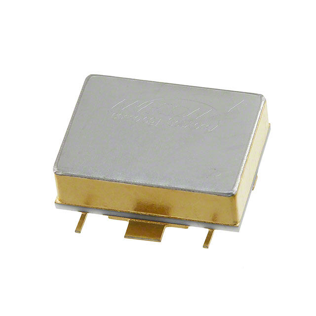
| 描述 | IC MIXER GAAS 3.0-3.8GHZ SOT-26 |
| 产品分类 | |
| 品牌 | Hittite Microwave Corporation |
| 数据手册 | |
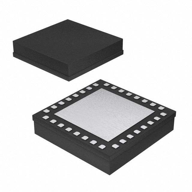
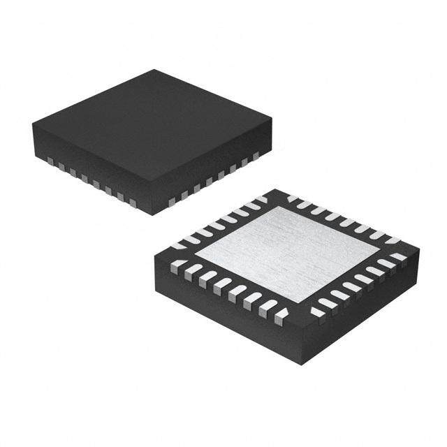
| 产品图片 |
|
| 产品型号 | HMC333E |
| RF类型 | WLL,WLAN |
| rohs | 无铅 / 符合限制有害物质指令(RoHS)规范要求 |
| 产品系列 | - |
| 供应商器件封装 | 6-SOP |
| 其它名称 | 1127-1335 |
| 包装 | 剪带 |
| 噪声系数 | 8.5dB |
| 增益 | - |
| 封装/外壳 | 6-LSOP(0.063",1.60mm 宽) |
| 标准包装 | 50 |
| 混频器数 | 1 |
| 电压-电源 | 3 V ~ 5 V |
| 电流-电源 | 7mA |
| 辅助属性 | 升/降频器 |
| 频率 | 3GHz ~ 3.8GHz |


- 商务部:美国ITC正式对集成电路等产品启动337调查
- 曝三星4nm工艺存在良率问题 高通将骁龙8 Gen1或转产台积电
- 太阳诱电将投资9.5亿元在常州建新厂生产MLCC 预计2023年完工
- 英特尔发布欧洲新工厂建设计划 深化IDM 2.0 战略
- 台积电先进制程称霸业界 有大客户加持明年业绩稳了
- 达到5530亿美元!SIA预计今年全球半导体销售额将创下新高
- 英特尔拟将自动驾驶子公司Mobileye上市 估值或超500亿美元
- 三星加码芯片和SET,合并消费电子和移动部门,撤换高东真等 CEO
- 三星电子宣布重大人事变动 还合并消费电子和移动部门
- 海关总署:前11个月进口集成电路产品价值2.52万亿元 增长14.8%


PDF Datasheet 数据手册内容提取
HMC333 333E / v01.0705 GaAs MMIC MIXER w/ INTEGRATED LO AMPLIFIER, 3.0 - 3.8 GHz Typical Applications Features The HMC333 / HMC333E is ideal for: Integrated LO Amplifi er w/ Pdiss: < 25 mW • Wireless Local Loop Conversion Loss / Noise Figure: 8.5 dB Low LO Drive Level: 0 dBm E Input IP3: +10 dBm 9 Single Positive Supply: 3V to 5V T Functional Diagram General Description T M E The HMC333 & HMC333E are single balanced mixer S ICs with integrated LO amplifi ers. This converter IC - can operate as an upconverter or downconverter L betwLeen 3.0 GHz and 3.8 GHz. With the integrated A LO amplifi er, the mixer requires an LO drive level of B only 0 dBm, and requires only 7 mA from a single - L O positive +3V rail. The mixer has 8.5 dB of conver- G sion loss, an input P1dB of 0 dBm and an input third S order intercept point of +10 dBm at 3.5 GHz. - S S R E X I B M O Electrical Specifi cations, T = +25° C A IF = 100 MHz Parameter LO = 0 dBm & Vdd = +3V Units Min. Typ. Max. Frequency Range, RF & LO 3.0 - 3.8 GHz Frequency Range, IF DC - 1.0 GHz Conversion Loss 8.5 11 dB Noise Figure (SSB) 8.5 11 dB LO to RF Isolation 10 15 dB LO to IF Isolation 5 10 dB RF to IF Isolation 10 15 dB IP3 (Input) 3 10 dBm 1 dB Compression (Input) -3 +1 dBm Supply Current (Idd) 7 mA * Unless otherwise noted, all measurements performed as downconverter, IF= 100 MHz. Information furnisheFd obry Apnrailcoge D, edviceelsi vise breylie,v eadn tdo bteo a cpcluaractee a nod rrdelieabrlse., Hpowleevaers, eno coFnotra pcritc eH, idtteiltieve rMy, iacnrdo wtoa pvlaec eC oorrdperosr: aAtnioalnog: Devices, Inc., responsibility is assumed by Analog Devices for its use, nor for any infringements of patents or other One Technology Way, P.O. Box 9106, Norwood, MA 02062-9106 9 - 194 rights of third parties tha2t 0ma yA relpsuhlt faro mR itos uasde. ,S pCechifiecaltmionss fsoubrjedct, toM chAan g0e1 w8ith2ou4t nPotihceo. Nnoe : P9h7o8n-e2: 75801--332394-437 0 0F (cid:127)a Ox:r d9e7r o8n-l2in5e 0at- w33w7w3.analog.com license is granted by implication or otherwise under any patent or patent rights of Analog Devices. Trademarks and registered trademarks are the property of their resOpercdtivee orw Onerns.-line at www.hAiptptilticea.tcioonm Support: Phone: 1-800-ANALOG-D
HMC333 / 333E v01.0705 GaAs MMIC MIXER w/ INTEGRATED LO AMPLIFIER, 3.0 - 3.8 GHz Conversion Gain vs. Temperature @ LO = 0 dBm Isolation @ LO = 0 dBm 0 0 dB) -5 -5 RLOF//IRFF N GAIN (-10 ON (dB)-10 ELO/IF SIO ATI 9 R L E O V S ON-15 +-4205 CC I-15 T C +85 C T -20 -20 2.4 2.8 3.2 3.6 4 4.4 2.4 2.E8 3.2 3.6 4 4.4 M FREQUENCY (GHz) FREQUENCY (GHz) S - L L Conversion Gain vs. LO Drive Return Loss @ LO = 0 dBm A B 0 0 - L O -5 G -6 dBm 0 dBm N (dB) -5 --42 ddBBmm ++24 ddBBmm dB)-10 S GAI SS ( - ONVERSION --1150 S RETURN LO--2105 LROF ERS C -25 X B I M -20 -30 2.4 2.8 3.2 3.6 4 4.4 0 1 2 3 4 5 6 FREQUENCY (GHz) FREQUENCY (GHz) O Conversion Gain vs. Vdd @ LO = 0 dBm IF Bandwidth @ LO = 0 dBm 0 0 B) -5 -5 d N ( B) N GAI-10 SE (d-10 O N CONVERSI-15 +++233...703VVV RESPO-15 CROETNUVRENR SLIOOSNS GAIN -20 -20 2.4 2.8 3.2 3.6 4 4.4 0 0.2 0.4 0.6 0.8 1 FREQUENCY (GHz) FREQUENCY (GHz) Information furnisheFd obry Apnrailcoge D, edviceelsi vise breylie,v eadn tdo bteo a cpcluaractee a nod rrdelieabrlse., Hpowleevaers, eno coFnotra pcritc eH, idtteiltieve rMy, iacnrdo wtoa pvlaec eC oorrdperosr: aAtnioalnog: Devices, Inc., responsibility is assumed by Analog Devices for its use, nor for any infringements of patents or other One Technology Way, P.O. Box 9106, Norwood, MA 02062-9106 rights of third parties tha2t 0ma yA relpsuhlt faro mR itos uasde. ,S pCechifiecaltmionss fsoubrjedct, toM chAan g0e1 w8ith2ou4t nPotihceo. Nnoe : P9h7o8n-e2: 75801--332394-437 0 0F (cid:127)a Ox:r d9e7r o8n-l2in5e 0at- w33w7w3.analog.com 9 - 195 license is granted by implication or otherwise under any patent or patent rights of Analog Devices. Trademarks and registered trademarks are the property of their resOpercdtivee orw Onerns.-line at www.hAiptptilticea.tcioonm Support: Phone: 1-800-ANALOG-D
HMC333 / 333E v01.0705 GaAs MMIC MIXER w/ INTEGRATED LO AMPLIFIER, 3.0 - 3.8 GHz Upconverter Performance Input P1dB vs. Conversion Gain @ LO = 0 dBm Temperature @ LO = 0 dBm 0 10 6 B) -5 AIN (d dBm) 2 E N G-10 dB ( O 1 9 ONVERSI-15 INPUT P -2 T +-4205 CC C -6 +85 C T -20 -10 M 3 3.2 3.4 3.6 3.8 4 2.9 3.1E 3.3 3.5 3.7 3.9 S FREQUENCY (GHz) FREQUENCY (GHz) - L InpLut IP3 vs. A Input IP3 vs. LO Drive* Temperature @ LO = 0 dBm* B 20 20 - L O G S 15 15 - m) m) S 3 (dB 10 S 3 (dB 10 R P P I I E 5 - 02 ddBBmm 5 +-4205 CC X +2 dBm +85 C I B M 0 0 3 3.2 3.4 3.6 3.8 4 3 3.2 3.4 3.6 3.8 4 FREQUENCY (GHz) FREQUENCY (GHz) O Input IP3 vs. Vdd @ LO = 0 dBm* Input P1dB vs. Vdd @ LO = 0 dBm 20 10 6 15 m) B P3 (dBm) 10 T P1dB (d -22 I U P +2.7V N +2.7V 5 +3.0V I +3.0V +3.3V -6 +3.3V 0 -10 3 3.2 3.4 3.6 3.8 4 2.9 3.1 3.3 3.5 3.7 3.9 FREQUENCY (GHz) FREQUENCY (GHz) * Two-tone input power= -10 dBm each tone, 1 MHz spacing. Information furnisheFd obry Apnrailcoge D, edviceelsi vise breylie,v eadn tdo bteo a cpcluaractee a nod rrdelieabrlse., Hpowleevaers, eno coFnotra pcritc eH, idtteiltieve rMy, iacnrdo wtoa pvlaec eC oorrdperosr: aAtnioalnog: Devices, Inc., responsibility is assumed by Analog Devices for its use, nor for any infringements of patents or other One Technology Way, P.O. Box 9106, Norwood, MA 02062-9106 9 - 196 rights of third parties tha2t 0ma yA relpsuhlt faro mR itos uasde. ,S pCechifiecaltmionss fsoubrjedct, toM chAan g0e1 w8ith2ou4t nPotihceo. Nnoe : P9h7o8n-e2: 75801--332394-437 0 0F (cid:127)a Ox:r d9e7r o8n-l2in5e 0at- w33w7w3.analog.com license is granted by implication or otherwise under any patent or patent rights of Analog Devices. Trademarks and registered trademarks are the property of their resOpercdtivee orw Onerns.-line at www.hAiptptilticea.tcioonm Support: Phone: 1-800-ANALOG-D
HMC333 / 333E v01.0705 GaAs MMIC MIXER w/ INTEGRATED LO AMPLIFIER, 3.0 - 3.8 GHz MxN Spurious @ IF Port Harmonics of LO nLO nLO Spur @ RF Port mRF 0 1 2 3 4 LO Freq. (GHz) 1 2 3 4 3 12 8 16 49 0 xx -9 -5 12 34 1 8 0 32 25 34 3.17 13 8 E20 39 2 33 49 40 40 43 3.34 17 10 22 42 3 68 56 68 48 72 3.51 15 14 26 48 9 4 77 80 79 80 71 3.68 14 17 25 42 T RF = 3.5 GHz @ -10 dBm 3.85 14 18 22 43 LO = 3.4 GHz @ 0 dBm All values in dBc below IF power level. LO = 0 dBm All values in dBc below input LO level @ RF port. T E M S - L L A B - L O G S - S S R E X B I M O Information furnisheFd obry Apnrailcoge D, edviceelsi vise breylie,v eadn tdo bteo a cpcluaractee a nod rrdelieabrlse., Hpowleevaers, eno coFnotra pcritc eH, idtteiltieve rMy, iacnrdo wtoa pvlaec eC oorrdperosr: aAtnioalnog: Devices, Inc., responsibility is assumed by Analog Devices for its use, nor for any infringements of patents or other One Technology Way, P.O. Box 9106, Norwood, MA 02062-9106 rights of third parties tha2t 0ma yA relpsuhlt faro mR itos uasde. ,S pCechifiecaltmionss fsoubrjedct, toM chAan g0e1 w8ith2ou4t nPotihceo. Nnoe : P9h7o8n-e2: 75801--332394-437 0 0F (cid:127)a Ox:r d9e7r o8n-l2in5e 0at- w33w7w3.analog.com 9 - 197 license is granted by implication or otherwise under any patent or patent rights of Analog Devices. Trademarks and registered trademarks are the property of their resOpercdtivee orw Onerns.-line at www.hAiptptilticea.tcioonm Support: Phone: 1-800-ANALOG-D
HMC333 / 333E v01.0705 GaAs MMIC MIXER w/ INTEGRATED LO AMPLIFIER, 3.0 - 3.8 GHz Absolute Maximum Ratings RF / IF Input (Vdd = +3V) +13 dBm LO Drive (Vdd = +3V) +13 dBm Vdd 5.5V Continuous Pdiss (Ta = 85 °C) E 238 mW (derate 2.64 mW/°C above 85 °C) 9 IF DC Current ±3 mA Storage Temperature -65 to +150 °C T Operating Temperature -40 to +85 °C T ELECTROSTATIC SENSITIVE DEVICE M E OBSERVE HANDLING PRECAUTIONS S - L L A Outline Drawing B - L O G S - S S R E X I B M O NOTES: 1. LEADFRAME MATERIAL: COPPER ALLOY 2. DIMENSIONS ARE IN INCHES [MILLIMETERS] 3. DIMENSION DOES NOT INCLUDE MOLDFLASH OF 0.15mm PER SIDE. 4. DIMENSION DOES NOT INCLUDE MOLDFLASH OF 0.25mm PER SIDE. 5. ALL GROUND LEADS MUST BE SOLDERED TO PCB RF GROUND. Package Information Part Number Package Body Material Lead Finish MSL Rating Package Marking [3] HMC333 Low Stress Injection Molded Plastic Sn/Pb Solder MSL1 [1] H333 XXXX HMC333E RoHS-compliant Low Stress Injection Molded Plastic 100% matte Sn MSL1 [2] 333E XXXX [1] Max peak refl ow temperature of 235 °C [2] Max peak refl ow temperature of 260 °C [3] 4-Digit lot number XXXX Information furnisheFd obry Apnrailcoge D, edviceelsi vise breylie,v eadn tdo bteo a cpcluaractee a nod rrdelieabrlse., Hpowleevaers, eno coFnotra pcritc eH, idtteiltieve rMy, iacnrdo wtoa pvlaec eC oorrdperosr: aAtnioalnog: Devices, Inc., responsibility is assumed by Analog Devices for its use, nor for any infringements of patents or other One Technology Way, P.O. Box 9106, Norwood, MA 02062-9106 9 - 198 rights of third parties tha2t 0ma yA relpsuhlt faro mR itos uasde. ,S pCechifiecaltmionss fsoubrjedct, toM chAan g0e1 w8ith2ou4t nPotihceo. Nnoe : P9h7o8n-e2: 75801--332394-437 0 0F (cid:127)a Ox:r d9e7r o8n-l2in5e 0at- w33w7w3.analog.com license is granted by implication or otherwise under any patent or patent rights of Analog Devices. Trademarks and registered trademarks are the property of their resOpercdtivee orw Onerns.-line at www.hAiptptilticea.tcioonm Support: Phone: 1-800-ANALOG-D
HMC333 / 333E v01.0705 GaAs MMIC MIXER w/ INTEGRATED LO AMPLIFIER, 3.0 - 3.8 GHz Pin Descriptions Pin Number Function Description Interface Schematic Power supply for the LO Amplifi er. Two external RF bypass 1 Vdd capacitors (10 pF & 10,000 pF) and an external inductor E (1.8 nH) are required. 9 T 2, 5 GND Ground: Pin must connect to RF ground. This pin is DC coupled. For applications not requiring opera- T tion to DC, this port should be DC blocked externally using a E M series capacitor whose value has been chosen to pass the 3 IF necessary IF frequency range. For operation to DC, this pin S must not source/sink more than 3mA of current or die non- function and possible die failure will result. - L L A This pin is AC coupled and matched to B 4 RF 50 Ohm from 3.0 - 3.8 GHz. - L O G S - This pin is AC coupled and matched to 6 LO S50 Ohm from 3.0 - 3.8 GHz S R E X B I M O Information furnisheFd obry Apnrailcoge D, edviceelsi vise breylie,v eadn tdo bteo a cpcluaractee a nod rrdelieabrlse., Hpowleevaers, eno coFnotra pcritc eH, idtteiltieve rMy, iacnrdo wtoa pvlaec eC oorrdperosr: aAtnioalnog: Devices, Inc., responsibility is assumed by Analog Devices for its use, nor for any infringements of patents or other One Technology Way, P.O. Box 9106, Norwood, MA 02062-9106 rights of third parties tha2t 0ma yA relpsuhlt faro mR itos uasde. ,S pCechifiecaltmionss fsoubrjedct, toM chAan g0e1 w8ith2ou4t nPotihceo. Nnoe : P9h7o8n-e2: 75801--332394-437 0 0F (cid:127)a Ox:r d9e7r o8n-l2in5e 0at- w33w7w3.analog.com 9 - 199 license is granted by implication or otherwise under any patent or patent rights of Analog Devices. Trademarks and registered trademarks are the property of their resOpercdtivee orw Onerns.-line at www.hAiptptilticea.tcioonm Support: Phone: 1-800-ANALOG-D
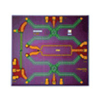
HMC333 / 333E v01.0705 GaAs MMIC MIXER w/ INTEGRATED LO AMPLIFIER, 3.0 - 3.8 GHz Application Circuit E 9 T T M E S - L L A B - L O G S - S S R E X I B M O Information furnisheFd obry Apnrailcoge D, edviceelsi vise breylie,v eadn tdo bteo a cpcluaractee a nod rrdelieabrlse., Hpowleevaers, eno coFnotra pcritc eH, idtteiltieve rMy, iacnrdo wtoa pvlaec eC oorrdperosr: aAtnioalnog: Devices, Inc., responsibility is assumed by Analog Devices for its use, nor for any infringements of patents or other One Technology Way, P.O. Box 9106, Norwood, MA 02062-9106 9 - 200 rights of third parties tha2t 0ma yA relpsuhlt faro mR itos uasde. ,S pCechifiecaltmionss fsoubrjedct, toM chAan g0e1 w8ith2ou4t nPotihceo. Nnoe : P9h7o8n-e2: 75801--332394-437 0 0F (cid:127)a Ox:r d9e7r o8n-l2in5e 0at- w33w7w3.analog.com license is granted by implication or otherwise under any patent or patent rights of Analog Devices. Trademarks and registered trademarks are the property of their resOpercdtivee orw Onerns.-line at www.hAiptptilticea.tcioonm Support: Phone: 1-800-ANALOG-D
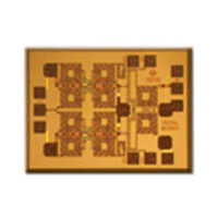
HMC333 / 333E v01.0705 GaAs MMIC MIXER w/ INTEGRATED LO AMPLIFIER, 3.0 - 3.8 GHz Evaluation PCB E 9 T T E M S - L L A B - L O G S - S S R E X B I M O List of Materials for Evaluation PCB 105128 [1] The circuit board used in the fi nal application should Item Description use RF circuit design techniques. Signal lines should J1 - J4 PCB Mount SMA RF Connector have 50 ohm impedance while the package ground C1 10 pF Capacitor, 0603 Pkg. leads should be connected directly to the ground C2 .01 μF Capacitor, 0603 Pkg. plane similar to that shown. A sufficient number of L1 1.8 nH Inductor, 0805 Pkg. via holes should be used to connect the top and U1 HMC333 / HMC333E Mixer bottom ground planes. The evaluation circuit board PCB [2] 103927 Evaluation Board shown is available from Hittite upon request. [1] Reference this number when ordering complete evaluation PCB [2] Circuit Board Material: Rogers 4350 Information furnisheFd obry Apnrailcoge D, edviceelsi vise breylie,v eadn tdo bteo a cpcluaractee a nod rrdelieabrlse., Hpowleevaers, eno coFnotra pcritc eH, idtteiltieve rMy, iacnrdo wtoa pvlaec eC oorrdperosr: aAtnioalnog: Devices, Inc., responsibility is assumed by Analog Devices for its use, nor for any infringements of patents or other One Technology Way, P.O. Box 9106, Norwood, MA 02062-9106 rights of third parties tha2t 0ma yA relpsuhlt faro mR itos uasde. ,S pCechifiecaltmionss fsoubrjedct, toM chAan g0e1 w8ith2ou4t nPotihceo. Nnoe : P9h7o8n-e2: 75801--332394-437 0 0F (cid:127)a Ox:r d9e7r o8n-l2in5e 0at- w33w7w3.analog.com 9 - 201 license is granted by implication or otherwise under any patent or patent rights of Analog Devices. Trademarks and registered trademarks are the property of their resOpercdtivee orw Onerns.-line at www.hAiptptilticea.tcioonm Support: Phone: 1-800-ANALOG-D