ICGOO在线商城 > 射频/IF 和 RFID > RF 混频器 > ADL5801ACPZ-R7
 Datasheet下载
- 型号: ADL5801ACPZ-R7
- 制造商: Analog
- 库位|库存: xxxx|xxxx
- 要求:
| 数量阶梯 | 香港交货 | 国内含税 |
| +xxxx | $xxxx | ¥xxxx |
查看当月历史价格
查看今年历史价格
ADL5801ACPZ-R7产品简介:
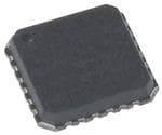
ICGOO电子元器件商城为您提供ADL5801ACPZ-R7由Analog设计生产,在icgoo商城现货销售,并且可以通过原厂、代理商等渠道进行代购。 ADL5801ACPZ-R7价格参考¥44.04-¥61.49。AnalogADL5801ACPZ-R7封装/规格:RF 混频器, RF Mixer IC Cellular Up/Down Converter 10MHz ~ 6GHz 24-LFCSP-VQ (4x4)。您可以下载ADL5801ACPZ-R7参考资料、Datasheet数据手册功能说明书,资料中有ADL5801ACPZ-R7 详细功能的应用电路图电压和使用方法及教程。
ADL5801ACPZ-R7是Analog Devices Inc.推出的一款高性能、有源混频器,属于RF混频器类别。该器件广泛应用于需要高频信号处理的通信系统中。其典型应用场景包括无线基础设施设备,如蜂窝基站的接收和中频采样架构,适用于GSM、CDMA、WCDMA、LTE等多种通信标准。

ADL5801ACPZ-R7具备宽频带射频(RF)和本振(LO)输入范围,支持从30 MHz至6 GHz的RF信号处理,使其非常适合多频段、多模式无线电设计。因此,它常用于软件定义无线电(SDR)、点对点微波通信、卫星通信系统以及军事和宽带通信设备中。

此外,该混频器具有高线性度和低噪声系数,有助于提升接收链路的动态范围和灵敏度,适用于高性能接收机前端设计。其集成的LO缓冲放大器降低了对外部驱动的需求,简化了系统设计。封装采用紧凑的3 mm × 3 mm LFCSP,适合高密度PCB布局,广泛用于便携式和空间受限的射频模块。

总之,ADL5801ACPZ-R7凭借其宽带性能、高集成度和优异的射频特性,主要应用于现代无线通信系统中的上变频和下变频环节,尤其适用于要求高动态性能和多频段兼容性的高端射频设计。
| 参数 | 数值 |
| 产品目录 | |
| 描述 | IC MXR 10MHZ-6GHZ UP/DWN 24LFCSP |
| 产品分类 | |
| 品牌 | Analog Devices Inc |
| 数据手册 | |
| 产品图片 |
|
| 产品型号 | ADL5801ACPZ-R7 |
| PCN组件/产地 | |
| RF类型 | 手机 |
| rohs | 无铅 / 符合限制有害物质指令(RoHS)规范要求 |
| 产品系列 | - |
| 供应商器件封装 | 24-LFCSP-VQ(4x4) |
| 其它名称 | ADL5801ACPZ-R7DKR |
| 包装 | Digi-Reel® |
| 噪声系数 | 9.75dB |
| 增益 | 1.8dB |
| 封装/外壳 | 24-VFQFN 裸露焊盘,CSP |
| 标准包装 | 1 |
| 混频器数 | 1 |
| 电压-电源 | 4.75 V ~ 5.25 V |
| 电流-电源 | 130mA |
| 视频文件 | http://www.digikey.cn/classic/video.aspx?PlayerID=1364138032001&width=640&height=505&videoID=2245193150001 |
| 辅助属性 | 升/降频器 |
| 频率 | 10MHz ~ 6GHz |


- 商务部:美国ITC正式对集成电路等产品启动337调查
- 曝三星4nm工艺存在良率问题 高通将骁龙8 Gen1或转产台积电
- 太阳诱电将投资9.5亿元在常州建新厂生产MLCC 预计2023年完工
- 英特尔发布欧洲新工厂建设计划 深化IDM 2.0 战略
- 台积电先进制程称霸业界 有大客户加持明年业绩稳了
- 达到5530亿美元!SIA预计今年全球半导体销售额将创下新高
- 英特尔拟将自动驾驶子公司Mobileye上市 估值或超500亿美元
- 三星加码芯片和SET,合并消费电子和移动部门,撤换高东真等 CEO
- 三星电子宣布重大人事变动 还合并消费电子和移动部门
- 海关总署:前11个月进口集成电路产品价值2.52万亿元 增长14.8%


PDF Datasheet 数据手册内容提取
High IP3, 10 MHz to 6 GHz, Active Mixer Data Sheet ADL5801 FEATURES FUNCTIONAL BLOCK DIAGRAM Broadband upconverter/downconverter VPLO GND NC IFONIFOPGND 24 23 22 21 20 19 Power conversion gain of 1.8 dB Broadband RF, LO, and IF ports SSB noise figure (NF) of 9.75 dB GND 1 ADL5801 18 VPRF Input IP3: 28.5 dBm GND 2 17 GND Input P1dB: 13.3 dBm LOIP 3 16 RFIP Typical LO drive: 0 dBm V2I Single-supply operation: 5 V at 130 mA LOIN 4 15 RFIN Adjustable bias for low power operation GND 5 14 GND Exposed paddle, 4 mm × 4 mm, 24-lead LFCSP package GND 6 13 VPDT BIAS DET APPLICATIONS RCealdluiola lrin bka dseo wstnactioonnv reercteerivse rs VP7LOGN8DEN9BLVS1E0TDE11TOG1N2D 08079-001 Broadband block conversion Figure 1. Instrumentation GENERAL DESCRIPTION The ADL5801 uses a high linearity, doubly balanced, active The balanced active mixer arrangement provides superb LO-to- mixer core with integrated LO buffer amplifier to provide high RF and LO-to-IF leakage, typically better than −40 dBm. The IF dynamic range frequency conversion from 10 MHz to 6 GHz. outputs are designed to provide a typical voltage conversion The mixer benefits from a proprietary linearization architecture gain of 7.8 dB when loaded into a 200 Ω load. The broad that provides enhanced input IP3 performance when subject to frequency range of the open-collector IF outputs allows the high input levels. A bias adjust feature allows the input linearity, ADL5801 to be applied as an upconverter for various transmit SSB noise figure, and dc current to be optimized using a single applications. control pin. An optional input power detector is provided for The ADL5801 is fabricated using a SiGe high performance IC adaptive bias control. The high input linearity allows the device process. The device is available in a compact 4 mm × 4 mm, to be used in demanding cellular applications where in-band 24-lead LFCSP package and operates over a −40°C to +85°C blocking signals may otherwise result in degradation in dynamic temperature range. An evaluation board is also available. performance. The adaptive bias feature allows the part to provide high input IP3 performance when presented with large blocking signals. When blockers are removed, the ADL5801 can auto- matically bias down to provide low noise figure and low power consumption. Rev. E Document Feedback Information furnished by Analog Devices is believed to be accurate and reliable. However, no responsibility is assumed by Analog Devices for its use, nor for any infringements of patents or other One Technology Way, P.O. Box 9106, Norwood, MA 02062-9106, U.S.A. rliicgehntsse o ifs t hgirradn pteadrt bieys itmhaptl imcaatyio rne sourl to ftrhoemrw itiss ue suen. Sdpeer cainficya ptiaotnesn st uobr jpecatt eton tc hriagnhgtse owf iAthnoaulot gn oDteicvei.c Neso. Tel: 781.329.4700 ©2010–2014 Analog Devices, Inc. All rights reserved. Trademarks and registered trademarks are the property of thei r respective owners. Technical Support www.analog.com
ADL5801 Data Sheet TABLE OF CONTENTS Features .............................................................................................. 1 Circuit Description......................................................................... 27 Applications ....................................................................................... 1 LO Amplifier and Splitter.......................................................... 27 Functional Block Diagram .............................................................. 1 RF Voltage-to-Current (V-to-I) Converter ............................. 27 General Description ......................................................................... 1 Mixer Core .................................................................................. 27 Revision History ............................................................................... 2 Mixer Output Load .................................................................... 27 Specifications ..................................................................................... 3 RF Detector ................................................................................. 28 Absolute Maximum Ratings ............................................................ 6 Bias Circuit .................................................................................. 28 ESD Caution .................................................................................. 6 Applications Information .............................................................. 31 Pin Configuration and Function Descriptions ............................. 7 Basic Connections ...................................................................... 31 Typical Performance Characteristics ............................................. 8 RF and LO Ports ......................................................................... 31 Downconverter Mode with a Broadband Balun ...................... 8 IF Port .......................................................................................... 32 Downconverter Mode with a Mini-Circuits® TC1-1-43M+ Downconverting to Low Frequencies ...................................... 33 Input Balun .................................................................................. 12 Broadband Operation ................................................................ 34 Downconverter Mode with a Johanson 3.5 GHz Single-Ended Drive of RF and LO Inputs ............................... 36 Input Balun .................................................................................. 14 Evaluation Board ............................................................................ 38 Downconverter Mode with a Johanson 5.7 GHz Input Balun .................................................................................. 16 Outline Dimensions ....................................................................... 40 Upconverter Mode with a 900 MHz Output Match .............. 18 Ordering Guide .......................................................................... 40 Upconverter Mode with a 2.1 GHz Output Match ................ 20 Spur Performance ....................................................................... 23 REVISION HISTORY 4/14—Rev. D to Rev. E Added Downconverting to Low Frequencies Section and Figure 97; Renumbered Sequentially ........................................... 32 Changes to Figure 1 .......................................................................... 1 Added Broadband Operation Section and Figure 98 to Changes to Table 1 ............................................................................ 4 Figure 101 ........................................................................................ 33 Changes to Figure 87 and Deleted Table 4; Renumbered Added Single-Ended Drive of RF and LO Inputs Section and Sequentially ..................................................................................... 27 Figure 102 to Figure 105 ................................................................ 35 Changes to RF Detector Section and Bias Circuit Section; Updated Outline Dimensions ....................................................... 39 Added Table 4 and Table 5; Renumbered Sequentially, and Added Figure 92, Figure 93, Figure 94, and Figure 95; 7/11—Rev. 0 to Rev. A Renumbered Sequentially .............................................................. 29 Changes to Specifications Section ................................................... 3 3/14—Rev. C to Rev. D Changes to Typical Performance Characteristics Section ........... 8 Changes to Spur Performance Section ........................................ 23 Changes to Pin 9, Table 3 ................................................................. 7 Changes to RF Voltage-to-Current (V-to-I) Converter 8/13—Rev. B to Rev. C Section .............................................................................................. 27 Changes to Table 8 .......................................................................... 38 Changes to RF Detector Section ................................................... 28 Changes to RF and LO Ports Section ........................................... 30 7/13—Rev. A to Rev. B 2/10—Revision 0: Initial Version Added Disable Voltage and Enable Voltage; Table 1 .................... 3 Changes to Table 5 and Figure 96 ................................................. 31 Rev. E | Page 2 of 40
Data Sheet ADL5801 SPECIFICATIONS V = 5 V, T = 25°C, f = 900 MHz, f = (f − 153 MHz), LO power = 0 dBm, Z 1 = 50 Ω, VSET = 3.6 V, unless otherwise noted. S A RF LO RF 0 Table 1. Parameter Test Conditions Min Typ Max Unit RF INPUT INTERFACE Return Loss Tunable to >20 dB over a limited bandwidth 12 dB Input Impedance 50 Ω RF Frequency Range 10 6000 MHz OUTPUT INTERFACE Output Impedance Differential impedance, f = 200 MHz 230 Ω IF Frequency Range Can be matched externally to 3000 MHz LF 600 MHz DC Bias Voltage2 Externally generated 4.75 V 5.25 V S LO INTERFACE LO Power −10 0 +10 dBm Return Loss 15 dB Input Impedance 50 Ω LO Frequency Range 10 6000 MHz POWER INTERFACE Supply Voltage 4.75 5 5.25 V Quiescent Current Resistor programmable 130 200 mA Disable Current ENBL pin high to disable the device 50 mA Disable Voltage ENBL pin high to disable the device 2.5 5 V Enable Voltage ENBL pin low to enable the device 0 1.8 V Enable Time Time from ENBL pin low to enable 182 ns Disable Time Time from ENBL pin high to disable 28 ns DYNAMIC PERFORMANCE at f = 900 MHz/1900 MHz3 RF Power Conversion Gain4 f = 900 MHz 1.8 dB RF f = 1900 MHz 1.8 dB RF Voltage Conversion Gain5 f = 900 MHz 7.8 dB RF f = 1900 MHz 7.8 dB RF SSB Noise Figure f = 900 MHz, VSET = 2.0 V 9.75 dB CENT f = 1900 MHz, VSET = 2.0 V 11.5 dB CENT SSB Noise Figure Under Blocking6 f = 900 MHz 19.5 dB CENT f = 1900 MHz 20 dB CENT Input Third-Order Intercept7 f = 900 MHz 28.5 dBm CENT f = 1900 MHz 26.4 dBm CENT Input Second-Order Intercept8 f = 900 MHz 63 dBm CENT f = 1900 MHz 49.7 dBm CENT Input 1 dB Compression Point f = 900 MHz 13.3 dBm RF f = 1900 MHz 12.7 dBm RF LO-to-IF Output Leakage Unfiltered IF output −27 dBm LO-to-RF Input Leakage −30 dBm RF-to-IF Output Isolation −35 dBc IF/2 Spurious9 0 dBm input power, f = 900 MHz −67.5 dBc RF 0 dBm input power, f = 1900 MHz −53 dBc RF IF/3 Spurious9 0 dBm input power, f = 900 MHz −65.5 dBc RF 0 dBm input power, f = 1900 MHz −72.6 dBc RF Rev. E | Page 3 of 40
ADL5801 Data Sheet Parameter Test Conditions Min Typ Max Unit DYNAMIC PERFORMANCE at f = 2500 MHz10 RF Power Conversion Gain11 −6.1 dB Voltage Conversion Gain5 −0.1 dB SSB Noise Figure f = 2500 MHz, VSET = 2.0 V 10.6 dB CENT Input Third-Order Intercept12 f = 2500 MHz 25.5 dBm CENT Input Second-Order Intercept13 f = 2500 MHz 45.3 dBm CENT Input 1 dB Compression Point f = 2500 MHz 13.8 dBm CENT LO-to-IF Output Leakage Unfiltered IF output −31.5 dBm LO-to-RF Input Leakage −31.2 dBm RF-to-IF Output Isolation −42.5 dBc IF/2 Spurious9 0 dBm input power, f = 2600 MHz −50.6 dBc RF IF/3 Spurious9 0 dBm input power, f = 2600 MHz −59.8 dBc RF DYNAMIC PERFORMANCE at f = 3500 MHz14 RF Power Conversion Gain15 −6.44 dB Voltage Conversion Gain5 −0.44 dB SSB Noise Figure f = 3500 MHz, VSET = 3.6 V 15.8 dB CENT Input Third-Order Intercept7 f = 3500 MHz, VSET = 3.6 V 26.5 dBm CENT Input Second-Order Intercept8 f = 3500 MHz, VSET = 3.6 V 42.3 dBm CENT Input 1 dB Compression Point 12.5 dBm LO-to-IF Output Leakage Unfiltered IF output −30.2 dBm LO-to-RF Input Leakage −29.4 dBm RF-to-IF Output Isolation −29.7 dBc IF/2 Spurious9 0 dBm input power, f = 3800 MHz −47.1 dBc RF IF/3 Spurious9 0 dBm input power, f = 3800 MHz −57.8 dBc RF DYNAMIC PERFORMANCE at f = 5500 MHz16 RF Power Conversion Gain17 −5.2 dB Voltage Conversion Gain5 0.8 dB SSB Noise Figure f = 5500 MHz, VSET = 3.6 V 16.2 dB CENT Input Third-Order Intercept7 f = 5500 MHz, VSET = 3.6 V 22.7 dBm CENT Input Second-Order Intercept 8 f = 5500 MHz, VSET = 3.6 V 35.4 dBm CENT Input 1 dB Compression Point 11.3 dBm LO-to-IF Output Leakage Unfiltered IF output −42.6 dBm LO-to-RF Input Leakage −28.9 dBm RF-to-IF Output Isolation −46.7 dBc IF/2 Spurious9 0 dBm input power, f = 5800 MHz −44 dBc RF IF/3 Spurious9 0 dBm input power, f = 5800 MHz −47 dBc RF DYNAMIC PERFORMANCE at f = 900 MHz18 IF Power Conversion Gain19 −6 dB Voltage Conversion Gain5 0 dB SSB Noise Figure f = 900 MHz, f = 250 MHz, VSET = 2.0 V 10.6 dB IF RF Output Third-Order Intercept20 f = 153 MHz, VSET = 3.6 V 30.6 dBm CENT Output Second-Order Intercept 21 f = 153 MHz, VSET = 3.6 V 68.7 dBm CENT Output 1 dB Compression Point 11.1 dBm LO-to-IF Output Leakage Unfiltered IF output −33.8 dBm LO-to-RF Input Leakage −33.4 dBm IF/2 Spurious9 0 dBm input power, f = 140 MHz, −62.6 dBc RF f = 806 MHz IF IF/3 Spurious9 0 dBm input power, f = 140 MHz, −68.9 dBc RF f = 806 MHz IF Rev. E | Page 4 of 40
Data Sheet ADL5801 Parameter Test Conditions Min Typ Max Unit DYNAMIC PERFORMANCE at f = 2140 MHz22 IF Power Conversion Gain23 −7.25 dB Voltage Conversion Gain5 −1.25 dB SSB Noise Figure f = 2140 MHz, f = 190 MHz, VSET = 2.0 V 13.6 dB IF RF Output Third-Order Intercept24 f = 170 MHz, VSET = 3.6 V 24 dBm CENT Output Second-Order Intercept25 f = 170 MHz, VSET = 3.6 V 70 dBm CENT Output 1 dB Compression Point 9.9 dBm LO-to-IF Output Leakage Unfiltered IF output −23.8 dBm LO-to-RF Input Leakage −33.2 dBm IF/2 Spurious9 0 dBm input power, f = 140 MHz, −51.5 dBc RF f = 2210 MHz IF 1 Z0 is the characteristic impedance assumed for all measurements and the PCB. 2 Supply voltage must be applied from an external circuit through choke inductors 3 VS = 5 V, TA = 25°C, fRF = 900 MHz/1900 MHz, fLO = (fRF – 153 MHz), LO power = 0 dBm, Z01= 50 Ω, VSET = 3.8 V, unless otherwise noted. 4 Excluding 4:1 IF port transformer (TC4-1W+), RF and LO port transformers (TC1-1-13M+), and PCB loss. 5 ZSOURCE = 50 Ω, differential; ZLOAD = 200 Ω differential; ZSOURCE is the impedance of the source instrument; ZLOAD is the load impedance at the output. 6 fRF = fCENT, fBLOCKER = (fCENT − 5) MHz, fLO = (fCENT − 153) MHz, blocker level = 0 dBm. 7 fRF1 = (fCENT − 1) MHz, fRF2 = (fCENT) MHz, fLO = (fCENT – 153) MHz, each RF tone at −10 dBm. 8 fRF1 = (fCENT ) MHz, fRF2 = (fCENT + 100) MHz, fLO = (fCENT – 153) MHz, each RF tone at −10 dBm. 9 For details, see the Spur Performance section. 10 VS = 5 V, TA = 25°C, fRF = 2500 MHz, fLO = (fRF – 211 MHz), LO power = 0 dBm, Z01 = 50 Ω, VSET = 3.8 V, unless otherwise noted. 11 Including 4:1 IF port transformer (TC4-1W+), RF and LO port transformers (TC1-1-43M+ and TC1-1-13M+ respectively), and PCB loss. 12 fRF1 = (fCENT − 1) MHz, fRF2 = (fCENT) MHz, fLO = (fCENT – 211) MHz, each RF tone at −10 dBm. 13 fRF1 = (fCENT ) MHz, fRF2 = (fCENT + 100) MHz, fLO = (fCENT – 211) MHz, each RF tone at −10 dBm 14 VS = 5 V, TA = 25°C, fRF = 3500 MHz, fLO = (fRF – 153 MHz), LO power = 0 dBm, Z01 = 50 Ω, VSET = 3.6 V, unless otherwise noted. 15 Including 4:1 IF port transformer (TC4-1W+), RF and LO port transformers (3600BL14M050), and PCB loss. 16 VS = 5 V, TA = 25°C, fRF = 5500 MHz, fLO = (fRF – 153 MHz), LO power = 0 dBm, Z01 = 50 Ω, VSET = 3.6 V, unless otherwise noted. 17 Including 4:1 IF port transformer (TC4-1W+), RF and LO port transformers (5400BL14B050), and PCB loss. 18 VS = 5 V, TA = 25°C, fRF = 153 MHz, fLO = (fRF + 900 MHz), LO power = 0 dBm, Z01 = 50 Ω, VSET = 3.6 V, unless otherwise noted. 19 Including 4:1 IF port transformer (TC4-14+), RF and LO transformers (TC1-1-13M+), and PCB loss. 20 fRF1 = (fCENT − 1) MHz, fRF2 = (fCENT) MHz, fLO = (fCENT + 900 MHz), each RF tone at −10 dBm. 21 fRF1 = (fCENT ) MHz, fRF2 = (fCENT + 100) MHz, fLO = (fCENT + 900) MHz, each RF tone at −10 dBm. 22 VS = 5 V, TA = 25°C, fRF = 153MHz, fLO = (fRF + 2140 MHz), LO power = 0 dBm, Z01 = 50 Ω, VSET = 4 V, unless otherwise noted. 23 Including 4:1 IF port transformer (1850BL15B200), RF and LO port transformers (TC1-1-13M+), and PCB loss. 24 fRF1 = (fCENT − 1) MHz, fRF2 = (fCENT) MHz, fLO = (fCENT + 2140 MHz), each RF tone at −10 dBm. 25 fRF1 = (fCENT ) MHz, fRF2 = (fCENT + 100) MHz, fLO = (fCENT + 2140) MHz, each RF tone at −10 dBm. Rev. E | Page 5 of 40
ADL5801 Data Sheet ABSOLUTE MAXIMUM RATINGS Stresses above those listed under Absolute Maximum Ratings may cause permanent damage to the device. This is a stress Table 2. rating only; functional operation of the device at these or any Parameter Rating other conditions above those indicated in the operational Supply Voltage, VPOS 5.5 V section of this specification is not implied. Exposure to absolute VSET, ENBL 5.5 V maximum rating conditions for extended periods may affect IFOP, IFON 5.5 V device reliability. RFIN Power 20 dBm ESD CAUTION Internal Power Dissipation 1.2 W θ (Exposed Paddle Soldered Down)1 26.5°C/W JA θ (at Exposed Paddle) 8.7°C/W JC Maximum Junction Temperature 150°C Operating Temperature Range −40°C to +85°C Storage Temperature Range −65°C to +150°C 1 As measured on the evaluation board. For details, see the Evaluation Board section. Rev. E | Page 6 of 40
Data Sheet ADL5801 PIN CONFIGURATION AND FUNCTION DESCRIPTIONS LPVODNGCNNOFIPOFIDNG 432109 222221 PIN 1 GND 1 INDICATOR 18VPRF GND 2 17GND LOIP 3 ADL5801 16RFIP LOIN 4 TOP VIEW 15RFIN GND 5 (Not to Scale) 14GND GND 6 13VPDT 789011121 ODLTOD LNBETN PGNSEG V EVD NOTES 1. THERE ISAN EXPOSEDPADDLE THAT 2 . NMCU S=T N BOE C SOONLNDEECRTE.DTO GROUND. 08079-002 Figure 2. Pin Configuration Table 3. Pin Function Descriptions Pin No. Mnemonic Description 1, 2, 5, 6, 8, 12, GND Device Common (DC Ground). 14, 17, 19, 23 3, 4 LOIP, LOIN Differential LO Input Terminal. Internally matched to 50 Ω. Must be ac-coupled. 7, 24 VPLO Positive Supply Voltage for LO System. 9 ENBL Detector and Mixer Bias Enable. Pull the pin high to disable the internal detector and mixer bias circuit. The device can be operated in this mode by setting the bias level using an external supply or connecting a resistor from the VSET pin to the positive supply. See the Circuit Description section for more details. Pull the pin low to enable the internal detector and mixer bias circuit. 10 VSET Input IP3 Bias Adjustment. The voltage presented to the VSET pin sets the internal bias of the mixer core and allows for adaptive control of the input IP3 and NF characteristics of the mixer core. 11 DETO Detector Output. The DETO pin should be loaded with a capacitor to ground. The developed voltage is proportional to the rms input level. When the DETO output voltage is connected to the VSET input pin, the part auto biases and increases input IP3 performance when presented with large signal input levels. 13 VPDT Positive Supply Voltage for Detector. 15, 16 RFIN, RFIP Differential RF Input Terminal. Internally matched to 50 Ω differential input impedance. Must be ac-coupled. 18 VPRF Positive Supply Voltage for RF Input System. 20, 21 IFOP, IFON Differential IF Output Terminal. Bias must be applied through pull-up choke inductors or the center tap of the IF transformer. 22 NC Not Connected. EPAD The exposed paddle must be soldered to ground. Rev. E | Page 7 of 40
ADL5801 Data Sheet TYPICAL PERFORMANCE CHARACTERISTICS DOWNCONVERTER MODE WITH A BROADBAND BALUN V = 5 V, T = 25°C, VSET = 3.8 V, IF = 153 MHz, as measured using a typical circuit schematic with low-side local oscillator (LO), unless S A otherwise noted. Insertion loss of input and output baluns (TC1-1-13M+, TC4-1W+) is extracted from the gain measurement. 6 6 35 5 5 30 4 TA = –40°C 3 TA = +25°C 4 25 m) GAIN (dB) 012 TA = +85°C GAIN (dB) 3 GGIINNAAPPIIUUNNTT == II PP91093300 ==M0 M91H09Hz00zM0MHHzz 20 PUT IP3 (dB N 2 15 I –1 –2 1 10 –3 –4 0 5 500 1000 RF1 F5R00EQUENCY20 (0M0Hz) 2500 3000 08079-003 –15 –10 –5 LO LEVE0L (dBm) 5 10 15 08079-006 Figure 3. Power Conversion Gain vs. RF Frequency Figure 6. Power Conversion Gain and Input IP3 vs. LO Power 4.0 100 90 3.5 MEAN = 1.87 80 SD = 0.03 3.0 70 %) AIN (dB) 22..05 900MHz QUENCY ( 6500 G E 40 1.5 R F 1900MHz 30 1.0 20 0.5 10 0 0 0 50 IF F1R00EQUENCY 1(5M0Hz) 200 250 08079-004 1.700 1.740 1.780POW1.820ER C1.860ONVE1.900RSION1.940 GAIN 1.980(dB) 2.020 2.060 2.10008079-007 Figure 4. Power Conversion Gain vs. IF Frequency Figure 7. Power Conversion Gain Distribution 3.0 0.18 3.0 GAIN = 900MHz 2.5 GIPAOSIN = = 9 10900M0HMzHz 0.16 2.5 TA = –40°C IPOS = 1900MHz 2.0 0.14 TA = +25°C A) 1.5 0.12 NT ( 2.0 N (dB) 1.0 0.10 URRE N (dB) 1.5 TA = +85°C GAI LY C GAI 0.5 0.08 P UP 1.0 S 0 0.06 0.5 –0.5 0.04 –1.0 0.02 0 2.0 2.5 3.0 VSE3T.5 (V) 4.0 4.5 5.0 08079-005 4.7 4.8 4.9 SUP5P.L0Y (V) 5.1 5.2 5.3 08079-008 Figure 5. Power Conversion Gain and Supply Current vs. VSET Figure 8. Power Conversion Gain vs. Supply Voltage Rev. E | Page 8 of 40
Data Sheet ADL5801 35 70 TA = –40°C 30 TA = +25°C 60 TA = –40°C 25 50 TA = +25°C m) m) TA = +85°C B B P3 (d 20 TA = +85°C P2 (d 40 UT I 15 UT I 30 P P N N I I 10 20 5 10 0 0 500 1000 RF1 F5R00EQUENCY20 (0M0Hz) 2500 3000 08079-009 500 1000 RF1 F50R0EQUENC2Y0 (0M0Hz) 2500 3000 08079-012 Figure 9. Input IP3 vs. RF Frequency Figure 12. Input IP2 vs. RF Frequency 40 80 70 35 900MHz 60 Bm)30 900MHz Bm) 50 d d 1900MHz P3 (25 1900MHz P2 ( 40 UT I UT I NP NP 30 I20 I 20 15 10 10 0 0 50 IF F1R00EQUENCY1 (5M0Hz) 200 250 08079-010 0 50 IF F1R00EQUENCY 1(5M0Hz) 200 250 08079-013 Figure 10. Input IP3 vs. IF Frequency Figure 13. Input IP2 vs. IF Frequency 30 20 80 70 25 18 900MHz 60 P3 (dBm) 1250 1146 GURE (dB) P2 (dBm) 4500 1900MHz UT I E FI UT I INP 10 12 NOIS INP 30 20 5 IINNPPUUTTIIPP33 == 910900M0MHHzz 10 10 NF = 900MHz NF = 1900MHz 0 8 0 2.0 2.5 3.0 VSE3.T5 (V) 4.0 4.5 5.0 08079-011 2.0 2.5 3.0 VSE3.T5 (V) 4.0 4.5 5.0 08079-014 Figure 11. Input IP3 and Noise Figure vs. VSET Figure 14. Input IP2 vs. VSET Rev. E | Page 9 of 40
ADL5801 Data Sheet 20 25 18 16 TA = +85°C TA = +25°C 20 B) 14 d m) E ( dB 12 UR 15 UT P1dB ( 108 TA = –40°C OISE FIG 10 1900MHz P N 900MHz N B I 6 S S 4 5 2 0 0 500 1000 RF1 F5R00EQUENCY2 0(0M0Hz) 2500 3000 08079-015 0 100 200IF FR3E0Q0UENC4Y0 0(MHz)500 600 700 08079-018 Figure 15. Input P1dB vs. RF Frequency Figure 18. SSB Noise Figure vs. IF Frequency (VSET = 2.0 V) 20 30 18 25 16 B) Bm) 14 900MHz RE (d 20 RF B=L 1O8C46KMEHRz =, I1F8 =41 1M5H3 zMHz d 12 1900MHz U 1dB ( 10 E FIG 15 P S T OI U 8 N NP B 10 I 6 SS RF = 951MHz, IF = 153 MHz BLOCKER = 946MHz 4 5 2 0 00 50 IF F1R00EQUENCY1 (5M0Hz) 200 250 08079-016 –30 –25 –20BLOC–K1E5R LEV–E1L0 (dBm)–5 0 5 08079-019 Figure 16. Input P1dB vs. IF Frequency Figure 19. SSB Noise Figure vs. Blocker Level (VSET = 2.0 V) 18 20 16 TA = +85°C 18 16 URE (dB)1124 TA = +25°C URE (dB) 1124 1900MHz G10 G OISE FI 8 TA = –40°C OISE FI 180 900MHz N N SSB 6 SSB 6 4 4 2 2 0500 1000 RF1 F50R0EQUENC2Y0 (0M0Hz) 2500 300008079-017 0–15 –10 –5 LO LEVE0L (dBm) 5 10 15 08079-020 Figure 17. SSB Noise Figure vs. RF Frequency (VSET = 2.0 V) Figure 20. SSB Noise Figure vs. LO Power (VSET = 2.0 V) Rev. E | Page 10 of 40
Data Sheet ADL5801 0 –10 –15 5 TA = –40°C –20 TA = +25°C B)10 Bm) –25 TA = +85°C d d OSS (15 AGE ( –30 L K N A –35 R E RETU20 O-IF L –40 RF 25 O-T –45 L –50 30 –55 35 –60 0 500 10R0F0 FREQ1U5E0N0CY (M2H0z0)0 2500 3000 08079-021 500 1000 LO1 F5R00EQUENCY20 (0M0Hz) 2500 3000 08079-024 Figure 21. RF Return Loss vs. RF Frequency Figure 24. LO-to-IF Leakage vs. LO Frequency 0 –10 –15 TA = –40°C 5 TA = +25°C m) –20 TA = +85°C dB)10 dB –25 S ( E ( S G –30 O15 A L K N A –35 ETUR20 RF LE –40 LO R25 O-TO- –45 L –50 30 –55 350 500 10L0O0 FREQ1U5E00NCY (M2H0z0)0 2500 3000 08079-022 –60500 1000 LO1 F50R0EQUENC2Y0 (0M0Hz) 2500 3000 08079-025 Figure 22. LO Return Loss vs. LO Frequency Figure 25. LO-to-RF Leakage vs. LO Frequency 500 4 0 c)–10 400 2 B d N ( ESISTANCE (Ω) 230000 0–2 PACITANCE (pF) AUTPUT ISOLTIO––3200 TA = +85°C R CA F O–40 100 –4 RF-TO-I–50 TA = –40°C TA = +25°C 0 –6 –60 10 IF F1R0E0QUENCY (MHz) 1000 3000 08079-023 500 1000 RF1 F5R00EQUENCY2 0(0M0Hz) 2500 3000 08079-026 Figure 23. IF Differential Output Impedance (R Parallel C Equivalent) Figure 26. RF-to-IF Leakage vs. RF Frequency Rev. E | Page 11 of 40
ADL5801 Data Sheet DOWNCONVERTER MODE WITH A MINI-CIRCUITS® TC1-1-43M+ INPUT BALUN V = 5 V, T = 25°C, VSET = 3.8 V, IF = 211 MHz, as measured using a typical circuit schematic with low-side local oscillator (LO), unless S A otherwise noted. Insertion loss of input and output baluns (TC1-1-43M+, TC4-1W+) is included in the gain measurement. 6 30 20 5 25 18 4 IIP32500MHz 3 m)20 16 dB) GAIN (dB) 12 UT IP3 (dB15 14 E FIGURE ( 0 P S IN10 12 NOI –1 NF2500MHz –2 5 10 –3 –42000 2100 2200 2300RF 2F4R0E0Q2U5E0N0CY2 6(0M0Hz2)700 2800 2900 3000 08079-027 02.0 2.5 3.0 VSE3T.5 (V) 4.0 4.5 5.08 08079-030 Figure 27. Power Conversion Gain vs. RF Frequency Figure 30. Input IP3 and Noise Figure vs. VSET 1.0 0.18 60 0.5 GAIN2500M 0.16 50 0.14 0 A) –0.5 0.12 NT ( Bm) 40 GAIN (dB)–1.0 IPOS2500M 00..0180 LY CURRE PUT IP2 (d 30 –1.5 P N 0.06 UP I 20 S –2.0 0.04 10 –2.5 0.02 –3.02.0 2.5 3.0 VSE3T.5 (V) 4.0 4.5 5.00 08079-028 20000 2100 2200 2300RF 2F4R0E0Q2U5E0N0CY2 6(0M0Hz2)700 2800 2900 3000 08079-031 Figure 28. Power Conversion Gain and IPOS vs. VSET Figure 31. Input IP2 vs. RF Frequency 30 80 29 70 28 60 27 NPUT IP3 (dBm) 222456 NPUT IP2 (dBm) 345000 I I 23 20 22 10 21 202000 2100 2200 2300RF 2F4R0E0Q2U5E0N0CY2 6(0M0Hz2)700 2800 2900 3000 08079-029 02.0 2.5 3.0 VSE3T.5 (V) 4.0 4.5 5.0 08079-032 Figure 29. Input IP3 vs. RF Frequency Figure 32. Input IP2 vs. VSET Rev. E | Page 12 of 40
Data Sheet ADL5801 20 –10 18 –15 16 –20 m) Bm)14 E (dB –25 d12 G –30 B ( KA NPUT P1d108 O RF LEA ––4305 I 6 T –45 O L 4 –50 2 –55 02000 2100 2200 2300RF 2F4R0E0Q2U5E0N0CY2 6(0M0Hz2)700 2800 2900 3000 08079-033 –620000 2100 2200 230L0O2 F4R00EQ2U5E0N0CY2 6(0M0Hz2)700 2800 2900 3000 08079-036 Figure 33. Input P1dB vs. RF Frequency Figure 36. LO to RF Leakage vs. LO Frequency 25 –20 +85°C VSET 3.6V +85°C VSET 2V 20 +–4205°°CC VVSSEETT 33..66VV +–4205°°CC VVSSEETT 22VV N (dBc) –30 GURE (dB) 15 T ISOLATIO ––5400 OISE FI 10 OUTPU N F –60 O I T 5 F R –70 02000 2100 2200 2300RF 2F4R0E0Q2U5E0N0CY2 6(0M0Hz2)700 2800 2900 3000 08079-034 –820000 2100 2200 2300RF 2F4R0E0Q2U5E0N0CY2 6(0M0Hz2)700 2800 2900 3000 08079-037 Figure 34. Noise Figure vs. RF Frequency Figure 37. RF to IF Output Isolation vs. RF Frequency –10 –15 –20 m) B –25 d E ( G –30 A K A –35 E L O IF –40 T O –45 L –50 –55 –620000 2100 2200 230L0O2 F4R00EQ2U5E0N0CY2 6(0M0Hz2)700 2800 2900 3000 08079-035 Figure 35. LO to IF Leakage vs. LO Frequency Rev. E | Page 13 of 40
ADL5801 Data Sheet DOWNCONVERTER MODE WITH A JOHANSON 3.5 GHZ INPUT BALUN V = 5 V, T = 25°C, VSET = 3.6 V, IF = 153 MHz, as measured using a typical circuit schematic with low-side local oscillator (LO), unless S A otherwise noted. Insertion loss of input and output baluns (3600BL14M050, TC4-1W+) is included in the gain measurement. 6 30 28 5 –40°C +25°C 25 4 +85°C 23 3 m) 20 dB) GAIN (dB) 12 UT IP3 (dB 15 18 E FIGURE ( 0 P S IN 10 NOI –1 IIP3,–40°C IIP3,+25°C 13 –2 IIP3,+85°C 5 NF,–40°C –3 NNFF,,++2855°°CC –43000 3100 3200 3300RF 3F4R0E0Q3U5E0N0CY3 6(0M0Hz3)700 3800 3900 4000 08079-038 02.0 2.5 3.0 VSE3T.5 (V) 4.0 4.5 5.08 08079-041 Figure 38. Power Conversion Gain vs. RF Frequency Figure 41. Input IP3 and Noise Figure vs. VSET 2 0.20 50 0.18 0 +85°C 45 +25°C 0.16 –40°C –2 0.14 A) T ( m) 40 N (dB) –4 00..1102 URREN P2 (dB 35 GAI ––86 GGAAIINN+–4205°°CC 00..0068 SUPPLY C INPUT I 30 GAIN+85°C 0.04 –10 IIPPOOSS+–4205°°CC 25 IPOS+85°C 0.02 –122.0 2.5 3.0 VSE3T.5 (V) 4.0 4.5 5.00 08079-039 203000 3100 3200 3300RF 3F4R0E0Q3U5E0N0CY3 6(0M0Hz3)700 3800 3900 4000 08079-042 Figure 39. Power Conversion Gain and IPOS vs. VSET Figure 42. Input IP2 vs. RF Frequency 30 80 +85°C –40°C 70 +25°C 25 +25°C –40°C +85°C 60 Bm) 20 Bm) 50 d d 3 ( 2 ( P 15 P 40 T I T I U U NP NP 30 I 10 I 20 5 10 03000 3100 F3i2g0u0re3 43000R. IFn 3Fp4Ru0E0t QIP3U35E0 vN0sC. YR3 6F(0M F0Hrez3)q7u0e0nc3y8 00 3900 4000 08079-040 02.0 2.5 Figu3r.e0 43. InVpSEu3T.t5 (IVP)2 vs. V4.S0ET 4.5 5.0 08079-043 Rev. E | Page 14 of 40
Data Sheet ADL5801 20 –10 +85°C 18 +85°C –15 +25°C +25°C –40°C 16 –40°C –20 m) Bm) 14 E (dB–25 d 12 G–30 B ( KA NPUT P1d 108 O RF LEA––4305 I 6 OT–45 L 4 –50 2 –55 03000 3100 3200 3300RF 3F4R0E0Q3U5E0N0CY3 6(0M0Hz3)700 3800 3900 4000 08079-044 –603000 3100 3200 330L0O3 F4R00EQ3U5E0N0CY3 6(0M0Hz3)700 3800 3900 4000 08079-047 Figure 44. Input P1dB vs. RF Frequency Figure 47. LO to RF Leakage vs. LO Frequency 25 –20 +85°C, 3.6V +25°C, 3.6V –40°C, 3.6V 20 dBc) –30 GURE (dB) 15 T ISOLATION ( ––5400 ++–428055°°°CCC SE FI 10 +85°C, 2.0V +25°C, 2.0V –40°C, 2.0V UTPU NOI F O –60 O I T 5 F R –70 03000 3100Fig32u0r0e 4353.0 N0RoF i3Fs4eR0 E0FiQg3Uu5Er0eN0 CvsY3. 6 (R0MF0H Fz3r)e7q00ue3n8c0y0 3900 4000 08079-045 –830000Fig3u10re0 4382. 0R0F t3o3 0IF0R OF 3uF4Rt0pE0uQt3U I5sE0oN0lCaYt3i 6o(0Mn0H vzs3).7 R0F0 F3re80q0ue3n9c0y0 4000 08079-048 –10 –15 +85°C –20 +25°C m) –40°C B –25 d E ( G –30 A K A –35 E L O IF –40 T O –45 L –50 –55 –60 3000 3100 3200 330L0O3 F4R00EQ3U5E0N0CY3 6(0M0Hz3)700 3800 3900 4000 08079-046 Figure 46. LO to IF Leakage vs. LO Frequency Rev. E | Page 15 of 40
ADL5801 Data Sheet DOWNCONVERTER MODE WITH A JOHANSON 5.7 GHZ INPUT BALUN V = 5 V, T = 25°C, VSET = 3.6 V, IF = 153 MHz, as measured using a typical circuit schematic with low-side local oscillator (LO), unless S A otherwise noted. Insertion loss of input and output baluns (5400BL14B050, TC4-1W+) is included in the gain measurement. 6 25 35 5 –40°C +25°C 30 4 +85°C 20 3 m) 25 B) 2 dB 15 B) GAIN (d 01 NPUT IP3 ( 10 20 FIGURE (d I 15 E –1 S IIP3,–40°C OI –2 5 IIIIPP33,,++2855°°CC 10 N NF,–40°C –3 NF,+25°C NF,+85°C –45000 5100 5200 5300RF5 F4R00EQ5U5E0N0CY56 (0M0Hz5)700 5800 5900 6000 08079-049 02.0 2.5 3.0 VSE3T.5 (V) 4.0 4.5 5.05 08079-052 Figure 49. Power Conversion Gain vs. RF Frequency Figure 52. Input IP3 and Noise Figure vs. VSET 2 0.20 70 0 0.18 65 +85°C –2 0.16 60 +25°C –40°C 0.14 A) 55 –4 T ( m) N (dB) –6 00..1102 URREN P2 (dB 4550 GAI –1–08 0.08 Y CUPPL INPUT I 40 GAIN–40°C 0.06 S 35 –12 GAIN+25°C GAIN+85°C 0.04 30 IPOS–40°C –14 IPOS+25°C 0.02 25 IPOS+85°C –162.0 Figu2r.5e 50. Pow3.0er ConVvSEe3T.r5s (iVo)n Gai4n.0 and IPO4S.5 vs VSET 5.00 08079-050 205000 5100 F5i2g0u0re5 53030R. IFn 5Fp4Ru0E0t QIP5U25E 0vN0sC. YR5 6F(0M F0Hrez5q)7u0e0nc5y8 00 5900 6000 08079-053 30 80 –40°C +25°C +85°C +85°C 70 +25°C 25 –40°C 60 INPUT IP3 (dBm) 112050 INPUT IP2 (dBm) 345000 20 5 10 05000 5100 F5i2g0u0re5 53010R. IFn 5Fp4Ru0E0t QIP5U35E 0vN0sC. YR5 6F(0M F0Hrez5q)7u0e0nc5y8 00 5900 6000 08079-051 02.0 2.5 Figu3r.e0 54. InVpSEu3T.t5 (IVP)2 vs. V4.S0ET 4.5 5.0 08079-054 Rev. E | Page 16 of 40
Data Sheet ADL5801 20 –10 +85°C +85°C 18 +25°C –15 +25°C –40°C –40°C 16 –20 m) Bm) 14 E (dB –25 d 12 G –30 B ( KA NPUT P1d 108 O RF LEA ––4305 I 6 TO –45 L 4 –50 2 –55 05000 5100 5200 5300RF 5F4R0E0Q5U5E0N0CY5 6(0M0Hz5)700 5800 5900 6000 08079-055 –650000 5100 5200 530L0O5 F4R00EQ5U5E0N0CY5 6(0M0Hz5)700 5800 5900 6000 08079-058 Figure 55. Input P1dB vs. RF Frequency Figure 58. LO to RF Leakage vs. LO Frequency 25 –20 +85°C, 3.6V +25°C, 3.6V –40°C, 3.6V +85°C 20 dBc)–30 +–4205°°CC N ( RE (dB) 15 OLATIO–40 FIGU +85°C, 2.0V +25°C, 2.0V –40°C, 2.0V UT IS–50 OISE 10 OUTP N F –60 O I T 5 F R–70 05000Fig51u0r0e 5562.0 N0oi5s3e0 F0RiFg 5uF4Rr0eE0 vQs5U.5 ER0NF0C FY5re 6(q0M0uHez5n)7c0y0, V5S8ET0 =0 35.960 V0 6000 08079-056 –805000Fig5u10r0e 5592.0 R0F t5o3 0IF0R FO 5Fu4Rt0pE0uQt5U I5Es0oN0lCaY5ti 6o(0Mn0H vzs5).7 R00F F5r8e0q0ue5n9c0y0 6000 08079-059 –10 –15 +85°C –20 +25°C m) –40°C B–25 d E ( G–30 A K A–35 E L O IF –40 T O–45 L –50 –55 –605000 5100 5200 530L0O5 F4R00EQ5U5E0N0CY5 6(0M0Hz5)700 5800 5900 6000 08079-057 Figure 57. LO to IF Leakage vs. LO Frequency Rev. E | Page 17 of 40
ADL5801 Data Sheet UPCONVERTER MODE WITH A 900 MHZ OUTPUT MATCH V = 5 V, T = 25°C, VSET = 3.6 V, RF = 153 MHz, as measured using a typical circuit schematic with low-side local oscillator (LO), S A unless otherwise noted. Insertion loss of input and output baluns (TC1-1-13M+, TC4-14) is included in the gain measurement. 2 35 1 +85°C +25°C 30 0 –40°C –1 m) 25 B dB) –2 3 (d 20 AIN ( –3 UT IP G –4 TP 15 U O OUTPUT IP3,–40°C –5 10 OUTPUT IP3,+25°C OUTPUT IP3,+85°C –6 5 –7 –8 0 300 400 500 600IF F7R00EQU8E0N0CY 9(0M0Hz)1000 1100 1200 1300 08079-077 2.0 2.5 3.0 VSE3T.5 (V) 4.0 4.5 5.0 08079-080 Figure 60. Power Conversion Gain vs. IF Frequency Figure 63. Output IP3 vs. VSET 1.0 0.18 80 0.8 GGAAIINN+–4205°°CC 0.16 GAIN+85°C 75 0.6 IPOS–40°C 0.14 IPOS+25°C 0.4 IPOS+85°C A) +85°C GAIN (dB)–00..220 000...01182 PLY CURRENT ( TPUT IP2 (dBm) 6750 +–4205°°CC 0.06 UP OU 60 –0.4 S 0.04 –0.6 55 –0.8 0.02 –1.02.0 2.5 3.0 VSE3T.5 (V) 4.0 4.5 5.00 50300 400 500 600IF F7R00EQU8E0N0CY 9(0M0Hz)1000 1100 1200 1300 08079-081 Figure 61. Power Conversion Gain and IPOS vs. VSET Figure 64. Output IP2 vs. IF Frequency 35 80 30 75 70 25 m) m) B B 65 d d P3 ( 20 P2 ( +85°C T I +85°C T I 60 +25°C PU 15 +25°C PU –40°C UT –40°C UT 55 O O 10 50 5 45 0 40 300 400 500 600IF F7R00EQU8E0N0CY 9(0M0Hz)1000 1100 1200 1300 08079-079 2.0 2.5 3.0 VSE3T.5 (V) 4.0 4.5 5.0 08079-082 Figure 62. Output IP3 vs. IF Frequency Figure 65. Output IP2 vs. VSET Rev. E | Page 18 of 40
Data Sheet ADL5801 12 –10 –15 10 –20 +85°C m) +25°C B (dBm) 8 AGE (dB––3205 –40°C d K T P1 6 LEA–35 OUTPU 4 ++–428055°°°CCC OTO IF ––4450 L –50 2 –55 0300 400 500 IF6 0F0REQU7E0N0CY (M80H0z) 900 1000 1100 08079-083 –60453 553 653 753LO 8F5R3EQU9E53NCY1 0(5M3Hz1)153 1253 1353 1453 08079-085 Figure 66. Output P1dB vs. IF Frequency Figure 68. LO to IF Leakage vs. LO Frequency 16 –10 –15 14 –20 12 m) FIGURE (dB) 108 LEAKAGE (dB–––323505 SE RF –40 OI 6 O +85°C N NF VSET = 3.6V, –40°C NF VSET = 2.0V, –40°C OT–45 +25°C 4 NF VSET = 3.6V, +25°C NF VSET = 2.0V, +25°C L –40°C NF VSET = 3.6V, +85°C NF VSET = 2.0V, +85°C –50 2 –55 0700 750 80IF0 FREQU8E5N0CY (MH9z0)0 950 1000 08079-084 –60453 553 653 753LO 8F5R3EQU9E53NCY1 0(5M3Hz1)153 1253 1353 1453 08079-086 Figure 67. Noise Figure vs. IF Frequency, FLO = 650 MHz Figure 69. LO to RF Leakage vs. LO Frequency Rev. E | Page 19 of 40
ADL5801 Data Sheet UPCONVERTER MODE WITH A 2.1 GHZ OUTPUT MATCH V = 5 V, T = 25°C, VSET = 4 V, RF = 170 MHz, as measured using a typical circuit schematic with low-side local oscillator (LO), unless S A otherwise noted. Insertion loss of input and output baluns (TC1-1-13M+, 1850BL15B200) is included in the gain measurement. 4 35 3 30 2 1 m) 25 B dB) 0 3 (d 20 GAIN ( ––21 UTPUT IP 15 ++–428055°°°CCC O –3 10 –40°C –4 +25°C +85°C 5 –5 –6110 130 150 17R0F F1R9E0QUE2N10CY (M23H0z) 250 270 290 08079-060 0110 130 150 17R0F F1R9E0QUE2N10CY (M23H0z) 250 270 290 08079-065 Figure 70. Power Conversion Gain vs. RF Frequency Figure 73. Output IP3 vs. RF Frequency 0 0.18 80 0.16 +85°C –0.5 75 +25°C 0.14 –40°C GAIN (dB)–––211...050 GAIN–40°C 0000....00116802 UPPLY CURRENT (A) OUTPUT IP2 (dBm) 766050 GAIN+25°C S GAIN+85°C IPOS–40°C 0.04 –2.5 IPOS+25°C 55 IPOS+85°C 0.02 –3.02.0 2.5 3.0 VSE3T.5 (V) 4.0 4.5 5.00 08079-062 510900 2000 2100 IF2 2F0R0EQU23E0N0CY (2M4H00z) 2500 2600 2700 08079-069 Figure 71. Power Conversion Gain and IPOS vs. VSET Figure 74. Output IP2 vs. IF Frequency 35 80 +85°C 75 +25°C 30 –40°C 70 25 m) m) B B 65 P3 (d 20 P2 (d UT I UT I 60 P 15 P UT UT 55 O O 10 50 OUTPUT IP3–40°C 5 OUTPUT IP3+25°C 45 OUTPUT IP3+85°C 0 40 2.0 2.5 3.0 VSE3T.5 (V) 4.0 4.5 5.0 08079-067 2.0 2.5 3.0 VSE3T.5 (V) 4.0 4.5 5.0 08079-070 Figure 72. Output IP3 vs. VSET Figure 75. Output IP2 vs. VSET Rev. E | Page 20 of 40
Data Sheet ADL5801 12 –10 –15 10 –20 m) +85°C B (dBm) 8 ++–428055°°°CCC AGE (dB––3205 +–4205°°CC D K P1 6 EA–35 PUT RF L–40 OUT 4 OTO –45 L –50 2 –55 01900 2000 2100 IF2 2F0R0EQU23E0N0CY (2M4H00z) 2500 2600 2700 08079-072 –602070 2170 2270 LO23 F70REQ2U4E7N0CY 2(M57H0z) 2670 2770 2870 08079-075 Figure 76. Output P1dB vs. IF Frequency Figure 79. LO to RF Leakage vs. LO Frequency 25 –65 –66 c) +85°C 20 dB –67 +25°C N ( –40°C FIGURE (dB) 15 UT ISOLATIO –––766098 OISE 10 OUTP –71 N NF VSET = 3.6V, –40°C NF VSET = 2.0V, –40°C TO IF –72 5 NNFF VVSSEETT == 33..66VV,, ++2855°°CC NNFF VVSSEETT == 22..00VV,, ++2855°°CC RF –73 –74 02000 2050 21I0F0 FREQU21E5N0CY (MH2z2)00 2250 2300 08079-073 –75110 130 150 17R0F F1R9E0QUE2N10CY (M23H0z) 250 270 290 08079-076 Figure 77. Noise Figure vs. IF Frequency, FLO = 1950 MHz Figure 80. RF to IF Output Isolation vs. RF Frequency –10 2 –40°C –15 1 +25°C +85°C –20 0 m) B–25 –1 d AKAGE (––3350 ++–428055°°°CCC N (dB) ––32 O IF LE–40 GAI –4 T O–45 –5 L –50 –6 –55 –7 –602070 2170 2270 LO23 F70REQ2U4E7N0CY 2(M57H0z) 2670 2770 2870 08079-074 –18900 2000 2100 IF2 2F0R0EQU23E0N0CY (2M4H00z) 2500 2600 2700 08079-061 Figure 78. LO to IF Leakage vs. LO Frequency Figure 81. Power Conversion Gain vs. IF Frequency Rev. E | Page 21 of 40
ADL5801 Data Sheet 5 40 80 4 35 78 3 30 –40°C 76 +25°C 2 m) m) +85°C 25 B B GAIN (dB) 01 20 PUT IP3 (d PUT IP2 (d 7724 15 UT UT –1 O O 70 10 –2 –3 GGAAIINN+–4205°°CC OOUUTTPPUUTT IIPP33+–4205°°CC 5 68 GAIN+85°C OUTPUT IP3+85°C –4–10 –8 –6 –4 LO–2 POW0ER (dB2m) 4 6 8 100 08079-063 66110 130 150 17R0F F1R9E0QUE2N10CY (M23H0z) 250 270 290 08079-068 Figure 82. Power Conversion Gain and Output IP3 vs. LO Power Figure 85. Output IP2 vs. RF Frequency 0 20 –40°C 18 –0.2 +25°C +85°C 16 +85°C +25°C –0.4 m) 14 –40°C B d dB)–0.6 dB ( 12 N ( P1 10 GAI–0.8 PUT 8 T U O 6 –1.0 4 –1.2 2 –1.44.75 4.80 4.85 4.90 4.9S5UP5P.0L0Y (V5).05 5.10 5.15 5.20 5.25 08079-064 0110 130 150 17R0F F1R9E0QUE2N10CY (M23H0z) 250 270 290 08079-071 Figure 83. Power Conversion Gain vs. Supply Figure 86. Output P1dB vs. RF Frequency 35 –40°C +25°C 30 +85°C 25 m) B d 3 ( 20 P T I U P 15 T U O 10 5 10900 2000 2100 IF2 2F0R0EQU23E0N0CY (2M4H00z) 2500 2600 2700 08079-066 Figure 84. Output IP3 vs. IF Frequency Rev. E | Page 22 of 40
Data Sheet ADL5801 SPUR PERFORMANCE All spur tables are (N × f ) − (M × f ) and were measured using the standard evaluation board (see the Evaluation Board section). Mixer RF LO spurious products are measured in decibels relative to the carrier (dBc) from the IF output power level. Data was measured for frequencies less than 6 GHz only. The typical noise floor of the measurement system is −100 dBm. 900 MHz Downconvert Performance V = 5 V, VSET = 3.8 V, T = 25°C, RF power = 0 dBm, LO power = 0 dBm, f = 900 MHz, f = 703 MHz, Z = 50 Ω. S A RF LO 0 M 0 1 2 3 4 5 6 7 8 9 10 11 12 13 14 0 −33.1 −23.3 −45.8 −23.6 −45.9 −30.7 −55.4 −41.5 1 −48.8 0.0 −51.5 −19.0 −65.1 −29.6 −78.0 −50.3 −74.4 −57.7 2 −35.9 −74.9 −67.5 −66.1 −73.5 −80.5 −65.0 −89.8 −71.3 −88.5 −86.8 −98.8 3 −68.8 −64.8 −94.3 −65.9 −86.3 −70.2 −76.3 −70.6 −74.5 −81.4 ≤−100 −99.6 ≤−100 4 −47.5 −80.7 −78.0 −78.4 −95.1 −73.5 −89.4 −87.3 ≤−100 −92.7 −99.5 −99.4 ≤−100 ≤−100 5 −95.6 −74.7 −89.8 −70.7 −84.8 −90.7 −86.7 −86.4 −83.1 −73.7 −78.7 −80.7 −91.1 ≤−100 ≤−100 6 −85.7 −96.4 −83.1 −98.5 −83.3 −96.7 ≤−100 −89.4 −99.6 −96.1 −96.1 −95.4 −95.5 ≤−100 ≤−100 N 7 ≤−100 ≤−100 −95.9 ≤−100 −97.2 −83.1 −84.1 ≤−100 ≤−100 −99.7 −87.9 −88.8 −85.7 ≤−100 8 ≤−100 ≤−100 −99.0 −99.8 −86.0 ≤−100 ≤−100 ≤−100 ≤−100 ≤−100 ≤−100 ≤−100 ≤−100 9 ≤−100 ≤−100 ≤−100 −90.9 −88.4 −83.5 −87.6 ≤−100 ≤−100 ≤−100 ≤−100 ≤−100 10 ≤−100 ≤−100 ≤−100 −97.9 −95.5 −99.0 ≤−100 ≤−100 ≤−100 ≤−100 11 ≤−100 ≤−100 −92.6 −87.4 −88.2 −92.3 −99.3 ≤−100 ≤−100 12 ≤−100 ≤−100 ≤−100 ≤−100 ≤−100 ≤−100 ≤−100 ≤−100 13 ≤−100 ≤−100 −95.1 −96.5 −90.4 ≤−100 14 ≤−100 ≤−100 ≤−100 ≤−100 ≤−100 15 ≤−100 ≤−100 ≤−100 ≤−100 1900 MHz Downconvert Performance V = 5 V, VSET = 3.8 V, T = 25°C, RF power = 0 dBm, LO power = 0 dBm, f = 1900 MHz, f = 1703 MHz, Z = 50 Ω. S A RF LO 0 M 0 1 2 3 4 5 6 7 8 9 10 11 12 13 14 0 −31.4 −17.1 −51.4 1 −40.4 0.0 −53.6 −38.5 −71.0 2 −38.4 −66.0 −52.9 −68.1 −64.2 −86.8 3 ≤−100 −66.2 −73.2 −72.6 −79.9 −65.2 −92.8 4 ≤−100 −89.4 −86.4 −94.6 −87.4 −81.5 ≤−100 5 −83.7 −66.2 −79.3 −89.0 −75.2 ≤−100 ≤−100 6 ≤−100 −86.4 ≤−100 −99.0 −87.7 ≤−100 ≤−100 N 7 ≤−100 −92.4 −92.7 ≤−100 −98.4 ≤−100 ≤−100 8 ≤−100 ≤−100 −97.5 ≤−100 −95.4 ≤−100 ≤−100 9 ≤−100 ≤−100 ≤−100 ≤−100 ≤−100 ≤−100 ≤−100 10 ≤−100 −97.2 −95.6 ≤−100 ≤−100 ≤−100 ≤−100 11 ≤−100 ≤−100 ≤−100 ≤−100 ≤−100 ≤−100 12 ≤−100 ≤−100 ≤−100 ≤−100 ≤−100 13 ≤−100 ≤−100 ≤−100 ≤−100 14 ≤−100 ≤−100 15 ≤−100 Rev. E | Page 23 of 40
ADL5801 Data Sheet 2600 MHz Downconvert Performance V = 5 V, VSET = 3.8 V, T = 25°C, RF power = 0 dBm, LO power = 0 dBm, f = 2600 MHz, f = 2350 MHz, Z = 50 Ω. S A RF LO 0 M 0 1 2 3 4 5 6 7 8 9 10 11 12 13 14 15 0 −31.5 −30.3 1 −40.3 0.0 −55.8 −33.8 2 −71.7 −73.6 −50.6 −70.4 −64.8 3 −83.9 −66.5 −59.8 −71.3 −84.7 4 −94.7 −77.6 −92.6 −83.8 −90.6 5 −91.4 −71.1 −89.7 −98.2 −96.3 <100 6 −83.1 −90.3 −92.9 −97.3 <100 7 <100 −91.4 <100 <100 <100 N 8 <100 −96.6 <100 −91.8 <100 9 <100 −97.9 <100 −98.5 <100 10 <100 −93.5 <100 −98.8 <100 11 <100 <100 <100 <100 <100 12 <100 <100 <100 <100 <100 13 <100 <100 <100 <100 14 <100 <100 <100 15 <100 3800 MHz Downconvert Performance V = 5 V, VSET = 3.8 V, T = 25°C, RF power = 0 dBm, LO power = 0 dBm, f = 3800 MHz, f = 3500 MHz, Z = 50 Ω. S A RF LO 0 M 0 1 2 3 4 5 6 7 8 9 10 11 12 13 14 15 0 −27.3 1 −33.7 0.0 −54.9 2 −78.5 −47.1 −66.4 3 −63.6 −57.8 −81.4 4 −89.6 −77.2 −72.2 −99.2 5 <100 −88.0 −80.4 <100 6 <100 −90.0 −90.4 <100 7 <100 −79.1 <100 <100 N 8 <100 −85.2 <100 <100 9 <100 <100 <100 10 <100 −95.9 <100 11 <100 <100 <100 12 <100 <100 <100 13 <100 <100 <100 14 <100 <100 15 <100 Rev. E | Page 24 of 40
Data Sheet ADL5801 5800 MHz Downconvert Performance V = 5 V, VSET = 3.8 V, T = 25°C, RF power = 0 dBm, LO power = 0 dBm, f = 5800 MHz, f = 5600 MHz, Z = 50 Ω. S A RF LO 0 M 0 1 2 3 4 5 6 7 8 9 10 11 12 13 14 15 0 −44.9 1 −43.9 0.0 −68.9 2 −44.0 −78.0 3 −47.0 −93.3 4 −60.6 −87.8 5 −62.7 −85.7 6 −70.2 −97.8 7 −79.5 −85.3 N 8 −71.2 <100 9 <100 <100 10 <100 <100 11 <100 <100 12 <100 <100 13 −100.3 <100 14 −95.6 −96.0 15 <100 806 MHz Upconvert Performance V = 5 V, VSET = 3.8 V, T = 25°C, RF power = 0 dBm, LO power = 0 dBm, f = 140 MHz, f = 946 MHz, Z = 50 Ω. S A RF LO 0 M 0 1 2 3 4 5 6 7 8 9 10 11 12 13 14 15 0 −35.2 −22.9 −42.8 −28.4 −59.1 −40.1 1 −66.0 0.0 −67.7 −14.0 −70.0 −37.1 −74.3 2 −67.8 −66.0 −62.9 −65.3 −61.1 −84.1 −81.2 3 −99.2 −66.2 −92.2 −69.2 −84.9 −84.3 <100 4 −77.1 −97.2 −85.1 −97.8 −82.0 <100 <100 5 −88.7 <100 −88.5 −92.9 −96.4 −93.6 <100 <100 6 −86.1 <100 −92.7 −95.8 −87.5 −99.5 <100 <100 7 −90.2 <100 <100 −84.6 <100 −88.0 <100 <100 N 8 −73.8 <100 −94.8 −96.4 −93.4 −99.6 <100 <100 9 −91.1 −96.3 <100 −91.5 −100.3 −93.3 <100 <100 10 −66.2 <100 <100 <100 −88.3 −100.0 <100 <100 11 −87.7 −93.6 <100 −95.9 <100 <100 <100 <100 12 −69.5 −89.1 <100 <100 −93.8 <100 <100 <100 <100 13 −85.2 −95.7 <100 <100 −97.7 −90.5 −96.0 <100 <100 14 −65.2 −85.9 <100 −93.1 −94.5 <100 <100 <100 <100 15 −91.3 −93.5 <100 −96.6 v98.7 −93.5 −99.6 <100 <100 Rev. E | Page 25 of 40
ADL5801 Data Sheet 2210 MHz Upconvert Performance V = 5 V, VSET = 4.0 V, T = 25°C, RF power = 0 dBm, LO power = 0 dBm, f = 140 MHz, f = 2350 MHz, Z = 50 Ω. S A RF LO 0 M 0 1 2 3 4 5 6 7 8 9 10 11 12 13 14 15 0 −21.0 −12.8 1 −81.3 0.0 −70.1 2 −66.0 −58.8 −51.5 3 <100 −56.7 −78.2 4 −74.4 −86.3 −76.5 5 <100 −75.3 −88.0 6 −90.9 −81.4 −91.5 7 −96.4 −71.2 −85.9 N 8 −75.8 −89.7 −86.3 <100 9 −92.9 −86.2 −92.2 <100 10 −66.5 <100 −97.5 <100 11 −83.7 −98.4 −97.9 <100 12 −64.8 <100 −93.1 <100 13 −81.2 <100 <100 <100 14 −64.5 <100 −91.0 <100 15 −85.3 <100 <100 −95.4 Rev. E | Page 26 of 40
Data Sheet ADL5801 CIRCUIT DESCRIPTION The ADL5801 includes a double-balanced active mixer with a LO AMPLIFIER AND SPLITTER 50 Ω input impedance and 250 Ω output impedance. In addition, The LO input is conditioned by a series of amplifiers to provide the ADL5801 integrates a local oscillator (LO) amplifier and a well controlled and limited LO swing to the mixer core, resulting an RF power detector that can be used to optimize the mixer in excellent input IP3. The LO input is amplified using a broadband dynamic range. The RF and LO are differential, providing max- low noise amplifier (LNA) and is then followed by LO limiting imum usable bandwidth at the input and output ports. The LO amplifiers. The LNA input impedance is nominally 50 Ω. The also operates with a 50 Ω input impedance and can, optionally, LO circuit exhibits low additive noise, resulting in an excellent be operated differentially or single ended. The input, output, and mixer noise figure and output noise under RF blocking. For LO ports can be operated over an exceptionally wide frequency optimal performance, the LO inputs should be driven differentially range. The ADL5801 can be configured as a downconvert mixer but at lower frequencies; single-ended drive is acceptable. or as an upconvert mixer. RF VOLTAGE-TO-CURRENT (V-TO-I) CONVERTER The ADL5801 can be divided into the following sections: the The differential RF input signal is applied to a V-to-I converter LO amplifier and splitter, the RF voltage-to-current (V-to-I) that converts the differential input voltage to output currents. converter, the mixer core, the output loads, the RF detector, and The V-to-I converter provides a 50 Ω input impedance. The V-to-I the bias circuit. A simplified block diagram of the device is shown section bias current can be adjusted up or down using the VSET in Figure 87. The LO block generates a pair of differential LO pin. Adjusting the current up improves IP3 and P1dB input but signals to drive two mixer cores. The RF input power is converted degrades the SSB noise figure. Adjusting the current down improves into RF currents by the V-to-I converter that then feed into the the SSB noise figure but degrades IP3 and P1dB input. Conversion two-mixer core. The internal differential load of the mixer gain remains nearly constant over a wide range of VSET pin provides a wideband 250 Ω output impedance from the mixer. settings, allowing the part to be adjusted dynamically without Reference currents to each section are generated by the bias affecting conversion gain. circuit, which can be enabled or disabled using the ENBL pin. A detailed description of each section of the ADL5801 follows. MIXER CORE VPLO GND NC IFONIFOPGND The ADL5801 has a double-balanced mixer that uses high per- 24 23 22 21 20 19 formance SiGe NPN transistors. This mixer is based on the Gilbert cell design of four cross-connected transistors. GND 1 ADL5801 18 VPRF MIXER OUTPUT LOAD GND 2 17 GND The mixer load uses a pair of 125 Ω resistors connected to the LOIP 3 16 RFIP positive supply. This provides a 250 Ω differential output resis- V2I LOIN 4 15 RFIN tance. The mixer output should be pulled to the positive supply externally using a pair of RF chokes or using an output transformer GND 5 14 GND with the center tap connected to the positive supply. It is possible GND 6 BIAS DET 13 VPDT to exclude these components when the mixer core current is low, but both P1dB input and IP3 input are then reduced. VP7LOGN8DEN9BLVS1E0TDE11TOG1N2D 08079-127 Ttoh aep mprioxxerim loaatdel yo u6t0p0u Mt cHanz oinpteor aat e2 0fr0o Ωm ldoiarde.c Ft ocur rurpecnot n(dvecr)s uiopn Figure 87. Block Diagram applications, the mixer load can be matched using off-chip matching components. Transmit operation up to 3 GHz is possible. See the Applications Information section for matching circuit details. Rev. E | Page 27 of 40
ADL5801 Data Sheet RF DETECTOR 5.0 4.0 +85°C An RF power detector is buffered from the V-to-I converter +25°C section. This detector has a power response range from 3.0 –40°C approximately −25 dBm up to 0 dBm and provides a current 2.0 output. The output current is designed to be connected to the B) 1.0 VSET pin to boost the mixer core current when large RF signals N (d 0 are present at the mixer input. An external capacitor can be AI G –1.0 used to adjust the response time of this function. If not used, the DETO pin can be left open or connected to ground. –2.0 –3.0 The detector was characterized under the conditions specified in the Downconverter Mode with a Broadband Balun section. –4.0 Ponin t 1h1e s(eD pEiTnOs w) wasa sp clootntende cvtse.d t thoe PRinF 1in0p (uVtS pEoTw),e arn lde vtehle o vvoelrta ge –5.–035 –30 –25 –2R0F INP–U15T (dBm–1)0 –5 0 5 08079-090 temperature and a number of devices. Figure 90. Power Conversion Gain vs. RF Input 4.0 160 3.8 V) 140 E ( 3.6 +85°C LTAG 3.4 mA) 120 +–4205°°CC OR OUTPUT VO 233...802 ++–428055°°°CCC PLY CURRENT ( 1068000 CT 2.6 UP E S T 40 DE 2.4 2.2 20 2.0–35 –30 –25 –2R0F INP–U15T (dB–m1)0 –5 0 5 08079-087 0–35 –30 –25 –2R0F INP–U15T (dB–m1)0 –5 0 5 08079-089 Figure 88. Detector Output Voltage vs. RF Input Figure 91. Supply Current vs. RF Input The input IP3, gain and supply current were also recorded BIAS CIRCUIT under these conditions. The result can be seen in Figure 89 A band gap reference circuit generates the reference currents used through Figure 91. by mixers. The bias circuit and the internal detector can be enabled 40 and disabled using the ENBL pin. Pulling the ENBL pin high 35 shuts off the bias circuit and the internal detector. However, the ENBL pin does not alter the current in the LO section and, 30 +85°C +25°C therefore, does not provide a true power-down feature. When Bm) 25 –40°C the ENBL pin is pulled high, the device can be operated by applying d 3 ( 20 an external voltage to the VSET pin or by connecting a resistor P UT I 15 from the VSET pin to the positive supply. Internally, the VSET NP pin features a series resistance and diode to ground; therefore, a I 10 simple voltage divider driving the pin is not sufficient. Table 4 5 lists some typical values for this resistor and the resulting VSET 0 value and supply current when the ENBL pin is set high. Use Table 4 to select the appropriate value of R10 (see Figure 110) to –5–35 –30 –25 –2R0F INP–U15T (dB–m1)0 –5 0 5 08079-088 athceh iVevSeE Tth pe idne msiruesdt nmoitx ebre bleiafts flleovaetli.n Ign, tahnids mploacdeeh oofl doepresr Rat7io ann, d Figure 89. Input IP3 vs. RF Input R9 must remain open. Rev. E | Page 28 of 40
Data Sheet ADL5801 Table 4. Suggested Values of R10 (When ENBL Pin is High) Table 5. Suggested Values of R10 (When ENBL Pin is Low) R10 (Ω) VSET (V) I (mA)1 R10 (Ω) VSET (V) I (mA)1 POS POS 226 4.14 140 226 4.5 160 488 4.00 126 562 4.01 146 562 3.90 123 568 4 145 568 3.89 123 659 3.9 142 659 3.78 120 665 3.89 142 665 3.77 120 694 3.85 142 694 3.74 119 760 3.8 139 760 3.67 116 768 3.79 139 768 3.66 116 1000 3.6 133 1000 3.44 109 1100 3.53 131 1100 3.36 107 1150 3.5 130 1150 3.33 106 1200 3.47 129 1200 3.29 105 1300 3.4 127 1300 3.22 102 1400 3.35 126 1400 3.16 100 1500 3.3 124 1500 3.10 99 1600 3.26 122 1600 3.05 97 1700 3.21 121 1700 3.00 95 1800 3.17 120 1800 2.95 94 1900 3.14 119 1900 2.91 92 2000 3.1 118 2000 2.87 91 2300 3 114 2300 2.76 87 5900 2.5 98 5900 2.18 68 Open 2.03 82 1 IPOS is the mixer supply current. 1 IPOS is the mixer supply current. If the ENBL pin is pulled low, the bias circuit and internal detector 35 of the device are enabled. In this mode, the device can be operated by applying an external voltage to the VSET pin or by connecting ENBLLOW 30 a resistor from the VSET pin to the positive supply. Table 5 lists some typical values for this resistor and the resulting VSET 25 value and supply current when the ENBL pin is set low. Use m) ENBLHIGH B Table 5 to select the appropriate value of R10 (see Figure 110) to 3 (d 20 aRc7h aienvde Rth9e m duessitr reedm maiixne or pbeinas. level. In this mode of operation, NPUT IP 15 fffRLIFOF = == 2 21007309M07HMMzHHzz I Optionally, the VSET pin can be connected to the DETO pin to 10 provide dynamic mixer bias control using the internal detector. 5 Finigpuurt ep 9o2w iesr a l ecvoemlsp aatr 2is GonH ozf, twhhee inn pthuet IEPN3B pLe rpfionr mis apnucllee dv sh. iRghF 0 08079-192 –30 –25 –20 –15 –10 –5 0 and low. Pulling ENBL high results in improved linearity across RF INPUT LEVEL (dBm) input power levels, while pulling ENBL low results in enhanced Figure 92. Input IP3 vs. RF Input Level at 2 GHz, VSET = 3.8 V, IP3 performance at higher power levels. The device also exhibits with ENBL High and Low improved spur performance when the ENBL pin is pulled high. Figure 95 is a comparison of the 4LO-5RF and 6LO-7RF spurs vs. RF input power levels at 900 MHz with ENBL high and low. Rev. E | Page 29 of 40
ADL5801 Data Sheet Figure 93 is a plot of the input IP3 vs. RF input power levels for 35 varying VSET levels at 2 GHz, when the ENBL pin is pulled high. The device exhibits the best linearity at a VSET level of 4.0 V in this mode of operation. As mentioned previously, the 30 VSET level can be set using an external voltage or by placing a m) B resistor from the VSET pin to the positive supply. Figure 94 is a 3 (d plot of the input IP3 vs. RF input power levels for a VSET level T IP 25 U of 4.0 V, when the ENBL is pulled high for varying temperature P N and frequency conditions. The device is well behaved across I varying frequency levels and exhibits excellent temperature 20 –40°CAT1.0GHz +25°CAT1.0GHz +85°CAT1.0GHz sensitivity. –40°CAT1.5GHz +25°CAT1.5GHz +85°CAT1.5GHz 35 15 ––4400°°CCAATT22..05GGHHzz ++2255°°CCAATT22..05GGHHzz ++8855°°CCAATT22..05GGHHzz 08079-194 0 5 0 5 0 5 0 VSET =3.40V –3 –2 –2 –1 –1 – VSET =3.60V VSET =3.80V fRF = 2000MHz RF INPUT LEVEL (dBm) 30 VSET = 4.05V fLO = 1797MHz Figure 94. Input IP3 vs. RF Input Level for Across Varying Frequency and m) VVSSEETT ==44..2400VV fIF = 203MHz Temperature Conditions, VSET = 4.0 V, ENBL High B VSET =4.65V 3 (d c) 20 P 25 B UT I R (d 0 P E IN 1250 08079-193 TIVETO THE CARRI –––642000 AAAAAADDDDDDLLLLLL555555888888000000111111 I46I46FFLLLL, OOOO TEO----N5757NRRRRBEFFFFL, SSSSLEOPPPPNUUUUWBRRRRL,,,, HEEEEINNNNGBBBBHLLLL LLHHOOIIGGWWHH fffRLIFOF = == 1 91700707MM7HMHzHzz 30 25 20 15 10 –5 0 LA –80 – – – – – E R RF INPUT LEVEL (dBm) EL, –100 Figure 93. Input IP3 vs. RF Input Level at 2 GHz for V E Varying VSET levels, ENBL High SPUR L––114200 08079-195 –20 –15 –10 –5 0 5 RF INPUT POWER LEVEL (dBm) Figure 95. 4LO-5RF and 6LO-7RF Spurs vs. RF Input Level at 900 MHz, with ENBL High and Low Rev. E | Page 30 of 40
Data Sheet ADL5801 APPLICATIONS INFORMATION BASIC CONNECTIONS RF AND LO PORTS The ADL5801 is designed to translate between radio frequencies The RF and LO input ports are designed for a differential input (RF) and intermediate frequencies (IF). For both upconversion impedance of approximately 50 Ω. Figure 97 and Figure 98 and downconversion applications, RFIP (Pin 16) and RFIN illustrate the RF and LO interfaces, respectively. It is recommended (Pin 15) must be configured as the input interfaces. IFOP that each of the RF and LO differential ports be driven through a (Pin 20) and IFON (Pin 21) must be configured as the output balun for optimum performance. It is also necessary to ac couple interfaces. Individual bypass capacitors are needed in close both RF and LO ports. Using proper value capacitors may help proximity to each supply pin (Pin 7, Pin 13, Pin 18, and Pin 24), improve the input return loss over desired frequencies. Table 6 the VSET control pin (Pin 10), and the DETO detector output pin and Table 9 list the recommended components for various RF (Pin 11). When the on-chip detector is chosen to form a closed and LO frequency bands in upconvert and downconvert modes. loop, automatically controlling the VSET pin, R7 can be The characterization data is available in the Typical Performance populated with a 0 Ω resistor. Alternatively, simply use a jumper Characteristics section. between the VSET and DETO test points for evaluation. Figure 96 illustrates the basic connections for ADL5801 operation. IFOP IFON T1 T5 R11 T8 R13 VPOS C50 R50 R3 R2 VPOS C2 C20 L1 L3 L2 C19 C13 C3 24 23 22 21 20 19 VPLO GND NC IFON IFOP GND C10 1 GND VPRF 18 VPOS 2 GND GND 17 R14 R8 C4 C8 L4 LOIN 3 LOIP RFIP 16 RFIP ADL5801 R4 LOIP R16 TTT247 C5 4 LOIN RFIN 15 C9 L5 TTT369R12 RFIN 5 GND GND 14 6 GND VPDT 13 VPOS VPLO GND ENBL VSETDETOGND R10 7 8 9 10 11 12 VPOS ENBL C18 C17 VSET C6 C7 DETO R7 R9 C1 C12 08079-128 Figure 96. Basic Connections Schematic Rev. E | Page 31 of 40
ADL5801 Data Sheet shunting impedance of the choke inductors used to couple dc GND 17 current into the mixer core should be large enough at the IF C8 frequency of operation not to load down the output current RFIP 16 RFIP ADL5801 before it reaches the intended load. Additionally, the dc current RFIN 15 handling capability of the selected choke inductors must be at C9 T3 GND 14 08079-129 lTehaset s4e5lf -mreAso. n ant frequency of the selected choke inductors Figure 97. RF Interface must be higher than the intended IF frequency. A variety of suitable choke inductors is commercially available from manufacturers such as Coilcraft® and Murata. An impedance 1 GND transforming network may be required to transform the final load impedance to 200 Ω at the IF outputs. 2 GND Table 8 lists suggested components for the IF port in the C4 3 LOIP upconvert and downconvert modes. ADL5801 IFOP LOIP 4 LOIN T2 C5 T1 T5 5 GND T8 VPOS 6 GND 08079-130 C50 R3 L3 R2 Figure 98. LO Interface C13 Table 6. Suggested Components for the RF and LO Interfaces 23 22 21 20 19 GND NC IFON IFOP GND RinF Danodw nLOco nvert Mode ADL5801 08079-131 Frequency T2, T3 C8, C9 C4, C5 Figure 99. Biasing the IF Port Open-Collector Outputs 10 MHz Mini-Circuits TC1-1-13M+ 1 nF 1 nF Using a Center-Tapped Impedance Transformer 900 MHz Mini-Circuits TC1-1-13M+ 5.6 pF 100 pF ZL 1900 MHz Mini-Circuits TC1-1-13M+ 5.6 pF 100 pF 2500 MHz Mini-Circuits TC1-1-43M+ 2 pF 8 pF IMPEDANCE T1 TRANSFORMING T5 3500 MHz 3600BL14M050 1.5 pF 1.5 pF NETWORK T8 5500 MHz 5400BL14B050 3 pF 3 pF 10 MHz to Mini-Circuits TCM1-63AX+ 1 nF 1 nF C3 C2 6000 MHz VPOS VPOS Table 7. Suggested Components for the RF Interface in C20 L1 L3 L2 C19 Upconvert Mode C13 RF Frequency T3 C8, C9 23 22 21 20 19 153 MHz TC1-1-13M+ 470 pF IF PORT GND NCADIFLO5N80IF1OP GND 08079-132 The IF port features an open-collector, differential output interface. Figure 100. Biasing the IF Port Open-Collector Outputs Using Pull-Up Choke Inductors It is necessary to bias the open collector outputs using one of the schemes presented in Figure 99 and Figure 100. Table 8. Suggested Components for the IF Port in Upconvert Figure 99 shows the use of center-tapped impedance transformers. and Downconvert Modes The turns ratio of the transformer should be selected to provide Mode of the desired impedance transformation. In the case of a 50 Ω IF Frequency Operation T1 L3 load impedance, a 4:1 impedance ratio transformer should be 0 MHz to 500 MHz Downconvert TC4-1W+ Open used to transform the 50 Ω load into a 200 Ω differential load at 900 MHz Upconvert TC4-14+ 27 nH the IF output pins. 2140 MHz Upconvert 1850BL15B200 3.3 nH Figure 100 shows a differential IF interface where pull-up choke inductors are used to bias the open-collector outputs. The Rev. E | Page 32 of 40
Data Sheet ADL5801 DOWNCONVERTING TO LOW FREQUENCIES ZL For downconversion to lower frequencies, the device should be IMPEDANCE T1 TRANSFORMING T5 biased at the output with a resistor. The common-mode voltage NETWORK T8 at the IF output of the device should be 3.75 V to ensure optimal performance. Figure 101 provides a sample setup to downconvert 10µF 10µF a 900 MHz input signal down to 100 kHz. In the setup depicted VPOS 50Ω 50Ω VPOS in Figure 101, the output of the device is biased with 50 Ω resistors. In this mode of operation, the device exhibits 2.0 dB of conversion C20 C19 0.1µF 0.1µF gain when a signal at 500 MHz was downcoverted to a 100 kHz, 10 kHz or 1 kHz. 23 22 21 20 19 GND NCADIFLO5N80IF1OP GND 08079-136 Figure 101. Resistive Bias Network to Downconvert Signals to Low Frequencies Rev. E | Page 33 of 40
ADL5801 Data Sheet BROADBAND OPERATION The ADL5801 can support input frequencies from 10 MHz to 6 GHz. The device can be operated with a broadband balun such as the MiniCircuits TCM1-63AX+ for applications that need wideband frequency coverage. Figure 102 illustrates a sample setup configuration with the MiniCircuits TCM1-63AX+ balun populated on the RF and LO ports. This single setup solution provides the option to utilize the complete input frequency range of the device. IFOP IFON C50 Mini-Circuits VPOS 0.1µF TC4-1W+ R50 0Ω C2 C20 0.1µF 100pF C3 100pF 24 23 22 21 20 19 C10 VPLO GND NC IFON IFOP GND 0.1µF 1 GND VPRF 18 VPOS 2 GND GND 17 TMCiMn1i--C6i3rAcuXi+ts1Cn4F 1Cn8F TMCiMn1i--C6i3rAcuXi+ts R0Ω8 LOIN 3 LOIP RFIP 16 RFIP ADL5801 LOIP 4 LOIN RFIN 15 RFIN R16 C5 C9 0Ω 1nF 1nF 5 GND GND 14 6 GND VPDT 13 VPOS C11 VPLO GND ENBL VSETDETOGND 0.1µF 7 8 9 10 11 12 R10 VPOS C18 C17 C6 C7 ENBL 0.1µF 100pF 0.1µF 100pF VSET DETO R9 0.1CµF1 C10102pF 08079-137 Figure 102. Sample Setup Configuration with the MiniCircuits TCM1-63AX+ Broadband Balun Rev. E | Page 34 of 40
Data Sheet ADL5801 Figure 103 to Figure 105 demonstrate the performance of the 0 mixer with the MiniCircuits TCM1-63AX+ populated on the –5 RF and LO ports. B) –10 70 d 60 CIIPO3N (VdEBRmS)ION GAIN (dB) LOSS ( –15 IIP2 (dBm) N R –20 m) 50 TU B, dB 40 UT RE –25 3, IIP2 (d 30 INP –30 GAIN, IIP 1200 IfPIIPFR 3F= : = 11 5–M31HM0zdH BTzmO,fN,L PEOL :S O1P 6=A3 M0CdIHNBzGm T BOE 6T1W53EMEHNz C (HHAIGNHN SEILDSE LO) ––43050 1000 2000 3000 4000 5000 600008079-140 IIP2: 15MHz TONE SPACING BETWEEN CHANNELS RF FREQUENCY (MHz) –100 08079-138 Figure 105. Input Return Loss vs. RF Frequency 0 1000 2000 3000 4000 5000 6000 The device maintains an Input IP3 of 20 dBm or better and RF FREQUENCY (MHz) conversion gain of −2 dB or better across the 10 MHz to 6 GHz Figure 103. Gain, IIP3, IIP2 vs. RF Frequency frequency band. 20 18 VSET=2.0V VSET=3.6V 16 B) 14 d E ( 12 R U G 10 FI E S 8 NOI fIF=153MHz,fLO:163MHzTO6153MHz(HIGHSIDELO) 6 PRF = –10dBm, PLO = 0dBm IIP3:1MHzTONESPACINGBETWEENCHANNELS 4 IIP2:15MHzTONESPACINGBETWEENCHANNELS 02 08079-139 0 1000 2000 3000 4000 5000 6000 RF FREQUENCY (MHz) Figure 104. Noise Figure vs. RF Frequency Rev. E | Page 35 of 40
ADL5801 Data Sheet SINGLE-ENDED DRIVE OF RF AND LO INPUTS The RF and LO ports of the active mixer can be driven single-ended without baluns for single-ended operation. In this configuration, the unused RF and LO ports should be ac grounded using a 1 nF capacitor. Figure 106 depicts setup configuration suggested to operate the device in the single-ended mode. IFOP IFON C50 Mini-Circuits VPOS 0.1µF TC4-1W+ R50 0Ω C2 C20 0.1µF 100pF C3 100pF 24 23 22 21 20 19 C10 VPLO GND NC IFON IFOP GND 0.1µF 1 GND VPRF 18 VPOS 2 GND GND 17 R14 C4 C8 0Ω 1nF 1nF LOIN 3 LOIP RFIP 16 RFIP ADL5801 LOIP 4 LOIN RFIN 15 RFIN C5 C9 R1 1nF 1nF 0Ω 5 GND GND 14 6 GND VPDT 13 VPOS C11 VPLO GND ENBL VSETDETOGND 0.1µF 7 8 9 10 11 12 R10 VPOS C18 C17 C6 C7 ENBL 0.1µF 100pF 0.1µF 100pF VSET DETO R9 0.1CµF1 C10102pF 08079-141 Figure 106. Single-Ended Configuration to Operate the ADL5801 Rev. E | Page 36 of 40
Data Sheet ADL5801 Figure 107 to Figure 109 demonstrate the performance of the 0 mixer in the single ended mode. –5 70 CONVERSION GAIN (dB) B) 60 IIIIPP23 ((ddBBmm)) S (d –10 S O m) 50 N L –15 B R d U B, 40 ET –20 d R GAIN, IIP3, IIP2 ( 123000 IfPIIPFR 3F= : = 11 5–M31HM0zdH BTzmO,fN,L PEOL :S O1P 6=A3 M0CdIHNBzGm T BOE 6T1W53EMEHNz C (HHAIGNHN SEILDSE LO) INPUT –––332505 ffPIIIIILPPFRO 32F=: :: = 1111 65–M5331MHMM0HzdHH zBTzz T mOTONO, NPE 6EL S1O S5P 3=PAM A0CHdCINBzIN Gm(GH BI GBEEHTT WSWIEDEEEEN NL CO CH)HAANNNNEELLSS 08079-144 –100 IIP2: 15MHz TONE SPACING BETWEEN CHANNELS 08079-142 0 Figu1r0e0 1009. Inp20uR0tF0 R FeRtEuQrn3U0 LE0oN0sCsY v (sM. R4H0Fz0) F0reque5n0c0y0 6000 0 1000 2000 3000 4000 5000 6000 RF FREQUENCY (MHz) Figure 107. Gain, IIP3, IIP2 vs. RF Frequency 20 VSET = 2.0V VSET = 3.6V 15 B) d E ( R U G 10 FI E S OI N fIF = 153MHz,fLO: 163MHz TO 6153MHz (HIGH SIDE LO) 5 PRF = –10dBm, PLO = 0dBm IIP3: 1MHz TONE SPACING BETWEEN CHANNELS IIP2: 15MHz TONE SPACING BETWEEN CHANNELS 0 08079-143 0 1000 2000 3000 4000 5000 6000 RF FREQUENCY (MHz) Figure 108. Noise Figure vs. RF Frequency Rev. E | Page 37 of 40
ADL5801 Data Sheet EVALUATION BOARD An evaluation board is available for the ADL5801. The standard evaluation board is fabricated using Rogers® RO3003 material. Each RF, LO, and IF port is configured for single-ended signaling via a balun transformer. The schematic for the evaluation board is shown in Figure 110. Table 9 describes the various configuration options for the evaluation board. Layout for the board is shown in Figure 111 and Figure 112. IFOP IFON T1 T5 R11 T8 R13 VPOS C50 R50 R3 R2 VPOS C2 C20 L1 L3 L2 C19 C13 C3 24 23 22 21 20 19 VPLO GND NC IFON IFOP GND C10 1 GND VPRF 18 VPOS 2 GND GND 17 R8 R14 C4 C8 L4 LOIN 3 LOIP RFIP 16 RFIP ADL5801 LOIP T2 4 LOIN RFIN 15 L5 T3 RFIN R16 TT47 C5 C9 TT69 R12 5 GND GND 14 6 GND VPDT 13 VPOS C11 VPLO GND ENBL VSETDETOGND 7 8 9 10 11 12 R10 VPOS C18 C17 ENBL VSET C6 C7 R9 DETO R7 C1 C12 08079-133 Figure 110. Evaluation Board Schematic Rev. E | Page 38 of 40
Data Sheet ADL5801 Table 9. Evaluation Board Configuration Components Function Default Conditions C2, C3, C6, C7, C10, C11 Power supply decoupling. Nominal supply decoupling consists of a C2, C6, C10, C11 = 0.1 µF (size 0402) 0.1 µF capacitor to ground in parallel with 100 pF capacitors to ground, C3, C7 = 100 pF (size 0402) positioned as close to the device as possible. Series resistors are provided for enhanced supply decoupling using optional ferrite chip inductors. C8, C9, L4, L5, R4, R8, RF input interfaces. (Use RFIN for operation). C8, C9 = 1 nF (size 0402) R12, T3, T6, T9, RFIN, Input channels are ac-coupled through C8 and C9. R8 and R12 provide L4, L5 = 0 Ω (size 0402) RFIP options when additional matching is needed. T3 is a 1:1 balun used to R12 = open (size 0402) interface to the 50 Ω differential inputs. T6 and T9 provide options when R4, R8 = 0 Ω (size 0402) high frequency baluns are used and require smaller balun footprints. T3 = TCM1-63AX+ (Mini-Circuits) C13, C19, C20, C50, L1, IF output interfaces. The 200 Ω open collector IF output interfaces are C13 = open (size 0402) L2, L3, R2, R3, R11, R13, biased through the center tap of a 4:1 impedance transformer at T1. C50 C19, C20 = 100 pF (size 0402) R50, T1, T5, T8, IFON, provides local bypassing with R50 available for additional supply C50 = 0.1 µF (size 0402) IFOP bypassing. L1 and L2 provide options when pull-up choke inductors are L1, L2 = open (size 0805) used to bias the open-collector outputs. C13, L3, R2, and R3 are provided L3 = open (size 0402) for IF filtering and matching options. T5 and T8 provide options when high R2, R3, R13, R50 = 0 Ω (size 0402) frequency baluns are used and require smaller balun footprints. R11 = open (size 0402) T1 = TC4-1W+ (Mini-Circuits) C4, C5, R14, R16, T2, T4, LO interface. (Use LOIN for operation). C4, C5 = 1 nF (size 0402) T7, LOIN, LOIP C4 and C5 provide ac coupling for the local oscillator input. T2 is a 1:1 R14 = open (size 0402) balun that allows single-ended interfacing to the differential 50 Ω local R16 = 0 Ω (size 0402) oscillator input. T4 and T7 provide options when high frequency baluns T2 = TCM1-63AX+ are used and require smaller balun footprints. C1, C12, R7, DETO DETO interface. C1 and C12 provide decoupling for the DETO pin. R7 C1 = 0.1 µF (size 0603) provides access to the VSET pin when automatic input IP3 control is C12 = 100 pF (size 0402) needed. R7 = open (size 0402) C17, C18, R9, R10, VSET VSET bias control. C17 and C18 provide decoupling for the VSET pin. R9 C17 = 100 pF (size 0402) and R10 form an optional resistor divider network between VPOS and C18 = 0.1 µF (size 0603) GND, allowing for a fixed bias setting. Supply 3.8 V at the VSET pin when R9, R10 = open (size 0402) the DETO pin is not connected for automatic input IP3 control. 08079-134 08079-135 Figure 111. Evaluation Board Top Layer Figure 112. Evaluation Board Bottom Layer Rev. E | Page 39 of 40
ADL5801 OUTLINE DIMENSIONS 4.10 0.60 MAX 4.00 SQ 2.50 REF 3.90 0.60 MAX PIN 1 19 24 INDICATOR 18 1 0.50 INDICAPTINO R1 3.75S QBSC BSC EXPPAODSED 22..6550 SQ 2.35 13 6 TOP VIEW 00..5400 12BOTTOM VIEW7 0.25 MIN 0.30 1.00 12° MAX 00..8605 MTYAPX FTOHER EPXRPOOPSEERD C POANDN, ERCETFIEORN TOOF 0.85 0.05 MAX THE PIN CONFIGURATION AND 0.80 0.02 NOM FUNCTION DESCRIPTIONS SECTION OF THIS DATA SHEET. SEATING 0.30 COPL0A.0N8ARITY PLANE 0.23 0.20 REF C0.O18MPLIANTTOJEDEC STANDARDS MO-220-VGGD-8 04-11-2012-A Figure 113. 24-Lead Lead Frame Chip Scale Package [LFCSP_VQ] 4 mm × 4 mm Body, Very Thin Quad (CP-24-3) Dimensions shown in millimeters ORDERING GUIDE Package Ordering Model1 Temperature Range Package Description Option Quantity ADL5801ACPZ-R7 −40°C to +85°C 24-Lead Lead Frame Chip Scale Package [LFCSP_VQ] CP-24-3 1,500 per Reel ADL5801-EVALZ Evaluation Board 1 1 Z = RoHS Compliant Part. ©2010–2014 Analog Devices, Inc. All rights reserved. Trademarks and registered trademarks are the property of their respective owners. D08079-0-4/14(E) Rev. E | Page 40 of 40
Mouser Electronics Authorized Distributor Click to View Pricing, Inventory, Delivery & Lifecycle Information: A nalog Devices Inc.: ADL5801ACPZ-R7 ADL5801-EVALZ