ICGOO在线商城 > 射频/IF 和 RFID > RF 混频器 > LT5527EUF#PBF

 Datasheet下载
- 型号: LT5527EUF#PBF
- 制造商: LINEAR TECHNOLOGY
- 库位|库存: xxxx|xxxx
- 要求:
| 数量阶梯 | 香港交货 | 国内含税 |
| +xxxx | $xxxx | ¥xxxx |
查看当月历史价格
查看今年历史价格
LT5527EUF#PBF产品简介:
ICGOO电子元器件商城为您提供LT5527EUF#PBF由LINEAR TECHNOLOGY设计生产,在icgoo商城现货销售,并且可以通过原厂、代理商等渠道进行代购。 LT5527EUF#PBF价格参考。LINEAR TECHNOLOGYLT5527EUF#PBF封装/规格:RF 混频器, RF Mixer IC Cellular, GSM, MMDS, TD-SCDMA, UMTS, WCDMA Down Converter 400MHz ~ 3.7GHz 16-QFN (4x4)。您可以下载LT5527EUF#PBF参考资料、Datasheet数据手册功能说明书,资料中有LT5527EUF#PBF 详细功能的应用电路图电压和使用方法及教程。
LT5527EUF#PBF 是由 Linear Technology(现为 Analog Devices)生产的一款 RF 混频器,广泛应用于无线通信系统和射频前端设计中。以下是其主要应用场景:

1. 蜂窝基站接收器:
   LT5527EUF#PBF 可用于蜂窝基站的低噪声下变频混频器设计。其高线性度和低噪声特性使其非常适合处理多载波 GSM、WCDMA 和 LTE 信号。

2. 无线基础设施设备:
   包括微波回传链路、点对点无线电系统以及小型蜂窝网络等。该器件能够提供高动态范围性能,确保信号质量在长距离传输中得以保持。

3. 公共安全通信:
   在 TETRA、P25 等专业移动无线电 (PMR) 系统中,LT5527EUF#PBF 的高 IP3 性能有助于减少互调失真,提高语音和数据通信的清晰度与可靠性。

4. 卫星通信地面站:
   适用于 Ku 波段或 C 波段的卫星接收机前端,用于下行链路信号的解调。其宽带操作能力支持多种频率范围内的应用需求。

5. 测试与测量仪器:
   如频谱分析仪、矢量信号分析仪等需要高性能混频功能的设备中,LT5527EUF#PBF 能够满足严格的精度要求。

6. ISM 频段应用:
   在工业、科学和医疗领域使用的无线设备中,如 RFID 阅读器、无线传感器网络等,这款混频器可以实现高效且稳定的信号转换。

总结来说,LT5527EUF#PBF 凭借其优异的电气性能参数(如高 IIP3、低 NF 和宽工作带宽),成为许多现代通信系统中的理想选择。它特别适合那些对灵敏度和抗干扰能力有较高要求的应用场合。
| 参数 | 数值 |
| 产品目录 | |
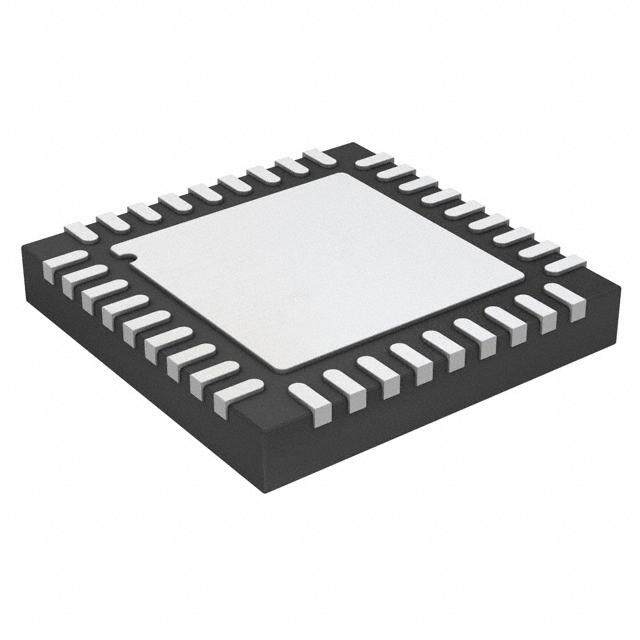
| 描述 | IC MIXER 400MHZ-3.7GHZ DWN 16QFN |
| 产品分类 | |
| 品牌 | Linear Technology |
| 数据手册 | http://www.linear.com/docs/7797 |
| 产品图片 |
|
| 产品型号 | LT5527EUF#PBF |
| RF类型 | 手机,GSM,MMDS,TD-SCDMA,UMTS,WCDMA |
| rohs | 无铅 / 符合限制有害物质指令(RoHS)规范要求 |
| 产品系列 | LT5527 |
| 产品目录页面 | |
| 供应商器件封装 | 16-QFN(4x4) |
| 其它名称 | LT5527EUFPBF |
| 包装 | 管件 |
| 噪声系数 | 12.5dB |
| 增益 | 2.3dB |
| 封装/外壳 | 16-WQFN 裸露焊盘 |
| 标准包装 | 91 |
| 混频器数 | 1 |
| 电压-电源 | 4.5 V ~ 5.25 V |
| 电流-电源 | 88mA |
| 辅助属性 | 降频变频器 |
| 频率 | 400MHz ~ 3.7GHz |


- 商务部:美国ITC正式对集成电路等产品启动337调查
- 曝三星4nm工艺存在良率问题 高通将骁龙8 Gen1或转产台积电
- 太阳诱电将投资9.5亿元在常州建新厂生产MLCC 预计2023年完工
- 英特尔发布欧洲新工厂建设计划 深化IDM 2.0 战略
- 台积电先进制程称霸业界 有大客户加持明年业绩稳了
- 达到5530亿美元!SIA预计今年全球半导体销售额将创下新高
- 英特尔拟将自动驾驶子公司Mobileye上市 估值或超500亿美元
- 三星加码芯片和SET,合并消费电子和移动部门,撤换高东真等 CEO
- 三星电子宣布重大人事变动 还合并消费电子和移动部门
- 海关总署:前11个月进口集成电路产品价值2.52万亿元 增长14.8%


PDF Datasheet 数据手册内容提取
LT5527 400MHz to 3.7GHz 5V High Signal Level Downconverting Mixer FEATURES DESCRIPTION n 50Ω Single-Ended RF and LO Ports The LT®5527 active mixer is optimized for high linearity, n Wide RF Frequency Range: 400MHz to 3.7GHz* wide dynamic range downconverter applications. The n High Input IP3: 24.5dBm at 900MHz IC includes a high speed differential LO buffer amplifi er 23.5dBm at 1900MHz driving a double-balanced mixer. Broadband, integrated n Conversion Gain: 3.2dB at 900MHz transformers on the RF and LO inputs provide single-ended 2.3dB at 1900MHz 50Ω interfaces. The differential IF output allows convenient n Integrated LO Buffer: Low LO Drive Level interfacing to differential IF fi lters and amplifi ers, or is n High LO-RF and LO-IF Isolation easily matched to drive 50Ω single-ended, with or without n Low Noise Figure: 11.6dB at 900MHz an external transformer. 12.5dB at 1900MHz The RF input is internally matched to 50Ω from 1.7GHz n Very Few External Components to 3GHz, and the LO input is internally matched to 50Ω n Enable Function from 1.2GHz to 5GHz. The frequency range of both ports n 4.5V to 5.25V Supply Voltage Range is easily extended with simple external matching. The IF n 16-Lead (4mm × 4mm) QFN Package output is partially matched and usable for IF frequencies up to 600MHz. APPLICATIONS The LT5527’s high level of integration minimizes the total n Cellular, WCDMA, TD-SCDMA and UMTS solution cost, board space and system-level variation. Infrastructure L, LT, LTC and LTM are registered trademarks of Linear Technology Corporation. n GSM900/GSM1800/GSM1900 Infrastructure All other trademarks are the property of their respective owners. *Operation over a wider frequency range is possible with reduced performance. Consult factory n 900MHz/2.4GHz/3.5GHz WLAN for information and assistance. n MMDS, WiMAX n High Linearity Downmixer Applications TYPICAL APPLICATION High Signal Level Downmixer for Multi-Carrier Wireless Infrastructure 1.9GHz Conversion Gain, IIP3, SSB NF and LO-RF Leakage vs LO Power LO INPUT –3dBm (TYP) 24 –20 22 IIP3 –25 LT5527 20 –30 m) IF = 240MHz dB 18 LOW SIDE LO –35LO IF+ 1040.7npHF 1nF B NF (dB), IIP3 ( 11114602 SSB NF TVAC C= =2 55°VC ––––44555050-RF LEAKAGE (d IF S B RF RF 220nH4.7pF O24U0TMPUHTz G, SC 68 LO-RF ––6650m) INPUT BIAS IF– 4 GC –70 2 –75 100nH –9 –7 –5 –3 –1 1 3 GND EN VCC2 VCC1 LO POWER (dBm) 5V 5527 TA01b 1nF 1μF 5527 TA01a 5527fa 1
LT5527 ABSOLUTE MAXIMUM RATINGS PIN CONFIGURATION (Note 1) TOP VIEW Supply Voltage (V , V , IF+, IF–) .......................5.5V CC1 CC2 C O C C N L N N Enable Voltage ................................–0.3V to V + 0.3V CC 16 15 14 13 LO Input Power (380MHz to 4GHz) ......................10dBm NC 1 12 GND LO Input DC Voltage ..............................–1V to V + 1V NC 2 11 IF+ CC 17 Continuous RF Input Power RF 3 10 IF– (400MHz to 4GHz) ...............................................12dBm NC 4 9 GND 5 6 7 8 RF Input Power (400MHz to 4GHz) ......................15dBm RF Input DC Voltage ...............................................±0.1V EN VCC2 VCC1 NC UF PACKAGE Operating Temperature Range ................–40°C to 85°C 16-LEAD (4mm (cid:115) 4mm) PLASTIC QFN Storage Temperature Range ...................–65°C to 125°C TJMAX = 125°C, θJA = 37°C/W EXPOSED PAD (PIN 17) IS GND, MUST BE SOLDERED TO PCB Junction Temperature (T ) ...................................125°C J ORDER INFORMATION LEAD FREE FINISH TAPE AND REEL PART MARKING PACKAGE DESCRIPTION TEMPERATURE RANGE LT5527EUF#PBF LT5527EUF#TRPBF 5527 16-Lead (4mm × 4mm) Plastic QFN –40°C to 85°C Consult LTC Marketing for parts specifi ed with wider operating temperature ranges. Consult LTC Marketing for information on non-standard lead based fi nish parts. For more information on lead free part marking, go to: http://www.linear.com/leadfree/ For more information on tape and reel specifi cations, go to: http://www.linear.com/tapeandreel/ DC ELECTRICAL CHARACTERISTICS V = 5V, EN = High, T = 25°C, unless otherwise specifi ed. Test CC A circuit shown in Figure 1. (Note 3) PARAMETER CONDITIONS MIN TYP MAX UNITS Power Supply Requirements (V ) CC Supply Voltage 4.5 5 5.25 VDC Supply Current V (Pin 7) 23.2 mA CC1 V (Pin 6) 2.8 mA CC2 IF+ + IF– (Pin 11 + Pin 10) 52 60 mA Total Supply Current 78 88 mA Enable (EN) Low = Off, High = On Shutdown Current EN = Low 100 μA Input High Voltage (On) 3 VDC Input Low Voltage (Off) 0.3 VDC EN Pin Input Current EN = 5VDC 50 90 μA Turn-ON Time 3 μs Turn-OFF Time 3 μs AC ELECTRICAL CHARACTERISTICS Test circuit shown in Figure 1. (Notes 2, 3) PARAMETER CONDITIONS MIN TYP MAX UNITS RF Input Frequency Range No External Matching (Midband) 1700 to 3000 MHz With External Matching (Low Band or High Band) 400 3700 MHz LO Input Frequency Range No External Matching 1200 to 3500 MHz With External Matching 380 MHz IF Output Frequency Range Requires Appropriate IF Matching 0.1 to 600 MHz 5527fa 2
LT5527 AC ELECTRICAL CHARACTERISTICS Test circuit shown in Figure 1. (Notes 2, 3) PARAMETER CONDITIONS MIN TYP MAX UNITS RF Input Return Loss Z = 50Ω, 1700MHz to 3000MHz >10 dB O LO Input Return Loss Z = 50Ω, 1200MHz to 3400MHz >12 dB O IF Output Impedance Differential at 240MHz 407Ω||2.5pF R||C LO Input Power 1200MHz to 3500MHz –8 –3 2 dBm 380MHz to 1200MHz –5 0 5 dBm Standard Downmixer Application: V = 5V, EN = High, T = 25°C, P = –5dBm (–5dBm/tone for 2-tone IIP3 tests, Δf = 1MHz), f = f CC A RF LO RF – f , P = –3dBm (0dBm for 450MHz and 900MHz tests), IF output measured at 240MHz, unless otherwise noted. Test circuit shown IF LO in Figure 1. (Notes 2, 3, 4) PARAMETER CONDITIONS MIN TYP MAX UNITS Conversion Gain RF = 450MHz, IF = 140MHz, High Side LO 2.5 dB RF = 900MHz, IF = 140MHz 3.4 dB RF = 1700MHz 2.3 dB RF = 1900MHz 2.3 dB RF = 2200MHz 2.0 dB RF = 2650MHz 1.8 dB RF = 3500MHz, IF = 380MHz 0.3 dB Conversion Gain vs Temperature T = –40°C to 85°C, RF = 1900MHz –0.018 dB/°C A Input 3rd Order Intercept RF = 450MHz, IF = 140MHz, High Side LO 23.2 dBm RF = 900MHz, IF = 140MHz 24.5 dBm RF = 1700MHz 24.2 dBm RF = 1900MHz 23.5 dBm RF = 2200MHz 22.7 dBm RF = 2650MHz 20.8 dBm RF = 3500MHz, IF = 380MHz 18.2 dBm Single-Sideband Noise Figure RF = 450MHz, IF = 140MHz, High Side LO 13.3 dB RF = 900MHz, IF = 140MHz 11.6 dB RF = 1700MHz 12.1 dB RF = 1900MHz 12.5 dB RF = 2200MHz 13.2 dB RF = 2650MHz 13.9 dB RF = 3500MHz, IF = 380MHz 16.1 dB LO to RF Leakage f = 400MHz to 2100MHz ≤–44 dBm LO f = 2100MHz to 3200MHz ≤–36 dBm LO LO to IF Leakage f = 400MHz to 700MHz ≤–40 dBm LO f = 700MHz to 3200MHz ≤–50 dBm LO RF to LO Isolation f = 400MHz to 2200MHz >43 dB RF f = 2200MHz to 3700MHz >38 dB RF RF to IF Isolation f = 400MHz to 800MHz >42 dB RF f = 800MHz to 3700MHz >54 dB RF 2RF-2LO Output Spurious Product 900MHz: f = 830MHz at –5dBm, f = 140MHz –60 dBc RF IF (f = fLO + f /2) 1900MHz: f = 1780MHz at –5dBm, f = 240MHz –65 dBc RF IF RF IF 3RF-3LO Output Spurious Product 900MHz: f = 806.67MHz at –5dBm, f = 140MHz –73 dBc RF IF (f = fLO + f /3) 1900MHz: f = 1740MHz at –5dBm, f = 240MHz –63 dBc RF IF RF IF Input 1dB Compression RF = 450MHz, IF = 140MHz, High Side 9.5 dBm LO RF = 900MHz, IF = 140MHz 8.9 dBm RF = 1900MHz 9.0 dBm Note 1: Stresses beyond those listed under Absolute Maximum Ratings Note 3: Specifi cations over the –40°C to 85°C temperature range are may cause permanent damage to the device. Exposure to any Absolute assured by design, characterization and correlation with statistical process Maximum Rating condition for extended periods may affect device controls. reliability and lifetime. Note 4: SSB Noise Figure measurements performed with a small-signal Note 2: 450MHz, 900MHz and 3500MHz performance measured with noise source and bandpass fi lter on RF input, and no other RF signal external LO and RF matching. See Figure 1 and Applications Information. applied. 5527fa 3
LT5527 TYPICAL AC PERFORMANCE CHARACTERISTICS Midband (No external RF/LO matching) V = 5V, EN = High, P = –5dBm (–5dBm/tone for 2-tone IIP3 tests, Δf = 1MHz), P = –3dBm, IF output measured at 240MHz, unless CC RF LO otherwise noted. Test circuit shown in Figure 1. Conversion Gain, IIP3 and NF vs RF Frequency LO Leakage vs LO Frequency RF Isolation vs RF Frequency 24 –30 –30 22 IIP3 –35 TPAL O= =2 5–°3CdBm –35 TA = 25°C 20 –40 –40 SB NF (dB), IIP3 (dBm) 11111648820 SSB NF TIFA = = 2 2450°MCHz O LEAKAGE (dBm)––––––476565500055 LO-RF LO-IF ISOLATION (dB) ––––––554766055005 RF-IF RF-LO S LOW SIDE LO L , C 6 HIGH SIDE LO –75 –75 G 4 –80 –80 GC 2 –85 –85 0 –90 –90 1700 1900 2100 2300 2500 2700 1200 1500 1800 2100 2400 2700 3000 1700 1900 2100 2300 2500 2700 RF FREQUENCY (MHz) LO FREQUENCY (MHz) RF FREQUENCY (MHz) 5527 G01 5527 G02 5527 G03 Conversion Gain and IIP3 Conversion Gain and IIP3 1900MHz Conversion Gain, IIP3 vs Temperature (Low Side LO) vs Temperature (High Side LO) and NF vs Supply Voltage 25 10 25 10 24 IIP3 IIP3 24 9 24 9 22 IIP3 20 LOW SIDE LO 23 8 23 8 m) IF = 240MHz 22 7 22 7 3 (dB 1186 –2450°C°C IIP3 (dBm)122910 I112F792 =000 0002MMM40HHHMzzzHz 465CG (dB) IIP3 (dBm)122910 I112F792 =000 0002MMM40HHHMzzzHz 465CG (dB) SB NF (dB), IIP 1114082 SSB NF 85°C 18 3 18 3 S , C 6 17 2 17 2 G GC GC GC 4 16 1 16 1 2 15 0 15 0 0 –50 –25 0 25 50 75 100 –50 –25 0 25 50 75 100 4.5 4.75 5 5.25 5.5 TEMPERATURE (°C) TEMPERATURE (°C) SUPPLY VOLTAGE (V) 5527 G04 5527 G05 5527 G06 1700MHz Conversion Gain, IIP3 1900MHz Conversion Gain, IIP3 2200MHz Conversion Gain, IIP3 and NF vs LO Power and NF vs LO Power and NF vs LO Power 25 24 24 23 22 22 IIP3 IIP3 LOW SIDE LO 21 LOW SIDE LO 20 IF = 240MHz 20 IIP3 m) 19 IF = 240MHz m) 18 –40°C m) 18 NF (dB), IIP3 (dB 11113715 SSB NF –284550°°CC°C NF (dB), IIP3 (dB 11112604 SSB NF 2855°°CC NF (dB), IIP3 (dB 11112604 SSB NF LIFO =W 2 S40IDMEH LzO SB 9 SB 8 SB 8 –40°C G, SC 57 GC G, SC 46 GC G, SC 46 GC 2855°°CC 3 2 2 1 0 0 –9 –7 –5 –3 –1 1 3 –9 –7 –5 –3 –1 1 3 –9 –7 –5 –3 –1 1 3 LO INPUT POWER (dBm) LO INPUT POWER (dBm) LO INPUT POWER (dBm) 5527 G07 5527 G08 5527 G09 5527fa 4
LT5527 TYPICAL AC PERFORMANCE CHARACTERISTICS Midband (No external RF/LO matching) V = 5V, EN = High, P = –5dBm (–5dBm/tone for 2-tone IIP3 tests, Δf = 1MHz), P = –3dBm, IF output measured at 240MHz, unless CC RF LO otherwise noted. Test circuit shown in Figure 1. IF Output Power, IM3 and IM5 vs IF , 2 × 2 and 3 × 3 Spurs 2 × 2 and 3 × 3 Spurs OUT RF Input Power (2 Input Tones) vs RF Input Power (Single Tone) vs LO Power (Single Tone) 10 15 –50 TA = 25°C 0 5 LO = 1660MHz –55 m)–10 IFOUT –5 IF = 240MHz IFOUT c)–60 (RF 3=R 1F7-34L0OMHz) WER/TONE (dB––––53240000 TRRLAOFF 12 == == 21 5116°896C90090M..55HMMzHHzz POWER (dBm) ––––31425555 (RF = 1900MHz) PUR LEVEL (dB–––776055 (RF 2=R 1F7-28L0OMHz) OUTPUT PO–––678000 IM3 OUTPUT –––576555 (RF = 1734R0FM-3HLzO) 2(RRFF -=2 L1O780MHz) RELATIVE S–––889050 TLAO == 2156°6C0MHz –90 –85 –95 IF = 240MHz IM5 PRF = –5dBm –100 –95 –100 –21 –18 –15 –12 –9 –6 –3 0 –18–15–12 –9 –6 –3 0 3 6 9 12 –9 –7 –5 –3 –1 1 3 RF INPUT POWER (dBm/TONE) 5527 G10 RF INPUT POWER (dBm) 5527 G11 LO INPUT POWER (dBm) 5527 G12 High Band (3500MHz application with external RF matching) V = 5V, EN = High, P = –5dBm (–5dBm/tone for 2-tone IIP3 tests, CC RF Δf = 1MHz), low side LO, P = –3dBm, IF output measured at 380MHz, unless otherwise noted. Test circuit shown in Figure 1. LO Conversion Gain, IIP3 and SSB 3500MHz Conversion Gain, IIP3 LO Leakage and RF-LO Isolation NF vs RF Frequency and SSB NF vs LO Power vs LO and RF Frequency 20 19 –20 60 IIP3 18 IIP3 17 SSB NF , SSB NF (dB), IIP3 (dBm)C 1111268046 SSB NF LITFOA = W= 3 2S850I°DMCEH LzO , SSB NF (dB), IIP3 (dBm)C 111715593 LITFOA = W= 3 2S850I°DMCEH LzO LO LEAKAGE (dBm)–––543000 LO-RF RF-LO 345000RF-LO ISOLATION (dB) G 4 G 3 –60 20 GC LO-IF 2 1 GC 0 –1 –70 10 3300 3400 3500 3600 3700 –9 –7 –5 –3 –1 1 3 3000 3200 3400 3600 3800 RF FREQUENCY (MHz) 5527 G13 LO INPUT POWER (dBm) 5527 G14 LO/RF FREQUENCY (MHz) 5527 G15 Low Band (450MHz application with external RF/LO matching) V = 5V, EN = High, P = –5dBm (–5dBm/tone for 2-tone IIP3 tests, CC RF Δf = 1MHz), P = 0dBm, IF output measured at 140MHz, unless otherwise noted. Test circuit shown in Figure 1. LO Conversion Gain, IIP3 and NF 450MHz Conversion Gain, vs RF Frequency IIP3 and NF vs LO Power LO Leakage vs LO Frequency 24 24 –20 TA = 25°C Bm) 122802 IIP3 HTIFAI G= = H1 2 4S50I°DMCEH LzO Bm) 221028 IIP3 HI–F4I G=0 H°1C 4S0IDMEH LzO –30 PL(O4 5=0 0MLdOHB-zmIF APP) LO-RF SB NF (dB), IIP3 (d 111164082 SSB NF SB NF (dB), IIP3 (d 111182604 SSB NF 2855°°CC O LEAKAGE (dBm)–––654000 (450LMOH-Rz FAPP) (900MHz APP) S S L LO-IF G, C 6 G, C 6 GC (900MHz APP) 4 4 –70 2 2 GC 0 0 –80 400 425 450 475 500 –6 –4 –2 0 2 4 6 400 600 800 1000 1200 RF FREQUENCY (MHz) 5527 G18 LO INPUT POWER (dBm) 5527 G19 LO FREQUENCY (MHz) 5527 G20 5527fa 5
LT5527 TYPICAL AC PERFORMANCE CHARACTERISTICS Low Band (900MHz application with external RF/LO matching) V = 5V, EN = High, P = –5dBm (–5dBm/tone for 2-tone IIP3 tests, Δf = 1MHz), P = 0dBm, IF output measured at CC RF LO 140MHz, unless otherwise noted. Test circuit shown in Figure 1. Conversion Gain, IIP3 and NF vs RF Frequency (900MHz Low Side 900MHz Conversion Gain, IIP3 and IF , 2 × 2 and 3 × 3 Spurs OUT Application) NF vs LO Power (Low Side LO) vs RF Input Power (Single Tone) 25 25 20 IIP3 TA = 25°C 23 23 IIP3 LOW SIDE LO 10 LO = 760MHz 21 21 IF = 140MHz 0 IF = 140MHz dB), IIP3 (dBm) 11119375 LTIFOA = W= 1 2S450I°DMCEH LzO dB), IIP3 (dBm) 11119375 SSB NF –284550°°CC°C OWER (dBm) ––––23140000 I(FROFU =T 900MHz) SB NF ( 191 SSB NF SB NF ( 191 TPUT P ––6500 (RF = 823R0FM-2HLzO) S S U , C 7 , C 7 O –70 G G GC 3RF-3LO 5 5 –80 GC (RF = 806.67MHz) 3 3 –90 1 1 –100 750 800 850 900 950 1000 1050 –6 –4 –2 0 2 4 6 –18–15–12 –9 –6 –3 0 3 6 9 12 RF FREQUENCY (MHz) LO INPUT POWER (dBm) RF INPUT POWER (dBm) 5527 G21 5527 G22 5527 G23 Conversion Gain, IIP3 and NF vs RF Frequency (900MHz High Side 900MHz Conversion Gain, IIP3 and 2 × 2 and 3 × 3 Spurs Application) NF vs LO Power (High Side LO) vs LO Power (Single Tone) 25 25 –40 23 IIP3 23 TA = 25°C IIP3 –45 LO = 760MHz 21 21 IF = 140MHz G, SSB NF (dB), IIP3 (dBm)C 1111159937715 SSB NF HTIFAI G= = H1 2 4S50I°DMCEH LzO G, SSB NF (dB), IIP3 (dBm)C 1111159937715 GSSCB NF HI–28F455I G=0°°CC H°1C 4S0IDMEH LzO RELATIVE SPUR LEVEL (dBc)–––––––76576580005550 PRF = –5dBm(RF =3 R80F6-3.6L7OM(RHFz2 )=R F8-320LMOHz) 3 GC 3 –85 1 1 –90 750 800 850 900 950 1000 1050 –6 –4 –2 0 2 4 6 –6 –4 –2 0 2 4 6 RF FREQUENCY (MHz) LO INPUT POWER (dBm) LO INPUT POWER (dBm) 5527 G24 5527 G25 5527 G26 TYPICAL DC PERFORMANCE CHARACTERISTICS Test circuit shown in Figure 1. Supply Current vs Supply Voltage Shutdown Current vs Supply Voltage 82 100 81 80 CURRENT (mA) 777869 82055°°°CCC 60°C N CURRENT (μA) 10 LY 75 –40°C OW 85°C P D 1 UP 74 UT S H 60°C 25°C 73 S 72 –40°C 0°C 71 0.1 4.5 4.75 5 5.25 5.5 4.5 4.75 5 5.25 5.5 SUPPLY VOLTAGE (V) 5527 G16 SUPPLY VOLTAGE (V) 5527 G17 5527fa 6
LT5527 PIN FUNCTIONS NC (Pins 1, 2, 4, 8, 13, 14, 16): Not Connected Internally. be externally connected to the V pin and decoupled CC2 These pins should be grounded on the circuit board for with 1000pF and 1μF capacitors. improved LO-to-RF and LO-to-IF isolation. GND (Pins 9, 12): Ground. These pins are internally RF (Pin 3): Single-Ended Input for the RF Signal. This pin connected to the backside ground for improved isola- is internally connected to the primary side of the RF input tion. They should be connected to the RF ground on the transformer, which has low DC resistance to ground. If circuit board, although they are not intended to replace the RF source is not DC blocked, then a series blocking the primary grounding through the backside contact of capacitor must be used. The RF input is internally matched the package. from 1.7GHz to 3GHz. Operation down to 400MHz or up IF–, IF+ (Pins 10, 11): Differential Outputs for the IF to 3700MHz is possible with simple external matching. Signal. An impedance transformation may be required to EN (Pin 5): Enable Pin. When the input enable voltage is match the outputs. These pins must be connected to V CC higher than 3V, the mixer circuits supplied through Pins 6, through impedance matching inductors, RF chokes or a 7, 10 and 11 are enabled. When the input voltage is less transformer center tap. than 0.3V, all circuits are disabled. Typical input current LO (Pin 15): Single-Ended Input for the Local Oscillator is 50μA for EN = 5V and 0μA when EN = 0V. The EN pin Signal. This pin is internally connected to the primary side should not be left fl oating. Under no conditions should the of the LO transformer, which is internally DC blocked. An EN pin voltage exceed V + 0.3V, even at start-up. CC external blocking capacitor is not required. The LO input is V (Pin 6): Power Supply Pin for the Bias Circuits. internally matched from 1.2GHz to 5GHz. Operation down CC2 Typical current consumption is 2.8mA. This pin should to 380MHz is possible with simple external matching. be externally connected to the V pin and decoupled CC1 Exposed Pad (Pin 17): Circuit Ground Return for the with 1000pF and 1μF capacitors. Entire IC. This must be soldered to the printed circuit V (Pin 7): Power Supply Pin for the LO Buffer Circuits. board ground plane. CC1 Typical current consumption is 23.2mA. This pin should BLOCK DIAGRAM 15 LO REGULATOR VCC1 LAIMMPITLIINFIGERS EXPOPSAEDD 17 GND 12 LINEAR AMPLIFIER IF+ 11 RF IF– 3 10 DOUBLE-BALANCED MIXER GND 9 BIAS EN VCC2 VCC1 5 6 7 5527 BD 5527fa 7
LT5527 TEST CIRCUITS LOIN L4 0.018" (cid:69)R = 4.4 RF GND C4 0.062" BIAS 16 15 14 13 0.018" GND EXTERNAL MATCHING NC LO NC NC FOR LOW FREQUENCY 1 12 NC GND T1 LO ONLY L1 2 + 11 3 • • 4 NC IF RFIN 5Z0OΩ LT5527 C3 2 3 RF IF– 10 1 5 I2F4O0UMTHz L (mm) 4 9 L2 NC GND C5 EXTERNAL MATCHING EN VCC2 VCC1 NC FOR LOW BAND OR 5 6 7 8 HIGH BAND ONLY EN VCC APPLICATION LO MATCH RF MATCH C1 C2 GND RF LO L4 C4 L C5 5527 F01 450MHz High Side 6.8nH 10pF 4.5mm 12pF 900MHz Low Side 3.9nH 5.6pF 1.3mm 3.9pF 900MHz High Side — 2.7pF 1.3mm 3.9pF 3500MHz Low Side — — 4.5mm 0.5pF REF DES VALUE SIZE PART NUMBER REF DES VALUE SIZE PART NUMBER C1 1000pF 0402 AVX 04025C102JAT L4, C4, C5 0402 See Applications Information C2 1μF 0603 AVX 0603ZD105KAT L1, L2 82nH 0603 Toko LLQ1608-A82N C3 2.7pF 0402 AVX 04025A2R7CAT T1 4:1 M/A-Com ETC4-1-2 (2MHz to 800MHz) Figure 1. Downmixer Test Schematic—Standard IF Matching (240MHz IF) LOIN L4 C4 DISCRETE IF BALUN 16 15 14 13 EXTERNAL MATCHING NC LO NC NC FOR LOW FREQUENCY 1 12 C6 NC GND LO ONLY 2 + 11 NC IF L1 C3 RFIN 5Z0OΩ 3 RF LT5527 IF– 10 L3 C7 I2F4O0UMTHz L (mm) 4 9 NC GND C5 EXTERNAL MATCHING EN VCC2 VCC1 NC L2 FOR LOW BAND OR 5 6 7 8 HIGH BAND ONLY EN VCC C1 C2 GND 5527 F02 REF DES VALUE SIZE PART NUMBER REF DES VALUE SIZE PART NUMBER C1, C3 1000pF 0402 AVX 04025C102JAT L4, C4, C5 0402 See Applications Information C2 1μF 0603 AVX 0603ZD105KAT L1, L2 100nH 0603 Toko LLQ1608-AR10 C6, C7 4.7pF 0402 AVX 04025A4R7CAT L3 220nH 0603 Toko LLQ1608-AR22 Figure 2. Downmixer Test Schematic—Discrete IF Balun Matching (240MHz IF) 5527fa 8
LT5527 APPLICATIONS INFORMATION Introduction at Pin 3, which improves the 1.7GHz return loss to greater than 20dB. Likewise, the 2.7GHz match can be improved The LT5527 consists of a high linearity double-balanced to greater than 30dB with a series 1.5nH inductor. A series mixer, RF buffer amplifi er, high speed limiting LO buffer 1.5nH/2.7pF network will simultaneously optimize the lower amplifi er and bias/enable circuits. The RF and LO inputs and upper band edges and expand the RF input bandwidth are both single ended. The IF output is differential. Low to 1.1GHz-3.3GHz. Measured RF input return losses for side or high side LO injection can be used. these three cases are also plotted in Figure 4a. Two evaluation circuits are available. The standard evalua- Alternatively, the input match can be shifted down, as low tion circuit, shown in Figure 1, incorporates transformer- as 400MHz or up to 3700MHz, by adding a shunt capacitor based IF matching and is intended for applications that (C5) to the RF input. A 450MHz input match is realized with require the lowest LO-IF leakage levels and the widest C5 = 12pF, located 4.5mm away from Pin 3 on the evaluation IF bandwidth. The second evaluation circuit, shown in board’s 50Ω input transmission line. A 900MHz input match Figure 2, replaces the IF transformer with a discrete IF requires C5 = 3.9pF, located at 1.3mm. A 3500MHz input balun for reduced solution cost and size. The discrete match is realized with C5 = 0.5pF, located at 4.5mm. This IF balun delivers comparable noise fi gure and linearity, higher conversion gain, but degraded LO-IF leakage and 0 reduced IF bandwidth. NO EXTERNAL –5 RF Input Port dB) MATCHING SS (–10 O The mixer’s RF input, shown in Figure 3, consists of an L N integrated transformer and a high linearity differential UR–15 T E amplifi er. The primary terminals of the transformer are RT R–20 connected to the RF input pin (Pin 3) and ground. The PO SERIES 1.5nH F SERIES 2.7pF SERIES 2.7pF R secondary side of the transformer is internally connected –25 to the amplifi er’s differential inputs. SERIES 1.5nH –30 0.2 0.7 1.2 1.7 2.2 2.7 3.2 3.7 4.2 One terminal of the transformer’s primary is internally FREQUENCY (GHz) grounded. If the RF source has DC voltage present, then 5527 F04a a coupling capacitor must be used in series with the RF (4a) Series Reactance Matching input pin. 0 The RF input is internally matched from 1.7GHz to 3GHz, requiring no external components over this frequency –5 B) range. The input return loss, shown in Figure 4a, is typi- d cally 10dB at the band edges. The input match at the lower OSS (–10 L N band edge can be optimized with a series 2.7pF capacitor UR–15 ET NO EXTERNAL R RT –20 MATCHING PO 900MHz 3.5GHz EXTERNAL MATCHING RF 450MHz C5 = 3.9pF C5 = 0.5pF FOR LOW BAND OR –25 C5 = 12pF L = 1.3mm L = 4.5mm HIGH BAND ONLY TO L = 4.5mm RFIN LZ =O L= (5m0Ωm) MIXER –300.2 0.7 1.2 1.7 2.2 2.7 3.2 3.7 4.2 RF 3 RF FREQUENCY (GHz) C5 5527 F04b 5527 F03 (4b) Series Shunt Matching Figure 3. RF Input Schematic Figure 4. RF Input Return Loss With and Without External Matching 5527fa 9
LT5527 APPLICATIONS INFORMATION series transmission line/shunt capacitor matching topol- The LO input is internally matched from 1.2GHz to 5GHz, al- ogy allows the LT5527 to be used for multiple frequency though the maximum useful frequency is limited to 3.5GHz standards without circuit board layout modifi cations. The by the internal amplifi ers. The input match can be shifted series transmission line can also be replaced with a series down, as low as 750MHz, with a single shunt capacitor chip inductor for a more compact layout. (C4) on Pin 15. One example is plotted in Figure 6 where C4 = 2.7pF produces an 850MHz to 1.2GHz match. Input return loss for these three cases (450MHz, 900MHz and 3500MHz) are plotted in Figure 4b. The input return LO input matching below 750MHz requires the series induc- loss with no external matching is repeated in Figure 4b tor (L4)/shunt capacitor (C4) network shown in Figure 5. for comparison. Two examples are plotted in Figure 6 where L4 = 3.9nH/C4 = 5.6pF produces a 650MHz to 830MHz match and L4 = RF input impedance and S11 versus frequency (with no 6.8nH/C4 = 10pF produces a 540MHz to 640MHz match. external matching) is listed in Table 1 and referenced to The evaluation boards do not include pads for L4, so the Pin 3. The S11 data can be used with a microwave circuit circuit trace needs to be cut near Pin 15 to insert L4. A low simulator to design custom matching networks and simu- cost multilayer chip inductor is adequate for L4. late board-level interfacing to the RF input fi lter. The optimum LO drive is –3dBm for LO frequencies above Table 1. RF Input Impedance vs Frequency 1.2GHz, although the amplifi ers are designed to accom- FREQUENCY INPUT S11 modate several dB of LO input power variation without (MHz) IMPEDANCE MAG ANGLE signifi cant mixer performance variation. Below 1.2GHz, 50 4.8 + j2.6 0.825 173.9 300 9.0 + j11.9 0.708 152.5 EXTERNAL 450 11.9 + j15.3 0.644 144.3 MATCHING FOR LOW BAND 600 14.3 + j18.2 0.600 137.2 ONLY TO 900 19.4 + j23.8 0.529 123.2 MIXER 1200 26.1 + j29.8 0.467 107.4 LOIN L4 LO 15 1500 37.3 + j33.9 0.386 89.3 C4 VBIAS LIMITER 1850 57.4 + j29.7 0.275 60.6 2150 71.3 + j10.1 0.193 20.6 VCC2 2450 64.6 – j13.9 0.175 –36.8 5527 F05 2650 53.0 – j21.8 0.209 –70.3 Figure 5. LO Input Schematic 3000 35.0 – j21.2 0.297 –111.2 3500 20.7 – j9.0 0.431 –155.8 0 4000 14.2 + j6.2 0.564 164.8 5000 10.4 + j31.9 0.745 113.3 B) –5 L4 = 6.8nH LC44 == 02n.7HpF d C4 = 10pF S (–10 S O LO Input Port N L NO R–15 EXTERNAL U T MATCHING The mixer’s LO input, shown in Figure 5, consists of an RE integrated transformer and high speed limiting differential ORT –20 LC44 == 35..96npHF P O amplifi ers. The amplifi ers are designed to precisely drive L–25 the mixer for the highest linearity and the lowest noise –30 fi gure. An internal DC blocking capacitor in series with the 0.1 1 5 LO FREQUENCY (GHz) transformer’s primary eliminates the need for an external 5527 F06 blocking capacitor. Figure 6. LO Input Return Loss 5527fa 10
LT5527 APPLICATIONS INFORMATION 0dBm LO drive is recommended for optimum noise fi gure, 8. Frequency-dependent differential IF output impedance although –3dBm will still deliver good conversion gain is listed in Table 3. This data is referenced to the package and linearity. pins (with no external components) and includes the ef- fects of IC and package parasitics. The IF output can be Custom matching networks can be designed using the port matched for IF frequencies as low as several kHz or as impedance data listed in Table 2. This data is referenced high as 600MHz. to the LO pin with no external matching. Table 3. IF Output Impedance vs Frequency Table 2. LO Input Impedance vs Frequency DIFFERENTIAL OUTPUT FREQUENCY INPUT S11 FREQUENCY (MHz) IMPEDANCE (RIF || XIF) (MHz) IMPEDANCE MAG ANGLE 1 415||-j64k 50 30.4 – j355.7 0.977 –15.9 10 415||-j6.4k 300 8.7 – j52.2 0.847 –86.7 70 415||-j909 450 9.4 – j25.4 0.740 –124.8 140 413||-j453 600 11.5 – j8.9 0.635 –158.7 240 407||-j264 900 19.7 + j12.8 0.463 146.7 300 403||-j211 1200 34.3 + j24.3 0.330 106.9 380 395||-j165 1500 49.8 + j21.3 0.209 78.5 450 387||-j138 1850 53.8 + j8.9 0.093 61.7 500 381||-j124 2150 50.4 + j3.2 0.032 80.5 2450 45.1 + j0.3 0.052 176.5 The following three methods of differential to single-ended 2650 41.1 + j2.4 0.101 163.1 IF matching will be described: 3000 41.9 + j8.1 0.124 129.8 • Direct 8:1 transformer 3500 49.0 + j12.0 0.120 87.9 4000 55.4 + j8.6 0.096 53.2 • Lowpass matching + 4:1 transformer 5000 33.2 + j8.7 0.226 146.7 • Discrete IF balun IF Output Port The IF outputs, IF+ and IF–, are internally connected to the IF+ 11 L1 4:1 IFOUT 50Ω collectors of the mixer switching transistors (see Figure 7). C3 VCC Both pins must be biased at the supply voltage, which IF– can be applied through the center tap of a transformer or 10 L2 through matching inductors. Each IF pin draws 26mA of VCC supply current (52mA total). For optimum single-ended 5527 F07 performance, these differential outputs should be com- Figure 7. IF Output with External Matching bined externally through an IF transformer or a discrete IF balun circuit. The standard evaluation board (see Figure 1) includes an IF transformer for impedance transforma- tion and differential to single-ended transformation. A 0.7nH IF+ 11 second evaluation board (see Figure 2) realizes the same RS 2.5pF functionality with a discrete IF balun circuit. 415Ω IF– 10 The IF output impedance can be modeled as 415Ω in parallel 0.7nH with 2.5pF at low frequencies. An equivalent small-signal 5527 F08 model (including bondwire inductance) is shown in Figure Figure 8. IF Output Small-Signal Model 5527fa 11
LT5527 APPLICATIONS INFORMATION Direct 8:1 IF Transformer Matching frequencies are listed in Table 4. High-Q wire-wound chip inductors (L1 and L2) improve the mixer’s conversion gain For IF frequencies below 100MHz, the simplest IF matching by a few tenths of a dB, but have little effect on linearity. technique is an 8:1 transformer connected across the IF Measured output return losses for each case are plotted pins. The transformer will perform impedance transfor- in Figure 10 for the simple 8:1 transformer method and mation and provide a single-ended 50Ω output. No other for the lowpass/4:1 transformer method. matching is required. Measured performance using this technique is shown in Figure 9. This matching is easily Table 4. IF Matching Element Values implemented on the standard evaluation board by short- IF FREQUENCY L1, L2 C3 IF ing across the pads for L1 and L2 and replacing the 4:1 PLOT (MHz) (nH) (pF) TRANSFORMER transformer with an 8:1 (C3 not installed). 1 1 to 100 Short — TC8-1 (8:1) 2 140 120 — ETC4-1-2 (4:1) 25 3 190 110 2.7 ETC4-1-2 (4:1) 23 IIP3 4 240 82 2.7 ETC4-1-2 (4:1) B) 21 d RF = 900MHz 5 380 56 2.2 ETC4-1-2 (4:1) F ( 19 HIGH SIDE LO AT 0dBm N B 17 VCC = 5V DC 6 450 43 2.2 ETC4-1-2 (4:1) m), SS 15 TCA4 == 225.7°pCF, C5 = 3.9pF dB 13 SSB NF 0 3 ( 11 P G (dB), IIC 957 GC SS (dB)–1–05 3 O L 110 20 30 40 50 60 70 80 90 100 URN –15 T IF OUTPUT FREQUENCY (MHz) RE 5527 F09 RT –20 O P FSiSgBu rNeF 9 U. sTiynpgic aanl C8:o1n vIFe rTsriaonns fGoarmine, rIIP3 and IF –25 2 4 5 6 1 3 –30 Lowpass + 4:1 IF Transformer Matching 0 50 100 150200250300350400 450500 IF FREQUENCY (MHz) The lowest LO-IF leakage and wide IF bandwidth are real- 5527 F10 Figure 10. IF Output Return Losses ized by using the simple, three element lowpass matching with Lowpass/Transformer Matching network shown in Figure 7. Matching elements C3, L1 and L2, in conjunction with the internal 2.5pF capacitance, Discrete IF Balun Matching form a 400Ω to 200Ω lowpass matching network which For many applications, it is possible to replace the IF is tuned to the desired IF frequency. The 4:1 transformer transformer with the discrete IF balun shown in Figure 2. then transforms the 200Ω differential output to a 50Ω The values of L1, L2, C6 and C7 are calculated to realize single-ended output. a 180 degree phase shift at the desired IF frequency and This matching network is most suitable for IF frequencies provide a 50Ω single-ended output, using the equations above 40MHz or so. Below 40MHz, the value of the series listed below. Inductor L3 is calculated to cancel the in- inductors (L1 and L2) becomes unreasonably high, and ternal 2.5pF capacitance. L3 also supplies bias voltage could cause stability problems, depending on the induc- to the IF+ pin. Low cost multilayer chip inductors are tor value and parasitics. Therefore, the 8:1 transformer adequate for L1 and L2. A high Q wire-wound chip induc- technique is recommended for low IF frequencies. tor is recommended for L3 to maximize conversion gain Suggested lowpass matching element values for several IF and minimize DC voltage drop to the IF+ pin. C3 is a DC blocking capacitor. 5527fa 12
LT5527 APPLICATIONS INFORMATION R (cid:129)R 0 L1,L2= IF OUT ω IF –5 B) d C6,C7= 1 OSS (–10 L ω (cid:129) R (cid:129)R N IF IF OUT UR–15 T E R 190MHz L3= XIF ORT –20 P 240MHz 380MHz ω F IF I–25 450MHz Compared to the lowpass/4:1 transformer matching tech- –30 nique, this network delivers approximately 0.8dB higher 50 100150 200250300350400450 500550 conversion gain (since the IF transformer loss is elimi- IF FREQUENCY (MHz) 5527 F11 nated) and comparable noise fi gure and IIP3. At a ±15% Figure 11. IF Output Return Losses with Discrete Balun Matching offset from the IF center frequency, conversion gain and noise fi gure degrade about 1dB. Beyond ±15%, conver- 26 0 sion gain decreases gradually but noise fi gure increases 24 rapidly. IIP3 is less sensitive to bandwidth. Other than IF 22 IIP3 –10 bandwidth, the most signifi cant difference is LO-IF leakage, 20 L wtthraheni csshufo pdremergieorrar dmpeeasrt cftoohr imnapgap.nrcoex irmeaaltiezleyd – w38itdhB tmhe cloomwppaasresd/4 t:o1 B), IIP3 (dBm) 11118642 123494850000IIIIFFFF LTOA W= 2S5I°DCE LO (–3dBm) ––2300 O-IF LEAKAGE (dC 10 –40 (dB Discrete IF balun element values for four common IF fre- G LO-IF m 8 ) quencies are listed in Table 5. The corresponding measured 6 –50 GC IF output return losses are shown in Figure 11. The values 4 2 –60 listed in Table 5 differ from the calculated values slightly 1700 1900 2100 2300 2500 2700 due to circuit board and component parasitics. Typical RF INPUT FREQUENCY (MHz) 5527 F12 conversion gain, IIP3 and LO-IF leakage, versus RF input Figure 12. Conversion Gain, IIP3 and LO-IF Leakage vs RF Input frequency, for all four IF frequency examples is shown in Frequency Using Discrete IF Balun Matching Figure 12. Typical conversion gain, IIP3 and noise fi gure versus IF output frequency for the same circuits are shown 26 in Figure 13. 24 22 Table 5. Discrete IF Balun Element Values (ROUT = 50Ω) Bm) 20 IIP3 LOW SIDE LO (–3dBm) IF FREQUENCY L1, L2 C6, C7 L3 3 (d 18 TA = 25°C P 16 (MHz) (nH) (pF) (nH) B), II 14 129400 112000 64..87 222200 SB NF (d 1120 SSB NF 129400IIFF 380 56 3 68 G, SC 86 GC 348500IIFF 450 47 2.7 47 4 2 0 For fully differential IF architectures, the IF transformer can 150 200 250 300 350 400 450 500 550 be eliminated. An example is shown in Figure 14, where IF OUTPUT FREQUENCY (MHz) 5527 F13 the mixer’s IF output is matched directly into a SAW fi lter. Figure 13. Conversion Gain, IIP3 and SSB NF vs IF Output Supply voltage to the mixer’s IF pins is applied through Frequency Using Discrete IF Balun Matching 5527fa 13
LT5527 APPLICATIONS INFORMATION matching inductors in a band-pass IF matching network. The values of L1, L2 and C3 are calculated to resonate at IF+ L1 FSILATWER AMIFP the desired IF frequency with a quality factor that satisfi es C3 the required IF bandwidth. The L and C values are then adjusted to account for the mixer’s internal 2.5pF capaci- IF– L2 5527 F14 tance and the SAW fi lter’s input capacitance. In this case, the differential IF output impedance is 400Ω since the SUPPLY VCC bandpass network does not transform the impedance. DECOUPLING Additional matching elements may be required if the SAW Figure 14. Bandpass IF Matching for Differential IF Architectures fi lter’s input impedance is less than or greater than 400Ω. Contact the factory for application assistance. Standard Evaluation Board Layout Discrete IF Evaluation Board Layout 5527fa 14
LT5527 PACKAGE DESCRIPTION UF Package 16-Lead Plastic QFN (4mm × 4mm) (Reference LTC DWG # 05-08-1692) 0.72 ±0.05 4.35 ± 0.05 2.15 ± 0.05 2.90 ± 0.05 (4 SIDES) PACKAGE OUTLINE 0.30 ±0.05 0.65 BSC RECOMMENDED SOLDER PAD PITCH AND DIMENSIONS BOTTOM VIEW—EXPOSED PAD PIN 1 NOTCH R = 0.20 TYP 4.00 ± 0.10 0.75 ± 0.05 R = 0.115 OR 0.35 × 45° CHAMFER (4 SIDES) TYP 15 16 PIN 1 0.55 ± 0.20 TOP MARK (NOTE 6) 1 2 2.15 ± 0.10 (4-SIDES) (UF16) QFN 10-04 0.200 REF 0.30 ± 0.05 0.00 – 0.05 0.65 BSC NOTE: 1. DRAWING CONFORMS TO JEDEC PACKAGE OUTLINE MO-220 VARIATION (WGGC) 2. DRAWING NOT TO SCALE 3. ALL DIMENSIONS ARE IN MILLIMETERS 4. DIMENSIONS OF EXPOSED PAD ON BOTTOM OF PACKAGE DO NOT INCLUDE MOLD FLASH. MOLD FLASH, IF PRESENT, SHALL NOT EXCEED 0.15mm ON ANY SIDE 5. EXPOSED PAD SHALL BE SOLDER PLATED 6. SHADED AREA IS ONLY A REFERENCE FOR PIN 1 LOCATION ON THE TOP AND BOTTOM OF PACKAGE 5527fa Information furnished by Linear Technology Corporation is believed to be accurate and reliable. 15 However, no responsibility is assumed for its use. Linear Technology Corporation makes no representa- tion that the interconnection of its circuits as described herein will not infringe on existing patent rights.
LT5527 RELATED PARTS PART NUMBER DESCRIPTION COMMENTS Infrastructure LT5511 High Linearity Upconverting Mixer RF Output to 3GHz, 17dBm IIP3, Integrated LO Buffer LT5512 1kHz to 3GHz High Signal Level Active Mixer Optimized for HF/VHF/UHF Applications, 20dBm IIP3 11dB NF LT5514 Ultralow Distortion, IF Amplifi er/ADC Driver with 850MHz Bandwidth, 47dBm OIP3 at 100MHz, 10.5dB to 33dB Gain Control Range Digitally Controlled Gain LT5515 1.5GHz to 2.5GHz Direct Conversion Quadrature 20dBm IIP3, Integrated LO Quadrature Generator Demodulator LT5516 0.8GHz to 1.5GHz Direct Conversion Quadrature 21.5dBm IIP3, Integrated LO Quadrature Generator Demodulator LT5517 40MHz to 900MHz Quadrature Demodulator 21dBm IIP3, Integrated LO Quadrature Generator LT5519 0.7GHz to 1.4GHz High Linearity Upconverting Mixer 17.1dBm IIP3 at 1GHz, Integrated RF Output Transformer with 50Ω Matching, Single-Ended LO and RF Ports Operation LT5520 1.3GHz to 2.3GHz High Linearity Upconverting Mixer 15.9dBm IIP3 at 1.9GHz, Integrated RF Output Transformer with 50Ω Matching, Single-Ended LO and RF Ports Operation LT5521 10MHz to 3700MHz High Linearity 24.2dBm IIP3 at 1.95GHz, NF = 12.5dB, 3.15V to 5.25V Supply, Single-Ended Upconverting Mixer LO Port Operation LT5522 400MHz to 2.7GHz High Signal Level 4.5V to 5.25V Supply, 25dBm IIP3 at 900MHz, NF = 12.5dB, 50Ω Single-Ended RF Downconverting Mixer and LO Ports LT5524 Low Power, Low Distortion ADC Driver with Digitally 450MHz Bandwidth, 40dBm OIP3, 4.5dB to 27dB Gain Control Programmable Gain LT5525 High Linearity, Low Power Downconverting Mixer Single-Ended 50Ω RF and LO Ports, 17.6dBm IIP3 at 1900MHz, I = 28mA CC LT5526 High Linearity, Low Power Downconverting Mixer 3V to 5.3V Supply, 16.5dBm IIP3, 100kHz to 2GHz RF, NF = 11dB, I = 28mA, CC –65dBm LO-RF Leakage LT5557 400MHz to 3.8GHz, 3.3V High Signal Level Single-Ended RF and LO Ports, 24.7dBm IIP3 at 1950MHz, NF = 11.7dB Downconverting Mixer RF Power Detectors LT5504 800MHz to 2.7GHz RF Measuring Receiver 80dB Dynamic Range, Temperature Compensated, 2.7V to 5.25V Supply LTC®5505 RF Power Detectors with >40dB Dynamic Range 300MHz to 3GHz, Temperature Compensated, 2.7V to 6V Supply LTC5507 100kHz to 1000MHz RF Power Detector 100kHz to 1GHz, Temperature Compensated, 2.7V to 6V Supply LTC5508 300MHz to 7GHz RF Power Detector 44dB Dynamic Range, Temperature Compensated, SC70 Package LTC5509 300MHz to 3GHz RF Power Detector 36dB Dynamic Range, Low Power Consumption, SC70 Package LTC5530 300MHz to 7GHz Precision RF Power Detector Precision V Offset Control, Shutdown, Adjustable Gain OUT LTC5531 300MHz to 7GHz Precision RF Power Detector Precision V Offset Control, Shutdown, Adjustable Offset OUT LTC5532 300MHz to 7GHz Precision RF Power Detector Precision V Offset Control, Adjustable Gain and Offset OUT LT5534 50MHz to 3GHz RF Power Detector with 60dB ±1dB Output Variation over Temperature, 38ns Response Time Dynamic Range LTC5536 Precision 600MHz to 7GHz RF Detector with Fast 25ns Response Time, Comparator Reference Input, Latch Enable Input, Compatator Output –26dBm to +12dBm Input Range Low Voltage RF Building Block LT5546 500MHz Quadrature Demodulator with VGA and 17MHz Baseband Bandwidth, 40MHz to 500MHz IF, 1.8V to 5.25V Supply, 17MHz Baseband Bandwidth –7dB to 56dB Linear Power Gain Wide Bandwidth ADCs LTC1749 12-Bit, 80Msps 500MHz BW S/H, 71.8dB SNR LTC1750 14-Bit, 80Msps 500MHz BW S/H, 75.5dB SNR 5527fa 16 Linear Technology Corporation LT 1108 REV A • PRINTED IN USA 1630 McCarthy Blvd., Milpitas, CA 95035-7417 (408) 432-1900 ● FAX: (408) 434-0507 ● www.linear.com © LINEAR TECHNOLOGY CORPORATION 2005