ICGOO在线商城 > 射频/IF 和 RFID > RF 混频器 > ADRF6601ACPZ-R7
 Datasheet下载
- 型号: ADRF6601ACPZ-R7
- 制造商: Analog
- 库位|库存: xxxx|xxxx
- 要求:
| 数量阶梯 | 香港交货 | 国内含税 |
| +xxxx | $xxxx | ¥xxxx |
查看当月历史价格
查看今年历史价格
ADRF6601ACPZ-R7产品简介:
ICGOO电子元器件商城为您提供ADRF6601ACPZ-R7由Analog设计生产,在icgoo商城现货销售,并且可以通过原厂、代理商等渠道进行代购。 ADRF6601ACPZ-R7价格参考。AnalogADRF6601ACPZ-R7封装/规格:RF 混频器, RF Mixer IC Cellular Integrated PLL and VCO 300MHz ~ 2.5GHz 40-LFCSP-VQ (6x6)。您可以下载ADRF6601ACPZ-R7参考资料、Datasheet数据手册功能说明书,资料中有ADRF6601ACPZ-R7 详细功能的应用电路图电压和使用方法及教程。
ADRF6601ACPZ-R7 是由 Analog Devices Inc.(ADI)生产的一款 RF 混频器,广泛应用于无线通信、雷达系统和测试测量设备中。以下是其主要应用场景:

 1. 无线通信系统
   - ADRF6601ACPZ-R7 可用于无线基础设施设备,如基站、中继器和小蜂窝网络。它支持频率转换功能,能够将射频信号下变频为中频或基带信号,或者将基带信号上变频为射频信号。
   - 在点对点无线电通信中,该混频器可用于实现长距离数据传输,适用于微波链路和卫星通信。

 2. 雷达系统
   - 在雷达应用中,ADRF6601ACPZ-R7 能够处理高频信号的混合和转换,帮助生成目标检测所需的精确频率信号。
   - 它适用于气象雷达、交通监控雷达和军事雷达等场景,提供高线性度和低失真的性能。

 3. 测试与测量设备
   - 该混频器可用于频谱分析仪、信号发生器和其他射频测试设备中,以实现信号的频率转换和分析。
   - 其宽频带特性(支持高达 4 GHz 的频率范围)使其非常适合需要多频段测试的应用。

 4. 物联网 (IoT) 和传感器网络
   - 在 IoT 系统中,ADRF6601ACPZ-R7 可用于无线传感器节点,支持多种无线协议(如 Zigbee、LoRa 和 Wi-Fi)的信号处理。
   - 它可以帮助设计低功耗、高性能的通信模块,适用于智能家居、工业自动化和环境监测等领域。

 5. 航空航天与国防
   - 在航空航天领域,该混频器可用于卫星通信、导航系统和机载通信设备中,提供可靠的信号处理能力。
   - 在国防应用中,它可用于电子战系统、信号情报(SIGINT)和通信干扰设备。

 总结
ADRF6601ACPZ-R7 凭借其高集成度、低噪声和宽带操作能力,成为许多高性能 RF 应用的理想选择。无论是通信、雷达还是测试测量领域,它都能提供卓越的信号处理性能,满足现代电子系统对高频和高精度的需求。
| 参数 | 数值 |
| 产品目录 | |
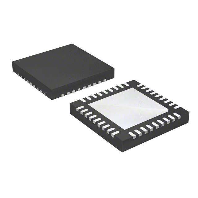
| 描述 | IC MIXER 300MHZ-2.5GHZ 40LFCSP |
| 产品分类 | |
| 品牌 | Analog Devices Inc |
| 数据手册 | |
| 产品图片 |
|
| 产品型号 | ADRF6601ACPZ-R7 |
| RF类型 | 手机 |
| rohs | 无铅 / 符合限制有害物质指令(RoHS)规范要求 |
| 产品系列 | - |
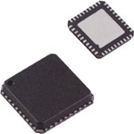
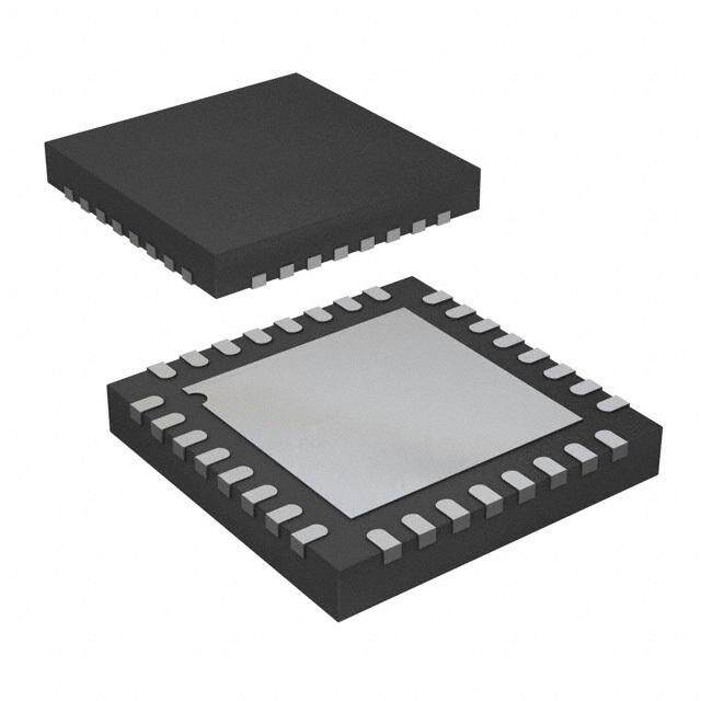
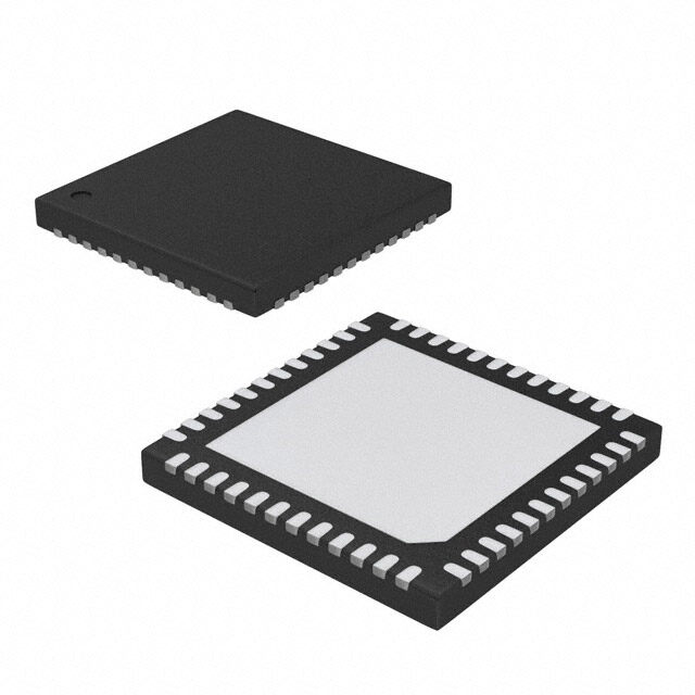
| 供应商器件封装 | 40-LFCSP-VQ(6x6) |
| 其它名称 | ADRF6601ACPZ-R7DKR |
| 包装 | Digi-Reel® |
| 噪声系数 | 14.8dB |
| 增益 | 6.7dB |
| 封装/外壳 | 40-VFQFN 裸露焊盘,CSP |
| 标准包装 | 1 |
| 混频器数 | 1 |
| 电压-电源 | 4.75 V ~ 5.25 V |
| 电流-电源 | - |
| 视频文件 | http://www.digikey.cn/classic/video.aspx?PlayerID=1364138032001&width=640&height=505&videoID=2245193150001http://www.digikey.cn/classic/video.aspx?PlayerID=1364138032001&width=640&height=505&videoID= 2474683260001 |
| 辅助属性 | 集成式 PLL 和 VCO |
| 频率 | 300MHz ~ 2.5GHz |


- 商务部:美国ITC正式对集成电路等产品启动337调查
- 曝三星4nm工艺存在良率问题 高通将骁龙8 Gen1或转产台积电
- 太阳诱电将投资9.5亿元在常州建新厂生产MLCC 预计2023年完工
- 英特尔发布欧洲新工厂建设计划 深化IDM 2.0 战略
- 台积电先进制程称霸业界 有大客户加持明年业绩稳了
- 达到5530亿美元!SIA预计今年全球半导体销售额将创下新高
- 英特尔拟将自动驾驶子公司Mobileye上市 估值或超500亿美元
- 三星加码芯片和SET,合并消费电子和移动部门,撤换高东真等 CEO
- 三星电子宣布重大人事变动 还合并消费电子和移动部门
- 海关总署:前11个月进口集成电路产品价值2.52万亿元 增长14.8%


PDF Datasheet 数据手册内容提取
300 MHz to 2500 MHz Rx Mixer with Integrated Fractional-N PLL and VCO Data Sheet ADRF6601 FEATURES The PLL can support input reference frequencies from 12 MHz to 160 MHz. The PFD output controls a charge pump whose Rx mixer with integrated fractional-N PLL output drives an off-chip loop filter. RF input frequency range: 300 MHz to 2500 MHz Internal LO frequency range: 750 MHz to 1160 MHz The loop filter output is then applied to an integrated VCO. The Input P1dB: 14.5 dBm VCO output at 2 × f is applied to an LO divider, as well as to a LO Input IP3: 31 dBm programmable PLL divider. The programmable PLL divider is IIP3 optimization via external pin controlled by a sigma-delta (Σ-Δ) modulator (SDM). The modulus SSB noise figure of the SDM can be programmed from 1 to 2047. IP3SET pin open: 13.5 dB The active mixer converts the single-ended 50 Ω RF input to IP3SET pin at 3.3 V: 14.6 dB a 200 Ω differential IF output. The IF output can operate up Voltage conversion gain: 6.7 dB to 500 MHz. Matched 200 Ω IF output impedance IF 3 dB bandwidth: 500 MHz The ADRF6601 is fabricated using an advanced silicon-germanium Programmable via 3-wire SPI interface BiCMOS process. It is available in a 40-lead, RoHS-compliant, 40-lead, 6 mm × 6 mm LFCSP 6 mm × 6 mm LFCSP with an exposed paddle. Performance is specified over the −40°C to +85°C temperature range. APPLICATIONS Table 1. Cellular base stations Internal LO ±3 dB RF ±1 dB RF IN IN GENERAL DESCRIPTION Part No. Range Balun Range Balun Range ADRF6601 750 MHz 300 MHz 450 MHz The ADRF6601 is a high dynamic range active mixer with an 1160 MHz 2500 MHz 1600 MHz integrated phase-locked loop (PLL) and a voltage controlled ADRF6602 1550 MHz 1000 MHz 1350 MHz oscillator (VCO). The PLL/synthesizer uses a fractional-N 2150 MHz 3100 MHz 2750 MHz PLL to generate a f input to the mixer. The reference input LO ADRF6603 2100 MHz 1100 MHz 1450 MHz can be divided or multiplied and then applied to the PLL phase 2600 MHz 3200 MHz 2850 MHz frequency detector (PFD). ADRF6604 2500 MHz 1200 MHz 1600 MHz 2900 MHz 3600 MHz 3200 MHz FUNCTIONAL BLOCK DIAGRAM VCC1 VCC2 VCC_LO VCC_MIX VCC_V2I VCC_LO NC NC 1 10 17 22 27 34 32 33 ADRF6601 LODRV_EN 36 INTERNAL LO RANGE LON 37 750MHz TO 1160MHz L3.D3OV 2 DECL3P3 BUFFER 2.5V LOP 38 LDO 9 DECL2P5 PLDLA_ETAN 1126 SPI FRARCETGION MODULUS INTREEGGER BUFFER M2U:1X 4,DB 2IYV, 1 VLDCOO 40 DECLVCO CLK 13 INTERFACE LE 14 THIRD-ORDER 26 RFIN FRACTIONAL INTERPOLATOR VCO ×2 N COUNTER PRESCALER CORE 29 IP3SET 21 TO 123 ÷2 REF_IN 6 ÷2 MUX CHARGE PUMP – PHASE 250µA, ÷4 TEMP + FREQUENCY 500µA (DEFAULT), SENSOR DETECTOR 750µA, MUXOUT 8 1000µA 4 7 11 15 20 21G2N3D24 25 28 30 31 35 RS5ET C3P VT3U9NE IF1P8 1IF9N 08546-001 Figure 1. Rev. B Document Feedback Information furnished by Analog Devices is believed to be accurate and reliable. However, no responsibility is assumed by Analog Devices for its use, nor for any infringements of patents or other One Technology Way, P.O. Box 9106, Norwood, MA 02062-9106, U.S.A. rights of third parties that may result from its use. Specifications subject to change without notice. No license is granted by implication or otherwise under any patent or patent rights of Analog Devices. Tel: 781.329.4700 ©2010–2014 Analog Devices, Inc. All rights reserved. Trademarks and registered trademarks are the property of their respective owners. Technical Support www.analog.com
ADRF6601 Data Sheet TABLE OF CONTENTS Features .............................................................................................. 1 Register 3—Σ-Δ Modulator Dither Control (Default: Applications ....................................................................................... 1 0x10000B) .................................................................................... 17 Register 4—PLL Charge Pump, PFD, and Reference Path General Description ......................................................................... 1 Control (Default: 0x0AA7E4) ................................................... 18 Functional Block Diagram .............................................................. 1 Register 5—PLL Enable and LO Path Control (Default: Revision History ............................................................................... 2 0x0000E5) .................................................................................... 19 Specifications ..................................................................................... 3 Register 6—VCO Control and VCO Enable (Default: RF Specifications .......................................................................... 3 0x1E2106) .................................................................................... 19 Synthesizer/PLL Specifications ................................................... 4 Register 7—Mixer Bias Enable and External VCO Enable Logic Input and Power Specifications ....................................... 4 (Default: 0x000007) .................................................................... 19 Timing Characteristics ................................................................ 5 Theory of Operation ...................................................................... 20 Absolute Maximum Ratings ............................................................ 6 Programming the ADRF6601 ................................................... 20 ESD Caution .................................................................................. 6 Initialization Sequence .............................................................. 20 Pin Configuration and Function Descriptions ............................. 7 LO Selection Logic ..................................................................... 21 Typical Performance Characteristics ............................................. 9 Applications Information .............................................................. 22 RF Frequency Sweep .................................................................... 9 Basic Connections for Operation ............................................. 22 IF Frequency Sweep ................................................................... 10 AC Test Fixture ............................................................................... 23 Spurious Performance................................................................ 15 Evaluation Board ............................................................................ 24 Register Structure ........................................................................... 16 Evaluation Board Control Software ......................................... 24 Register 0—Integer Divide Control (Default: 0x0001C0) .... 16 Schematic and Artwork ............................................................. 26 Register 1—Modulus Divide Control (Default: 0x003001) ........ 16 Evaluation Board Configuration Options ............................... 28 Register 2—Fractional Divide Control (Default: 0x001802) ...... 17 Outline Dimensions ....................................................................... 29 Ordering Guide .......................................................................... 29 REVISION HISTORY 1/14—Rev. A to Rev. B Replaced LO Range with RF Range in Data Sheet Title .............. 1 Updated Outline Dimensions ....................................................... 29 3/11—Rev. 0 to Rev. A Changes to Features Section, General Description Section, and Table 1 ............................................................................................ 1 Changes to Table 2 ............................................................................ 3 Changes to Conditions Statement and the Figure of Merit, Reference Spurs, and Phase Noise Parameters, Table 3; Changes to Conditions Statement and the Supply Current Parameter, Table 4 ........................................................................ 4 Changes to Table 6 ............................................................................ 6 Changes to Table 7 ............................................................................ 7 Replaced Typical Performance Characteristics Section .............. 9 Added Spurious Performance Section ......................................... 15 Changes to Figure 44 and Figure 45 ............................................. 19 Changes to Theory of Operation Section .................................... 20 Added AC Test Fixture Section and Figure 47; Renumbered Sequentially ......................................................... 23 Changes to Evaluation Board Control Software Section........... 24 Changes to Table 10 ........................................................................ 28 1/10—Revision 0: Initial Version Rev. B | Page 2 of 32
Data Sheet ADRF6601 SPECIFICATIONS RF SPECIFICATIONS V = 5 V, ambient temperature (T ) = 25°C, f = 153.6 MHz, f = 38.4 MHz, high-side LO injection, f = 140 MHz, IIP3 optimized S A REF PFD IF using CDAC = 0x0 and IP3SET = 3.3 V, unless otherwise noted. Table 2. Parameter Test Conditions/Comments Min Typ Max Unit INTERNAL LO FREQUENCY RANGE 750 1160 MHz RF INPUT FREQUENCY RANGE ±3 dB RF input range 300 2500 MHz RF INPUT AT 610 MHz Input Return Loss Relative to 50 Ω (can be improved with external match) −11.1 dB Input P1dB 14.8 dBm Second-Order Intercept (IIP2) −5 dBm each tone (10 MHz spacing between tones) 67.4 dBm Third-Order Intercept (IIP3) −5 dBm each tone (10 MHz spacing between tones) 33.4 dBm Single-Side Band Noise Figure IP3SET = 3.3 V 13.3 dB IP3SET = open 12.5 dB LO-to-IF Leakage At 1× LO frequency, 50 Ω termination at the RF port −55.5 dBm RF INPUT AT 910 MHz Input Return Loss Relative to 50 Ω (can be improved with external match) −16.7 dB Input P1dB 14.5 dBm Second-Order Intercept (IIP2) −5 dBm each tone (10 MHz spacing between tones) 55.3 dBm Third-Order Intercept (IIP3) −5 dBm each tone (10 MHz spacing between tones) 30.9 dBm Single-Side Band Noise Figure IP3SET = 3.3 V 14.6 dB IP3SET = open 13.5 dB LO-to-IF Leakage At 1× LO frequency, 50 Ω termination at the RF port −48 dBm RF INPUT AT 1020 MHz Input Return Loss Relative to 50 Ω (can be improved with external match) −16.8 dB Input P1dB 14.8 dBm Second-Order Intercept (IIP2) −5 dBm each tone (10 MHz spacing between tones) 60.9 dBm Third-Order Intercept (IIP3) −5 dBm each tone (10 MHz spacing between tones) 32.2 dBm Single-Side Band Noise Figure IP3SET = 3.3 V 14.8 dB IP3SET = open 13.5 dB LO-to-IF Leakage At 1× LO frequency, 50 Ω termination at the RF port −49 dBm IF OUTPUT Voltage Conversion Gain Differential 200 Ω load 6.7 dB IF Bandwidth Small signal 3 dB bandwidth 500 MHz Output Common-Mode Voltage External pull-up balun or inductors required 5 V Gain Flatness Over frequency range, any 5 MHz/50 MHz 0.2/0.5 dB Gain Variation Over full temperature range 1.2 dB Output Swing Differential 200 Ω load 2 V p-p Differential Output Return Loss Measured through 4:1 balun −15.5 dB LO INPUT/OUTPUT (LOP, LON) Externally applied 1× LO input, internal PLL disabled Frequency Range 250 6000 MHz Output Level (LO as Output) 1× LO into a 50 Ω load, LO output buffer enabled −6 dBm Input Level (LO as Input) −6 0 +6 dBm Input Impedance 50 Ω Rev. B | Page 3 of 32
ADRF6601 Data Sheet SYNTHESIZER/PLL SPECIFICATIONS V = 5 V, ambient temperature (T ) = 25°C, f = 153.6 MHz, f power = 4 dBm, f = 38.4 MHz, high-side LO injection, S A REF REF PFD f = 140 MHz, IIP3 optimized using CDAC = 0x0 and IP3SET = 3.3 V, unless otherwise noted. IF Table 3. Parameter Test Conditions/Comments Min Typ Max Unit SYNTHESIZER SPECIFICATIONS Synthesizer specifications referenced to 1× LO Frequency Range Internally generated LO 750 1160 MHz Figure of Merit1 P = 0 dBm −222 dBc/Hz/Hz REF_IN Reference Spurs f = 38.4 MHz PFD f /4 −107 dBc PFD f −83 dBc PFD >f −88 dBc PFD PHASE NOISE f = 750 MHz to 1160 MHz, f = 38.4 MHz LO PFD 1 kHz to 10 kHz offset −99 dBc/Hz 100 kHz offset −108 dBc/Hz 500 kHz offset −127 dBc/Hz 1 MHz offset −135 dBc/Hz 5 MHz offset −147 dBc/Hz 10 MHz offset −151 dBc/Hz 20 MHz offset −153 dBc/Hz Integrated Phase Noise 1 kHz to 40 MHz integration bandwidth 0.14 °rms PFD Frequency 20 40 MHz REFERENCE CHARACTERISTICS REF_IN, MUXOUT pins REF_IN Input Frequency 12 160 MHz REF_IN Input Capacitance 4 pF MUXOUT Output Level V (lock detect output selected) 0.25 V OL V (lock detect output selected) 2.7 V OH MUXOUT Duty Cycle 50 % CHARGE PUMP Pump Current Programmable to 250 µA, 500 µA, 750 µA, 1 mA 500 µA Output Compliance Range 1 2.8 V 1 The figure of merit (FOM) is computed as phase noise (dBc/Hz) – 10 log 10(fPFD) – 20 log 10(fLO/fPFD). The FOM was measured across the full LO range with fREF = 80 MHz, and fREF power = 10 dBm (500 V/µs slew rate) with a 40 MHz fPFD. The FOM was computed at 50 kHz offset. LOGIC INPUT AND POWER SPECIFICATIONS V = 5 V, ambient temperature (T ) = 25°C, f = 153.6 MHz, f = 38.4 MHz, high-side LO injection, f = 140 MHz, IIP3 optimized S A REF PFD IF using CDAC = 0x0 and IP3SET = 3.3 V, unless otherwise noted. Table 4. Parameter Test Conditions/Comments Min Typ Max Unit LOGIC INPUTS CLK, DATA, LE Input High Voltage, V 1.4 3.3 V INH Input Low Voltage, V 0 0.7 V INL Input Current, I /I 0.1 µA INH INL Input Capacitance, C 5 pF IN POWER SUPPLIES VCC1, VCC2, VCC_LO, VCC_MIX, and VCC_V2I pins Voltage Range 4.75 5 5.25 V Supply Current PLL only 97 mA External LO mode (internal PLL disabled, IP3SET pin = 3.3 V, LO output buffer off) 184 mA Internal LO mode (internal PLL enabled, IP3SET pin = 3.3 V, LO output buffer on) 294 mA Internal LO mode (internal PLL enabled, IP3SET pin = 3.3 V, LO output buffer off) 281 mA Power-down mode 30 mA Rev. B | Page 4 of 32
Data Sheet ADRF6601 TIMING CHARACTERISTICS V = 5 V ± 5%. S Table 5. Parameter Limit Unit Description t 20 ns min LE setup time 1 t 10 ns min DATA-to-CLK setup time 2 t 10 ns min DATA-to-CLK hold time 3 t 25 ns min CLK high duration 4 t 25 ns min CLK low duration 5 t 10 ns min CLK-to-LE setup time 6 t 20 ns min LE pulse width 7 Timing Diagram t4 t5 CLK t2 t3 DB2 DB1 DB0(LSB) DATA DB23(MSB) DB22 (CONTROLBITC3) (CONTROLBITC2) (CONTROLBITC1) t1 t6 t7 LE 08546-002 Figure 2. Timing Diagram Rev. B | Page 5 of 32
ADRF6601 Data Sheet ABSOLUTE MAXIMUM RATINGS Table 6. Stresses above those listed under Absolute Maximum Ratings Parameter Rating may cause permanent damage to the device. This is a stress Supply Voltage, VCC1, VCC2, VCC_LO, −0.5 V to +5.5 V VCC_MIX, VCC_V2I rating only; functional operation of the device at these or any Digital I/O, CLK, DATA, LE, LODRV_EN, −0.3 V to +3.6 V other conditions above those indicated in the operational PLL_EN section of this specification is not implied. Exposure to absolute VTUNE 0 V to 3.3 V maximum rating conditions for extended periods may affect IFP, IFN −0.3 V to VCC_V2I + 0.3 V device reliability. RFIN 16 dBm LOP, LON, REF_IN 13 dBm ESD CAUTION θ (Exposed Paddle Soldered Down) 35°C/W JA Maximum Junction Temperature 150°C Operating Temperature Range −40°C to +85°C Storage Temperature Range −65°C to +150°C Rev. B | Page 6 of 32
Data Sheet ADRF6601 PIN CONFIGURATION AND FUNCTION DESCRIPTIONS N O E C _ O VLCEDENUTVPOLNOLVRDOLDNGL_CCVCNCNDNG 0987654321 4333333333 VCC1 1 PIN 1 30GND DECL3P3 2 INDICATOR 29IP3SET CP 3 28GND GND 4 27VCC_V2I RSET 5 ADRF6601 26RFIN REF_IN 6 TOP VIEW 25GND GND 7 (Not to Scale) 24GND MUXOUT 8 23GND DECL2P5 9 22VCC_MIX VCC210 21GND 11213141516171819102 DAKEDNOPND NGTADLCLNGE_LL_CFIFING LPCV NOTES 12 .. NTLHOCE W= E NIXMOPP OCEOSDENADNNECPCAE DTG.D RDLOOEU NSNOHDOT P UCLLOADNN BNEEE. CSTO TLHDIESR PEIDN.TO A 08546-003 Figure 3. Pin Configuration Table 7. Pin Function Descriptions Pin No. Mnemonic Description 1 VCC1 Power Supply for the 3.3 V LDO. Power supply voltage range is 4.75 V to 5.25 V. Each power supply pin should be decoupled with a 100 pF capacitor and a 0.1 µF capacitor located close to the pin. 2 DECL3P3 Decoupling Node for the 3.3 V LDO. Connect a 0.1 µF capacitor between this pin and ground. 3 CP Charge Pump Output Pin. Connect to VTUNE through the loop filter. 4, 7, 11, 15, 20, GND Ground. Connect these pins to a low impedance ground plane. 21, 23, 24, 25, 28, 30, 31, 35 5 R Charge Pump Current. The nominal charge pump current can be set to 250 µA, 500 µA, 750 µA, or 1 mA using SET Bit DB11 and Bit DB10 in Register 4 and by setting Bit DB18 in Register 4 to 0 (internal reference current). In this mode, no external R is required. If Bit DB18 is set to 1, the four nominal charge pump currents (I ) SET NOMINAL can be externally adjusted according to the following equation: 217.4 × I R = CP −37.8Ω SET I NOMINAL 6 REF_IN Reference Input. Nominal input level is 1 V p-p. Input range is 12 MHz to 160 MHz. This pin is internally dc- biased and should be ac-coupled. 8 MUXOUT Multiplexer Output. This output can be programmed to provide the reference output signal or the lock detect signal. The output is selected by programming the appropriate register. 9 DECL2P5 Decoupling Node for the 2.5 V LDO. Connect a 0.1 µF capacitor between this pin and ground. 10 VCC2 Power Supply for the 2.5 V LDO. Power supply voltage range is 4.75 V to 5.25 V. Each power supply pin should be decoupled with a 100 pF capacitor and a 0.1 µF capacitor located close to the pin. 12 DATA Serial Data Input. The serial data input is loaded MSB first; the three LSBs are the control bits. 13 CLK Serial Clock Input. The serial clock input is used to clock in the serial data to the registers. The data is latched into the 24-bit shift register on the CLK rising edge. Maximum clock frequency is 20 MHz. 14 LE Load Enable. When the LE input pin goes high, the data stored in the shift registers is loaded into one of the eight registers. The relevant latch is selected by the three control bits of the 24-bit word. 16 PLL_EN PLL Enable. Switch between internal PLL and external LO input. When this pin is logic high, the mixer LO is automatically switched to the internal PLL and the internal PLL is powered up. When this pin is logic low, the internal PLL is powered down and the external LO input is routed to the mixer LO inputs. The SPI can also be used to switch modes. 17, 34 VCC_LO Power Supply. Power supply voltage range is 4.75 V to 5.25 V. Each power supply pin should be decoupled with a 100 pF capacitor and a 0.1 µF capacitor located close to the pin. 18, 19 IFP, IFN Mixer IF Outputs. These outputs should be pulled to VCC with RF chokes. Rev. B | Page 7 of 32
ADRF6601 Data Sheet Pin No. Mnemonic Description 22 VCC_MIX Power Supply. Power supply voltage range is 4.75 V to 5.25 V. Each power supply pin should be decoupled with a 100 pF capacitor and a 0.1 µF capacitor located close to the pin. 26 RF RF Input (single-ended, 50 Ω). IN 27 VCC_V2I Power Supply. Power supply voltage range is 4.75 V to 5.25 V. Each power supply pin should be decoupled with a 100 pF capacitor and a 0.1 µF capacitor located close to the pin. 29 IP3SET Connect a resistor from this pin to a 5 V supply to adjust IIP3. Normally leave open. 32, 33 NC No Connection. 36 LODRV_EN LO Driver Enable. Together with Pin 16 (PLL_EN), this digital input pin determines whether the LOP and LON pins operate as inputs or outputs. LOP and LON become inputs if the PLL_EN pin is low or if the PLL_EN pin is set high if the PLEN bit (DB6 in Register 5) is set to 0. LOP and LON become outputs if either the LODRV_EN pin or the LDRV bit (DB3 in Register 5) is set to 1 while the PLL_EN pin is set high. The external LO drive frequency must be 1× LO. This pin has an internal 100 kΩ pull-down resistor. 37, 38 LON, LOP Local Oscillator Input/Output. The internally generated 1× LO is available on these pins. When internal LO generation is disabled, an external 1× LO can be applied to these pins. 39 VTUNE VCO Control Voltage Input. This pin is driven by the output of the loop filter. The nominal input voltage range on this pin is 1.5 V to 2.5 V. 40 DECLVCO Decoupling Node for the VCO LDO. Connect a 100 pF capacitor and a 10 µF capacitor between this pin and ground. EPAD Exposed Paddle. The exposed paddle should be soldered to a low impedance ground plane. Rev. B | Page 8 of 32
Data Sheet ADRF6601 TYPICAL PERFORMANCE CHARACTERISTICS RF FREQUENCY SWEEP CDAC = 0x0, internally generated high-side LO, RF = −5 dBm, f = 140 MHz, unless otherwise noted. IN IF 5 45 4 IIPP33SSEETT == 3O.P3VEN TTAA == ++2855°°CC 40 IIPP33SSEETT == O3.P3VEN TA = –40°C 3 35 2 m) 30 B) 1 dB N (d 0 P3 ( 25 AI T I G –1 NPU 20 –2 I TA = +85°C 15 TA = +25°C –3 TA = –40°C 10 –4 –5610 660 710 R7F6 F0REQ8U1E0NCY8 (6M0Hz) 910 960 1010 08546-004 5610 660 710 R7F6 F0REQ8U1E0NCY8 (6M0Hz) 910 960 1010 08546-007 Figure 4. Gain vs. RF Frequency Figure 7. Input IP3 vs. RF Frequency 90 20 IP3SET = OPEN TA = +85°C IP3SET = OPEN IP3SET = 3.3V TA = +25°C 18 IP3SET = 3.3V 80 TA = –40°C 16 14 m) 70 Bm) B d 12 INPUT IP2 (d 6500 INPUT P1dB ( 1086 TTTAAA === –++428055°°°CCC 4 40 2 30610 660 710 R7F6 0FREQ8U1E0NCY8 (6M0Hz) 910 960 1010 08546-005 0610 660 710 R7F6 F0REQ8U1E0NCY8 (6M0Hz) 910 960 1010 08546-008 Figure 5. Input IP2 vs. RF Frequency Figure 8. Input P1dB vs. RF Frequency 20 IP3SET = OPEN 18 IP3SET = 3.3V 16 B) 14 d E ( 12 R U G 10 FI E S 8 NOI 6 TTAA == ++2855°°CC TA = –40°C 4 2 0610 660 710 R7F6 F0REQ8U1E0NCY8 (6M0Hz) 910 960 1010 08546-006 Figure 6. Noise Figure vs. RF Frequency Rev. B | Page 9 of 32
ADRF6601 Data Sheet IF FREQUENCY SWEEP CDAC = 0x0, internally generated swept low-side LO, f = 1960 MHz, RF = −5 dBm, unless otherwise noted. RF IN 5 45 IP3SET = OPEN TA = +85°C IP3SET = OPEN 4 IP3SET = 3.3V TTAA == –+4205°°CC 40 IP3SET = 3.3V 3 35 2 m) 30 B) 1 dB N (d 0 P3 ( 25 AI T I G –1 NPU 20 –2 I TA = +85°C 15 TA = +25°C –3 TA = –40°C 10 –4 –5 5 25 50 75 10012515IF0 F1R75EQ20U0E2N2C5Y2 (5M0H2z7)5300325350375400 08546-009 25 50 75 10012515IF0 F1R75EQ20U0E2N2C5Y2 (5M0H2z7)5300325350375400 08546-012 Figure 9. Gain vs. IF Frequency Figure 12. Input IP3 vs. IF Frequency, RFIN = −5 dBm 90 20 IP3SET = OPEN TA = +85°C IP3SET = OPEN IP3SET = 3.3V TA = +25°C 18 IP3SET = 3.3V 80 TA = –40°C 16 14 m) 70 m) PUT IP2 (dB 60 UT P1dB (dB 11208 IN 50 NP TA = +85°C I 6 TA = +25°C TA = –40°C 4 40 2 3025 50 75 10012515IF0 F1R75EQ20U0E2N2C5Y2 (5M0H2z7)5300325350375400 08546-010 025 50 75 10012515IF0 F1R75EQ20U0E2N2C5Y2 (5M0H2z7)5300325350375400 08546-013 Figure 10. Input IP2 vs. IF Frequency, RFIN = −5 dBm Figure 13. Input P1dB vs. IF Frequency 20 IP3SET = OPEN 18 IP3SET = 3.3V 16 B) 14 d E ( 12 R U G 10 FI SE 8 NOI 6 TTAA == ++2855°°CC 4 TA = –40°C 2 0 25 50 75 10012515IF0 F1R75EQ20U0E2N2C5Y2 (5M0H2z7)5300325350375400 08546-011 Figure 11. Noise Figure vs. IF Frequency Rev. B | Page 10 of 32
Data Sheet ADRF6601 0 0 –5 IP3SET = OPEN TA = +85°C –10 IP3SET = 3.3V TTAA == –+4205°°CC –5 m) –15 B –10 ROUGH (d –––322050 SS (dB) –15 TH –35 LO –20 D N F FEE ––4450 ETUR –25 O-I –50 R O-T –55 –30 L –60 –35 –65 –70 –40 750 800 850 L9O0 0FREQ9U5E0NCY1 0(M00Hz)1050 1100 1150 08546-014 500 600 700 LO80 F0REQU90E0NCY 1(0M0H0z) 1100 1200 1300 08546-017 Figure 14. LO-to-IF Feedthrough vs. LO Frequency, Figure 17. LO Input Return Loss vs. LO Frequency (Including TC1-1-13 Balun) LO Output Turned Off, CDAC = 0x0 –30 350 3.5 IP3SET = OPEN TA = +85°C –40 IP3SET = 3.3V TTAA == –+4205°°CC 300 3.0 RESISTANCE m) 250 2.5 dB –50 Ω) pF) GE ( CE ( 200 2.0 CE ( A N N K –60 A A F LEA ESIST 150 CAPACITANCE 1.5 PACIT LO-R –70 R 100 1.0 CA –80 50 0.5 –90 0 0 750 800 850 L9O0 0FREQ9U5E0NCY1 0(M00Hz)1050 1100 1150 08546-015 50 100 150 20IF0 FRE25Q0UEN3C0Y0 (MH3z5)0 400 450 500 08546-018 Figure 15. LO-to-RF Leakage vs. LO Frequency, LO Output Turned Off Figure 18. IF Differential Output Impedance (R Parallel C Equivalent) 0 35 IP3SET = OPEN –5 IP3SET = 3.3V 30 –10 B) B) SS (d –15 RE (d 25 ETURN LO ––2250 OISE FIGU 20 R N –30 15 –35 –40500 600 700 RF8 0F0REQU90E0NCY 1(0M0H0z) 1100 1200 1300 08546-016 10–60 –50 CW–4 0B LOCKE–R30 L EVEL (–d2B0 m) –10 0 08546-019 Figure 16. RF Input Return Loss vs. RF Frequency Figure 19. SSB Noise Figure vs. 5 MHz Offset Blocker Level, LO Frequency = 1055 MHz, RF Frequency = 915 MHz Rev. B | Page 11 of 32
ADRF6601 Data Sheet 0 5.0 ––11–505 IIPP33SSEETT == 3O.P3VEN TTTAAA === ++–428055°°°CCC 44..50 TTTAAA === –++428055°°°CCC c) ON (dB ––2250 GE (V) 33..50 TI –30 A A T OL –35 OL 2.5 F-TO-IF IS –––544050 VTUNE V 21..05 R –55 1.0 –60 0.5 –65 –70 0 550 650 750 RF8 5F0REQU95E0NCY 1(M05H0z) 1150 1250 1350 08546-020 750 800 850 L9O0 0FREQ9U5E0NCY1 0(0M0Hz)1050 1100 1150 08546-023 Figure 20. RF-to-IF Isolation vs. RF Frequency, High-Side LO, IF = 140 MHz, Figure 23. VTUNE vs. LO Frequency LO Output Turned Off 0 350 –1 IIPP33SSEETT == 3O.P3VEN TTAA == ++2855°°CC IIPP33SSEETT == 3O.P3VEN TA = –40°C m) –2 300 B E (d –3 mA) MPLITUD ––45 URRENT ( 250 A C O OUTPUT ––67 SUPPLY 200 TTTAAA === ++–428055°°°CCC L –8 150 –9 –10 100 750 800 850 L9O0 0FREQ9U5E0NCY1 0(M00Hz)1050 1100 1150 08546-021 750 800 850 L9O0 0FREQ9U5E0NCY1 0(M00Hz)1050 1100 1150 08546-024 Figure 21. LO Output Amplitude vs. LO Frequency Figure 24. Supply Current vs. LO Frequency 20 2.0 MHz) 15 1.9 IIPP33SSEETT == 3O.P3VEN Hz ( 1.8 0M 10 ROM 92 5 GE (V) 11..67 F A ON 0 OLT 1.5 TI V VIA –5 AT 1.4 Y DE VPT 1.3 C –10 EN 1.2 U Q –15 E 1.1 R F –200 50 100TIME (µs)150 200 250 08546-022 1.0–55 –35 –15 TE5MPERA25TURE (4°5C) 65 85 105 08546-025 Figure 22. Frequency Deviation from 910 MHz vs. Time Figure 25. VPTAT Voltage vs. Temperature (IP3SET = Optimized, Open) (Demonstrates LO Frequency Settling Time from 920 MHz to 910 MHz) Rev. B | Page 12 of 32
Data Sheet ADRF6601 Complementary cumulative distribution function (CCDF), f = 2140 MHz, f = 140 MHz. RF IF 100 100 IP3SET = OPEN IP3SET = OPEN 90 IP3SET = 3.3V 90 IP3SET = 3.3V %) 80 %) 80 E ( E ( AG 70 AG 70 T T N N E 60 E 60 C C R R N PE 50 TTAA == ++2855°°CC N PE 50 O 40 TA = –40°C O 40 TI TI U U RIB 30 RIB 30 T T DIS 20 DIS 20 TA = +85°C 10 10 TTAA == –+4205°°CC 0 0 –2.0 –1.5 –1.0 –0.5 0GAI0N.5 (dB)1.0 1.5 2.0 2.5 3.0 08546-026 24 26 28 3I0NPUT I3P23 (dBm3)4 36 38 40 08546-029 Figure 26. Gain Figure 29. Input IP3 100 100 IP3SET = OPEN IP3SET = OPEN 90 IP3SET = 3.3V 90 IP3SET = 3.3V DISTRIBUTION PERCENTAGE (%) 23456780000000 TTTAAA === –++428055°°°CCC DISTRIBUTION PERCENTAGE (%) 23456780000000 TA = +85°C 10 10 TTAA == –+4205°°CC 050 55 60 INPUT I6P52 (dBm)70 75 80 08546-027 010 11 12 I1N3PUT P114dB (dB1m5) 16 17 18 08546-030 Figure 27. Input IP2 Figure 30. Input P1dB 100 100 IP3SET = OPEN IP3SET = OPEN 90 90 IP3SET = 3.3V DISTRIBUTION PERCENTAGE (%) 23456780000000 TA = +85°C DISTRIBUTION PERCENTAGE (%) 23456780000000 TTTAAA === –++428055°°°CCC 10 TTAA == +–4205°°CC 10 09 10 11 N1O2ISE FI1G3URE (1d4B) 15 16 17 08546-028 0–90 –80 L–O7 0FEEDTH–R6O0UGH (d–B5m0) –40 –30 08546-031 Figure 28. Noise Figure Figure 31. LO Feedthrough to IF, LO Output Turned Off Rev. B | Page 13 of 32
ADRF6601 Data Sheet Measured at IF output, CDAC = 0x0, IP3SET = open, internally generated high-side LO, f = 153.6 MHz, f = 38.4 MHz, REF PFD RF = −5 dBm, f = 140 MHz, unless otherwise noted. Phase noise measurements made at LO output, unless otherwise noted. IN IF –80 0.50 –90 LO FREQUENCY = 1155.2MHz TTTAAA === –++428055°°°CCC ms) 00..4450 TTTAAA === ++–428055°°°CCC Hz) –100 SE (°r 0.35 E (dBc/ –110 SE NOI 0.30 S –120 A 0.25 OI H PHASE N ––114300 LO FREQUENCY = 752MHz GRATED P 00..2105 E T 0.10 N –150 I 0.05 –160 0 1k 10k OFFS1E00Tk FREQUEN1MCY (Hz) 10M 100M 08546-032 750 800 850 L9O0 0FREQ9U5E0NCY1 0(0M0Hz)1050 1100 1150 08546-035 Figure 32. Phase Noise vs. Offset Frequency Figure 35. Integrated Phase Noise vs. LO Frequency –75 –90 OFFSET AT 2× PFD FREQUENCY OFFSET AT 4× PFD FREQUENCY OFFSET = 1kHz –80 –100 TA = +85°C c) –85 TTAA == +–4205°°CC Hz) –110 dB Bc/ RS LEVEL ( ––9950 E NOISE (d ––112300 OFFSET = 100kHz TTTAAA === –++428055°°°CCC U S P A S –100 PH –140 OFFSET = 5MHz –105 –150 –110 –160 750 800 850 L9O0 0FREQ9U50ENCY1 0(0M0Hz)1050 1100 1150 08546-033 750 800 850 L9O0 0FREQ9U5E0NCY1 0(M00Hz)1050 1100 1150 08546-036 Figure 33. PLL Reference Spurs vs. LO Frequency (2× PFD and 4× PFD) Figure 36. Phase Noise vs. LO Frequency (1 kHz, 100 kHz, and 5 MHz Steps) –75 –100 OFFSET AT 3× PFD FREQUENCY OFFSET AT 1× PFD FREQUENCY TA = +85°C –105 –80 TTAA == –+4205°°CC –110 OFFSET = 10kHz Bc) –85 c/Hz) –115 EL (d –90 E (dB –120 RS LEV –95 E NOIS ––112350 OFFSET = 1MHz U S P A S –100 PH –135 –140 TA = +85°C –105 0F.R2E5×Q PUFEDNCY –145 TTAA == –+4205°°CC –110750 800 850 L9O0 0FREQ9U5E0NCY1 0(M00Hz)1050 1100 1150 08546-034 –150750 800 850 L9O0 0FREQ9U5E0NCY1 0(M00Hz)1050 1100 1150 08546-037 Figure 34. PLL Reference Spurs vs. LO Frequency (0.25× PFD, 1× PFD, and 3× PFD) Figure 37. Phase Noise vs. LO Frequency (10 kHz, 1 MHz Steps) Rev. B | Page 14 of 32
Data Sheet ADRF6601 SPURIOUS PERFORMANCE (N × f ) − (M × f ) spur measurements were made using the standard evaluation board (see the Evaluation Board section). Mixer spurious RF LO products were measured in dB relative to the carrier (dBc) from the IF output power level. All spurious components greater than −125 dBc are shown. LO = 750 MHz, RF = 610 MHz (horizontal axis is m, vertical axis is n), and RF power = 0 dBm. IN M 0 1 2 3 4 0 −115.74 −63.28 −31.83 −54.52 −33.54 1 −49.49 0.0 −64.58 −24.09 −71.52 2 −48.77 −42.49 −75.23 −60.35 −67.88 N 3 −81.30 −71.27 −103.32 −73.13 −110.05 4 −83.02 −91.24 −105.20 −88.27 −113.66 5 −103.16 −111.19 −114.25 −108.4 −115.31 6 −110.88 −112.83 −112.85 −113.85 −113.55 7 −110.87 −108.26 −112.91 −111.93 −113.64 LO = 1050 MHz, RF = 910 MHz (horizontal axis is m, vertical axis is n), and RF power = 0 dBm. IN M 0 1 2 3 4 0 −113.23 −57.96 −27.78 −58.01 −40.34 1 −34.12 0.0 −58.72 −27.14 −84.94 2 −49.76 −47.19 −57.30 −68.48 −65.03 N 3 −73.54 −74.12 −102.24 −72.99 −108.62 4 −102.66 −110.29 −100.07 −99.75 −112.69 5 −108.79 −107.57 −110.94 −110.16 −115.35 6 −110.79 −108.34 −107.38 −112.44 −113.78 7 −109.87 −109.71 −108.58 −110.01 Rev. B | Page 15 of 32
ADRF6601 Data Sheet REGISTER STRUCTURE This section provides the register maps for the ADRF6601. The three LSBs determine the register that is programmed. REGISTER 0—INTEGER DIVIDE CONTROL (DEFAULT: 0x0001C0) DIVIDE RESERVED MODE INTEGER DIVIDE RATIO CONTROL BITS DB23 DB22 DB21 DB20 DB19 DB18 DB17 DB16 DB15 DB14 DB13 DB12 DB11 DB10 DB9 DB8 DB7 DB6 DB5 DB4 DB3 DB2 DB1 DB0 0 0 0 0 0 0 0 0 0 0 0 0 0 DM ID6 ID5 ID4 ID3 ID2 ID1 ID0 C3(0) C2(0) C1(0) DM DIVIDE MODE 0 FRACTIONAL (DEFAULT) 1 INTEGER ID6 ID5 ID4 ID3 ID2 ID1 ID0 INTEGER DIVIDE RATIO 0 0 1 0 1 0 1 21 (INTEGER MODE ONLY) 0 0 1 0 1 1 0 22 (INTEGER MODE ONLY) 0 0 1 0 1 1 1 23 (INTEGER MODE ONLY) 0 0 1 1 0 0 0 24 ... ... ... ... ... ... ... ... ... ... ... ... ... ... ... ... 0 1 1 1 0 0 0 56 (DEFAULT) ... ... ... ... ... ... ... ... ... ... ... ... ... ... ... ... 1 1 1 0 1 1 1 119 1 1 1 1 0 0 0 120 (INTEGER MODE ONLY) 1 1 1 1 0 0 1 121 (INTEGER MODE ONLY) 11 11 11 11 00 11 01 112223 ((IINNTTEEGGEERR MMOODDEE OONNLLYY)) 08546-038 Figure 38. Register 0—Integer Divide Control Register Map REGISTER 1—MODULUS DIVIDE CONTROL (DEFAULT: 0x003001) RESERVED MODULUS VALUE CONTROL BITS DB23 DB22 DB21 DB20 DB19 DB18 DB17 DB16 DB15 DB14 DB13 DB12 DB11 DB10 DB9 DB8 DB7 DB6 DB5 DB4 DB3 DB2 DB1 DB0 0 0 0 0 0 0 0 0 0 0 MD10 MD9 MD8 MD7 MD6 MD5 MD4 MD3 MD2 MD1 MD0 C3(0) C2(0) C1(1) MD10 MD9 MD8 MD7 MD6 MD5 MD4 MD3 MD2 MD1 MD0 MODULUS VALUE 0 0 0 0 0 0 0 0 0 0 1 1 0 0 0 0 0 0 0 0 0 1 0 2 ... ... ... ... ... ... ... ... ... ... ... ... ... ... ... ... ... ... ... ... ... ... ... ... 1 1 0 0 0 0 0 0 0 0 0 1536 (DEFAULT) ... ... ... ... ... ... ... ... ... ... ... ... .1.. .1.. .1.. .1.. .1.. .1.. .1.. .1.. .1.. .1.. .1.. .2.0.47 08546-039 Figure 39. Register 1—Modulus Divide Control Register Map Rev. B | Page 16 of 32
Data Sheet ADRF6601 REGISTER 2—FRACTIONAL DIVIDE CONTROL (DEFAULT: 0x001802) RESERVED FRACTIONAL VALUE CONTROL BITS DB23 DB22 DB21 DB20 DB19 DB18 DB17 DB16 DB15 DB14 DB13 DB12 DB11 DB10 DB9 DB8 DB7 DB6 DB5 DB4 DB3 DB2 DB1 DB0 0 0 0 0 0 0 0 0 0 0 FD10 FD9 FD8 FD7 FD6 FD5 FD4 FD3 FD2 FD1 FD0 C3(0) C2(1) C1(0) FD10 FD9 FD8 FD7 FD6 FD5 FD4 FD3 FD2 FD1 FD0 FRACTIONAL VALUE 0 0 0 0 0 0 0 0 0 0 0 0 0 0 0 0 0 0 0 0 0 0 1 1 ... ... ... ... ... ... ... ... ... ... ... ... ... ... ... ... ... ... ... ... ... ... ... ... 0 1 1 0 0 0 0 0 0 0 0 768 (DEFAULT) ... ... ... ... ... ... ... ... ... ... ... ... ... ... FRA...CTION.A..L VAL.U..E MUS..T. BE L.E..SS TH.A..N MOD..U.LUS... ... .<.M. DR 08546-040 Figure 40. Register 2—Fractional Divide Control Register Map REGISTER 3—Σ-Δ MODULATOR DITHER CONTROL (DEFAULT: 0x10000B) DITHER DITHER MAGNITUDE ENABLE DITHER RESTART VALUE CONTROL BITS DB23 DB22 DB21 DB20 DB19DB18DB17DB16DB15DB14DB13DB12DB11DB10 DB9 DB8 DB7 DB6 DB5 DB4 DB3 DB2 DB1 DB0 0 DITH1 DITH0 DEN DV16DV15DV14DV13DV12DV11DV10 DV9 DV8 DV7 DV6 DV5 DV4 DV3 DV2 DV1 DV0 C3(0)C2(1)C1(1) DITH1 DITH0 DITHER MAGNITUDE 0 0 15 (DEFAULT) 0 1 7 1 0 3 1 1 1 (RECOMMENDED) DEN DITHER ENABLE 0 DISABLE 1 ENABLE (DEFAULT, RECOMMENDED) DITHER RESTART DV16DV15DV14DV13DV12DV11DV10 DV9 DV8 DV7 DV6 DV5 DV4 DV3 DV2 DV1 DV0 VALUE 0 0 0 0 0 0 0 0 0 0 0 0 0 0 0 0 1 0x00001 (DEFAULT) ... ... ... ... ... ... ... ... ... ... ... ... ... ... ... ... ... ... 1... 1... 1... 1... 1... 1... 1... 1... 1... 1... 1... 1... 1... 1... 1... 1... 1... .0.x.1FFFF 08546-041 Figure 41. Register 3—Σ-Δ Modulator Dither Control Register Map Rev. B | Page 17 of 32
ADRF6601 Data Sheet REGISTER 4—PLL CHARGE PUMP, PFD, AND REFERENCE PATH CONTROL (DEFAULT: 0x0AA7E4) MRUEXF SOEULPEUCTT INPPUATT HREF CSUORRCUREPREFCNET PPOFDL PFDM PUHLATSIEP LOIEFRFSET CURCRPENT SCRPC CONCTPROL PFD EDGE BPAFDCDEK LALAANYSTHI CONTROL BITS DB23 DB22 DB21 DB20 DB19 DB18 DB17 DB16 DB15 DB14 DB13 DB12 DB11 DB10 DB9 DB8 DB7 DB6 DB5 DB4 DB3 DB2 DB1 DB0 RMS2 RMS1 RMS0 RS1 RS0 CPM CPBD CPB4 CPB3 CPB2 CPB1 CPB0 CPP1 CPP0 CPS CPC1 CPC0 PE1 PE0 PAB1 PAB0 C3(1) C2(0) C1(0) PAB0 PAB1 PFD ANTI BACKLASH DELAY 0 0 0ns (DEFAULT) 0 1 0.5ns 1 0 0.75ns 1 1 0.9ns REFERENCE PATH EDGE PE0 SENSITIVITY 0 FALLING EDGE 1 RISING EDGE (DEFAULT) DIVIDER PATH EDGE PE1 SENSITIVITY 0 FALLING EDGE 1 RISING EDGE (DEFAULT) CPC1CPC0 CHARGE PUMP CONTROL 0 0 BOTH ON 0 1 PUMP DOWN 1 0 PUMP UP 1 1 TRISTATE (DEFAULT) CPS CHARGE PUMP CONTROL SOURCE 0 CONTROL BASED ON STATE OF DB7/DB8 (CP CONTROL) 1 CONTROL FROM PFD (DEFAULT) CPP1 CPP0 CHARGE PUMP CURRENT 0 0 250µA 0 1 500µA (DEFAULT) 1 0 750µA 1 1 1000µA CPB4 CPB3 CPB2 CPB1 CPB0 PFD PHASE OFFSET MULTIPLIER 0 0 0 0 0 0 × 22.5°/ICPMULT 0 0 0 0 1 1 × 22.5°/ICPMULT 0 0 1 1 0 6 × 22.5°/ICPMULT (RECOMMENDED) 0 1 0 1 0 10 × 22.5°/ICPMULT (DEFAULT) 1 0 0 0 0 16 × 22.5°/ICPMULT 1 1 1 1 1 31 × 22.5°/ICPMULT CPBD PFD PHASE OFFSET POLARITY 0 NEGATIVE 1 POSITIVE (DEFAULT) CPM CHARGE PUMP CURRENT REFERENCE SOURCE 0 INTERNAL (DEFAULT) 1 EXTERNAL INPUT REFERENCE RS0 RS1 PATH SOURCE 0 0 2× REF_IN 0 1 REF_IN (DEFAULT) 1 0 0.5× REF_IN 1 1 0.25× REF_IN RMS2 RMS1 RMS0 REF OUTPUT MUX SELECT 0 0 0 LOCK DETECT (DEFAULT) 0 0 1 VPTAT 0 1 0 REF_IN (BUFFERED) 0 1 1 0.5× REF_IN (BUFFERED) 1 0 0 2× REF_IN (BUFFERED) 111 011 101 TRRREEISSSEETRRAVVTEEEDD 08546-042 Figure 42. Register 4—PLL Charge Pump, PFD, and Reference Path Control Register Map Rev. B | Page 18 of 32
Data Sheet ADRF6601 REGISTER 5—PLL ENABLE AND LO PATH CONTROL (DEFAULT: 0x0000E5) RESERVED CAP DAC RES PELNL DLIVO1 ELXOT DLROV CONTROL BITS DB23 DB22 DB21 DB20 DB19 DB18 DB17 DB16 DB15 DB14 DB13 DB12 DB11 DB10 DB9 DB8 DB7 DB6 DB5 DB4 DB3 DB2 DB1 DB0 0 0 0 0 0 0 0 0 0 0 0 0 CD3 CD2 CD1 CD0 LDV2 PLEN LDV1 LXL LDRV C3(1) C2(0) C1(1) CAPACITOR DAC LO OUTPUT DRIVER CD3 CD2 CD1 CD0 CONTROL FOR IIP3 LDRV ENABLE OPTIMIZATION 0 0 0 0 MIN 0 DRIVER OFF (DEFAULT) ... ... ... ... ... 1 DRIVER ON 1 1 1 1 MAX EXTERNAL LO DRIVE LXL ENABLE (PIN 37, PIN 38) 0 INTERNAL LO OUTPUT (DEFAULT) 1 EXTERNAL LO INPUT LDV1 DIVIDE-BY-2 IN LO CHAIN ENABLE 0 DIVIDE BY 1 1 DIVIDE BY 2 (DEFAULT) PLEN PLL ENABLE 01 DENISAABBLLEE (DEFAULT) 08546-043 Figure 43. Register 5—PLL Enable and LO Path Control Register Map REGISTER 6—VCO CONTROL AND VCO ENABLE (DEFAULT: 0x1E2106) RESERVED CEHPNUAAMRBGPLEE ENL3A.D3BOVLEVECNOA BLDLEO ENVACBOLE SWVCITOCH VCO AMPLITUDE BCVWTC RSOLW VCO BAND SELECT FROM SPI CONTROL BITS DB23 DB22 DB21 DB20 DB19 DB18 DB17 DB16 DB15DB14DB13DB12DB11DB10 DB9 DB8 DB7 DB6 DB5 DB4 DB3 DB2 DB1 DB0 0 0 0 CPEN L3EN LVEN VCO EN VCO SW VC5 VC4 VC3 VC2 VC1 VC0 VBSRC VBS5VBS4VBS3VBS2VBS1VBS0C3(1)C2(1)C1(0) CPEN CHARGE PUMP ENABLE VC[5:0] VCO AMPLITUDE VBS[5:0] VCO BAND SELECT FROM SPI 0 DISABLE 0x00 0 0x00 1 ENABLE (DEFAULT) …. …. 0x01 0x18 24 (DEFAULT) …. …. …. 0x20 DEFAULT L3EN 3.3V LDO ENABLE 0x2B 43 …. 0 DISABLE …0x.3F …63. (RECOMMENDED) 0x3F 1 ENABLE (DEFAULT) VBSRC VCO BW CAL AND SW SOURCE CONTROL VCO SW VCO SWITCH CONTROL FROM SPI LVEN VCO LDO ENABLE 0 BAND CAL (DEFAULT) 0 REGULAR (DEFAULT) 1 SPI 0 DISABLE 1 BAND CAL 1 ENABLE (DEFAULT) VCO EN VCO ENABLE 01 DENISAABBLLEE (DEFAULT) 08546-044 Figure 44. Register 6—VCO Control and VCO Enable Register Map REGISTER 7—MIXER BIAS ENABLE AND EXTERNAL VCO ENABLE (DEFAULT: 0x000007) MIXER RES XVCO B_EN RESERVED CONTROL BITS DB23 DB22 DB21 DB20 DB19 DB18DB17DB16DB15DB14DB13DB12DB11DB10 DB9 DB8 DB7 DB6 DB5 DB4 DB3 DB2 DB1 DB0 0 XVCO MBE 0 0 0 0 0 0 0 0 0 0 0 0 0 0 0 0 0 0 C3(1)C2(1) C1(1) MBE MIXER BIAS ENABLE 0 ENABLE (DEFAULT) 1 DISABLE XVCO EXTERNAL VCO 01 IENXTTEERRNNAALL V VCCOO (DEFAULT) 08546-045 Figure 45. Register 7—Mixer Bias Enable and External VCO Enable Register Map Rev. B | Page 19 of 32
ADRF6601 Data Sheet THEORY OF OPERATION The ADRF6601 integrates a high performance downconverting PROGRAMMING THE ADRF6601 mixer with a state-of-the-art fractional-N PLL. The PLL also The ADRF6601 is programmed via a 3-pin SPI port. The timing integrates a low noise VCO. The SPI port allows the user to control requirements for the SPI port are shown in Figure 2. Eight pro- the fractional-N PLL functions and the mixer optimization grammable registers, each with 24 bits, control the operation of functions, as well as allowing for an externally applied LO or VCO. the device. The register functions are listed in Table 8. The mixer core within the ADRF6601 is the next generation of Table 8. ADRF6601 Register Functions an industry-leading family of mixers from Analog Devices, Inc. Register Function The RF input is converted to a current and then mixed down to IF using high performance NPN transistors. The mixer output currents Register 0 Integer divide control for the PLL are transformed to a differential output voltage by external bias Register 1 Modulus divide control for the PLL inductors. The mixer bias current is also sourced through these Register 2 Fractional divide control for the PLL external inductors. The high performance active mixer core results Register 3 Σ-Δ modulator dither control in an exceptional IIP3 and IP1dB with a very low output noise Register 4 PLL charge pump, PFD, reference path control floor for excellent dynamic range. Over the specified frequency Register 5 PLL enable and LO path control range, the ADRF6601 typically provides an IF input P1dB of Register 6 VCO control and VCO enable 14.5 dBm and an IIP3 of 31 dBm. Register 7 Mixer bias enable and external VCO enable Improved performance at specific frequencies can be achieved Note that internal calibration for the PLL must be run when the with the use of the internal capacitor DAC (CDAC), which is ADRF6601 is initialized at a given frequency. This calibration is programmable via the SPI port and by using a resistor to a 5 V run automatically whenever Register 0, Register 1, or Register 2 is supply from the IP3SET pin (Pin 29). Adjustment of the capacitor programmed. Because the other registers affect PLL performance, DAC allows increments in phase shift at internal nodes in the Register 0, Register 1, and Register 2 should always be programmed ADRF6601, thus allowing cancellation of third-order distortion in the order specified in the Initialization Sequence section. with no change in supply current. Connecting a resistor to a 5 V To program the frequency of the ADRF6601, the user typically supply from the IP3SET pin increases the internal mixer core current, programs only Register 0, Register 1, and Register 2. However, thereby improving overall IIP2 and IIP3, as well as IP1dB. Using if registers other than these are programmed first, a short delay the IP3SET pin for this purpose increases the overall supply current. should be inserted before programming Register 0. This delay The fractional divide function of the PLL allows the frequency ensures that the VCO band calibration has sufficient time to multiplication value from REF_IN to LO output to be a fractional complete before the final band calibration for Register 0 is initiated. value rather than to be restricted to an integer value as in traditional Software is available on the ADRF6601 product page under the PLLs. In operation, this multiplication value is Evaluation Boards & Kits section that allows easy programming INT + (FRAC/MOD) from a PC running Windows XP or Vista. where: INITIALIZATION SEQUENCE INT is the integer value. To ensure proper power-up of the ADRF6601, it is important to FRAC is the fractional value. reset the PLL circuitry after the VCC supply rail settles to 5 V ± MOD is the modulus value. 0.25 V. Resetting the PLL ensures that the internal bias cells are The INT, FRAC, and MOD values are all programmable via the SPI properly configured, even under poor supply start-up conditions. port. In other fractional-N PLL designs, fractional multiplication To ensure that the PLL is reset after power-up, follow this procedure: is achieved by periodically changing the fractional value in a deterministic way. The disadvantage of this approach is often 1. Disable the PLL by setting the PLEN bit to 0 (Register 5, spurious components close to the fundamental signal. In the Bit DB6). ADRF6601, a Σ-Δ modulator is used to distribute the fractional 2. After a delay of >100 ms, set the PLEN bit to 1 (Register 5, value randomly, thus significantly reducing the spurious content Bit DB6). due to the fractional function. After this procedure is complete, the other registers should be programmed in the following order: Register 7, Register 6, Register 4, Register 3, Register 2, Register 1. Then, after a delay of >100 ms, Register 0 should be programmed. Rev. B | Page 20 of 32
Data Sheet ADRF6601 LO SELECTION LOGIC The operation of the LO generation and whether LOP and LON are inputs or outputs are determined by the logic levels applied The downconverting mixer in the ADRF6601 can be used at Pin 16 (PLL_EN) and Pin 36 (LODRV_EN), as well as Bit DB3 without the internal PLL by applying an external differential (LDRV) and Bit DB6 (PLEN) in Register 5. The combination of LO to Pin 37 and Pin 38 (LON and LOP). In addition, when externally applied logic and internal bits required for particular using an LO generated by the internal PLL, the LO signal can LO functions is given in Table 9. be accessed directly at these same pins. This function can be used for debugging purposes, or the internally generated LO can be used as the LO for a separate mixer. Table 9. LO Selection Logic Pins1 Register 5 Bits1 Outputs Pin 16 (PLL_EN) Pin 36 (LODRV_EN) Bit DB6 (PLEN) Bit DB3 (LDRV) Output Buffer LO 0 X 0 X Disabled External 0 X 1 X Disabled External 1 X 0 X Disabled External 1 0 1 0 Disabled Internal 1 X 1 1 Enabled Internal 1 1 1 X Enabled Internal 1 X = don’t care. Rev. B | Page 21 of 32
ADRF6601 Data Sheet APPLICATIONS INFORMATION BASIC CONNECTIONS FOR OPERATION be ac-coupled and terminated with a 50 Ω resistor as shown in Figure 46. The reference signal, or a divided-down version of Figure 46 shows the schematic for the ADRF6601 evaluation the reference signal, can be brought back off chip at the multiplexer board. The six power supply pins should be individually decoupled output pin (MUXOUT). A lock detect signal and a voltage using 100 pF and 0.1 µF capacitors located as close as possible proportional to the ambient temperature can also be selected to the device. In addition, the internal decoupling nodes on the multiplexer output pin. (DECL3P3, DECL2P5, and DECLVCO) should be decoupled with the capacitor values shown in Figure 46. The loop filter is connected between the CP and VTUNE pins. When connected in this way, the internal VCO is operational. The RF input is internally ac-coupled and needs no external For information about the loop filter components, see the bias. The IF outputs are open collector, and a bias inductor is Evaluation Board Configuration Options section. required from these outputs to VCC. Operation with an external VCO is also possible. In this case, A peak-to-peak differential swing on RF of 1 V (0.353 V rms IN the loop filter components should be referred to ground. The for a sine wave input) results in an IF output power of 4.7 dBm. output of the loop filter is connected to the input voltage pin of The reference frequency for the PLL should be from 12 MHz to the external VCO. The output of the VCO is brought back into 160 MHz and should be applied to the REF_IN pin, which should the device on the LOP and LON pins, using a balun if necessary. P1 9-PIN 1 2 3 4 5 6 7 8 9 DSUB VCC R36 R19 R35 R30 0Ω R1(0054k40Ω2) R02Ω0(04002Ω) 0(0Ω402) 0(0Ω402) R0Ω57 (0402) (0402) (0402) S2 R53 10kΩ C34 R52 (0402) OPEN OPEN VCC (0402) (0402) RED +5V C7 C25 C23 C20 C19 C9 C33 R51 0.1µF 0.1µF 0.1µF 0.1µF 0.1µF 0.1µF OPEN OPEN (0402) (0402) (0402) (0402) (0402) (0402) (0402) (0402) OPESN1VRCECDRO(105P45E02N) VCC_LO R0(0VΩ64C0C1(0C2084)_00Vp2F2)I R0(0VΩ24C60C1(0C2024)_040Mp2FI)X R0(0Ω24V50C1(C0202C4)020_p2LF)O R0(0Ω2440C1(0202V4)010Cp2CF)2 R0(0Ω1470C1(0201V4)080Cp2CF)1 R0(0Ω740C1(02014)000p2F) PLL_EN CLK DATA LE CO(03P42E02N) RO(05P40E02N) 34 27 22 17 10 1 16 13 12 14 R56 DECL2P5 L(O0 4I0N02Ω/O)UT LODRVL_OENN3367 INTESRPFIACE 9 C1(0014060p2F)(0R041Ω082) C0(0.1147µ0F2) C1(0046µ20F3) 4 3 1Cn5F LOP38 BUFFER DIV÷ID2ER 2 DECL3P3 5 1 (0402) C12 R8 C11 C41 TC1T-18-13+ 1Cn6F FRARCETGION MODULUS INTREEGGER BUFFER M2U:1X 4,DB 2IYV, 1 1(00400p2F)(004Ω02) 0(0.14µ0F2) O(0P6E03N) (0402) ADRF6601 RFIN THIRD-ORDER 26 RFIN REF_IN (0C14n30F12)REF_IN 6 ×2 INFTREARCPTOIOLANTAOLR N2 C1O TUON 1T2E3R PRES÷C2ALER CVOCROE (0R042Ω082) (4094R.0972Ω0) ÷÷24 MUX TEMP +–FREPQHUAESNECY C2550H00AµµRAAG, (ED EPFUAMUPLT), 29 IP3SET R02Ω7 C0.217µF REFOUT SENSOR DETECTOR 750µA, (0402) (0402) MUXOUT 8 1000µA R16 4 7 11 15 20 21 23 24 25 38 30 31 35 5 3 39 40 18 19 (004Ω02) RSERT2 CP VTUNE DECLVCOIFP IFN 1 4 RFOUT R38 (0R043Ω072)(O0P40E2N) R0(0Ω64202) V+C5CV R05Ω9 32 5(0R044Ω032) TECSPT (004Ω02) R(90 41002k)Ω R6(0541002k)Ω VTUNE (C024902) (ORAPNOGINET) 2C2p1F4 R3(0.1060k0Ω3) C6.183pF C224p0F (O0RP460E32N) 0(0.14µ0F2) (0603) C15 (0603) (0603) 2.7nF (1206) RO(01P41E02N) (00R4Ω012) R0(0Ω14202) (016C00µ43F3) (O0P40EC2N2) (100400Cp2F1) 08546-046 Figure 46. Basic Connections for Operation of the ADRF6601 Rev. B | Page 22 of 32
Data Sheet ADRF6601 AC TEST FIXTURE Characterization data for the ADRF6601 was taken under very the signal generation and measurement equipment. Figure 47 strict test conditions. All possible techniques were used to shows the typical ac test setup used in the characterization of achieve optimum accuracy and to remove degrading effects of the ADRF6601. ADRF6601 CHARACTERIZATION RACK DIAGRAM. ALL INSTRUMENTS ARE CONTROLLED BY A LAB COMPUTER VIA A USB TO GPIB CONTROLLER, DAISY CHAINED TO EACH INDIVIDUAL INSTRUMENT. RF1 AGILENT N5181A HP 11636A POWER DIVIDER RF2 AGILENT N5181A REF_IN AGILENT N5181A RFIN REF_IN ADRF6601 EVALUATION BOARD IF_OUT D ROHDE & SCHWARTZ AN FSEA30 B UR SE DD LLER C HEA OD NTRPIN O0- C1 AGILENT 34401A SET TO IDC N (SET FOR SUPPLY CURRENT) PI 9- 5V dc VIA GND VIA 10-PIN DC HEADER 10-PIN DC HEADER 3.3V dc VIA 10-PIN DC HEADER AGILENT 34980A WITH THREE 34921 MODULES AND ONE 34950 MODULE 5V dc MEASURED FOR SUPPLY CURRENT AGILENT E3631A 25V SET TO JU3M.3RPVEE, TR6UVE RDSN ETSTO ATGROEE T5HVE.R 08546-047 Figure 47. ADRF6601 AC Test Setup Rev. B | Page 23 of 32
ADRF6601 Data Sheet EVALUATION BOARD Figure 50 shows the schematic of the RoHS-compliant evaluation This board connects to the PC using a standard USB cable with a board for the ADRF6601. This board has four layers and was USB mini-connector at one end. An additional 25-pin male to 9-pin designed using Rogers 4350 hybrid material to minimize high female adapter is required to mate the EVAL-ADF4XXXZ-USB frequency losses. FR4 material is also adequate if the design can board to the 9-pin D-Sub connector on the ADRF6601 evaluation accept the slightly higher trace loss of this material. board. The evaluation board is designed to operate using the internal VCO of the device (the default configuration) or with an external VCO. To use an external VCO, R62 and R12 should be removed. Place 0 Ω resistors in R63 and R11. The input of the external VCO should be connected to the VTUNE SMA connector, and the external VCO output should be connected to the LO IN/OUT SMA connector. In addition to these hardware changes, internal register settings must also be changed to enable operation with an external VCO (see the Register 6—VCO Control and VCO Enable (Default: 0x1E2106) section). Additional configuration options for the evaluation board are described in Table 10. EVALUATION BOARD CONTROL SOFTWARE Software to program the ADRF6601 is available for download from the ADRF6601 product page under the Evaluation Boards & Kits section. To install the software 1. Download and extract the zip file: 2. AFoDllRowF6 txh0ex i_n3sptr0upc0t_ioXnPs_ iinn sthtael lr.eexaed fmilee. file. 08546-053 Figure 48. Control Software Opening Menu The evaluation board can be connected to the PC using a PC Figure 49 shows the main window of the control software with USB port. the default settings displayed. To connect the evaluation board to a USB port, a USB adapter board (EVAL-ADF4XXXZ-USB) must be purchased from Analog Devices. Rev. B | Page 24 of 32
Data Sheet ADRF6601 08546-049 Figure 49. Main Window of the ADRF6601 Evaluation Board Software Rev. B | Page 25 of 32
ADRF6601 Data Sheet SCHEMATIC AND ARTWORK GND1GND211 10J1 9J1 8J1 7J1 6J1 5J1 4J1 3J1 2J1 1J1 GND 050-64580 GND1 AGND VCC_SENSE VCO_LDO LO_EXTERN 2P5V_LDO 3P3V_LDO AGND VCC_SENSE AGND VCC OUT AGND A 46W1-4T3CT132 C29R5900.1UF AGNDVCC R44 DNI 0 SNS1 SNS 0 34R T7FBOP1-T7RBL16___VCCCCCP1-T76A1ACCC1VVV25AGNDAGNDVCC5A2AP4-T7P3-T734P4-T7P3-T71293A4A332000RRR T8AGND1P4-T75P1-6LOFR69U84P3-T7P1-T73202C17200NCR VTUNEAGNDLO_EXTERNAGNDVCC_LO1R6R63R68AGND100KVCC_LOOUTPUT_EN00 DNIC7C8R65R966100PF0.1UFR10K10KR670AGNDAGND3K1IP3SET33C6C5R0R01NF1NF2C147C136C4003R0VCC1R22PF6.8PFC1522PF1VCC2.7NF R56R5510K110KIN1DR21320RAGND1SAGND1VCO_LDOIP3SET1R1VCO_LDO1R27IP3SETVCC_BB0AGNDTBDC1R49C2R60C270.1UF100PFAGNDTBDDNI0.1UF33383934353731323640AGNDAGNDDBAGNDAGNDNC43OPONBNBBNOODLEBIBDG__LLLTNPONC_XIIAGNDVCC_RFOGCC10UFECVVO1301VLVCCGNDRFR26VCC_RF2923P3_LDOIP3SET0C24C25328CPOUTGNDRF0.1UF100PF427GNDCPVCCRFAGNDAGNDR2Z1AGND265RFINRSETDNI625RFINR28REF_INRFRTN 7240NCREFGNDVCC_BB1238GNDRFREFOUT/LOCK1VCC_BBR25AGNDAGNDP1-1922VCCBB2P5_LDO02110NVCCGNDRFC23C22D1E7BTOGGR0.1UF100PFTBULIIDDPADBP_AE-PADDDDCTTKREFOUTR16NAGNDAGNDPNNUNACLEFFGGOGDCVAGNDLIIC35016201319111518121417IFP2P5VCLK1DNI1R18AGNDC32R50VCC2P5V_LDOL11K DNI100PF DNI0AGNDAGNDTBD5C17C42C163P110UF0R47AGNDR100PF0.1UFP1-11R1902AGNDAGNDAGNDR5803DNIR484DATAVCC2R3015400VCC032100VCC_LO1RRC36L2P1-6R176IFNVCCR571TBD70R240DNIR3680C18C190VCC_LO9AGND10.1UF100PFC21C20AGNDAMP745781-4DIG_GND0.1UF100PFAGNDAGND AGNDAGND1C33SR5121K DNI100PF DNI23OUTPUT_ENAGND R53R5410K10KC34R521K DNI100PF DNIVCCAGND1AGND1LEVCC5 R38 0 C10100PF AGND C12100PF AGND 1Y 4IN1RD 1CP VCC41R7VCC0C90.1UF AGND 3P3V11R8 0C41C1110UF0.1UF AGNDAGND OSC_3P3V1R15 0OSC_3P3VC4 22000PFC3 10PFAGND REFINC31 1000PFR7049.9AGND AGND O 3P3V_LD Figure 50. Evaluation Board Schematic Rev. B | Page 26 of 32
Data Sheet ADRF6601 08546-051 08546-052 Figure 51. Evaluation Board Layout (Bottom) Figure 52. Evaluation Board Layout (Top) Rev. B | Page 27 of 32
ADRF6601 Data Sheet EVALUATION BOARD CONFIGURATION OPTIONS Table 10. Default Condition/ Component Description Option Settings S1, R55, R56, R33 LO select. Switch and resistors to ground the LODRV_EN pin. The LODRV_EN pin setting, in S1 = R55 = open combination with internal register settings, determines whether the LOP and LON pins (not installed), function as inputs or outputs (see the LO Selection Logic section for more information). R56 = R33 = 0 Ω, LODRV_EN = 0 V LO IN/OUT LO input/output. An external 1× LO or 2× LO signal can be applied to this single-ended LO input SMA Connector input connector. REFIN Reference input. The input reference frequency for the PLL is applied to this connector. SMA Connector Input impedance is 50 Ω. REFOUT Multiplexer output. The REFOUT connector connects directly to the MUXOUT pin. The Lock detect SMA Connector on-board multiplexer can be programmed to bring out the following signals: REF_IN, 2× REF_IN, REF_IN/2, and REF_IN/4; temperature sensor output voltage; and lock detect indicator. CP Test Point Charge pump test point. The unfiltered charge pump signal can be probed at this test point. Note that the CP pin should not be probed during critical measurements such as phase noise. R37, C14, R9, R10, Loop filter. Loop filter components. C15, C13, R65, C40 R11, R12 Loop filter return. When the internal VCO is used, the loop filter components should be R12 = 0 Ω (0402), returned to Pin 40 (DECLVCO) by installing a 0 Ω resistor in R12. When an external VCO is used, R11 = open (0402) the loop filter components can be returned to ground by installing a 0 Ω resistor in R11. R62, R63, VTUNE Internal vs. external VCO. When the internal VCO is enabled, the loop filter components are R62 = 0 Ω (0402), SMA Connector connected directly to the VTUNE pin (Pin 39) by installing a 0 Ω resistor in R62. To use an R63 = open (0402) external VCO, R62 should be left open. A 0 Ω resistor should be installed in R63, and the voltage input of the VCO should be connected to the VTUNE SMA connector. The output of the VCO is brought back into the PLL via the LO IN/OUT SMA connector. R2 R pin. This pin is unused and should be left open. R2 = open (0402) SET RFIN SMA Connector RF input. The RF input signal should be applied to the RFIN SMA connector. The RF input of R3 = R23 = open (0402) the ADRF6601 is ac-coupled; therefore, no bias is necessary. T3 IF output. The differential IF output signals from the ADRF6601 (IFP and IFN) are converted to a single-ended signal by T3. Rev. B | Page 28 of 32
Data Sheet ADRF6601 OUTLINE DIMENSIONS 6.10 0.60 MAX 6.00 SQ 5.90 0.60 MAX PIN 1 INDICATOR 3031 401 PIN 1 5.85 0.50 EXPOSED 4.25 INDICATOR 5.75 SQ BSC PAD 4.10 SQ 5.65 (BOTTOM VIEW) 3.95 21 10 20 11 TOP VIEW 00..5400 0.20 MIN 4.50 REF 0.30 12° MAX 0.80 MAX FOR PROPER CONNECTION OF 1.00 0.65 TYP THE EXPOSED PAD, REFER TO 0.85 0.05 MAX THE PIN CONFIGURATION AND 0.80 FUNCTION DESCRIPTIONS 0.02 NOM SECTION OF THIS DATA SHEET. SEATING 0.30 COPL0A.0N8ARITY PLANE 00C..21O38MPLIANTTO0 J.2E0D REECF STANDARDS MO-220-VJJD-2 06-01-2012-D Figure 53. 40-Lead Lead Frame Chip Scale Package [LFCSP_VQ] 6 mm × 6 mm Body, Very Thin Quad (CP-40-1) Dimensions shown in millimeters ORDERING GUIDE Model1 Temperature Range Package Description Package Option ADRF6601ACPZ-R7 −40°C to +85°C 40-Lead Lead Frame Chip Scale Package [LFCSP_VQ] CP-40-1 ADRF6601-EVALZ Evaluation Board 1 Z = RoHS Compliant Part. Rev. B | Page 29 of 32
ADRF6601 Data Sheet NOTES Rev. B | Page 30 of 32
Data Sheet ADRF6601 NOTES Rev. B | Page 31 of 32
ADRF6601 Data Sheet NOTES ©2010–2014 Analog Devices, Inc. All rights reserved. Trademarks and registered trademarks are the property of their respective owners. D08546-0-1/14(B) Rev. B | Page 32 of 32