ICGOO在线商城 > 射频/IF 和 RFID > RF 混频器 > ADL5811ACPZ-R7
 Datasheet下载
- 型号: ADL5811ACPZ-R7
- 制造商: Analog
- 库位|库存: xxxx|xxxx
- 要求:
| 数量阶梯 | 香港交货 | 国内含税 |
| +xxxx | $xxxx | ¥xxxx |
查看当月历史价格
查看今年历史价格
ADL5811ACPZ-R7产品简介:
ICGOO电子元器件商城为您提供ADL5811ACPZ-R7由Analog设计生产,在icgoo商城现货销售,并且可以通过原厂、代理商等渠道进行代购。 ADL5811ACPZ-R7价格参考。AnalogADL5811ACPZ-R7封装/规格:RF 混频器, RF Mixer IC General Purpose With Amplifier 700MHz ~ 2.8GHz 32-LFCSP-WQ (5x5)。您可以下载ADL5811ACPZ-R7参考资料、Datasheet数据手册功能说明书,资料中有ADL5811ACPZ-R7 详细功能的应用电路图电压和使用方法及教程。
ADL5811ACPZ-R7 是由 Analog Devices Inc.(亚德诺半导体公司)生产的一款 RF 混频器,属于 ADL5811 系列。该器件广泛应用于射频和微波通信系统中,以下为其主要应用场景:

 1. 无线通信基础设施
   - 基站应用:ADL5811ACPZ-R7 可用于蜂窝网络基站中的上变频和下变频操作,支持 LTE、5G 和其他无线通信标准。
   - 小蜂窝设备:适用于小型基站(如 femtocell 和 picocell),提供高效的信号转换能力。

 2. 点对点无线电通信
   - 在微波回传链路中,ADL5811ACPZ-R7 能够实现高频信号的混频,支持长距离无线数据传输。

 3. 雷达系统
   - 连续波雷达:用于目标检测和测距,其高线性度和低失真特性适合雷达系统的信号处理。
   - 气象雷达:在天气监测中,该混频器可帮助处理高频气象信号。

 4. 卫星通信
   - 地面站设备:在卫星通信系统中,ADL5811ACPZ-R7 能够完成射频信号与中频信号之间的转换,支持 Ku 波段和 Ka 波段通信。
   - VSAT 终端:用于甚小口径终端(VSAT)系统中的信号上下变频。

 5. 测试与测量设备
   - 频谱分析仪:作为核心组件之一,用于将输入信号转换到合适的频率范围以进行分析。
   - 信号发生器:用于生成精确的射频信号,满足实验室和生产环境的需求。

 6. 航空航天与国防
   - 导航系统:例如 GPS 接收机中的信号处理模块,提供高精度的频率转换。
   - 电子战系统:用于信号拦截和干扰,要求高性能的混频器来处理复杂的射频信号。

 性能特点支持的应用优势
- 宽频率范围(高达 4 GHz)使其适用于多种射频场景。
- 高线性度和低噪声系数确保信号质量,减少失真。
- 紧凑型封装(ACPZ 封装)适合空间受限的设计,便于集成到小型化设备中。

综上所述,ADL5811ACPZ-R7 在需要高效射频信号处理的领域具有广泛的应用价值,尤其适合对性能和可靠性要求较高的通信和国防系统。
| 参数 | 数值 |
| 产品目录 | |
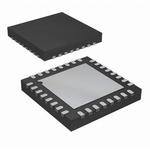
| 描述 | IC MXR 700MHZ-2.8GHZ AMP 32LFCSP |
| 产品分类 | |
| 品牌 | Analog Devices Inc |
| 数据手册 | |
| 产品图片 |
|
| 产品型号 | ADL5811ACPZ-R7 |
| PCN组件/产地 | |
| RF类型 | 通用 |
| rohs | 无铅 / 符合限制有害物质指令(RoHS)规范要求 |
| 产品系列 | - |
| 供应商器件封装 | 32-LFCSP-WQ(5x5) |
| 其它名称 | ADL5811ACPZ-R7DKR |
| 包装 | Digi-Reel® |
| 噪声系数 | 10.7dB |
| 增益 | 7.5dB |
| 封装/外壳 | 32-WFQFN 裸露焊盘,CSP |
| 标准包装 | 1 |
| 混频器数 | 1 |
| 特色产品 | http://www.digikey.com/product-highlights/cn/zh/analog-devices-adl-rf-ics/1397 |
| 电压-电源 | 3.6 V ~ 5.5 V |
| 电流-电源 | 185mA |
| 视频文件 | http://www.digikey.cn/classic/video.aspx?PlayerID=1364138032001&width=640&height=505&videoID=2245193150001 |
| 辅助属性 | 带放大器 |
| 频率 | 700MHz ~ 2.8GHz |


- 商务部:美国ITC正式对集成电路等产品启动337调查
- 曝三星4nm工艺存在良率问题 高通将骁龙8 Gen1或转产台积电
- 太阳诱电将投资9.5亿元在常州建新厂生产MLCC 预计2023年完工
- 英特尔发布欧洲新工厂建设计划 深化IDM 2.0 战略
- 台积电先进制程称霸业界 有大客户加持明年业绩稳了
- 达到5530亿美元!SIA预计今年全球半导体销售额将创下新高
- 英特尔拟将自动驾驶子公司Mobileye上市 估值或超500亿美元
- 三星加码芯片和SET,合并消费电子和移动部门,撤换高东真等 CEO
- 三星电子宣布重大人事变动 还合并消费电子和移动部门
- 海关总署:前11个月进口集成电路产品价值2.52万亿元 增长14.8%


PDF Datasheet 数据手册内容提取
High IP3, 700 MHz to 2800 MHz, Double Balanced, Passive Mixer, IF Amplifier, and Wideband LO Amplifier ADL5811 FEATURES FUNCTIONAL BLOCK DIAGRAM RF frequency: 700 MHz to 2800 MHz continuous F M P N D MM LO frequency: 250 MHz to 2800 MHz, high-side or VPI IFG NC IFO IFO NC IFG CO low-side inject 32 31 30 29 28 27 26 25 NC 1 24 NC IF range: 30 MHz to 450 MHz Power conversion gain of 7.5 dB at 1900 MHz RFCT 2 23 NC ADL5811 SSB noise figure of 10.7 dB at 1900 MHz NC 3 22 NC Input IP3 of 27.5 dBm at 1900 MHz RFIN 4 21 LOIP Input P1dB of 12.7 dBm at 1900 MHz NC 5 20 LOIN Typical LO drive of 0 dBm NC 6 19 LE Single-ended, 50 Ω RF port BIAS SERIAL Single-ended or balanced LO input port NC 7 GEN INTPEORRFATCE 18 DATA Single-supply operation: 3.6 V to 5.0 V NC 8 17 CLK 9 10 11 12 13 14 15 16 Serial port interface control on all functions E xposed paddle 5 mm × 5 mm, 32-lead LFCSP package VLO4 COMM VLO3 COMM VLO2 COMM VLO1 COMM 09912-001 Figure 1. APPLICATIONS Multiband/multistandard cellular base station receivers Wideband radio link diversity downconverters Multimode cellular extenders and broadband receivers GENERAL DESCRIPTION The ADL5811 uses revolutionary new broadband, square wideband applications where in-band blocking signals may wave limiting, local oscillator (LO) amplifiers to achieve an otherwise result in the degradation of dynamic range. Blocker unprecedented radio frequency (RF) bandwidth of 700 MHz noise figure performance is comparable to narrow-band passive to 2800 MHz. Unlike conventional narrow-band sine wave LO mixer designs. High linearity IF buffer amplifiers follow the amplifier solutions, this permits the LO to be applied either passive mixer cores, yielding typical power conversion gains of above or below the RF input over an extremely wide bandwidth. 7.5 dB, and can be used with a wide range of output Because energy storage elements are not used, the dc current impedances. For low voltage applications, the ADL5811 is consumption also decreases with decreasing LO frequency. capable of operation at voltages down to 3.6 V with substantially reduced current. Two logic bits are provided to The ADL5811 uses highly linear, doubly balanced, passive power down (<1.5 mA) the circuit when desired. mixer cores along with integrated RF and LO balancing circuits to allow single-ended operation. The ADL5811 incorporates All features of the ADL5811 are controlled via a 3-wire serial programmable RF baluns, allowing optimal performance over a port interface, resulting in optimum performance and 700 MHz to 2800 MHz RF input frequency. The balanced passive minimum external components. mixer arrangement provides outstanding LO-to-RF and LO-to- The ADL5811 is fabricated using a BiCMOS high performance IF leakages, excellent RF-to-IF isolation, and excellent IC process. The device is available in a 32-lead, 5mm × 5mm, intermodulation performance over the full RF bandwidth. LFCSP package and operates over a −40°C to +85°C The balanced mixer cores also provide extremely high input temperature range. An evaluation board is also available. linearity, allowing the device to be used in demanding Rev. 0 Information furnished by Analog Devices is believed to be accurate and reliable. However, no responsibility is assumed by Analog Devices for its use, nor for any infringements of patents or other One Technology Way, P.O. Box 9106, Norwood, MA 02062-9106, U.S.A. rights of third parties that may result from its use. Specifications subject to change without notice. No license is granted by implication or otherwise under any patent or patent rights of Analog Devices. Tel: 781.329.4700 www.analog.com Trademarks and registered trademarks are the property of their respective owners. Fax: 781.461.3113 ©2011 Analog Devices, Inc. All rights reserved.
ADL5811 TABLE OF CONTENTS Features..............................................................................................1 RF Subsystem..............................................................................20 Applications.......................................................................................1 LO Subsystem.............................................................................21 Functional Block Diagram..............................................................1 Applications Information..............................................................22 General Description.........................................................................1 Basic Connections......................................................................22 Revision History...............................................................................2 IF Port..........................................................................................22 Specifications.....................................................................................3 Bias Resistor Selection...............................................................22 Timing Characteristics................................................................4 VGS Programming....................................................................22 Absolute Maximum Ratings............................................................5 Low-Pass Filter Programming..................................................23 ESD Caution..................................................................................5 RF Balun Programming............................................................23 Pin Configuration and Function Descriptions.............................6 Register Structure...........................................................................24 Typical Performance Characteristics.............................................7 Evaluation Board............................................................................25 3.6 V Performance......................................................................16 Outline Dimensions.......................................................................28 Spurious Performance................................................................17 Ordering Guide..........................................................................28 Circuit Description.........................................................................20 REVISION HISTORY 7/11—Revision 0: Initial Version Rev. 0 | Page 2 of 28
ADL5811 SPECIFICATIONS V = 5 V, T = 25°C, f = 1900 MHz, f = 1697 MHz, RF power = −10 dBm, LO power = 0 dBm, R1 = 910 Ω, Z = 50 Ω, optimum SPI settings, S A RF LO O unless otherwise noted. Table 1. Parameter Test Conditions/Comments Min Typ Max Unit RF INPUT INTERFACE Return Loss Tunable to >20 dB broadband via serial port 15 dB Input Impedance 50 Ω RF Frequency Range 700 2800 MHz OUTPUT INTERFACE Output Impedance Differential impedance, f = 200 MHz 260||1.0 Ω||pF IF Frequency Range 30 450 MHz DC Bias Voltage1 Externally generated V V S LO INTERFACE LO Power −6 0 +10 dBm Return Loss 13 dB Input Impedance 50 Ω LO Frequency Range Low-side or high-side LO 250 2800 MHz DYNAMIC PERFORMANCE Power Conversion Gain Including 4:1 IF port transformer and PCB loss 7.5 dB Voltage Conversion Gain Z = 50 Ω, differential Z = 200 Ω differential 13.9 dB SOURCE LOAD SSB Noise Figure 10.7 dB SSB Noise Figure Under Blocking 5 dBm blocker present ±10 MHz from wanted RF input, 20.7 dB LO source filtered Input Third-Order Intercept f = 1900 MHz, f = 1901 MHz, f = 1697 MHz, 27.5 dBm RF1 RF2 LO each RF tone at −10 dBm Input Second-Order Intercept f = 1900 MHz, f = 2000 MHz, f = 1697 MHz, 62 dBm RF1 RF2 LO each RF tone at −10 dBm Input 1 dB Compression Point 12.7 dBm LO-to-IF Output Leakage Unfiltered IF output −40 dBm LO-to-RF Input Leakage −25 dBm RF-to-IF Output Isolation 26 dB IF/2 Spurious −10 dBm input power −73 dBc IF/3 Spurious −10 dBm input power −75 dBc POWER INTERFACE Supply Voltage, V 3.6 5 5.5 V S Quiescent Current Resistor programmable IF current 185 mA Power-Down Current 1.4 mA 1 Supply voltage must be applied from external circuit through choke inductors. Rev. 0 | Page 3 of 28
ADL5811 TIMING CHARACTERISTICS Low logic level ≤ 0.4 V, and high logic level ≥ 1.4 V. Table 2. Serial Interface Timing Parameter Limit Unit Test Conditions/Comments t 20 ns minimum LE setup time 1 t 10 ns minimum DATA-to-CLK setup time 2 t 10 ns minimum DATA-to-CLK hold time 3 t 25 ns minimum CLK high duration 4 t 25 ns minimum CLK low duration 5 t 10 ns minimum CLK-to-LE setup time 6 t 20 ns minimum LE pulse width 7 Timing Diagram t t 4 5 CLK t t 2 3 DB2 DB1 DB0(LSB) DATA DB23(MSB) DB22 (CONTROLBITC3) (CONTROLBITC2) (CONTROLBITC1) t6 t7 t1 LE 09912-002 Figure 2. Timing Diagram Rev. 0 | Page 4 of 28
ADL5811 ABSOLUTE MAXIMUM RATINGS Stresses above those listed under Absolute Maximum Ratings may cause permanent damage to the device. This is a stress Table 3. rating only; functional operation of the device at these or any Parameter Rating other conditions above those indicated in the operational Supply Voltage, VPOS 5.5 V section of this specification is not implied. Exposure to absolute CLK, DATA, LE 5.5 V maximum rating conditions for extended periods may affect IF Output Bias 6.0 V device reliability. RF Input Power 20 dBm LO Input Power 13 dBm Internal Power Dissipation 1.1 W ESD CAUTION θ (Exposed Paddle Soldered Down) 25°C/W JA Maximum Junction Temperature 150°C Operating Temperature Range −40°C to +85°C Storage Temperature Range −65°C to +150°C Rev. 0 | Page 5 of 28
ADL5811 PIN CONFIGURATION AND FUNCTION DESCRIPTIONS M FM PN DM VPIIFGNCIFOIFONCIFGCO 21098765 33322222 NC 1 24 NC RFCT 2 23 NC NC 3 ADL5811 22 NC RFIN 4 21 LOIP TOP VIEW NC 5 20 LOIN (Not to Scale) NC 6 19 LE NC 7 18 DATA NC 8 17 CLK 910111213141516 4M3M2M1M OMOMOMOM VLOVLOVLOVLO C C C C NOTES 1. NC = NO CONNECT. CAN BE GROUNDED. 2 . ETOXP GORSOEUDN PDA.D MUST BE CONNECTED 09912-003 Figure 3. Pin Configuration Table 4. Pin Function Descriptions Pin No. Mnemonic Description 1, 3, 5 to 8, 22 to 24, 27, 30 NC No Connect. Can be grounded. 2 RFCT RF Balun Center Tap (AC Ground). 4 RFIN RF Input. Should be ac-coupled. 9, 11, 13, 15 VLO4, VLO3, VLO2, VLO1 Positive Supply Voltages for LO Amplifier. 10, 12, 14, 16, 25 COMM Ground. 17, 18, 19 CLK, DATA, LE Serial Port Interface Control. 20 LOIN Ground Return for LO Input. 21 LOIP LO Input. Should be ac-coupled. 26 IFGD Supply Return for IF Amplifier. Must be grounded. 28, 29 IFOP, IFON IF Differential Open-Collector Outputs. Should be pulled up to V using CC external inductors. 31 IFGM IF Amplifier Bias Control. 32 VPIF Supply Voltage for IF Amplifier. EPAD Exposed pad must be connected to ground. Rev. 0 | Page 6 of 28
ADL5811 TYPICAL PERFORMANCE CHARACTERISTICS V = 5 V, T = 25°C, f = 1900 MHz, f = 1697 MHz, RF power = −10 dBm, LO power = 0 dBm, R1 = 910 Ω, Z = 50 Ω, optimum SPI settings, S A RF LO O unless otherwise noted. 220 90 TA = –40°C TA = –40°C 210 TTAA == ++2855°°CC 80 TTAA == ++2855°°CC 200 70 mA) 190 NT ( 180 Bm) 60 CURRE 170 T IP2 (d 50 PLY 160 NPU 40 P I U 150 S 30 140 20 130 120 10 700 900 1100 1300RF15 F0R0E1Q7U0E0N1C9Y0 0(M2H1z0)0 2300 2500 2700 09912-004 700 900 1100 1300RF1 5F0R0EQ17U0E0NC19Y0 0(MH21z0)0 2300 2500 2700 09912-007 Figure 4. Supply Current vs. RF Frequency Figure 7. Input IP2 vs. RF Frequency 10 20 TA = –40°C TA = –40°C TA = +25°C 18 TA = +25°C 9 TA = +85°C TA = +85°C 16 8 AIN (dB) 7 dBm) 1124 ON G 6 1dB ( 10 ONVERSI 5 INPUT P 68 C 4 4 3 2 2700 900 1100 1300RF1 5F0R0EQ17U0E0NC19Y0 0(MH21z0)0 2300 2500 2700 09912-005 0700 900 1100 1300RF1 5F0R0EQ17U0E0NC19Y0 0(MH21z0)0 2300 2500 2700 09912-008 Figure 5. Power Conversion Gain vs. RF Frequency Figure 8. Input P1dB vs. RF Frequency 45 16 40 TTTAAA === ++–428055°°°CCC 15 TTTAAA === ++–428055°°°CCC 14 35 B) 13 Bm) E (d 12 d 30 R NPUT IP3 ( 25 OISE FIGU 1101 I N 9 20 8 15 7 10700 900 1100 1300RF1 5F0R0EQ17U0E0NC19Y0 0(MH21z0)0 2300 2500 2700 09912-006 6700 900 1100 1300RF15 F0R0E1Q7U0E0N1C9Y0 0(M2H1z0)0 2300 2500 2700 09912-009 Figure 6. Input IP3 vs. RF Frequency Figure 9. SSB Noise Figure vs. RF Frequency Rev. 0 | Page 7 of 28
ADL5811 235 80 RF = 1900MHz VPOS= 4.75V RF = 1900MHz VPOS= 4.75V 225 VPOS= 5.00V 75 VPOS= 5.00V VPOS= 5.25V VPOS= 5.25V 215 70 A) 205 65 m NT ( 195 Bm) 60 RRE 185 P2 (d 55 CU T I PLY 175 NPU 50 P I U 165 45 S 155 40 145 35 135–40 –30 –20 –10 0TEM10PER2A0TU3R0E (°4C0) 50 60 70 80 09912-010 30–40 –30 –20 –10 0TE1M0PER2A0TU3R0E (°4C0) 50 60 70 80 09912-013 Figure 10. Supply Current vs. Temperature Figure 13. Input IP2 vs. Temperature 10.0 20 RF = 1900MHz VPOS= 4.75V RF = 1900MHz VPOS= 4.75V 9.5 VPOS= 5.00V VPOS= 5.00V VPOS= 5.25V 18 VPOS= 5.25V 9.0 16 AIN (dB) 88..05 dBm) 14 ON G 7.5 1dB ( 12 NVERSI 7.0 NPUT P 10 O 6.5 I C 8 6.0 6 5.5 5.0–40 –30 –20 –10 0TE1M0PER2A0TU3R0E (°4C0) 50 60 70 80 09912-011 4–40 –30 –20 –10 0TE1M0PER2A0TU3R0E (°4C0) 50 60 70 80 09912-014 Figure 11. Power Conversion Gain vs. Temperature Figure 14. Input P1dB vs. Temperature 35 15 RF = 1900MHz VPOS= 4.75V RF = 1900MHz VPOS= 4.75V 33 VPOS= 5.00V VPOS= 5.00V VPOS= 5.25V 14 VPOS= 5.25V 31 29 dB) 13 m) E ( B 27 R d U 12 PUT IP3 ( 2235 OISE FIG 11 N N I B 21 S 10 S 19 9 17 15 8 –40 –30 –20 –10 0TE1M0PER2A0TU3R0E (°4C0) 50 60 70 80 09912-012 –40 –30 –20 –10 0TE1M0PER2A0TU3R0E (°4C0) 50 60 70 80 09912-015 Figure 12. Input IP3 vs. Temperature Figure 15. SSB Noise Figure vs. Temperature Rev. 0 | Page 8 of 28
ADL5811 200 80 TA = 25°C RF = 900MHz TA = 25°C RF = 1900MHz 195 RF = 2500MHz 70 190 60 A) m NT ( 185 Bm) 50 CURRE 180 T IP2 (d 40 PLY 175 NPU 30 P I U S 170 20 165 10 RF = 900MHz RF = 1900MHz RF = 2500MHz 160 0 30 80 130 I1F8 0FREQ2U3E0NCY2 (8M0Hz)330 380 430 09912-016 30 80 130 I1F8 0FREQ2U3E0NCY2 (8M0Hz)330 380 430 09912-019 Figure 16. Supply Current vs. IF Frequency Figure 19. Input IP2 vs. IF Frequency 11 18 TA = 25°C RF = 900MHz TA = 25°C RF = 900MHz RF = 1900MHz RF = 1900MHz 10 RF = 2500MHz 16 RF = 2500MHz B) 9 14 ON GAIN (d 8 1dB (dBm) 1102 NVERSI 7 NPUT P 8 O 6 I C 6 5 4 4 2 30 80 130 I1F8 0FREQ2U3E0NCY2 (8M0Hz)330 380 430 09912-017 30 80 130 I1F8 0FREQ2U3E0NCY2 (8M0Hz)330 380 430 09912-020 Figure 17. Power Conversion Gain vs. IF Frequency Figure 20. Input P1dB vs. IF Frequency 30 20 TA = 25°C RF = 900MHz TA = 25°C RF = 900MHz RF = 1900MHz RF = 1900MHz 39 RF = 2500MHz 18 RF = 2500MHz 28 B) 16 d Bm) 27 RE ( 14 d U P3 ( 26 FIG 12 NPUT I 25 NOISE 10 I B S 24 S 8 23 6 2230 80 130 I1F8 0FREQ2U3E0NCY2 (8M0Hz)330 380 430 09912-018 430 80 130 I1F8 0FREQ2U3E0NCY2 (8M0Hz)330 380 430 09912-021 Figure 18. Input IP3 vs. IF Frequency Figure 21. SSB Noise Figure vs. IF Frequency Rev. 0 | Page 9 of 28
ADL5811 11 20 TA = 25°C RF = 900MHz TA = 25°C RF = 900MHz RF = 1900MHz RF = 1900MHz 10 RF = 2500MHz 18 RF = 2500MHz B) 9 16 AIN (d 8 dBm) 14 ON G 7 1dB ( 12 RSI T P VE 6 PU 10 N N O I C 5 8 4 6 3 4 –6 –4 –2 L0O POW2ER (dBm4) 6 8 10 09912-022 –6 –4 –2 L0O POW2ER (dBm4) 6 8 10 09912-025 Figure 22. Power Conversion Gain vs. LO Power Figure 25. Input P1dB vs. LO Power 35 –40 33 TA = 25°C RRRFFF === 12995000000MMMHHHzzz –45 TTTAAA === ++–428055°°°CCC 31 –50 29 c) –55 m) dB dB 27 S ( –60 T IP3 ( 25 URIOU –65 PU 23 SP –70 IN 21 IF/2 –75 19 –80 17 –85 15–6 –4 –2 L0O POW2ER (dBm4) 6 8 10 09912-023 –90700 900 1100 1300RF15 F0R0EQ17U0E0N1C9Y0 0(MH21z0)0 2300 2500 2700 09912-026 Figure 23. Input IP3 vs. LO Power Figure 26. IF/2 Spurious vs. RF Frequency, RF Power = −10 dBm 80 –55 TA = 25°C TA = –40°C TA = +25°C 70 –60 TA = +85°C 60 c) –65 m) dB 2 (dB 50 OUS ( –70 UT IP 40 PURI –75 P S IN F/3 30 I –80 20 RF = 900MHz –85 RF = 1900MHz RF = 2500MHz 10 –90 –6 –4 –2 L0O POW2ER (dBm4) 6 8 10 09912-024 700 900 1100 1300RF1 5F0R0EQ17U0E0NC19Y0 0(MH21z0)0 2300 2500 2700 09912-027 Figure 24. Input IP2 vs. LO Power Figure 27. IF/3 Spurious vs. RF Frequency, RF Power = −10 dBm Rev. 0 | Page 10 of 28
ADL5811 100 500 10 MEAN: 7.5 TA = 25°C RF = 900MHz SD: 0.12% RF = 1900MHz RF = 2500MHz 80 400 8 %) Ω) pF) GE ( 60 CE ( 300 6 CE ( A N N PERCENT 40 RESISTA 200 4 CAPACITA 20 100 2 07.1 7.3 CONVERSIO7.N5 GAIN (dB) 7.7 7.9 09912-028 030 80 130 1IF8 0FREQ23U0ENCY2 8(0MHz)330 380 430 0 09912-031 Figure 28. Conversion Gain Distribution Figure 31. IF Output Impedance (R Parallel C Equivalent) 100 0 MEAN: 27.5 TA = +25°C SD: 0.36% –5 80 dB) –10 %) SS ( GE ( 60 N LO –15 A R T U –20 N T E E PERC 40 ORT R –25 P F –30 20 R –35 0 –40 23.5 25.5 INPUT2 I7P.35 (dBm) 29.5 31.5 09912-029 700 900 1100 1300RF15 F0R0E1Q7U0E0N1C9Y0 0(M2H1z0)0 2300 2500 2700 09912-032 Figure 29. Input IP3 Distribution Figure 32. RF Port Return Loss, Fixed IF vs. RF Frequency 100 0 MEAN: 11.68 TA = 25°C SD: 0.36% –3 80 –6 B) E (%) 60 SS (d –9 G O A L NT RN –12 ERCE 40 RETU –15 P O L –18 20 –21 0 –24 10.5 11.0 INPUT P111.d5B (dBm) 12.0 12.5 09912-030 500 700 900 1100LO13 F0R0EQ15U0E0N1C7Y0 0(MH19z0)0 2100 2300 2500 09912-033 Figure 30. Input P1dB Distribution Figure 33. LO Return Loss Rev. 0 | Page 11 of 28
ADL5811 0 0 TTAA == +–4205°°CC 22LLOO--TTOO--IRFF TA = 25°C –10 TA = +85°C –10 dB) –20 m) –20 ATION ( –30 GE (dB –30 OL –40 KA S A O-IF I –50 O LE –40 T L RF- –60 2X –50 –70 –60 –80700 900 1100 1300RF15 F0R0E1Q7U0E0N1C9Y0 0(M2H1z0)0 2300 2500 2700 09912-034 –70500 700 900 1100LO13 F0R0E1Q5U0E0N1C7Y0 0(M1H9z0)0 2100 2300 2500 09912-037 Figure 34. RF-to-IF Isolation vs. RF Frequency Figure 37. 2XLO Leakage vs. LO Frequency 0 –10 TA = –40°C 3LO-TO-IF TA = 25°C TA = +25°C 3LO-TO-RF –10 TA = +85°C –20 Bm) –20 m) –30 AGE (d –30 GE (dB –40 AK –40 KA E A F L LE –50 O-TO-I –50 3XLO –60 L –60 –70 –70 –80 –80 500 700 900 1100LO13 F0R0E1Q5U0E0N1C7Y0 0(MH19z0)0 2100 2300 2500 09912-035 500 700 900 1100LO13 F0R0E1Q5U0E0N1C7Y0 0(M1H9z0)0 2100 2300 2500 09912-038 Figure 35. LO-to-IF Leakage vs. LO Frequency Figure 38. 3XLO Leakage vs. LO Frequency 0 14 16 TA = –40°C TA = +25°C TA = +25°C 13 15 –10 TA = +85°C 12 14 LO-TO-RF LEAKAGE (dBm) –––––6543200000 CONVERSION GAIN (dB) 1107891 NOISE FIGUGRAEIN 911111023 SSB NOISE FIGURE (dB) 6 8 –70 5 7 VGS = 0 VGS = 2 VGS = 4 VGS = 6 VGS = 1 VGS = 3 VGS = 5 VGS = 7 –80500 700 900 1100LO13 F0R0E1Q5U0E0N1C7Y0 0(MH19z0)0 2100 2300 2500 09912-036 4700 900 1100 1300RF1 5F0R0EQ17U0E0NC19Y0 0(MH21z0)0 2300 2500 2700 09912-0139 Figure 36. LO-to-RF Leakage vs. LO Frequency Figure 39. Power Conversion Gain and SSB Noise Figure vs. RF Frequency for All VGS Settings Rev. 0 | Page 12 of 28
ADL5811 35 27 240 VGS = 0 VGS = 2 VGS = 4 VGS = 6 TA = +25°C TA = 25°C RF = 900MHz VGS = 1 VGS = 3 VGS = 5 VGS = 7 RF = 1900MHz RF = 2500MHz 30 24 220 INPUT IP3 25 21 A) 200 INPUT IP3 (dBm) 112050 111258 INPUT P1dB (dBm) SUPPLY CURRENT (m 111468000 5 9 120 INPUT P1dB 0700 900 1100 1300RF1 5F0R0EQ17U0E0NC19Y0 (0MH21z0)0 2300 2500 2700 6 09912-140 100600 700 800 900IF 1B0I0A0S1 R10E0SI1S2T0O0R13V0A0L1U4E0 0(Ω1)500160017001800 09912-042 Figure 40. Input IP3 and Input P1dB vs. RF Frequency for All VGS Settings Figure 42. Supply Current vs. IF Bias Resistor Value 3305 RRRFFF === 12995000000MMMHHHzzz RE (dB) 1280 TA = 25°C INPUT IP3 RRRFFF === 12995000000MMMHHHzzz 2382 U G B) 25 E FI 16 24 d S SSB NOISE FIGURE ( 112050 N GAIN AND SSB NOI 1110248 NOISE FGIAGIUNRE 8112260 INPUT IP3 (dBm) O SI 5 ER 6 4 V TA = +25°C ON 0 C 4 0 –30 –25 –20 BLO–1C5KER P–1O0WER (–d5Bm) 0 5 10 09912-141 600 700 800 90I0F 1B0IA00S 1R1E00SI1S2T0O0R1 3V0A0L1U4E00 (Ω1)500160017001800 09912-043 Figure 41. SSB Noise Figure vs. 10 MHz Offset Blocker Level Figure 43. Power Conversion Gain, SSB Noise Figure, and Input IP3 vs. IF Bias Resistor Value Rev. 0 | Page 13 of 28
ADL5811 11 18 RRFFBB == 01 TA = +25°C RRFFBB == 01 TA = +25°C 10 RFB = 2 17 RFB = 2 RFB = 3 RFB = 3 RFB = 4 RFB = 4 9 RFB = 5 16 RFB = 5 RFB = 6 RFB = 6 AIN (dB) 78 RFB = 7 dBm) 1145 RFB = 7 ON G 6 1dB ( 13 ONVERSI 45 INPUT P 1121 C 3 10 2 9 1700 900 1100 1300RF15 F0R0E1Q7U0E0N1C9Y0 0(M2H1z0)0 2300 2500 2700 09912-044 8700 900 1100 1300RF1 5F0R0EQ17U0E0NC19Y0 0(MH21z0)0 2300 2500 2700 09912-046 Figure 44. Conversion Gain vs. RF Frequency for All RFB Settings Figure 46. Input P1dB vs. RF Frequency for All RFB Settings 23339012 RRRRRRRRFFFFFFFFBBBBBBBB ======== 01234567 TA = +25°C dB) 11113456 RRRRRRRRFFFFFFFFBBBBBBBB ======== 01234567 TA = +25°C Bm) 28 URE ( 12 INPUT IP3 (d 222567 SSB NOISE FIG 11091 24 8 23 7 22700 900 1100 1300RF1 5F0R0EQ17U0E0NC19Y0 0(MH21z0)0 2300 2500 2700 09912-045 6700 900 1100 1300RF15 F0R0E1Q7U0E0N1C9Y0 0(MH21z0)0 2300 2500 2700 09912-047 Figure 45. Input IP3 vs. RF Frequency for All RFB Settings Figure 47. SSB Noise Figure vs. RF Frequency for All RFB Settings Rev. 0 | Page 14 of 28
ADL5811 12 21 LLPPFF == 01 TA = +25°C LLPPFF == 01 TA = +25°C 10 LLPPFF == 23 RFB0 19 LLPPFF == 23 17 RFB0 B) 8 ON GAIN (d 6 1dB (dBm) 1135 NVERSI 4 RFB7 NPUT P 11 CO 2 I 9 RFB7 0 7 –2 5 700 900 1100 1300RF1 5F0R0EQ17U0E0NC19Y0 0(MH21z0)0 2300 2500 2700 09912-048 700 900 1100 1300RF15 F0R0E1Q7U0E0N1C9Y0 0(M2H1z0)0 2300 2500 2700 09912-050 Figure 48. Conversion Gain vs. RF Frequency for All LPF Settings at Figure 50. Input P1dB vs. RF Frequency for All LPF Settings at RFB7 and RFB0 RFB7 and RFB0 35 20 TA = +25°C LLPPFF == 01 TA = +25°C 33 18 LPF = 2 RFB0 LPF = 3 31 16 RFB0 B) m) 29 E (d 14 T IP3 (dB 2257 SE FIGUR 1102 INPU 23 RFB7 B NOI 8 RFB7 21 S S 6 19 LPF = 0 17 LPF = 1 4 LPF = 2 LPF = 3 15700 900 1100 1300RF15 F0R0EQ17U0E0N1C9Y0 0(MH21z0)0 2300 2500 2700 09912-049 2700 900 1100 1300RF15 F0R0E1Q7U0E0N1C9Y0 0(M2H1z0)0 2300 2500 2700 09912-051 Figure 49. Input IP3 vs. RF Frequency for All LPF Settings at RFB7 and RFB0 Figure 51. SSB Noise Figure vs. RF Frequency for All LPF Settings at RFB7 and RFB0 Rev. 0 | Page 15 of 28
ADL5811 3.6 V PERFORMANCE V = 3.6 V, T = 25°C, f = 1900 MHz, f = 1697 MHz, RF power = −10 dBm, LO power = 0 dBm, R1 = 800 Ω, Z = 50 Ω, optimum SPI settings, S A RF LO O unless otherwise noted. 150 80 TA = –40°C TA = –40°C TA = +25°C TA = +25°C 140 TA = +85°C 70 TA = +85°C 130 60 A) m NT ( 120 Bm) 50 CURRE 110 T IP2 (d 40 PLY 100 NPU 30 P I U S 90 20 80 10 70 0 700 900 1100 1300RF15 F0R0E1Q7U0E0N1C9Y0 0(M2H1z0)0 2300 2500 2700 09912-052 700 900 1100 1300RF15 F0R0EQ17U0E0NC19Y0 0(MH21z0)0 2300 2500 2700 09912-055 Figure 52. Supply Current vs. RF Frequency at 3.6 V Figure 55. Input IP2 vs. RF Frequency at 3.6 V 14 24 TA = –40°C TA = –40°C TA = +25°C TA = +25°C 12 TA = +85°C 21 TA = +85°C 18 B) 10 ON GAIN (d 8 1dB (dBm) 1125 RSI 6 T P VE PU 9 N N CO 4 I 6 2 3 0 0 700 900 1100 1300RF15 F0R0EQ17U0E0N1C9Y0 0(MH21z0)0 2300 2500 2700 09912-053 700 900 1100 1300RF1 5F0R0EQ17U0E0NC19Y0 0(MH21z0)0 2300 2500 2700 09912-056 Figure 53. Power Conversion Gain vs. RF Frequency at 3.6 V Figure 56. Input P1dB vs. RF Frequency at 3.6 V 35 24 TA = –40°C TA = –40°C TA = +25°C TA = +25°C 30 TA = +85°C 21 TA = +85°C 25 B) 18 d INPUT IP3 (dBm) 1250 B NOISE FIGURE ( 11259 10 SS 6 5 3 0700 900 1100 1300RF15 F0R0EQ17U0E0N1C9Y0 0(MH21z0)0 2300 2500 2700 09912-054 0700 900 1100 1300RF15 F0R0E1Q7U0E0N1C9Y0 0(M2H1z0)0 2300 2500 2700 09912-057 Figure 54. Input IP3 vs. RF Frequency at 3.6 V Figure 57. SSB Noise Figure vs. RF Frequency at 3.6 V Rev. 0 | Page 16 of 28
ADL5811 SPURIOUS PERFORMANCE (N × f ) − (M × f ) spur measurements were made using the standard evaluation board. Mixer spurious products are measured in RF LO dBc from the IF output power level. Data was measured only for frequencies less than 6 GHz. Typical noise floor of the measurement system = −100 dBm. 5 V Performance V = 5 V, T = 25°C, RF power = −10 dBm, LO power = 0 dBm, R1 = 910 Ω, Z = 50 Ω, optimum SPI settings, unless otherwise noted. S A O Table 5. RF = 900 MHz, LO = 697 MHz M 0 1 2 3 4 5 6 7 8 9 10 11 12 13 14 15 0 −54.2 −31.4 −41.5 −29.4 −58.5 −49.3 −70.5 −52.9 1 −37.8 0.0 −38.7 −19.6 −51.6 −38.0 −62.9 −52.4 −70.2 −57.9 2 −65.0 −54.4 −69.6 −53.4 −72.5 −82.3 −93.5 −97.4 −93.0 −98.8 <−100 <−100 3 −94.0 −86.7 <−100 −91.0 <−100 −95.3 <−100 <−100 <−100 <−100 <−100 <−100 <−100 4 <−100 <−100 <−100 <−100 <−100 <−100 <−100 <−100 <−100 <−100 <−100 <−100 <−100 <−100 5 <−100 <−100 <−100 <−100 <−100 <−100 <−100 <−100 <−100 <−100 <−100 <−100 <−100 <−100 <−100 <−100 6 <−100 <−100 <−100 <−100 <−100 <−100 <−100 <−100 <−100 <−100 <−100 <−100 <−100 <−100 <−100 <−100 7 <−100 <−100 <−100 <−100 <−100 <−100 <−100 <−100 <−100 <−100 <−100 <−100 <−100 <−100 <−100 N 8 <−100 <−100 <−100 <−100 <−100 <−100 <−100 <−100 <−100 <−100 <−100 <−100 <−100 <−100 9 <−100 <−100 <−100 <−100 <−100 <−100 <−100 <−100 <−100 <−100 <−100 <−100 10 <−100 <−100 <−100 <−100 <−100 <−100 <−100 <−100 <−100 <−100 <−100 11 <−100 <−100 <−100 <−100 <−100 <−100 <−100 <−100 <−100 <−100 12 <−100 <−100 <−100 <−100 <−100 <−100 <−100 <−100 <−100 13 <−100 <−100 <−100 <−100 <−100 <−100 <−100 14 <−100 <−100 <−100 <−100 <−100 <−100 15 <−100 <−100 <−100 <−100 <−100 Table 6. RF = 1900 MHz, LO = 1697 MHz M 0 1 2 3 4 5 6 7 8 9 10 11 12 13 14 15 0 −34.9 −30.7 −66.0 1 −33.2 0.0 −56.6 −51.3 −77.8 2 −75.0 −78.5 −71.5 −85.2 −80.3 <−100 3 <−100 <−100 <−100 −89.5 −94.8 <−100 <−100 4 <−100 <−100 <−100 <−100 <−100 <−100 <−100 <−100 5 <−100 <−100 <−100 <−100 <−100 <−100 <−100 6 <−100 <−100 <−100 <−100 <−100 <−100 <−100 7 <−100 <−100 <−100 <−100 <−100 <−100 <−100 N 8 <−100 <−100 <−100 <−100 <−100 <−100 <−100 9 <−100 <−100 <−100 <−100 <−100 <−100 <−100 10 <−100 <−100 <−100 <−100 <−100 <−100 <−100 11 <−100 <−100 <−100 <−100 <−100 <−100 <−100 12 <−100 <−100 <−100 <−100 <−100 <−100 13 <−100 <−100 <−100 <−100 14 <−100 <−100 <−100 15 <−100 <−100 Rev. 0 | Page 17 of 28
ADL5811 Table 7. RF = 2500 MHz, LO = 2297 MHz M 0 1 2 3 4 5 6 7 8 9 10 11 12 13 14 15 0 −28.6 −45.7 1 −32.5 0.0 −53.0 −52.4 2 −91.2 −82.8 −60.5 −80.8 −97.3 3 <−100 <−100 −87.7 <−100 <−100 4 <−100 <−100 <−100 <−100 <−100 5 <−100 <−100 <−100 <−100 <−100 <−100 6 <−100 <−100 <−100 <−100 <−100 <−100 7 <−100 <−100 <−100 <−100 <−100 N 8 <−100 <−100 <−100 <−100 <−100 9 <−100 <−100 <−100 <−100 <−100 10 <−100 <−100 <−100 <−100 <−100 11 <−100 <−100 <−100 <−100 <−100 12 <−100 <−100 <−100 <−100 <−100 13 <−100 <−100 <−100 <−100 14 <−100 <−100 <−100 15 <−100 <−100 3.6 V Performance V = 3.6 V, T = 25°C, RF power = −10 dBm, LO power = 0 dBm, R1 = 800 Ω, Z = 50 Ω, optimum SPI settings, unless otherwise noted. S A O Table 8. RF = 900 MHz, LO = 697 MHz M 0 1 2 3 4 5 6 7 8 9 10 11 12 13 14 15 0 −45.5 −35.1 −44.1 −30.2 −49.9 −48.7 −66.6 −66.5 1 −41.0 0.0 −37.3 −18.9 −54.8 −40.4 −62.4 −53.2 −73.0 −66.8 2 −59.2 −54.7 −78.2 −54.8 −62.8 −83.1 −78.3 −96.1 −79.5 −96.2 −96.2 <−100 3 −90.0 −81.9 <−100 −73.9 −89.6 −79.4 <−100 −95.3 <−100 <−100 <−100 <−100 <−100 4 <−100 <−100 <−100 <−100 <−100 <−100 <−100 <−100 <−100 <−100 <−100 <−100 <−100 <−100 5 <−100 <−100 <−100 <−100 <−100 <−100 <−100 <−100 <−100 <−100 <−100 <−100 <−100 <−100 <−100 <−100 6 <−100 <−100 <−100 <−100 <−100 <−100 <−100 <−100 <−100 <−100 <−100 <−100 <−100 <−100 <−100 <−100 7 <−100 <−100 <−100 <−100 <−100 <−100 <−100 <−100 <−100 <−100 <−100 <−100 <−100 <−100 <−100 N 8 <−100 <−100 <−100 <−100 <−100 <−100 <−100 <−100 <−100 <−100 <−100 <−100 <−100 <−100 9 <−100 <−100 <−100 <−100 <−100 <−100 <−100 <−100 <−100 <−100 <−100 <−100 10 <−100 <−100 <−100 <−100 <−100 <−100 <−100 <−100 <−100 <−100 <−100 11 <−100 <−100 <−100 <−100 <−100 <−100 <−100 <−100 <−100 <−100 12 <−100 <−100 <−100 <−100 <−100 <−100 <−100 <−100 <−100 13 <−100 <−100 <−100 <−100 <−100 <−100 <−100 14 <−100 <−100 <−100 <−100 <−100 <−100 15 <−100 <−100 <−100 <−100 <−100 Rev. 0 | Page 18 of 28
ADL5811 Table 9. RF = 1900 MHz, LO = 1697 MHz M 0 1 2 3 4 5 6 7 8 9 10 11 12 13 14 15 0 −46.6 −30.5 −78.5 1 −33.4 0.0 −57.0 −53.8 −79.5 2 −68.9 −77.2 −69.2 −72.8 −75.2 <−100 3 <−100 <−100 <−100 −74.4 −94.0 <−100 <−100 4 <−100 <−100 <−100 <−100 <−100 <−100 <−100 <−100 5 <−100 <−100 <−100 <−100 <−100 <−100 <−100 6 <−100 <−100 <−100 <−100 <−100 <−100 <−100 7 <−100 <−100 <−100 <−100 <−100 <−100 <−100 N 8 <−100 <−100 <−100 <−100 <−100 <−100 <−100 9 <−100 <−100 <−100 <−100 <−100 <−100 <−100 10 <−100 <−100 <−100 <−100 <−100 <−100 <−100 11 <−100 <−100 <−100 <−100 <−100 <−100 <−100 12 <−100 <−100 <−100 <−100 <−100 <−100 13 <−100 <−100 <−100 <−100 14 <−100 <−100 <−100 15 <−100 <−100 Table 10. RF = 2500 MHz, LO = 2297 MHz M 0 1 2 3 4 5 6 7 8 9 10 11 12 13 14 15 0 −30.0 −51.1 1 −32.1 0.0 −53.6 −51.7 2 −89.0 −78.0 −65.5 −72.9 −88.2 3 <−100 <−100 −73.5 <−100 <−100 4 <−100 <−100 <−100 <−100 <−100 5 <−100 <−100 <−100 <−100 <−100 <−100 6 <−100 <−100 <−100 <−100 <−100 <−100 7 <−100 <−100 <−100 <−100 <−100 N 8 <−100 <−100 <−100 <−100 <−100 9 <−100 <−100 <−100 <−100 <−100 10 <−100 <−100 <−100 <−100 <−100 11 <−100 <−100 <−100 <−100 <−100 12 <−100 <−100 <−100 <−100 <−100 13 <−100 <−100 <−100 <−100 14 <−100 <−100 <−100 15 <−100 <−100 Rev. 0 | Page 19 of 28
ADL5811 CIRCUIT DESCRIPTION The ADL5811 consists of two primary components: the RF The resulting balanced RF signal is applied to a passive mixer subsystem and the LO subsystem. The combination of design, that commutates the RF input in accordance with the output of the process, and packaging technology allows the functions of these LO subsystem. The passive mixer is essentially a balanced, low subsystems to be integrated into a single die, using mature loss switch that adds minimum noise to the frequency translation. packaging and interconnection technologies to provide a high The only noise contribution from the mixer is due to the resistive performance device with excellent electrical, mechanical, and loss of the switches, which is in the order of a few ohms. thermal properties. The wideband frequency response and Because the mixer is inherently broadband and bidirectional, it flexible frequency programming simplifies the receiver design, is necessary to properly terminate all idler (M × N product) saves on-board space, and minimizes the need for external frequencies generated by the mixing process. Terminating the components. mixer avoids the generation of unwanted intermodulation The RF subsystem consists of an integrated, tunable, low loss RF products and reduces the level of unwanted signals at the input balun; a double balanced, passive MOSFET mixer; a tunable sum of the IF amplifier, where high peak signal levels can compromise termination network; and an IF amplifier. the compression and intermodulation performance of the system. This termination is accomplished by the addition of a The LO subsystem consists of a multistage limiting LO amplifier. programmable low-pass filter network between the IF amplifier The purpose of the LO subsystem is to provide a large, fixed and the mixer and in the feedback elements in the IF amplifier. amplitude, balanced signal to drive the mixer independent of the level of the LO input. A block diagram of the device is The IF amplifier is a balanced feedback design that simultaneously shown in Figure 58. provides the desired gain, noise figure, and input impedance M that is required to achieve the overall performance. The balanced F M P N D M VPI IFG NC IFO IFO NC IFG CO open-collector output of the IF amplifier, with an impedance 32 31 30 29 28 27 26 25 modified by the feedback within the amplifier, permits the NC 1 24 NC output to be connected directly to a high impedance filter, a RFCT 2 23 NC differential amplifier, or an analog-to-digital converter (ADC) ADL5811 input while providing optimum second-order intermodulation NC 3 22 NC suppression. The differential output impedance of the IF amplifier RFIN 4 21 LOIP is approximately 200 Ω. If operation in a 50 Ω system is desired, NC 5 20 LOIN the output can be transformed to 50 Ω by using a 4:1 transformer NC 6 19 LE or an LC impedance matching network. BIAS SERIAL NC 7 GEN PORT 18 DATA INTERFACE The intermodulation performance of the design is generally NC 8 17 CLK limited by the IF amplifier. The IP3 performance can be optimized 9 10 11 12 13 14 15 16 by adjusting the low-pass filter between the mixer and the IF VLO4 COMM VLO3 COMM VLO2 COMM VLO1 COMM 09912-162 amplifier. Further optimization can be made by adjusting the IF Figure 58. Block Diagram current with an external resistor. Figure 42 and Figure 43 illustrate how various IF resistors affect the performance with a 5 V RF SUBSYSTEM supply. Additionally, dc current can be saved by increasing the The single-ended, 50 Ω RF input is internally transformed to a IF resistor. It is permissible to reduce the IF amplifier’s dc balanced signal using a tunable, low loss, unbalanced-to-balanced supply voltage to as low as 3.3 V, further reducing the dissipated (balun) transformer. This transformer is made possible by an power of the part. (Note that no performance enhancement is extremely low loss metal stack, which provides both excellent obtained by reducing the value of these resistors, and excessive balance and dc isolation for the RF port. Although the port can dc power dissipation may result.) be dc connected, it is recommended that a blocking capacitor be Because the mixer is bidirectional, the tuning of the RF and IF used to avoid running excessive dc current through the part. ports is linked and it is possible for the user to optimize gain, The RF balun can easily support an RF input frequency range of noise figure, IP3, and impedance match via the SPI. This feature 700 MHz to 2800 MHz. This balun is tuned over the frequency permits high performance operation and is achieved entirely range by SPI controlled switched capacitor networks at the using SPI control. Additionally, the performance of the mixer can input and output of the RF balun. be improved by setting the optimum gate voltage on the passive mixer, which is also controlled by the SPI to enable optimum performance of the part. See the Applications Information section for examples of this tuning. Rev. 0 | Page 20 of 28
ADL5811 LO SUBSYSTEM obtained with a 0 dBm input level; however, the circuit continues to function at considerably lower levels of LO input power. The LO amplifier is designed to provide a large signal level to the mixer to obtain optimum intermodulation and compression The performance of this amplifier is critical in achieving a high performance. The resulting LO amplifier provides very high intercept passive mixer without degrading the noise floor of the performance over a wide range of LO input frequencies. system. This is a critical requirement in an interferer rich environment, such as cellular infrastructure, where blocking The ideal waveshape for switching the passive mixer is a square interferers can limit mixer performance. Blocking dynamic wave at the LO frequency to cause the mixer to switch through range can benefit from a higher level of LO drive, which pushes its resistive region (from on to off and off to on) as rapidly as the LO amplifier stages harder into compression and causes them possible. While it has always been possible to generate such a to switch harder and to limit the small signal gain of the chain. square wave, the amount of dc current required to generate a Both of these conditions are beneficial to low noise figure under large amplitude square wave at high frequencies has made it blocking. NF under blocking can be improved several decibels impractical to create such a mixer. Novel circuitry within the for LO input power levels above 0 dBm. ADL5811 permits the generation of a near-square wave output at frequencies of up to 2800 MHz with dc current that compares The LO amplifier topology inherently minimizes the dc current favorably with that employed by narrow-band passive mixers. based on the LO operating voltage and the LO operating frequency. It is permissible to reduce the LO supply voltage down as low as The input stages of the LO amplifier provide common-mode 3.6 V, which drops the dc current rapidly. The mixer dynamic rejection, permitting the LO input to be driven either single ended range varies accordingly with the LO supply voltage. No external or balanced. For a single-ended input, either LOIP or LOIN can biasing resistor is required for optimizing the LO amplifier. be grounded. It is desirable to dc block the LO inputs to avoid damaging the part by the accidental application of a large dc In addition, the ADL5811 has a power-down mode that can be voltage to the part. In addition, the LO inputs are internally dc used with any supply voltage applied to the part. blocked. All of the SPI inputs are designed to work with any logic family that Because the LO amplifier is inherently wideband, the ADL5811 provides a Logic 0 input level of less than 0.4 V and a Logic 1 input can be driven with either high-side or low-side LO by simply level that exceeds 1.4 V. setting the optimum RF balun and LPF inputs to the SPI. All pins, including the RF pins, are ESD protected and have been The LO amplifier converts a variable level, single or balanced input tested up to a level of 2000 V HBM and 1250 V CDM. signal (−6 dBm to +10 dBm) to a hard voltage limited, balanced signal internally to drive the mixer. Excellent performance can be Rev. 0 | Page 21 of 28
ADL5811 APPLICATIONS INFORMATION BASIC CONNECTIONS BIAS RESISTOR SELECTION The ADL5811 mixer is designed to downconvert radio An external resistor, R1, is used to adjust the bias current of the frequencies (RF) primarily between 700 MHz and 2800 MHz integrated amplifier at the IF terminal. It is necessary to have a to lower intermediate frequencies (IF) between 30 MHz and sufficient amount of current to bias both the internal IF amplifier to 450 MHz. Figure 59 depicts the basic connections of the mixer. optimize dc current vs. optimum input IP3 performance. Figure 42 It is recommended to ac couple RF and LO input ports to and Figure 43 provide the reference for the bias resistor selection prevent nonzero dc voltages from damaging the RF balun or LO when lower power consumption is considered at the expense of input circuit. A RFIN capacitor value of 22 pF is recommended. conversion gain and input IP3 performance. IF PORT VGS PROGRAMMING The mixer differential IF interface requires pull-up choke inductors The ADL5811 allows programmability for internal gate-to-source to bias the open-collector outputs and to set the output match. voltages for optimizing mixer performance over the desired The shunting impedance of the choke inductors used to couple frequency bands. The ADL5811 defaults the VGS setting to 0. dc current into the IF amplifier should be selected to provide Power conversion gain, input IP3, NF, and input P1dB can be the desired output return loss. optimized, as shown in Figure 39 and Figure 40. The real part of the output impedance is approximately 200 Ω, as seen in Figure 31, which matches many commonly used SAW filters without the need for a transformer. This results in a voltage conversion gain that is approximately 6 dB higher than the power conversion gain. When a 50 Ω output impedance is needed, use a 4:1 impedance transformer, as shown in Figure 59. L1 C3 T1 VCC 470nH 120pF TC4-1W+ IFOP C0.11µF 47L02nH RO2P0EN C5 IFON C2 C4 120pF 0.1µF 120pF R1 R21 910Ω 0Ω C8 0.1µF PAD 3231302928272625 DFMCPNCDM APIGNOONGM C7 1 PVIF IFIF IFCO 24 100pF NC NC 2 23 RFIN 3 RNFCCT NNCC 22 2C21p7F LOIP 4 21 RFIN LOIP 5 ADL5811 20 C6 NC LOIN 22pF 6 NC LE 19 LE 7 18 NC DATA DATA 8 17 NC CLK CLK M M M M O4MO3MO2ML1M LOLOLOOO VCVCVCVC 90123456 VCC 1111111 C23 10pF VCC VCC C18 10pF VCC C19 10pF AGND VPOS C20 10pF BLK REVDCC 09912-163 Figure 59. Basic Connections Rev. 0 | Page 22 of 28
ADL5811 LOW-PASS FILTER PROGRAMMING RF BALUN PROGRAMMING The ADL5811 allows programmability for the low-pass filter The ADL5811 allows programmability for the RF balun by terminating the mixer output. This filter helps to block sum term allowing capacitance to be switched into both the input and the mixing products at the expense of some noise figure and gain output, which allows the balun to be tuned to cover the entire and can significantly increase input IP3. The ADL5811 defaults the frequency band (700 MHz to 2800 MHz). Under most circum- LPF setting to 0. Power conversion gain, input IP3, NF, and input stances, the input and output can be tuned together though P1dB can be optimized, as shown in Figure 48 to Figure 51. sometimes it may be advantageous for matching reasons to tune them separately. The ADL5811 defaults the RFB setting to 0. Power conversion gain, input IP3, NF, and input P1dB can be optimized, as shown in Figure 44 to Figure 47. Rev. 0 | Page 23 of 28
ADL5811 REGISTER STRUCTURE Figure 60 illustrates the register map of the ADL5811. The The LPF bits control the low-pass filter settings at the IF output. ADL5811 only uses Register 5. Because of this, set all of the The ability to tune the low-pass filter allows some trade-off control bits to 5. When set to 0, the ENBL bit, DB7, enables the between gain, noise figure, and input IP3 with higher settings, part. By setting this bit to 1, the mixer is powered down. The 7, providing higher input IP3 at the cost of some gain and noise RFB IN CAP DAC and RFB OUT CAP DAC bits are used to tune figure, and lower settings, 0, providing higher gain and lower the RF balun. In most cases, they are tuned together with the NF at the cost of lower input IP3. The VGS bits control the VGS higher settings, 7, tuning for the low frequencies, and with the settings of the mixer core and allow further tuning of the device. lower settings, 0, tuning for the high frequencies. There are Table 11 lists the optimum settings characterized for each times where it becomes advantageous to tune the input and frequency band. All register bits default to 0. output of the RF balun separately and that ability is provided. RESERVED VGS LPF RFB OUT CAP DAC RFB IN CAP DAC ENBL RESERVED CONTROL BITS DB23 DB22 DB21 DB20 DB19 DB18 DB17 DB16 DB15 DB14 DB13 DB12 DB11 DB10 DB9 DB8 DB7 DB6 DB5 DB4 DB3 DB2 DB1 DB0 0 0 VGS2 VGS1 VGS0 LPF1 LPF0 0 CDO2DCDO1CDO0 0 CDI2 CDI1 CDI0 0 EN 0 0 0 0 C3(1) C2(0) C1(1) VGS2 VGS1VGS0 VGS SETTING 0 0 0 0 ' ' ' ' 1 1 1 7 MEN MAIN ENABLE 0 DEVICE ENABLED LPF1 LPF0 LOW PASS FILTER SETTING 1 DEVICE DISABLED 0 0 0 ' ' ' CDI2 CDI1 CDI0 RF BALUN INTPUT TUNING 1 1 3 0 0 0 0 ' ' ' ' 1 1 1 7 CDO2 CDO1 CDO0 RF BALUN OUTPUT TUNING 0 0 0 0 1' 1' 1' 7' 09912-160 Figure 60. ADL5811 Register Maps Table 11. Optimum Settings RF Frequency (MHz) LO Frequency (MHz) VGS LPF RFB OUT CAP DAC RFB IN CAP DAC 700 497 3 1 7 7 800 597 1 1 6 6 900 697 2 1 6 6 1000 797 1 1 4 4 1100 897 3 1 7 7 1200 997 3 3 5 5 1300 1097 3 3 5 5 1400 1197 3 3 4 4 1500 1297 3 3 4 4 1600 1397 3 3 3 3 1700 1497 3 3 3 3 1800 1597 3 3 3 3 1900 1697 3 3 2 2 2000 1797 3 3 2 2 2100 1897 3 3 1 1 2200 1997 2 3 2 2 2300 2097 3 2 2 2 2400 2197 2 2 2 2 2500 2297 3 3 1 1 2600 2397 3 2 2 2 2700 2497 1 2 2 2 2800 2597 3 2 1 1 Rev. 0 | Page 24 of 28
ADL5811 EVALUATION BOARD An evaluation board is available for the ADL5811. The standard The evaluation board is fabricated using Rogers® 3003 material. evaluation board schematic is presented in Figure 61. The USB Table 12 details the configuration for the mixer characterization. interface circuitry schematic is presented in Figure 64. The The evaluation board software is available on www.analog.com. evaluation board layout is shown in Figure 62 and Figure 63. L1 C3 T1 VCC 470nH 120pF TC4-1W+ IFOP C0.11µF 47L02nH 213 46 RO2P0EN C5 IFON C2 C4 120pF 0.1µF 120pF R1 R21 910Ω 0Ω C8 0.1µF PAD 3231302928272625 DFMCPNCDM APIGNOONGM C7 1 PVIF IFIF IFCO 24 100pF NC NC 2 23 RFIN 3 RNFCCT NNCC 22 2C21p7F LOIP 4 21 RFIN LOIP 5 ADL5811 20 C6 NC LOIN 22pF 6 NC LE 19 LE 7 18 NC DATA DATA 8 17 NC CLK CLK M M M M O4MO3MO2ML1M LOLOLOOO VCVCVCVC 90123456 VCC 1111111 C23 10pF VCC VCC C18 10pF VCC C19 10pF AGND VPOS C20 10pF BLK REVDCC 09912-060 Figure 61. Evaluation Board Schematic Table 12. Evaluation Board Configuration Components Description Default Conditions C1, C2, C8, C18, C19, Power supply decoupling. Nominal supply decoupling consists of a C1, C2 = 0.1 μF (size 0402), C20, C23 0.1 μF capacitor to ground in parallel with a 10 pF capacitor to C8, C18, C19, C20, C23 = 10 pF (size 0402) ground positioned as close to the device as possible. C6, C7, RFIN RF input interface. The input channel is ac-coupled through C6. C6 = 22 pF (size 0402), C7 = 100 pF (size 0402) C7 provides bypassing for the center tap of the RF input balun. C3, C4, C5, L1, L2, IF output interface. The open-collector IF output interfaces are C3, C4, C5 = 120 pF (size 0402), R20, R21, T1, IFOP, biased through pull-up choke inductors, L1 and L2. T1 is a 4:1 L1, L2 = 470 nH (size 0603), IFON impedance transformer used to provide a single-ended IF output R20 = open, interface, with C5 providing center-tap bypassing. Remove R21 for R21 = 0 Ω (size 0402), balanced output operation. T1 = TC4-1W+ (Mini-Circuits®) C17, LOIP LO interface. C17 provides ac coupling for the LOIP local oscillator input. C17 = 22 pF (size 0402) R1 Bias control. R1 sets the bias point for the internal IF amplifier. R1 = 910 Ω (size 0402) Rev. 0 | Page 25 of 28
ADL5811 09912-062 09912-063 Figure 62. Evaluation Board Top Layer Figure 63. Evaluation Board Bottom Layer Rev. 0 | Page 26 of 28
ADL5811 Y2 24.000000MHZ 1 3 CASE C41 5V_USB C40 2 4 22PF 22PF DGND DGND DGND J6 C34 1 3V3_USB 2 10PF 3 C35 C36 3V3_USB 45 R2K7 R2K8 76321USWAAAC7120CL_GVN8CNCDSDA05.1UF DGND DGND 01.1C0U3P7FF 37 11173V327_U32SB4355 U6 DGND GGGG1234 89PG7IN-N4DS3-005-00-100001 P1 3V3_USB 24LC64-I-S01N.10RU0C9KF384 DGN0D.11UR01F0C0K39 4112655 SRXSCDETLASAELATIVN_CNC PA7_FPPLAAAVG54PPPCCCC__DAAATTTCFFLLL_106PII210FFS___APX___OOLIIPCNN2ATDFFFCKAAL_IATTLLL3SFDMTKDDSAAA10_LC_EPOLI__RRWOGGGLNNNOLKNN10UCBAUDUUUETTSS2 44333333389332510987654310943 RR11R0021103 RRR111000987 321 SAMTDEACCLTLKTAESW10608GS3PIN DGND DGND 414421 WRRRDDEASYYKE10RE__UVSSEPLLDWRDR PPPPPPDDDDDDPPPPPPPPPPDD765432BBBBBBBB______7654321010FFFFFF__________DDDDDDFFFFFFFFFFDDDDDDDD111111DD5432107654321098 55544444222222112109876554321098 DGND RD1DNK1GI4ND DCTD3G3NB4N0I9DDPF0402 RD1DNK1GI5ND CTD3D3NGB50IN0DPDF0402 RD1KN1DI6GND 3CDTD35NBG01IDPNF0D402 AGND GND PAD 610 122628415356 PAD CY7C68013A-56LTXC DGND 3V3_USB 5V_USB 3P3V 1 ORG 3V3_USB DNI AGND 0R3 DGND SML-210MTT86 ACR2DK4GDN1D DGND C13.01UAFDP333DG4P687NAADCDSIIPNNPDA12_ZDNUOO5UGU5TNT2F1DBDG321ND 7R58.7K1C03020PF R1640K 1 DDDBCDGG1LGNN3.NK0NDD3UIDF 0.1UCF42 DG0N.1DUC4F3 0D.1UCEF44COUP0.1LUC4FIN5G F0.O1UCFR46 U60.1CU4F7 0.1UCF48 09912-161 Figure 64. USB Interface Circuitry on the Evaluation Board Rev. 0 | Page 27 of 28
ADL5811 OUTLINE DIMENSIONS 5.10 0.30 5.00 SQ 0.25 PIN 1 4.90 0.18 INDICATOR PIN 1 25 32 INDICATOR 24 1 0.50 BSC EXPOSED 3.45 PAD 3.30 SQ 3.15 17 8 0.50 16 9 0.25 MIN TOP VIEW 0.40 BOTTOM VIEW 0.30 FOR PROPER CONNECTION OF 0.80 THE EXPOSED PAD, REFER TO 0.75 THE PIN CONFIGURATION AND 0.05 MAX FUNCTION DESCRIPTIONS 0.70 0.02 NOM SECTION OF THIS DATA SHEET. COPLANARITY 0.08 SEATING 0.20 REF PLANE COMPLIANT TO JEDEC STANDARDS MO-220-WHHD. 033009-A Figure 65. 32-Lead Lead Frame Chip Scale Package [LFCSP_WQ] 5 mm × 5 mm Body, Very Very Thin Quad (CP-32-13) Dimensions shown in millimeters ORDERING GUIDE Model1 Temperature Range Package Description Package Option Quantity ADL5811ACPZ-R7 −40°C to +85°C 32-Lead Lead Frame Chip Scale Package [LFCSP_WQ] CP-32-13 1500 ADL5811-EVALZ Evaluation Board 1 Z = RoHS Compliant Part. ©2011 Analog Devices, Inc. All rights reserved. Trademarks and registered trademarks are the property of their respective owners. D09912-0-7/11(0) Rev. 0 | Page 28 of 28