ICGOO在线商城 > 射频/IF 和 RFID > RF 混频器 > LTC5510IUF#PBF

 Datasheet下载
- 型号: LTC5510IUF#PBF
- 制造商: LINEAR TECHNOLOGY
- 库位|库存: xxxx|xxxx
- 要求:
| 数量阶梯 | 香港交货 | 国内含税 |
| +xxxx | $xxxx | ¥xxxx |
查看当月历史价格
查看今年历史价格
LTC5510IUF#PBF产品简介:
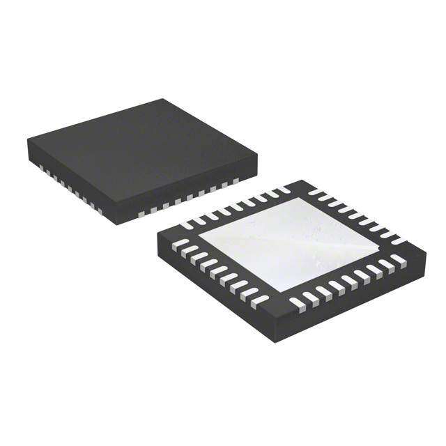
ICGOO电子元器件商城为您提供LTC5510IUF#PBF由LINEAR TECHNOLOGY设计生产,在icgoo商城现货销售,并且可以通过原厂、代理商等渠道进行代购。 LTC5510IUF#PBF价格参考。LINEAR TECHNOLOGYLTC5510IUF#PBF封装/规格:RF 混频器, RF Mixer IC General Purpose Up/Down Converter 1MHz ~ 6GHz 16-QFN (5x5)。您可以下载LTC5510IUF#PBF参考资料、Datasheet数据手册功能说明书,资料中有LTC5510IUF#PBF 详细功能的应用电路图电压和使用方法及教程。
LTC5510IUF#PBF是Linear Technology(现隶属于Analog Devices)推出的一款高性能射频(RF)混频器,属于无源双平衡混频器,采用紧凑的16引脚QFN封装。该器件主要工作频率范围为400MHz至2.5GHz,适用于高频无线通信系统中的上变频和下变频应用。

典型应用场景包括:蜂窝通信基础设施设备(如4G/LTE微基站、小型蜂窝基站)、点对点微波通信系统、软件定义无线电(SDR)、宽带无线接入系统以及工业与军事通信设备。由于其具备良好的线性度(高IIP3)和较低的本振(LO)驱动要求(仅需0dBm),LTC5510IUF#PBF在需要高动态性能和低功耗的系统中表现优异。

此外,该混频器具有较宽的中频(IF)带宽,支持直流至1.8GHz输出,适合零中频(Zero-IF)和低中频接收机架构。其良好的端口隔离性和稳定的温度特性也使其适用于环境复杂或可靠性要求较高的工业级应用。

综上,LTC5510IUF#PBF广泛应用于高性能无线通信系统中,尤其适合对灵敏度、线性度和集成度有较高要求的现代射频设计。
| 参数 | 数值 |
| 产品目录 | |
| 描述 | HIGH LINEARITY MIXER 16QFN |
| 产品分类 | |
| 品牌 | Linear Technology |
| 数据手册 | http://www.linear.com/docs/43381 |
| 产品图片 |
|
| 产品型号 | LTC5510IUF#PBF |
| RF类型 | 通用 |
| rohs | 无铅 / 符合限制有害物质指令(RoHS)规范要求 |
| 产品系列 | - |
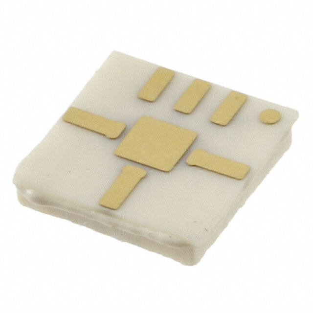
| 供应商器件封装 | 16-QFN(4x4) |
| 包装 | 管件 |
| 噪声系数 | 11.6dB |
| 增益 | 1.5dB |
| 封装/外壳 | 16-WQFN 裸露焊盘 |
| 标准包装 | 91 |
| 混频器数 | 1 |
| 电压-电源 | 3.1 V ~ 5.3 V |
| 电流-电源 | 105mA |
| 辅助属性 | 升/降频器 |
| 配用 | /product-detail/zh/DC1984A/DC1984A-ND/4890585/product-detail/zh/DC1983A/DC1983A-ND/4890581 |
| 频率 | 1MHz ~ 6GHz |


- 商务部:美国ITC正式对集成电路等产品启动337调查
- 曝三星4nm工艺存在良率问题 高通将骁龙8 Gen1或转产台积电
- 太阳诱电将投资9.5亿元在常州建新厂生产MLCC 预计2023年完工
- 英特尔发布欧洲新工厂建设计划 深化IDM 2.0 战略
- 台积电先进制程称霸业界 有大客户加持明年业绩稳了
- 达到5530亿美元!SIA预计今年全球半导体销售额将创下新高
- 英特尔拟将自动驾驶子公司Mobileye上市 估值或超500亿美元
- 三星加码芯片和SET,合并消费电子和移动部门,撤换高东真等 CEO
- 三星电子宣布重大人事变动 还合并消费电子和移动部门
- 海关总署:前11个月进口集成电路产品价值2.52万亿元 增长14.8%


PDF Datasheet 数据手册内容提取
LTC5510 1MHz to 6GHz Wideband High Linearity Active Mixer FEATURES DESCRIPTION n Input Frequency Range to 6GHz The LTC®5510 is a high linearity mixer optimized for applica- n 50Ω Matched Input from 30MHz to >3GHz tions requiring very wide input bandwidth, low distortion, n Capable of Up- or Down-Conversion and low LO leakage. The chip includes a double-balanced n OIP3: 27dBm at f = 1575MHz active mixer with an input buffer and a high speed LO ampli- OUT n 1.5dB Conversion Gain fier. The input is optimized for use with 1:1 transmission- n Noise Figure: 11.6dB at f = 1575MHz line baluns, allowing very wideband impedance matching. OUT n High Input P1dB: 11dBm at 5V The mixer can be used for both up- and down-conversion n 5V or 3.3V Supply at 105mA and can be used in wideband systems. n Shutdown Control The LO can be driven differentially or single-ended and n LO Input Impedance Always Matched requires only 0dBm of LO power to achieve excellent distor- n 0dBm LO Drive Level tion and noise performance, while also reducing external n 0n-Chip Temperature Monitor drive circuit requirements. The LTC5510 offers low LO n –40°C to 105°C Operation (T ) C leakage, greatly reducing the need for output filtering to n 16-Lead (4mm × 4mm) QFN Package meet LO suppression requirements. APPLICATIONS The LTC5510 is optimized for 5V but can also be used with a 3.3V supply with slightly reduced performance. n Wideband Receivers/Transmitters The shutdown function allows the part to be disabled for n Cable Downlink Infrastructure further power savings. n HF/VHF/UHF Mixer n Wireless Infrastructure L, LT, LTC, LTM, Linear Technology and the Linear logo are registered trademarks of Linear Technology Corporation. All other trademarks are the property of their respective owners. TYPICAL APPLICATION Conversion Gain, IIP3 and NF 30MHz to 4GHz Up/Down Mixer for Wideband Receiver vs Input Frequency LO 30 50Ω 0.1µF 0.1µF 30MH4zG THINOz TEMPMETROCANMTIUT11O:-R14RE3X+ 0.6pF00..11µµFF TINE+MPLTC551L0O+ LOO–UT+ 6.B8DnH1222J45:102006A.8HpFF O1550U7ΩT5MHz P3 (dBm), NF (dB)221055 IINPF3 HS LO LS LO 50Ω ILNG–ND BIAS OUT– 6.8nH AIN (dB), II10 fPOINU T= = – 11507d5BMmHz EN EN VCC1 VCC2 IADJ 4.75kΩ 10nF G 5 GC PTCL O= =2 50°dCBm 0 10nF 5V 0 1000 2000 3000 4000 1µF INPUT FREQUENCY (MHz) 5510 TA01a 5510 TA01 5510fa 1 For more information www.linear.com/LTC5510
LTC5510 ABSOLUTE MAXIMUM RATINGS PIN CONFIGURATION (Note 1) Supply Voltage (V , V , OUT+, OUT–) ................6.0V TOP VIEW CC1 CC2 Enable Voltage (EN) .........................–0.3V to VCC + 0.3V TP+LO–LO GND Current Adjust Voltage (I ) ....................–0.3V to 2.7V 16 15 14 13 ADJ TEMP 1 12 GND LO Input Power (1MHz to 6GHz) ........................+10dBm IN+ 2 11 OUT+ LO Differential DC Voltage .......................................1.5V 17 IN– 3 10 OUT– LO+, LO– Input DC Voltage ...........................–0.3V to 3V LGND 4 9 GND IN+, IN– Input Power (1MHz to 6GHz) ................+15dBm 5 6 7 8 IN+, IN– Input DC Voltage .........................–0.3V to 2.4V EN CC1 CC2 ADJ V V I Temp Monitor Input Current (TEMP) ......................10mA UF PACKAGE Operating Temperature Range (T ) ........–40°C to 105°C 16-LEAD (4mm × 4mm) PLASTIC QFN C Storage Temperature Range ..................–65°C to 150°C EXPOSED PAD (PTINJM 1A7X) =I S1 5G0N°DC,, MθJUC S=T 6 B°EC /SWO LDERED TO PCB Junction Temperature (T ) ....................................150°C J ORDER INFORMATION LEAD FREE FINISH TAPE AND REEL PART MARKING PACKAGE DESCRIPTION TEMPERATURE RANGE LTC5510IUF#PBF LTC5510IUF#TRPBF 5510 16-Lead (4mm × 4mm) Plastic QFN –40°C to 105°C Consult LTC Marketing for parts specified with wider operating temperature ranges. For more information on lead free part marking, go to: http://www.linear.com/leadfree/ For more information on tape and reel specifications, go to: http://www.linear.com/tapeandreel/ AC ELECTRICAL CHARACTERISTICS The l denotes the specifications which apply over the full operating temperature range, otherwise specifications are at T = 25°C. EN = High, P = 0dBm. Test circuit shown in Figure 1. (Notes 2, 3, 4) C LO PARAMETER CONDITIONS MIN TYP MAX UNITS Input Frequency Range Requires External Matching l 1 to 6000 MHz LO Input Frequency Range l 1 to 6500 MHz Output Frequency Range Requires External Matching l 1 to 6000 MHz Input Return Loss Z = 50Ω, 30MHz to 3GHz >11 dB O LO Input Return Loss Z = 50Ω, 1MHz to 5GHz >10 dB O Output Impedance Differential at 1500MHz 201Ω||0.6pF R||C LO Input Power f = 1MHz to 5GHz –6 0 6 dBm LO 5V Wideband Up/Downmixer Application: f = 30MHz to 3000MHz, f = 1575MHz, V = 5V, R1 = 4.75kΩ IN OUT CC Conversion Gain f = 190MHz, f = 1765MHz, Upmixer 0.5 1.5 dB IN LO f = 900MHz, f = 2475MHz, Upmixer 1.4 dB IN LO f = 2150MHz, f = 575MHz, Downmixer 1.1 dB IN LO f = 2600MHz, f = 1025MHz, Downmixer 1.2 dB IN LO Conversion Gain vs Temperature T = –40°C to 105°C, f = 900MHz l –0.007 dB/°C C IN 5510fa 2 For more information www.linear.com/LTC5510
LTC5510 AC ELECTRICAL CHARACTERISTICS The l denotes the specifications which apply over the full operating temperature range, otherwise specifications are at T = 25°C. EN = High, P = 0dBm, P = –10dBm (–10dBm/tone for two-tone tests), C LO IN unless otherwise noted. Test circuit shown in Figure 1. (Notes 2, 3, 4) PARAMETER CONDITIONS MIN TYP MAX UNITS Two-Tone Output 3rd Order Intercept f = 190MHz, f = 1765MHz, Upmixer 24.0 27.8 dBm IN LO (Δf = 2MHz) f = 900MHz, f = 2475MHz, Upmixer 25.0 dBm IN LO f = 2150MHz, f = 575MHz, Downmixer 26.0 dBm IN LO f = 2600MHz, f = 1025MHz, Downmixer 24.5 dBm IN LO SSB Noise Figure f = 190MHz, f = 1765MHz, Upmixer 11.6 14.5 dB IN LO f = 900MHz, f = 2475MHz, Upmixer 12.1 dB IN LO f = 2150MHz, f = 575MHz, Downmixer 11.6 dB IN LO f = 2600MHz, f = 1025MHz, Downmixer 11.8 dB IN LO SSB Noise Figure Under Blocking f =900MHz, f = 2475MHz, 20.3 dB IN LO f = 800MHz, P = +5dBm BLOCK BLOCK LO-IN Leakage f = 20MHz to 3300MHz <–50 dBm LO LO-OUT Leakage f = 20MHz to 1000MHz <–40 dBm LO f = 1000MHz to 3300MHz <–33 dBm LO IN-OUT Isolation f = 20MHz to 1150MHz >40 dB IN f = 1150MHz to 3000MHz >22 dB IN IN-LO Isolation f = 30MHz to 3000MHz >55 dB IN Input 1dB Compression f = 190MHz, f = 1765MHz, Upmixer 11.0 dBm IN LO f = 900MHz, f = 2475MHz, Upmixer 12.2 dBm IN LO f = 2150MHz, f = 575MHz, Downmixer 11.5 dBm IN LO f = 2600MHz, f = 1025MHz, Downmixer 11.6 dBm IN LO 3.3V Wideband Up/Downmixer Application: f = 30MHz to 3000MHz, f = 1575MHz, V = 3.3V, R1 = 1.8kΩ IN OUT CC Conversion Gain f = 190MHz, f = 1765MHz, Upmixer 1.5 dB IN LO f = 900MHz, f = 2475MHz, Upmixer 1.4 dB IN LO f = 2150MHz, f = 575MHz, Downmixer 1.1 dB IN LO f = 2600MHz, f = 1025MHz, Downmixer 1.2 dB IN LO Conversion Gain vs Temperature T = –40°C to 105°C, f = 900MHz l –0.006 dB/°C C IN Two-Tone Output 3rd Order Intercept f = 190MHz, f = 1765MHz, Upmixer 24.2 dBm IN LO (Δf = 2MHz) f = 900MHz, f = 2475MHz, Upmixer 23.3 dBm IN LO f = 2150MHz, f = 575MHz, Downmixer 23.9 dBm IN LO f = 2600MHz, f = 1025MHz, Downmixer 22.3 dBm IN LO SSB Noise Figure f = 190MHz, f = 1765MHz, Upmixer 11.2 dB IN LO f = 900MHz, f = 2475MHz, Upmixer 12.2 dB IN LO f = 2150MHz, f = 575MHz, Downmixer 11.4 dB IN LO f = 2600MHz, f = 1025MHz, Downmixer 11.4 dB IN LO SSB Noise Figure Under Blocking f = 900MHz, f = 2475MHz, 20.8 dB IN LO f = 800MHz P = +5dBm BLOCK BLOCK LO-IN Leakage f = 20MHz to 3300MHz <–50 dBm LO LO-OUT Leakage f = 20MHz to 1000MHz <–40 dBm LO f = 1000MHz to 3300MHz <–33 dBm LO IN-OUT Isolation f = 20MHz to 1150MHz >40 dB IN f = 1150MHz to 3000MHz >22 dB IN IN-LO Isolation f = 30MHz to 3000MHz >55 dB IN Input 1dB Compression f = 190MHz, f = 1765MHz, Upmixer 8.9 dBm IN LO f = 900MHz, f = 2475MHz, Upmixer 10.7 dBm IN LO f = 2150MHz, f = 575MHz, Downmixer 10.1 dBm IN LO f = 2600MHz, f = 1025MHz, Downmixer 9.6 dBm IN LO 5510fa 3 For more information www.linear.com/LTC5510
LTC5510 AC ELECTRICAL CHARACTERISTICS The l denotes the specifications which apply over the full operating temperature range, otherwise specifications are at T = 25°C. EN = High, P = 0dBm, P = –10dBm (–10dBm/tone for two-tone tests), C LO IN unless otherwise noted. Test circuit shown in Figure 1. (Notes 2, 3, 4) PARAMETER CONDITIONS MIN TYP MAX UNITS 5V Wideband Upmixer Application: f = 30MHz to 1000MHz, f = 2140MHz, f = f + f , V = 5V, R1 = 4.75kΩ IN OUT LO IN OUT CC Conversion Gain f = 190MHz 1.1 dB IN f = 450MHz 1.0 dB IN f = 900MHz 1.0 dB IN Conversion Gain vs Temperature T = –40°C to 105°C, f = 190MHz l –0.006 dB/°C C IN Two-Tone Output 3rd Order Intercept f = 190MHz 25.6 dBm IN (Δf = 2MHz) f = 450MHz 24.6 dBm IN f = 900MHz 23.9 dBm IN SSB Noise Figure f = 190MHz 12.0 dB IN f = 450MHz 12.2 dB IN f = 900MHz 12.4 dB IN SSB Noise Floor at P = +5dBm f = 800MHz, f = 3040MHz, f = 2140MHz –151.4 dBm/Hz IN IN LO OUT LO-IN Leakage f = 2100MHz to 3500MHz <–50 dBm LO LO-OUT Leakage f = 2100MHz to 3500MHz <–31 dBm LO IN-OUT Isolation f = 30MHz to 1100MHz >40 dB IN IN-LO Isolation f = 30MHz to 1100MHz >50 dB IN Input 1dB Compression f = 190MHz 11.5 dBm IN f = 450MHz 11.5 dBm IN f = 900MHz 11.7 dBm IN 5V VHF/UHF Wideband Downmixer Application: f = 100MHz to 1000MHz, f = 44MHz, f = f + f , V = 5V, R1 = Open IN OUT LO IN OUT CC Conversion Gain f = 140MHz 1.9 dB IN f = 456MHz 1.9 dB IN f = 900MHz 1.9 dB IN Conversion Gain vs Temperature T = –40°C to 105°C, f = 456MHz l –0.006 dB/°C C IN Two-Tone Input 3rd Order Intercept f = 140MHz 27.8 dBm IN (Δf = 2MHz) f = 456MHz 28.5 dBm IN f = 900MHz 26.8 dBm IN SSB Noise Figure f = 140MHz 10.8 dB IN f = 456MHz 10.9 dB IN f = 900MHz 11.6 dB IN SSB Noise Figure Under Blocking f = 900MHz, f = 944MHz, 20.0 dB IN LO f = 800MHz, P = +5dBm BLOCK BLOCK Two-Tone Input 2nd Order Intercept f = 477MHz, f = 435MHz, f = 500MHz 72 dBm IN1 IN2 LO (Δf = f = 42MHz) IM2 2LO-2RF Output Spurious Product f = 478MHz at –6dBm, f = 500MHz, f = 44MHz –84 dBc IN LO OUT (f = f – f /2) IN LO OUT 3LO-3RF Output Spurious Product f = 485.33MHz at –6dBm, f = 500MHz, –82 dBc IN LO (f = f – f /3) f = 44.01MHz IN LO OUT OUT LO-IN Leakage f = 50MHz to 1200MHz <–62 dBm LO LO-OUT Leakage f = 50MHz to 1200MHz <–31 dBm LO IN-OUT Isolation f = 50MHz to 1000MHz >23 dB IN IN-LO Isolation f = 50MHz to 1000MHz >62 dB IN Input 1dB Compression f = 456MHz 12.1 dBm IN 5510fa 4 For more information www.linear.com/LTC5510
LTC5510 AC ELECTRICAL CHARACTERISTICS The l denotes the specifications which apply over the full operating temperature range, otherwise specifications are at T = 25°C. EN = High, P = 0dBm, P = –10dBm (–10dBm/tone for two-tone tests), C LO IN unless otherwise noted. Test circuit shown in Figure 1. (Notes 2, 3, 4) PARAMETER CONDITIONS MIN TYP MAX UNITS 5V VHF/UHF Upmixer Application: f = 70MHz, f = 100MHz to 1000MHz, f = f + f , V = 5V, R1 = Open, L3 = 220nH IN OUT LO IN OUT CC Conversion Gain f = 456MHz 1.1 dB OUT Conversion Gain vs Temperature T = –40°C to 105°C, f = 456MHz l –0.007 dB/°C C OUT Two-Tone Output 3rd Order Intercept f = 456MHz 29.0 dBm OUT (Δf = 2MHz) SSB Noise Figure f = 456MHz 11.3 dB OUT SSB Noise Floor at P = +5dBm f = 44MHz, f = 532MHz, f = 462MHz –152 dBm/Hz IN IN LO OUT LO-IN Leakage f = 100MHz to 1500MHz <–62 dBm LO LO-OUT Leakage f = 100MHz to 1500MHz <–39 dBm LO IN-OUT Isolation f = 50MHz to 400MHz >43 dB IN IN-LO Isolation f = 50MHz to 400MHz >70 dB IN Input 1dB Compression f = 456MHz 11.0 dBm OUT DC ELECTRICAL CHARACTERISTICS The l denotes the specifications which apply over the full operating temperature range, otherwise specifications are at T = 25°C. V = 5V, EN = High, unless otherwise noted. Test circuit shown in C CC Figure 1. (Note 2) PARAMETER CONDITIONS MIN TYP MAX UNITS Power Supply Supply Voltage (Pins 6, 7, 10, 11) 5V Supply l 4.5 5 5.3 V 3.3V Supply l 3.1 3.3 3.5 V Supply Current (Pins 6, 7, 10, 11) 5V, R1 = Open 105 mA 5V, R1 = 4.75k 99.6 113 mA 3.3V, R1 = Open 105 mA 3.3V, R1 = 1.8k 94 mA Total Supply Current – Shutdown EN = Low 1.3 2.5 mA Enable Logic Input (EN) EN Input High Voltage (On) l 1.8 V EN Input Low Voltage (Off) l 0.5 V EN Input Current –0.3V to V + 0.3V –20 200 μA CC Turn-On Time EN: Low to High 0.6 μs Turn-Off Time EN: High to Low 0.6 μs Current Adjust Pin (I ) ADJ Open Circuit DC Voltage 1.8 V Short Circuit DC Current I Shorted to Ground 1.9 mA ADJ Temperature Monitor Pin (TEMP) DC Voltage at T = 25°C I = 10µA 697 mV J IN I = 80µA 755 mV IN Voltage Temperature Coefficient I = 10µA l –1.80 mV/°C IN I = 80µA l –1.61 mV/°C IN Note 1: Stresses beyond those listed under Absolute Maximum Ratings Note 3: SSB Noise Figure measured with a small-signal noise source, may cause permanent damage to the device. Exposure to any Absolute bandpass filter and 3dB matching pad on the signal input, bandpass filter Maximum Rating condition for extended periods may affect device and 6dB matching pad on the LO input, and no other RF signals applied. reliability and lifetime. Note 4: Specified performance includes all external component and Note 2: The LTC5510 is guaranteed functional over the case operating evaluation PCB losses. temperature range of –40°C to 105°C. (θJC = 6°C/W) 5510fa 5 For more information www.linear.com/LTC5510
LTC5510 TYPICAL DC PERFORMANCE CHARACTERISTICS (Test Circuit Shown in Figure 1) 5V Supply Current 3.3V Supply Current vs Supply Voltage vs Supply Voltage 106 98 R1 = 4.75kΩ R1 = 1.8kΩ 104 TC = –40°C 96 mA) TC = –40°C mA) NT ( 102 NT ( 94 TC = 25°C E E R R UR 100 TC = 25°C UR C C LY LY 92 TC = 85°C UPP 98 TC = 85°C UPP S S 90 TC = 105°C 96 TC = 105°C 94 88 4.5 4.7 4.9 5.1 5.3 3.0 3.1 3.2 3.3 3.4 3.5 3.6 SUPPLY VOLTAGE (V) SUPPLY VOLTAGE (V) 5510 G01 5510 G02 TYPICAL AC PERFORMANCE CHARACTERISTICS 5V Wideband Up/Downmixer Application: V = 5V, T = 25°C, f = 190MHz, P = –10dBm (–10dBm/tone for 2-tone tests, Δf = 2MHz), f = 1765MHz, P = 0dBm, output CC C IN IN LO LO measured at 1575MHz, unless otherwise noted. (Test Circuit Shown in Figure 1). Conversion Gain Distribution Noise Figure Distribution at 1575MHz OIP3 Distribution at 1575MHz at 1575MHz 50 50 50 85°C fIN = 190MHz 85°C fIN = 190MHz 85°C fIN = 190MHz 25°C 25°C 25°C –40°C –40°C –40°C 40 40 40 %) %) %) N ( 30 N ( 30 N ( 30 O O O TI TI TI U U U B B B TRI 20 TRI 20 TRI 20 S S S DI DI DI 10 10 10 0 0 0 0.8 1 1.2 1.4 1.6 1.8 2 2.2 21 23 25 27 29 31 33 9 10 11 12 13 14 GAIN (dB) OIP3 (dBm) NOISE FIGURE (dB) 5510 G03 5510 G04 5510 G05 5510fa 6 For more information www.linear.com/LTC5510
LTC5510 TYPICAL AC PERFORMANCE CHARACTERISTICS 5V Wideband Up/Downmixer Application for f < 1575MHz: V = 5V, T = 25°C, f = 190MHz, P = –10dBm (–10dBm/tone for 2-tone tests, Δf = 2MHz), HSLO, IN CC C IN IN P = 0dBm, output measured at 1575MHz, unless otherwise noted. (Test Circuit Shown in Figure 1). LO Conversion Gain, OIP3 and NF Conversion Gain and OIP3 vs Input Frequency vs Output Frequency LO Leakage vs LO Frequency 32 32 0 28 OIP3 28 –10 B) OIP3 d N (dB), OIP3 (dBm), NF ( 221140628 NF TTTTCCCC ==== 182–05545°°0CC°°CC GAIN (dB), OIP3 (dBm) 221140628 TTTTCCCC ==== 182–05545°°0CC°°CC LO LEAKAGE (dBm) –––––2345600000 LOL-OOU-ITN AI G 4 GC 4 GC –70 0 0 –80 0 400 800 1200 1600 1200 1400 1600 1800 2000 1500 1900 2300 2700 3100 INPUT FREQUENCY (MHz) OUTPUT FREQUENCY (MHz) LO FREQUENCY (MHz) 5510 G06 5510 G07 5510 G08 Conversion Gain, OIP3 and NF Noise Figure Conversion Gain, OIP3 and NF vs LO Power vs Input Blocker Level vs Supply Voltage 32 24 32 fIN = 900MHz 28 fBLOCK = 800MHz 28 B) 22 fLO = 2475MHz B) d d OIP3 OIP3 (dBm), NF ( 221406 NOFIP3 TTTTCCCC ==== 182–05545°°0CC°°CC E FIGURE (dB) 2108 630–Pddd3LOBBBdB mmm=m –6dBm OIP3 (dBm), NF ( 221406 NF TTTTCCCC ==== 182–05545°°0CC°°CC B), 12 OIS 16 B), 12 d N d N ( 8 N ( 8 AI AI G 14 G 4 GC 4 GC 0 12 0 –12 –9 –6 –3 0 3 6 –20 –15 –10 –5 0 5 4.5 4.6 4.7 4.8 4.9 5.0 5.1 5.2 5.3 LO INPUT POWER (dBm) BLOCKER POWER (dBm) SUPPLY VOLTAGE (V) 5510 G09 5510 G10 5510 G11 IM3 Level IM2 Level Conversion Gain, OIP3, NF and vs Output Power (2-Tone) vs Output Power (2-Tone) Input P1dB vs Case Temperature 0 0 35 –20 TTTTCCCC ==== 182–05545°°0CC°°CC –20 TTTTCCCC ==== 182–05545°°0CC°°CC dB (dBm) 30 OIP3 P1 25 VEL (dBc) –40 VEL (dBc) –40 OIP3 AND 20 IM3 LE –60 IM2 LE –60 NF (dB), 1150 NF D IP1dB –80 –80 AN N 5 fIM2 = 1385MHz GAI GC –100 –100 0 –15 –10 –5 0 5 –15 –10 –5 0 5 –45 –15 15 45 75 105 OUTPUT POWER (dBm) OUTPUT POWER (dBm) CASE TEMPERATURE (°C) 5510 G12 5510 G13 5510 G14 5510fa 7 For more information www.linear.com/LTC5510
LTC5510 TYPICAL AC PERFORMANCE CHARACTERISTICS 5V Wideband Up/Downmixer Application for f > 1575MHz: V = 5V, T = 25°C, f = 2150MHz, P = –10dBm (–10dBm/tone for 2-tone tests, Δf = 2MHz), LSLO, P = 0dBm, IN CC C IN IN LO output measured at 1575MHz, unless otherwise noted. (Test Circuit Shown in Figure 1). Conversion Gain, OIP3 and NF Conversion Gain and OIP3 vs Input Frequency vs Output Frequency LO Leakage vs LO Frequency 30 30 0 OIP3 OIP3 –10 B) 25 25 d N (dB), OIP3 (dBm), NF ( 211050 NF TTTTCCCC ==== 182–05545°°0CC°°CC GAIN (dB), OIP3 (dBm) 211050 TTTTCCCC ==== 182–05545°°0CC°°CC LO LEAKAGE (dBm) –––––2345600000 LO-OUT LO-IN AI G 5 5 –70 GC GC 0 0 –80 1600 2000 2400 2800 3200 1200 1400 1600 1800 2000 0 300 600 900 1200 1500 INPUT FREQUENCY (MHz) OUTPUT FREQUENCY (MHz) LO FREQUENCY (MHz) 5510 G15 5510 G16 5510 G17 Conversion Gain, OIP3 and NF Conversion Gain, OIP3 and NF vs LO Power vs Supply Voltage 30 30 B) 25 B) 25 F (d OIP3 TC = 105°C F (d OIP3 TC = 105°C m), N 20 TTCC == 8255°°CC m), N 20 TTCC == 8255°°CC 3 (dB 15 NF TC = –40°C 3 (dB 15 TC = –40°C P P OI OI B), 10 B), 10 d d N ( N ( NF AI AI G 5 G 5 GC GC 0 0 –12 –9 –6 –3 0 3 6 4.5 4.7 4.9 5.1 5.3 LO INPUT POWER (dBm) SUPPLY VOLTAGE (V) 5510 G18 5510 G20 IM3 Level Conversion Gain, OIP3, NF and vs Output Power (2-Tone) Input P1dB vs Case Temperature 0 30 TTCC == 18055°C°C Bm) –20 TTCC == 2–54°0C°C dB (d 25 OIP3 1 P dBc) –40 AND 20 VEL ( OIP3 15 NF IM3 LE –60 NF (dB), 10 IP1dB D –80 N AN 5 AI GC G –100 0 –15 –10 –5 0 5 –45 –15 15 45 75 105 OUTPUT POWER (dBm) CASE TEMPERATURE (°C) 5510 G21 5510 G23 5510fa 8 For more information www.linear.com/LTC5510
LTC5510 TYPICAL AC PERFORMANCE CHARACTERISTICS 3.3V Wideband Up/Downmixer Application for f < 1575MHz: V = 3.3V, T = 25°C, f = 190MHz, P = –10dBm (–10dBm/tone for 2-tone tests, Δf = 2MHz), HSLO, P = 0dBm, IN CC C IN IN LO output measured at 1575MHz, unless otherwise noted. (Test Circuit Shown in Figure 1). Conversion Gain, OIP3 and NF Conversion Gain and OIP3 vs Input Frequency vs Output Frequency LO Leakage vs LO Frequency 32 35 0 28 30 –10 B) d AIN (dB), OIP3 (dBm), NF ( 221140628 NF OIP3 TTCC == 18055°C°C GAIN (dB), OIP3 (dBm) 22115050 OIP3 TTTTCCCC ==== 182–05545°°0CC°°CC LO LEAKAGE (dBm) –––––2345600000 LOL-OOU-ITN G 4 GC TTCC == 2–54°0C°C 5 GC –70 0 0 –80 0 400 800 1200 1600 1200 1400 1600 1800 2000 1500 1900 2300 2700 3100 INPUT FREQUENCY (MHz) OUTPUT FREQUENCY (MHz) LO FREQUENCY (MHz) 5510 G24 5510 G25 5510 G26 Conversion Gain, OIP3 and NF Noise Figure Conversion Gain, OIP3 and NF vs LO Power vs Input Blocker Level vs Supply Voltage 32 24 32 fIN = 900MHz 28 fBLOCK = 800MHz 28 B) 22 fLO = 2475MHz B) OIP3 d d OIP3 (dBm), NF ( 221406 ONIFP3 TTTTCCCC ==== 182–05545°°0CC°°CC E FIGURE (dB) 2108 630–Pddd3LOBBBdB mmm=m –6dBm OIP3 (dBm), NF ( 221406 TTTTCCCC ==== 182–05545°°0CC°°CC NF N (dB), 128 NOIS 16 N (dB), 128 AI AI G 14 G 4 GC 4 GC 0 12 0 –12 –9 –6 –3 0 3 6 –20 –15 –10 –5 0 5 3.0 3.1 3.2 3.3 3.4 3.5 3.6 LO INPUT POWER (dBm) BLOCKER POWER (dBm) SUPPLY VOLTAGE (V) 5510 G27 5510 G28 5510 G29 IM3 Level IM2 Level Conversion Gain, OIP3, NF and vs Output Power (2-Tone) vs Output Power (2-Tone) Input P1dB vs Case Temperature 0 0 35 –20 TTTTCCCC ==== 182–05545°°0CC°°CC –20 TTTTCCCC ==== 182–05545°°0CC°°CC dB (dBm) 30 OIP3 P1 25 VEL (dBc) –40 VEL (dBc) –40 OIP3 AND 20 IM3 LE –60 IM2 LE –60 NF (dB), 1150 NF D –80 –80 AN IP1dB N 5 fIM2 = 1385MHz GAI GC –100 –100 0 –15 –10 –5 0 5 –15 –10 –5 0 5 –45 –15 15 45 75 105 OUTPUT POWER (dBm) OUTPUT POWER (dBm) CASE TEMPERATURE (°C) 5510 G30 5510 G31 5510 G32 5510fa 9 For more information www.linear.com/LTC5510
LTC5510 TYPICAL AC PERFORMANCE CHARACTERISTICS 3.3V Wideband Up/Downmixer Application for f > 1575MHz: V = 3.3V, T = 25°C, f = 2150MHz, P = –10dBm (–10dBm/tone for 2-tone tests, Δf = 2MHz), LSLO, P = 0dBm, IN CC C IN IN LO output measured at 1575MHz, unless otherwise noted. (Test Circuit Shown in Figure 1). Conversion Gain, OIP3 and NF Conversion Gain and OIP3 vs Input Frequency vs Output Frequency LO Leakage vs LO Frequency 30 30 0 OIP3 –10 B) 25 25 d AIN (dB), OIP3 (dBm), NF ( 211050 NFOIP3 TTCC == 18055°C°C GAIN (dB), OIP3 (dBm) 211050 TTTTCCCC ==== 182–05545°°0CC°°CC LO LEAKAGE (dBm) –––––2345600000 LO-OUT G 5 TC = 25°C 5 LO-IN GC TC = –40°C GC –70 0 0 –80 1600 2000 2400 2800 3200 1200 1400 1600 1800 2000 0 300 600 900 1200 1500 INPUT FREQUENCY (MHz) OUTPUT FREQUENCY (MHz) LO FREQUENCY (MHz) 5510 G33 5510 G34 5510 G35 Conversion Gain, OIP3 and NF Conversion Gain, OIP3 and NF vs LO Power vs Supply Voltage 30 30 OIP3 B) 25 B) 25 d d F ( F ( P3 (dBm), N 2105 OIP3 TTTTCCCC ==== 182–05545°°0CC°°CC P3 (dBm), N 2105 NF TTTTCCCC ==== 182–05545°°0CC°°CC OI OI dB), 10 NF dB), 10 N ( N ( AI AI G 5 G 5 GC GC 0 0 –12 –9 –6 –3 0 3 6 3.0 3.1 3.2 3.3 3.4 3.5 3.6 LO INPUT POWER (dBm) SUPPLY VOLTAGE (V) 5510 G36 5510 G38 IM3 Level Conversion Gain, OIP3, NF and vs Output Power (2-Tone) Input P1dB vs Case Temperature 0 30 TC = 105°C m) TC = 85°C B –20 TTCC == 2–54°0C°C 1dB (d 25 OIP3 P Bc) ND 20 d A VEL ( –40 OIP3 15 IM3 LE NF (dB), 10 IPN1FdB –60 D N N A 5 GAI GC –80 0 –15 –10 –5 0 5 –45 –15 15 45 75 105 OUTPUT POWER (dBm) CASE TEMPERATURE (°C) 5510 G39 5510 G41 5510fa 10 For more information www.linear.com/LTC5510
LTC5510 TYPICAL AC PERFORMANCE CHARACTERISTICS 5V Wideband Upmixer Application: V = 5V, T = 25°C, f = 190MHz, P = –10dBm (–10dBm/tone for 2-tone tests, Δf = 2MHz), HSLO, P = 0dBm, output measured at CC C IN IN LO 2140MHz, unless otherwise noted. (Test Circuit Shown in Figure 1). Conversion Gain, OIP3 and NF Conversion Gain, OIP3 and NF vs Input Frequency vs Output Frequency LO Leakage vs LO Frequency 32 32 0 OIP3 28 28 –10 B) B) d d OIP3 F ( 24 F ( 24 –20 dBm), N 20 TTTCCC === 1820555°°CC°C dBm), N 20 TTTCCC === 1820555°°CC°C E (dBm) –30 LO-OUT P3 ( 16 TC = –40°C P3 ( 16 NF TC = –40°C KAG –40 N (dB), OI 128 NF N (dB), OI 128 LO LEA ––5600 GAI GAI LO-IN 4 4 –70 GC GC 0 0 –80 0 400 800 1200 1600 1700 1800 1900 2000 2100 2200 2300 2100 2300 2500 2700 2900 3100 3300 3500 INPUT FREQUENCY (MHz) OUTPUT FREQUENCY (MHz) LO FREQUENCY (MHz) 5510 G42 5510 G43 5510 G44 Conversion Gain, OIP3 and NF Conversion Gain, OIP3 and NF vs LO Power Output Noise Floor vs Input Power vs Supply Voltage 32 –146 32 fIN = 800MHz 28 –148 fLO = 3040MHz 28 B) B) AIN (dB), OIP3 (dBm), NF (d 221140628 NOFIP3 TTTTCCCC ==== 182–05545°°0CC°°CC OUTPUT NOISE (dBm/Hz) –––––111115555502468 630–Pddd3LOBBBdB mmm=m –6dBm AIN (dB), OIP3 (dBm), NF (d 221140628 ONIFP3 TTTTCCCC ==== 182–05545°°0CC°°CC G G 4 –160 4 GC GC 0 –162 0 –12 –9 –6 –3 0 3 6 –20 –15 –10 –5 0 5 4.5 4.6 4.7 4.8 4.9 5.0 5.1 5.2 5.3 LO INPUT POWER (dBm) INPUT POWER (dBm) SUPPLY VOLTAGE (V) 5510 G45 5510 G46 5510 G47 IM3 Level IM2 Level Conversion Gain, OIP3, NF and vs Output Power (2-Tone) vs Output Power (2-Tone) Input P1dB vs Case Temperature 0 0 30 TTCC == 18055°C°C TTCC == 18055°C°C Bm) OIP3 –20 TTCC == 2–54°0C°C –20 TTCC == 2–54°0C°C dB (d 25 1 P dBc) –40 dBc) –40 AND 20 VEL ( VEL ( OIP3 15 NF IM3 LE –60 IM2 LE –60 NF (dB), 10 IP1dB D –80 –80 N AN 5 fIM2 = 1950MHz GAI GC –100 –100 0 –15 –10 –5 0 5 –15 –10 –5 0 5 –45 –15 15 45 75 105 OUTPUT POWER (dBm) OUTPUT POWER (dBm) CASE TEMPERATURE (°C) 5510 G48 5510 G49 5510 G50 5510fa 11 For more information www.linear.com/LTC5510
LTC5510 TYPICAL AC PERFORMANCE CHARACTERISTICS 5V VHF/UHF Upmixer Application: V = 5V, T = 25°C, f = 70MHz, P = –10dBm (–10dBm/tone for 2-tone tests, Δf = 2MHz), HSLO, P = 0dBm, output measured at CC C IN IN LO 456MHz, unless otherwise noted. (Test Circuit Shown in Figure 2). Conversion Gain, OIP3 and NF Conversion Gain and OIP3 vs Output Frequency vs Input Frequency LO Leakage vs LO Frequency 32 32 0 OIP3 28 28 –10 B) OIP3 d –20 N (dB), OIP3 (dBm), NF ( 221140628 NF TTTTCCCC ==== 182–05545°°0CC°°CC GAIN (dB), OIP3 (dBm) 221140628 TTTTCCCC ==== 182–05545°°0CC°°CC LO LEAKAGE (dBm) ––––34560000 LLOO-O-IUNT AI –70 G 4 GC 4 GC –80 0 0 –90 0 200 400 600 800 1000 0 100 200 300 400 0 300 600 900 1200 1500 OUTPUT FREQUENCY (MHz) INPUT FREQUENCY (MHz) LO FREQUENCY (MHz) 5510 G51 5510 G52 5510 G53 Conversion Gain, OIP3 and NF Output Noise Floor Conversion Gain, OIP3 and NF vs LO Power vs Input Power vs Supply Voltage 32 –146 32 fIN = 44MHz 28 –148 fOUT = 462MHz 28 B) OIP3 fLO = 532MHz B) OIP3 AIN (dB), OIP3 (dBm), NF (d 221140628 NF TTTTCCCC ==== 182–05545°°0CC°°CC OUTPUT NOISE (dBm/Hz)–––––111115555502468 630–Pddd3LOBBBdB mmm=m –6dBm AIN (dB), OIP3 (dBm), NF (d 221140628 NF TTTTCCCC ==== 182–05545°°0CC°°CC G G 4 –160 4 GC GC 0 –162 0 –12 –9 –6 –3 0 3 6 –20 –15 –10 –5 0 5 4.5 4.6 4.7 4.8 4.9 5.0 5.1 5.2 5.3 LO INPUT POWER (dBm) INPUT POWER (dBm) SUPPLY VOLTAGE (V) 5510 G54 5510 G55 5510 G56 IM3 Level IM2 Level Conversion Gain, OIP3, NF and vs Output Power (2-Tone) vs Output Power (2-Tone) Input P1dB vs Case Temperature 0 0 32 TTCC == 18055°C°C TTCC == 18055°C°C Bm) 28 OIP3 –20 TTCC == 2–54°0C°C –20 TTCC == 2–54°0C°C 1dB (d 24 P D N 20 IM3 (dBc) ––4600 IM2 (dBc) ––4600 dB), OIP3 A 1162 IP1dB F ( N D 8 NF –80 –80 AN fIM2 = 386MHz GAIN 4 GC –100 –100 0 –15 –12 –9 –6 –3 0 3 6 –15 –12 –9 –6 –3 0 3 6 –45 –15 15 45 75 105 OUTPUT POWER (dBm) OUTPUT POWER (dBm) CASE TEMPERATURE (°C) 5510 G57 5510 G58 5510 G59 5510fa 12 For more information www.linear.com/LTC5510
LTC5510 TYPICAL AC PERFORMANCE CHARACTERISTICS 5V VHF/UHF Downmixer Application: V = 5V, T = 25°C, f = 456MHz, P = –10dBm (–10dBm/tone for 2-tone tests, Δf = 2MHz), HSLO, P = 0dBm, output measured at CC C IN IN LO 44MHz, unless otherwise noted. (Test Circuit Shown in Figure 2). Conversion Gain, IIP3 and NF Conversion Gain and IIP3 vs Input Frequency vs Output Frequency LO Leakage vs LO Frequency 30 30 0 IIP3 –10 B) 25 IIP3 25 AIN (dB), IIP3 (dBm), NF (d 211050 NF TTTTCCCC ==== 182–05545°°0CC°°CC GAIN (dB), IIP3 (dBm) 121005 TTTTCCCC ==== 182–05545°°0CC°°CC LO LEAKAGE (dBm) –––––2345600000 LO-OUT G 5 5 LO-IN GC GC –70 0 0 –80 0 200 400 600 800 1000 0 50 100 150 200 250 300 0 200 400 600 800 1000 1200 INPUT FREQUENCY (MHz) OUTPUT FREQUENCY (MHz) LO FREQUENCY (MHz) 5510 G60 5510 G61 5510 G62 Conversion Gain, IIP3 and NF Noise Figure Conversion Gain, IIP3 and NF vs LO Power vs Input Blocker Level vs Supply Voltage 30 26 30 PLO = –6dBm IIP3 PLO = –3dBm IIP3 N (dB), IIP3 (dBm), NF (dB) 22115050 NF TTTTCCCC ==== 182–05545°°0CC°°CC NOISE FIGURE (dB) 2221142086 fffIBLNOL O ==C 9K90 4=0PPP4 M8MLLL0OOOHH0 z===zM 036HdddzBBBmmm N (dB), IIP3 (dBm), NF (dB) 22115050 NF TTTTCCCC ==== 182–05545°°0CC°°CC AI AI G 5 G 5 GC 14 GC 0 12 0 –12 –9 –6 –3 0 3 6 –20 –15 –10 –5 0 5 4.5 4.6 4.7 4.8 4.9 5.0 5.1 5.2 5.3 LO INPUT POWER (dBm) BLOCKER POWER (dBm) SUPPLY VOLTAGE (V) 5510 G63 5510 G64 5510 G65 IM3 Level Conversion Gain, IIP3, NF and vs Input Power (2-Tone) Input P1dB vs Case Temperature 0 30 TTCC == 18055°C°C Bm) IIP3 –20 TTCC == 2–54°0C°C dB (d 25 1 P D 20 Bc) –40 3 AN IM3 (d –60 dB), IIP 15 IP1dB F ( 10 D N NF N –80 A AIN 5 GC G –100 0 –15 –10 –5 0 5 –45 –15 15 45 75 105 INPUT POWER (dBm) CASE TEMPERATURE (°C) 5510 G66 5510 G68 5510fa 13 For more information www.linear.com/LTC5510
LTC5510 PIN FUNCTIONS TEMP (Pin 1): Temperature Monitor. This pin is connected I (Pin 8): Bias Adjust Pin. This pin allows adjustment ADJ to the anode of a diode through a 30Ω resistor. It may be of the internal mixer current by adding an external pull- used to measure the die temperature by forcing a current down resistor. The typical DC voltage on this pin is 1.8V. into the pin and measuring the voltage. If not used, this pin must be left floating. IN+, IN– (Pins 2, 3): Differential Signal Input. For optimum GND (Pins 9, 12, 13, Exposed Pad (Pin 17)): Ground. performance, these pins should be driven with a differential These pins must be soldered to the RF ground plane on signal. The input can be driven single-ended, with some the circuit board. The exposed metal pad of the package performance degradation, by connecting the undriven pin provides both electrical contact to ground and a good to RF ground through a capacitor. An internally generated thermal contact to the printed circuit board. 1.6V DC bias voltage is present on these pins, thus DC OUT–, OUT+ (Pins 10, 11,): Differential Output. These blocking capacitors are required. pins must be connected to a DC supply through imped- LGND (Pin 4): DC Ground Return for the Input Amplifier. ance matching inductors and/or a transformer center-tap. This pin must be connected to DC ground. The typical Typical DC current consumption is 32mA into each pin. current from this pin is 64mA. In some applications an LO–, LO+ (Pins 14, 15): Differential Local Oscillator Input. external chip inductor may be used. Note that any induc- A single-ended LO may be used by connecting one pin to tor DC resistance will reduce the current through this pin. RF ground through a DC blocking capacitor. These pins EN (Pin 5): Enable Pin. When the applied voltage is greater are internally biased to 1.7V; thus, DC blocking capacitors than 1.8V, the IC is enabled. Below 0.5V, the IC is disabled. are required. Each LO input pin is internally matched to 50Ω for both EN states. V , V (Pins 6, 7): Power Supply Pins for the Bias CC1 CC2 and LO Buffer Circuits. Typical current consumption is TP (Pin 16): Test Pin. This pin is used for production test 41mA. These pins should be connected together on the purposes only and must be connected to ground. circuit board and decoupled with a 10nF capacitor located close to the pins. BLOCK DIAGRAM EXPOSED PAD GND TP LO+ LO– GND 17 16 15 14 13 TEMP 1 12 GND IN+ 2 11 OUT+ 10 OUT– IN– 3 9 GND BIAS LGND 4 5 6 7 8 EN VCC1 VCC2 IADJ 5510 BD 5510fa 14 For more information www.linear.com/LTC5510
LTC5510 TEST CIRCUITS LO RF 50Ω 0.015” GND DC1983A C4 C5 0.062” EVALUATION BOARD BIAS STACK-UP 0.015” GND (NELCO N4000-13) 16 15 14 13 TP LO+ LO– GND TO VCC TEMPERATURE 1 TEMP GND 12 C8 MONITOR LTC5510 T1 C1 C9 1:1 2 IN+ OUT+ 11 L1 OUT IN 3 4 50Ω 50Ω 1 6 C3 17 T2 3 2 1 C2 GND 4:1 3 IN– OUT– 10 L2 4 5 6 NC 4 LGND GND 9 EN VCC1 VCC2 IADJ L3 5 6 7 8 R1 EN VCC C7 C6 5510 F01 5V/3.3V Wideband Up/Downmixer* 5V Wideband Upmixer f = 30MHz-3000MHz f = 30MHz-2500 MHz IN IN REF DES f = 1575MHz f = 2140MHz SIZE COMMENTS OUT OUT C1, C2, C4, C5 0.1µF 0.1µF 0402 Murata GRM15, X7R C3 0.7pF - 0402 Murata GJM15, C0G C6 1µF 1µF 0603 Murata GRM18, X7R C7, C8 10nF 10nF 0402 Murata GRM15, X7R C9 6.8pF 5.6pF 0402 Murata GJM15, C0G L1, L2 6.8nH 5.6nH 0402 CoilCraft 0402HP L3 0Ω 0Ω 0603 R1 4.75kΩ (5V), 4.75kΩ 0402 1% 1.8kΩ (3.3V) T1 Mini-Circuits Mini-Circuits TC1-1-13M+ TC1-1-13M+ T2 Anaren Mini-Circuits BD1222J50200AHF NCS4-232+ *Standard DC1983A Eval Board Configuration Figure 1. High Frequency Output Test Circuit Schematic (DC1983A) 5510fa 15 For more information www.linear.com/LTC5510
LTC5510 TEST CIRCUITS LO 50Ω 0.015” RF GND DC1984A C4 C5 0.062” EVALUATION BOARD BIAS STACK-UP 0.015” GND (NELCO N4000-13) 16 15 14 13 TP LO+ LO– GND TEMPERATURE 1 TEMP GND 12 MONITOR L4 LTC5510 T2 T1 C1 4:1 C9 1:1 2 IN+ OUT+ 11 L1 3 4 OUT+ IN 3 4 17 50Ω 1 6 C3C2 GND 2 C10 3 IN– OUT– 10 L2 C8 1 6 OUT– L5 OPTIONAL 4 LGND GND 9 DIFF OUT EN VCC1 VCC2 IADJ L3 5 6 7 8 R1 EN VCC C7 C6 5510 F02 5V VHF/UHF 5V VHF/UHF Upmixer* Wideband Downmixer f = 70MHz f = 100MHz-1000 MHz IN IN REF DES f = 100MHz-1000 MHz f = 44MHz SIZE COMMENTS OUT OUT C1, C2, C4, C5 0.1µF 0.1µF 0402 Murata GRM15, X7R C3 0.5pF 0.9pF 0402 Murata GJM15, C0G C6 1µF 1µF 0603 Murata GRM18, X7R C7, C8, C9, C10 10nF 10nF 0402 Murata GRM15, X7R L1, L2 - - 0603 L3 220nH 0Ω 0603 Coilcraft 0603HP, WE 744761 L4, L5 15nH 0Ω 0402 CoilCraft 0402HP R1 - - 0402 T1 Mini-Circuits Mini-Circuits TC1-1-13M+ TC1-1-13M+ T2 Mini-Circuits Mini-Circuits TC4-19LN+ TC4-1W-7ALN+ *Standard DC1984A Eval Board Configuration Figure 2. Low Frequency Output Test Circuit Schematic (DC1984A) 5510fa 16 For more information www.linear.com/LTC5510
LTC5510 APPLICATIONS INFORMATION The LTC5510 uses wideband high performance RF and LO external components required for the data sheet specified amplifiers driving a double-balanced mixer core to achieve performance are shown in Figures 1 and 2. The evaluation frequency up- or down-conversion with high linearity over boards are shown in Figures 3a and 3b. a very broad frequency range. For flexibility, all ports are The High Frequency Output test circuit, shown in Figure 1, differential; however, the LO port has also been optimized utilizes a multilayer chip balun to realize a single-ended for single-ended use. Low side or high side LO injection output. The Low Frequency Output test circuit in Figure 2 can be used. The IN port may also be driven single-ended, uses a wire-wound balun and is designed to accommodate though with some reduction in performance. a differential output if desired. Both the IN and LO ports See the Pin Functions and Block Diagram sections for a are very broadband and use the same configurations for description of each pin. Test circuit schematics showing all both test circuits. Additional components may be used to modify the DC supply current or frequency response, which will be discussed in the following sections. IN Port Interface A simplified schematic of the mixer’s input is shown in Figure 4a. The IN+ and IN– pins drive the bases of the input transistors while internal resistors are used for impedance matching. These pins are internally biased to a common mode voltage of 1.6V, thus external capacitors C1 and C2 are required for DC isolation and can be used for impedance matching. A small value of C3 can be used to improve the impedance match at high frequencies and may improve noise figure. The 1:1 transformer, T1, provides single-ended 5510 F03a to differential conversion for optimum performance. 3a. High Frequency Output Board (DC1983A) The typical return loss at the IN port is shown in Figure 5 with 0.1µF at C1 and C2. The performance is better than 12dB up to 2.6GHz without C3. Adding a capacitance of 0.7pF at C3 extends the impedance match to 3GHz. Differential input impedances (parallel equivalent) for various frequencies are listed in Table 1. At frequencies below 30MHz additional external components may be needed to optimize the input impedance. Figure 4b shows an equivalent circuit that can be used for single-ended or differential impedance matching at frequencies below 1GHz. Above 1GHz, the S-parameters should be used. The DC bias current of the input amplifier flows through Pin 4 (LGND). Typically this pin should be directly connected to a good RF ground; however, at lower input frequencies it may be beneficial to insert an inductor to ground for 5510 F03b improved IP2 performance. The inductor should have low 3b. Low Frequency Output Board (DC1984A) resistance and must be rated to handle 64mA DC current. Figure 3. LTC5510 Evaluation Board Layouts 5510fa 17 For more information www.linear.com/LTC5510
LTC5510 APPLICATIONS INFORMATION VCC Table 1. IN Port Differential Impedance LTC5510 IMPEDANCE (Ω) REFL. COEFF. C1 IN+ FREQUENCY 2 (MHz) REAL* IMAG* MAG ANG (°) 0.2 823 –j3971 0.89 –1.4 T1 IN 1:1 1 751 –j800 0.88 –7.2 50Ω C3 10 133 –j154 0.50 –41 30 78.1 –j248 0.25 –36 C2 IN– 50 73.3 –j378 0.20 –27 3 100 71.3 –j665 0.18 –17 64mA VCC 200 70.7 –j961 0.17 –12 LGND 500 70.0 –j832 0.17 –14 4 1000 67.9 –j509 0.16 –24 5510 F04a 1200 66.7 –j439 0.16 –28 Figure 4a. IN Port with External Matching 1500 64.6 –j367 0.15 –35 2000 60.4 –j302 0.13 –49 IN+ 2200 58.5 –j289 0.12 –55 200pF 2500 55.5 –j280 0.11 –66 450Ω 3000 50.6 –j303 0.08 –91 75Ω 4000 42.9 –j7460 0.08 –178 450Ω 5000 42.7 j155 0.17 126 6000 55.9 j89 0.29 96 IN– 5510 F04b *Parallel Equivalent Impedance Figure 4b. IN Port Equivalent Circuit (< 1GHz) LO Input Interface 0 T1 = TC1-1-13M+ The LTC5510 can be driven by a single-ended or differ- C1, C2 = 0.1µF ential LO signal. Internal resistors, as shown in Figure 6, –6 provide an impedance match of 50Ω per side or 100Ω dB) C3 = OPEN differential. The impedance match is maintained when the S ( –12 OS part is disabled as well. The LO input pins are internally L URN –18 biased to 1.7V, thus external capacitors, C4 and C5 are ET used to provide DC isolation. R –24 C3 = 0.7pF –30 0 1000 2000 3000 4000 FREQUENCY (MHz) 5510 F05 Figure 5. IN Port Return Loss 5510fa 18 For more information www.linear.com/LTC5510
LTC5510 APPLICATIONS INFORMATION The measured return loss of the LO input port is shown Table 2. Single-Ended LO Input Impedance in Figure 7 for C4 and C5 values of 0.1µF. The return loss IMPEDANCE (Ω) REFL. COEFF. FREQUENCY is better than 10dB from 5MHz to 6GHz. For frequencies (MHz) REAL IMAG MAG ANG (°) below 5MHz, larger C4 and C5 values are required. Table 1 90.3 –1.0 0.29 –1 2 lists the single-ended input impedance and reflection 10 87.5 –7.1 0.28 –8 coefficient versus frequency for the LO input. The dif- 100 55.3 –16.4 0.16 –63 ferential impedance is listed in Table 3. 600 47.8 –5.0 0.06 –111 1100 47.0 –4.7 0.06 –119 C5 LO– LTC5510 14 1600 46.2 –5.0 0.06 –124 2100 45.2 –5.1 0.07 –130 VCC 2600 44.2 –4.7 0.08 –138 3100 43.2 –3.9 0.08 –148 3600 42.3 –2.4 0.09 –161 4100 41.5 –0.3 0.09 –178 C4 LO+ 4500 40.8 2.0 0.10 166 LO 15 50Ω 5000 40.1 5.6 0.13 147 5510 F06 6000 38.6 14.3 0.20 120 Figure 6. LO Input Circuit 6500 37.7 19.1 0.25 110 Table 3. Differential LO Input Impedance 0 C4, C5 = 0.1µF IMPEDANCE (Ω) REFL. COEFF. FREQUENCY –5 (MHz) REAL IMAG MAG ANG (°) 1 94.9 –0.1 0.31 –0.1 S (dB) –10 10 95.3 –0.5 0.31 –0.4 S LO –15 100 94.8 –2.3 0.31 –2 N UR ON (EN = HIGH) 600 91.7 –12.5 0.31 –12 T E –20 R 1100 85.6 –20.1 0.30 –21 –25 1600 78.4 –24.2 0.29 –30 OFF (EN = LOW) 2100 71.5 –25.4 0.27 –38 –30 0 1000 2000 3000 4000 5000 2600 65.7 –24.3 0.24 –45 FREQUENCY (MHz) 3100 61.3 –21.7 0.22 –51 5510 F07 3600 58.2 –17.9 0.18 –56 Figure 7. Single-Ended LO Input Return Loss 4100 56.2 –13.3 0.14 –58 4500 55.2 –9.1 0.10 –55 5000 54.6 –2.9 0.05 –31 6000 54.0 11.0 0.11 64 6500 53.7 18.5 0.18 69 5510fa 19 For more information www.linear.com/LTC5510
LTC5510 APPLICATIONS INFORMATION OUT Port Interface Output Matching: High Frequency Output Board The differential output interface is shown in Figure 8. The high frequency (HF) output evaluation board (DC1983A) The OUT+ and OUT– pins are open collector outputs with shown in Figure 3a is designed to use multilayer chip hybrid internal load resistors that provide a 245Ω differential baluns at the output. This board is intended for frequen- output resistance at low frequencies. cies above about 800MHz (limited by balun availability). These baluns deliver good performance and are smaller Figure 9 shows the equivalent circuit of the output and than wire-wound baluns. The board is configured for the Table 4 lists differential impedances for various frequencies. matching topology shown in Figure 10. Inductors L1 and The impedance values are listed in parallel equivalent form, L2 are used to tune out the parasitic output capacitance, with equivalent capacitances also shown. For optimum while the transformer provides differential to single-ended single-ended performance, the differential output signal conversion and impedance transformation. The DC bias must be combined through an external transformer or a to the mixer core can be applied through the matching discrete balun circuit. In applications where differential filters inductors. Each pin draws approximately 32mA of DC or amplifiers follow the mixer, it is possible to eliminate supply current. the transformer and drive these components differentially. Table 4. Differential OUT Port Impedance LTC5510 32mA FREQUENCY IMPEDANCE (Ω) REFL. COEFF. 11 OUT+ (MHz) REAL* IMAG* (CAP) MAG ANG 1 245 –j240k (0.67pF) 0.66 0.0 10 244 –j40k (0.40pF) 0.66 –0.2 50 244 –j5.31k (0.60pF) 0.66 –1.1 100 245 –j2.66k (0.60pF) 0.66 –2.3 VCC 300 243 –j884 (0.60pF) 0.66 –6.8 500 240 –j529 (0.60pF) 0.66 –11 1000 224 –j260 (0.61pF) 0.65 –23 OUT– 1500 201 –j169 (0.63pF) 0.63 –35 10 2000 171 –j122 (0.65pF) 0.60 –48 32mA 2500 138 –j93 (0.69pF) 0.57 –62 5510 F08 3000 104 –j73 (0.73pF) 0.53 –78 Figure 8. Output Interface 3500 73 –j59 (0.77pF) 0.48 –97 4000 47 –j51 (0.78pF) 0.43 –120 4500 29 –j59 (0.60pF) 0.39 –148 LTC5510 1.2nH OUT+ 5000 22 j4.74K 0.38 180 11 6000 49 j51 0.44 117 245Ω 0.4pF 0.2pF 1.2nH OUT– * Parallel Equivalent 10 5510 F09 Figure 9. Output Port Equivalent Circuit 5510fa 20 For more information www.linear.com/LTC5510
LTC5510 APPLICATIONS INFORMATION Capacitor C9 can be used to improve the impedance match. Output Matching: Low Frequency Output Board The component values used for characterization are listed For lower output frequencies, wire-wound transformers pro- in Table 5, along with the 12dB return loss bandwidths. vide better performance. The low frequency (LF) evaluation The measured return loss curves are plotted in Figure 11. board (DC1984A) in Figure 3(b) accommodates these appli- cations. The output matching topology is shown in Figure 12. VCC C8 Components L1, L2, L4 and L5 are used to tune the im- OUT+ pedance match, while T2 provides the desired impedance 11 C9 transformation. C9 and C10 are used for DC blocking in L1 OUT some applications. Table 6 lists component values used 3 2 1 for characterization, and the measured return loss perfor- VCC L2 4 5 6 NC mance is plotted in Figure 13. OUT– 10 5510 F10 OUT+11 L4 T2 C9 Figure 10. HF Board Output Schematic L1 3 4 OUT LTC5510 2 Table 5. OUT Port Component Values: HF Output Board (DC1983A) C10 C8 1 6 FREQUENCY RANGE* L1, L2 C9 L2 (MHz) (GHz) (nH) (pF) T2 OUT– L5 10 1575 1.2 to 2.1 6.8 6.8 Anaren BD1222J50200AHF VCC 5510 F12 2140 1.6 to 2.5 5.6 5.6 Mini-Circuits Figure 12. LF Board Output Schematic NCS4-232+ * 12dB Return Loss Bandwidth Table 6. OUT Port Component Values: LF Output Board (DC1984A) FREQUENCY RANGE* L1, L2 L4, L5 0 (MHz) (MHz) (nH) (nH) T2 44 5 to 325 – 0Ω Mini-Circuits –6 TC4-1W-7ALN+ SS (dB) a b 456 10 to 1300 – 15 MTCin4i--C1i9rcLuNi+ts O L –12 N * 12dB Return Loss Bandwidth R U T E R –18 –24 1000 1500 2000 2500 3000 FREQUENCY (MHz) 5510 F11 Figure 11. Out Port Return Loss of HF Board (DC1983A). Tuned for 1575MHz (a), and 2140MHz (b) 5510fa 21 For more information www.linear.com/LTC5510
LTC5510 APPLICATIONS INFORMATION 0 VCC1 LTC5510 6 –6 EN B) a 5 d SS ( 300k O L –12 N R U b T RE 5510 F14 –18 Figure 14. Enable Pin Interface Current Adjust Pin (I ) –24 ADJ 0 300 600 900 1200 1500 FREQUENCY (MHz) The IADJ pin (Pin 8) can be used to optimize the perfor- 5510 F13 mance of the mixer core over temperature. The nominal Figure 13. Out Port Return Loss of LF Board (DC1984A) open-circuit DC voltage on this pin is 1.8V and the typical Tuned for 44MHz (a), and 456MHz (b) short-circuit current is 1.9mA. As shown in Figure 15, an DC and RF Grounding internal 4mA reference sets the current in the mixer core. Connecting resistor R1 to the I pin shunts some of ADJ The LTC5510 relies on the backside ground for both RF and the reference current to ground, thus reducing the mixer thermal performance. The exposed pad must be soldered core current. The optimum value of R1 depends on the to the low impedance top side ground plane of the board. supply voltage and intended output frequency. Some The top side ground should also be connected to other recommended values are shown in Table 7, but the values ground layers to aid in thermal dissipation and ensure a can be optimized as required for individual applications. low inductance RF ground. The LTC5510 evaluation boards (Figures 3a and 3b) utilize a 4 × 4 array of vias under the Table 7. Recommended Values for R1 exposed pad for this purpose. V (V) f (MHz) R1 (Ω) I (mA) CC OUT CC 5 <1200 Open 105 Enable Interface 5 >1200 4.75k 99 Figure 14 shows a schematic of the EN pin interface. To 3.3 <1200 1k 90 enable the part, the applied EN voltage must be greater 3.3 >1200 1.8k 94 than 1.8V. Setting the voltage below 0.5V will disable the IC. If the enable function is not required, the enable VCC1 LTC5510 pin can be connected to V through a 1k resistor. The 3V CC 6 ramp-up time of the supply voltage should be greater than IADJ 715Ω 4mA 1ms. The voltage at the enable pin should never exceed 8 the power supply voltage (VCC) by more than 0.3V. Under R1 BIAS no circumstances should voltage be applied to the enable pin before the supply voltage is applied to the V pin. If CC 5510 F15 this occurs, damage to the IC may result. Figure 15. Current Adjust Pin Interface 5510fa 22 For more information www.linear.com/LTC5510
LTC5510 APPLICATIONS INFORMATION Temperature Monitor (TEMP) Supply Voltage Ramping The TEMP input (pin 1) is connected to an on-chip diode Fast ramping of the supply voltage can cause a current that can be used as a coarse temperature monitor by forc- glitch in the internal ESD protection circuits. Depending on ing current into it and measuring the resulting voltage. The the supply inductance, this could result in a supply volt- temperature diode is protected by a series 30Ω resistor age transient that exceeds the maximum rating. A supply and additional ESD diodes to ground. voltage ramp time of greater than 1ms is recommended. The TEMP pin voltage is shown as a function of junction The ramp rate of the supply voltage at the V pins should CC temperature in Figure 16. Given the voltage (in mV) at not exceed 20V/ms. If the EN and V pins are switched CC the pin, V , the junction temperature can be estimated simultaneously, the configuration in Figure 17 can be used D for forced input currents of 10µA and 80µA using the to slow the rise time at the V pins if needed. CC following equations: LTC5510 T (10µA) = (V – 742.4)/ –1.796 J D EN VCC VCC T (80µA) = (V – 795.6)/ –1.609 5 6 7 J D 10k 900 0.5Ω VCC 850 220µF 10nF mV) 800 IIN = 80µA 5510 F17 AGE ( 750 Figure 17. Suggested Configuration for Simultaneous VCC LT and EN Switching O 700 V N PI 650 MP IIN = 10µA Spurious Output Levels TE 600 Mixer spurious output levels versus harmonics of the IN 550 and LO frequencies are tabulated in Tables 8 and 9 for 500 the 5V Wideband Up/Downmixer application. Results –50 –30 –10 10 30 50 70 90 110 JUNCTION TEMPERATURE (°C) are shown for frequencies up to 15GHz. The spur fre- 5510 G16 quencies can be calculated using the following equation: Figure 16. TEMP Pin Voltage vs Junction Temperature Auto Supply Voltage Detect f = |M • f ± N • f | SPUR IN LO An internal circuit automatically detects the supply volt- age and configures internal components for 3.3V or 5V Table 8 shows the “difference” spurs (f = |M • f – N operation. The DC current is affected when the auto-detect SPUR IN • f |) and Table 9 shows the “sum” spurs (f = M • f circuit switches at approximately 4.1V. To avoid undesired LO SPUR IN + N • f ). The spur levels were measured on a standard operation, the mixer should only be operated in the 3.1V LO evaluation board at room temperature using the test circuit to 3.6V or 4.5V to 5.3V supply ranges. shown in Figure 1. The spurious output levels for each application will be dependent on the external matching circuits and the particular application frequencies. 5510fa 23 For more information www.linear.com/LTC5510
LTC5510 APPLICATIONS INFORMATION Table 8. Output Spur Levels (dBc), f = |M • f – N • f | Table 9. Output Spur Levels (dBc), f = M • f + N • f SPUR IN LO SPUR IN LO (f = 190MHz at –7dBm, f = 1765MHz at 0dBm, V = 5V) (f = 190MHz at –7dBm, f = 1765MHz at 0dBm, V = 5V) IN LO CC IN LO CC N N 0 1 2 3 4 5 6 7 8 0 1 2 3 4 5 6 7 8 0 – –30 –30 –40 –18 –44 –4 –46 –24 0 – –30 –30 –40 –18 –44 –4 –46 –24 1 –64 0** –50 –30 –64 –22 –55 –47 –72 1 -64 –0.4** –50 –16 –55 –26 –52 –52 –69 2 * –37 –73 –65 –65 –58 –49 –72 –59 2 * –36 –73 –50 –63 –59 –46 –76 –62 3 * –48 * –71 * –66 –79 –75 –86 3 * –49 –88 –65 * –72 –74 –84 –81 4 * –68 * –83 * –84 * * * 4 * –66 * –84 –90 * –79 * * M 5 * –77 * –84 * –87 * * * M 5 * –70 * * * * * * 6 * –89 * –87 * * * * * 6 * –73 * * * * * * 7 * * * –86 * * * * * 7 * –75 * * * * * * 8 * * * –84 * * * * * 8 * –74 * * * * * * 9 * * * * * * * * * 9 * –80 * * * * * * 10 * * * * * * * * * 10 * * * * * * * * * Less Than <–90dBc * Less Than <–90dBc **Carrier Frequency **Image Frequency 5510fa 24 For more information www.linear.com/LTC5510
LTC5510 TYPICAL APPLICATIONS Upmixer with 3.3GHz to 3.8GHz Output LO 50Ω 0.1µF 0.1µF 5V 10nF LO+ LO– MINI-CIRCUITS 0.1µF 4.7pF TC1-1-13M+ IN+ LTC5510 OUT+ OUT 1:1 2nH 50Ω IN 0.7pF MINI-CIRCUITS 3 2 1 456MHz 0.1µF NCS1-422+ 4 5 6 1:1 IN– BIAS OUT– 2nH NC LGND EN VCC1 VCC2 IADJ 4.75kΩ TYPICAL PERFORMANCE (ROOM TEMPERATURE) EN IN = 456MHz, OUT = 3500MHz, LO = 3956MHz 10nF 5V PIN = –10dBm, PLO = 0dBm 1µF GC = 0.6dB OIP3 = 24.7dBm 5510 TA02 SSB NF = 13.3dB INPUT P1dB = 11dBm Conversion Gain, OIP3 and NF Conversion Gain and OIP3 vs Output Frequency vs Input Frequency 30 6 30 6 25 5 25 5 OIP3 OIP3 LSLO dB) 20 HSLO 4 20 LSLO 4 3 (dBm), NF ( 15 NF 3 GAIN (dB) OIP3 (dBm) 15 HSLO 3 GAIN (dB) P 10 2 10 2 OI fIN = 456MHz fOUT = 3500MHz 5 GC 1 5 GC 1 0 0 0 0 3100 3300 3500 3700 3900 0 200 400 600 800 1000 OUTPUT FREQUENCY (MHz) INPUT FREQUENCY (MHz) 5510 TA03 5510 TA04 IN Isolation and LO Leakage IN, OUT and LO Port Return Loss vs Frequency vs Frequency 100 0 0 80 –20 –6 IN-LO OUT OLATION (dB) 6400 LOL-OIN-OUT ––4600 LO LEAKAGE (d URN LOSS (dB) ––1128 IN LO S IN-OUT B T I m) RE 20 –80 –24 0 –100 –30 0 1000 2000 3000 4000 5000 0 1000 2000 3000 4000 5000 FREQUENCY (MHz) FREQUENCY (MHz) 5510 TA05 5510 TA06 5510fa 25 For more information www.linear.com/LTC5510
LTC5510 TYPICAL APPLICATIONS Mixer with Extended Input Frequency Range to 6GHz LO 50Ω 0.1µF 0.1µF MINI-CIRCUITS TC4-1W-7ALN+ LO+ LO– 4:1 OUT MINI-CIRCUITS 0.1µF 140MHz TCM1-63AX+ IN+ LTC5510 OUT+ 1:1 IN 0.3pF 0.05pF TYPICAL PERFORMANCE (ROOM TEMPERATURE) 30MHz TO 6000MHz 0.1µF IN = 3GHz, OUT = 140MHz, LO = 3.14GHz PIN = –10dBm, PLO = 0dBm IN– BIAS OUT– GC = 1.3dB LGND IIP3 = 21.3dBm EN VCC1 VCC2 IADJ 4.75kΩ 10nF EN 10nF 5V 1µF 5510 TA07 Conversion Gain and IIP3 LO-OUT Leakage and IN-OUT vs Input Frequency Isolation vs Frequency 35 0 60 30 –10 50 IIP3 25 m) IN TURN LOSS (dB) 211050 UT LEAKAGE (dB ––2300 IN-OUT 4300 -OUT ISOLATION RE O-O –40 20 (dB 5 L ) GC –50 10 0 LO-OUT –5 –60 0 0 1000 2000 3000 4000 5000 6000 0 1000 2000 3000 4000 5000 6000 INPUT FREQUENCY (MHz) FREQUENCY (MHz) 5510 TA08 5510 TA09 IN PORT and LO PORT Return Loss OUT PORT Return Loss vs Frequency vs Frequency 0 0 –5 –5 B) –10 IN-PORT B) d d SS ( –15 SS ( –10 O O L L N N R –20 R U LO-PORT U –15 T T E E R –25 R –20 –30 –35 –25 0 1000 2000 3000 4000 5000 6000 0 100 200 300 400 500 FREQUENCY (MHz) FREQUENCY (MHz) 5510 TA10 5510 TA11 5510fa 26 For more information www.linear.com/LTC5510
LTC5510 TYPICAL APPLICATIONS Broadband Downmixer Application Using Single-Ended Input LO 50Ω 10nF 10nF LO+ LO– TC4-1W-7ALN+ 4:1 OUT 10nF LTC5510 44MHZ IN IN+ OUT+ 50Ω 100MHz TO 1000MHz 50Ω 10nF TYPICAL PERFORMANCE (TC = 25°C) IN = 450MHz, OUT = 44MHz, LO = 494MHz IN– BIAS OUT– PGICN == 1–.58ddBBm, PLO = 0dBm LGND IIP3 = 26.3dBm EN VCC1 VCC2 IADJ SSB NF = 11.5dB 100nH 10nF INPUT P1dB = 8.8dBm 5V EN 10nF 1µF 5510 TA12 Conversion Gain, IIP3 and NF Conversion Gain and IIP3 vs Input Frequency vs Output Frequency 30 6 28 IIP3 IIP3 dB) 25 fOUT = 44MHz 5 26 F ( HSLO Bm), N 20 B) 4 fHINS L=O 450MHz 24 IIP 3 (d 15 N (d 3 (d dB), IIP 10 NF GAI 3 22 Bm) N ( GAI 5 2 20 GC GC 0 1 18 0 200 400 600 800 1000 0 50 100 150 200 250 300 INPUT FREQUENCY (MHz) OUTPUT FREQUENCY (MHz) 5510 TA13 5510 TA14 LO Leakage and IN Isolation IN, OUT and LO Port Return Loss vs Frequency vs Frequency 0 90 0 –10 80 –5 OUT –20 70 GE (dBm) ––4300 LO-OUT IN-LO 5600 IN ISOLA OSS (dB) ––1150 IN O LEAKA ––6500 3400 TION (dB ETURN L –20 L ) R –25 –70 20 LO –30 –80 IN-OUT 10 LO-IN –90 0 –35 0 300 600 900 1200 0 200 400 600 800 1000 1200 FREQUENCY (MHz) FREQUENCY (MHz) 5510 TA15 5510 TA16 5510fa 27 For more information www.linear.com/LTC5510
LTC5510 PACKAGE DESCRIPTION Please refer to http://www.linear.com/designtools/packaging/ for the most recent package drawings. UF Package 16-Lead Plastic QFN (4mm × 4mm) (Reference LTC DWG # 05-08-1692 Rev Ø) 0.72 ±0.05 4.35 ±0.05 2.15 ±0.05 2.90 ±0.05 (4 SIDES) PACKAGE OUTLINE 0.30 ±0.05 0.65 BSC RECOMMENDED SOLDER PAD PITCH AND DIMENSIONS BOTTOM VIEW—EXPOSED PAD PIN 1 NOTCH R = 0.20 TYP 4.00 ±0.10 0.75 ±0.05 R = 0.115 OR 0.35 × 45° CHAMFER (4 SIDES) TYP 15 16 PIN 1 0.55 ±0.20 TOP MARK (NOTE 6) 1 2 2.15 ±0.10 (4-SIDES) (UF16) QFN 10-04 0.200 REF 0.30 ±0.05 0.00 – 0.05 0.65 BSC NOTE: 1. DRAWING CONFORMS TO JEDEC PACKAGE OUTLINE MO-220 VARIATION (WGGC) 2. DRAWING NOT TO SCALE 3. ALL DIMENSIONS ARE IN MILLIMETERS 4. DIMENSIONS OF EXPOSED PAD ON BOTTOM OF PACKAGE DO NOT INCLUDE MOLD FLASH. MOLD FLASH, IF PRESENT, SHALL NOT EXCEED 0.15mm ON ANY SIDE 5. EXPOSED PAD SHALL BE SOLDER PLATED 6. SHADED AREA IS ONLY A REFERENCE FOR PIN 1 LOCATION ON THE TOP AND BOTTOM OF PACKAGE 5510fa 28 For more information www.linear.com/LTC5510
LTC5510 REVISION HISTORY REV DATE DESCRIPTION PAGE NUMBER A 06/15 LO and OUTPUT frequency range increased to 6500 and 6000MHz, respectively. 2, 19, 20, 22, 23, 26 Corrected Figure 4 caption. 22 5510fa Information furnished by Linear Technology Corporation is believed to be accurate and reliable. 29 However, no responsibility is assumed for its use. Linear Technology Corporation makes no representa- tion that the interconneFcotior nm oof irtse ciinrcfouirtms aast dioensc wribwedw h.leinreeina rw.cilol nmot/ LinTfCrin5g5e1 o0n existing patent rights.
LTC5510 TYPICAL APPLICATION 5V CATV Downmixer with 1GHz IF Bandwidth Conversion Gain, OIP3 and 2RF-LO LO Spur vs IF Output Frequency 50Ω 30 –10 10nF 10nF OIP3 27 –20 TP LO+ LO–GND 1150M50HIΩNz TC1-11:-113M+ 0.5pF1100nnFF IINN+– LTC5510 OOGUUNTTD+– 1155nnHH TC4123-41:1964LN+10nF I515F000OM0ΩU0THMz HTzO B), OIP3 (dBm) 11225814 fPfPTILCNILON O = = = = = 2 1 f –5I01N7°d5 dCB+0B MmfmOHUzT 2RF-LO ––––654300002RF-LO SPUR LGND GND 10nF N (d 12 –70 (dB EN VCC1 VCC2 IADJ 10nF GAI 9 –80c) 6 –90 EN 5V 3 GC –100 10nF 1µF 0 –110 0 200 400 600 800 1000 5510 TA17 IF OUTPUT FREQUENCY (MHz) 5510 TA18 RELATED PARTS PART NUMBER DESCRIPTION COMMENTS Mixers and Modulators LT®5527 400MHz to 3.7GHz, 5V Downconverting Mixer 2.3dB Gain, 23.5dBm IIP3 and 12.5dB NF at 1900MHz, 5V/78mA Supply LT5557 400MHz to 3.8GHz, 3.3V Downconverting Mixer 2.9dB Gain, 24.7dBm IIP3 and 11.7dB NF at 1950MHz, 3.3V/82mA Supply LTC559x 600MHz to 4.5GHz Dual Downconverting Mixer 8.5dB Gain, 26.5dBm IIP3, 9.9dB NF, 3.3V/380mA Supply Family LTC5569 300MHz to 4GHz, 3.3V Dual Active 2dB Gain, 26.8dBm IIP3 and 11.7dB NF, 3.3V/180mA Supply Downconverting Mixer LTC554x 600MHz to 4GHz, 5V Downconverting Mixer Family 8dB Gain, >25dBm IIP3 and 10dB NF, 3.3V/200mA Supply LT5578 400MHz to 2.7GHz Upconverting Mixer 27dBm OIP3 at 900MHz, 24.2dBm at 1.95GHz, Integrated RF Output Transformer LT5579 1.5GHz to 3.8GHz Upconverting Mixer 27.3dBm OIP3 at 2.14GHz, NF = 9.9dB, 3.3V Supply, Single-Ended LO and RF Ports LTC5588-1 200MHz to 6GHz I/Q Modulator 31dBm OIP3 at 2.14GHz, –160.6dBm/Hz Noise Floor LTC5585 700MHz to 3GHz Wideband I/Q Demodulator >530MHz Demodulation Bandwidth, IIP2 Tunable to >80dBm, DC Offset Nulling Amplifiers LTC6430-15 High Linearity Differential IF Amp 20MHz to 2GHz Bandwidth, 15.2dB Gain, 50dBm OIP3, 3dB NF at 240MHz LTC6431-15 High Linearity Single-Ended IF Amp 20MHz to 1.7GHz Bandwidth, 15.5dB Gain, 47dBm OIP3, 3.3dB NF at 240MHz LTC6412 31dB Linear Analog VGA 35dBm OIP3 at 240MHz, Continuous Gain Range –14dB to 17dB LT5554 Ultralow Distortion IF Digital VGA 48dBm OIP3 at 200MHz, 2dB to 18dB Gain Range, 0.125dB Gain Steps RF Power Detectors LT5538 40MHz to 3.8GHz Log Detector ±0.8dB Accuracy Over Temperature, –72dBm Sensitivity, 75dB Dynamic Range LT5581 6GHz Low Power RMS Detector 40dB Dynamic Range, ±1dB Accuracy Over Temperature, 1.5mA Supply Current LTC5582 40MHz to 10GHz RMS Detector ±0.5dB Accuracy Over Temperature, ±0.2dB Linearity Error, 57dB Dynamic Range LTC5583 Dual 6GHz RMS Power Detector Up to 60dB Dynamic Range, ±0.5dB Accuracy Over Temperature, >50dB Isolation ADCs LTC2208 16-Bit, 130Msps ADC 78dBFS Noise Floor, >83dB SFDR at 250MHz LTC2153-14 14-Bit, 310Msps Low Power ADC 68.8dBFS SNR, 88dB SFDR, 401mW Power Consumption RF PLL/Synthesizer with VCO LTC6946-1/ Low Noise, Low Spurious Integer-N PLL with 373MHz to 5.79GHz, –157dBc/Hz WB Phase Noise Floor, –100dBc/Hz Closed-Loop LTC6946-2/ Integrated VCO Phase Noise LTC6946-3 5510fa 30 Linear Technology Corporation LT 0615 REV A • PRINTED IN USA 1630 McCarthy Blvd., Milpitas, CA 95035-7417 For more information www.linear.com/LTC5510 (408) 432-1900 ● FAX: (408) 434-0507 ● www.linear.com/LTC5510 LINEAR TECHNOLOGY CORPORATION 2013
Mouser Electronics Authorized Distributor Click to View Pricing, Inventory, Delivery & Lifecycle Information: A nalog Devices Inc.: LTC5510IUF#TRPBF LTC5510IUF#PBF