ICGOO在线商城 > 射频/IF 和 RFID > RF 混频器 > AD8344ACPZ-REEL7
 Datasheet下载
- 型号: AD8344ACPZ-REEL7
- 制造商: Analog
- 库位|库存: xxxx|xxxx
- 要求:
| 数量阶梯 | 香港交货 | 国内含税 |
| +xxxx | $xxxx | ¥xxxx |
查看当月历史价格
查看今年历史价格
AD8344ACPZ-REEL7产品简介:
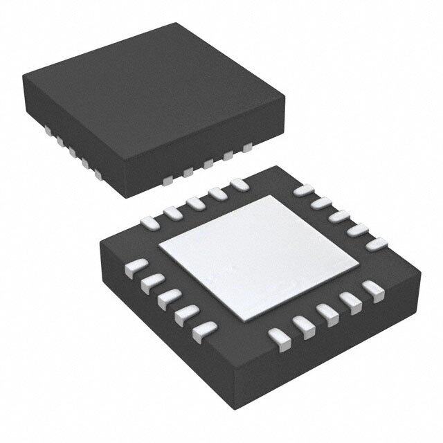
ICGOO电子元器件商城为您提供AD8344ACPZ-REEL7由Analog设计生产,在icgoo商城现货销售,并且可以通过原厂、代理商等渠道进行代购。 AD8344ACPZ-REEL7价格参考¥40.03-¥69.65。AnalogAD8344ACPZ-REEL7封装/规格:RF 混频器, RF Mixer IC Cellular, ISM Down Converter 400MHz ~ 1.2GHz 16-LFCSP (3x3)。您可以下载AD8344ACPZ-REEL7参考资料、Datasheet数据手册功能说明书,资料中有AD8344ACPZ-REEL7 详细功能的应用电路图电压和使用方法及教程。
Analog Devices Inc.的AD8344ACPZ-REEL7是一款高性能、宽频带射频(RF)混频器,广泛应用于通信、测试测量设备和工业控制系统等领域。该器件支持高频率范围,适用于需要高线性度和低噪声的射频信号处理场景。

其主要应用场景包括:

1. 无线通信系统:用于基站、微波通信设备和软件定义无线电(SDR)系统中,实现信号的上变频或下变频处理,支持多频段操作。

2. 测试与测量仪器:应用于频谱分析仪、信号分析仪和网络分析仪等设备中,作为关键的信号转换模块,确保高精度信号处理。

3. 工业与仪表应用:用于工业自动化系统中的射频信号检测和处理,如传感器信号转换、远程监控系统等。

4. 军事与航空航天:在雷达系统、导航设备和通信终端中,提供高稳定性和可靠性的射频混频功能。

AD8344采用紧凑的TSSOP封装,功耗低、集成度高,适合高密度PCB设计,适用于要求高性能和小型化的现代电子系统。
| 参数 | 数值 |
| 产品目录 | |
| 描述 | IC MXR 400MHZ-1.2GHZ DWN 16LFCSP |
| 产品分类 | |
| 品牌 | Analog Devices Inc |
| 数据手册 | |
| 产品图片 |
|
| 产品型号 | AD8344ACPZ-REEL7 |
| PCN其它 | |
| RF类型 | 手机,ISM |
| rohs | 无铅 / 符合限制有害物质指令(RoHS)规范要求 |
| 产品系列 | AD8344 |
| 产品目录页面 | |
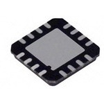
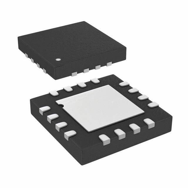
| 供应商器件封装 | 16-LFCSP-VQ (3x3) |
| 其它名称 | AD8344ACPZ-REEL7DKR |
| 包装 | Digi-Reel® |
| 噪声系数 | 10.5dB |
| 增益 | 9.25dB |
| 封装/外壳 | 16-VFQFN 裸露焊盘,CSP |
| 标准包装 | 1 |
| 混频器数 | 1 |
| 电压-电源 | 4.75 V ~ 5.25 V |
| 电流-电源 | 95mA |
| 视频文件 | http://www.digikey.cn/classic/video.aspx?PlayerID=1364138032001&width=640&height=505&videoID=2245193150001 |
| 辅助属性 | 降频变频器 |
| 频率 | 400MHz ~ 1.2GHz |


- 商务部:美国ITC正式对集成电路等产品启动337调查
- 曝三星4nm工艺存在良率问题 高通将骁龙8 Gen1或转产台积电
- 太阳诱电将投资9.5亿元在常州建新厂生产MLCC 预计2023年完工
- 英特尔发布欧洲新工厂建设计划 深化IDM 2.0 战略
- 台积电先进制程称霸业界 有大客户加持明年业绩稳了
- 达到5530亿美元!SIA预计今年全球半导体销售额将创下新高
- 英特尔拟将自动驾驶子公司Mobileye上市 估值或超500亿美元
- 三星加码芯片和SET,合并消费电子和移动部门,撤换高东真等 CEO
- 三星电子宣布重大人事变动 还合并消费电子和移动部门
- 海关总署:前11个月进口集成电路产品价值2.52万亿元 增长14.8%


PDF Datasheet 数据手册内容提取
Active Receive Mixer, 400 MHz to 1.2 GHz Data Sheet AD8344 FEATURES FUNCTIONAL BLOCK DIAGRAM Broadband RF port: 400 MHz to 1.2 GHz PDC WDN XRB OMM Conversion gain: 4.5 dB V P E C 12 11 10 9 Noise figure: 10.5 dB Input IP3: 24 dBm COMM 13 BIAS 8 COMM Input P1dB: 8.5 dBm RFCM 14 7 IFOP LO drive: 0 dBm RFIN 15 6 IFOM External control of mixer bias for low power operation VPMX 16 5 COMM Single-ended, 50 Ω RF and LO input ports 1 2 3 4 ESPxionpwgoelsere--dsduo ppwapndl ydm loeop dLeFerC aStiPo:n 3: 5m Vm a ×t 834 m mmA VPLO LOCM LOIN COMM 04826-0-001 Figure 1. APPLICATIONS Cellular base station receivers ISM receivers Radio links RF Instrumentation GENERAL DESCRIPTION The AD8344 is a high performance, broadband active mixer. It The open-collector differential outputs provide excellent balance is well suited for demanding receive-channel applications that and can be used with a differential filter or IF amplifier, such as require wide bandwidth on all ports and very low intermodulation the AD8369 or AD8351. These outputs may also be converted distortion and noise figure. to a single-ended signal using a matching network or a trans- former (balun). When centered on the VPOS supply voltage, The AD8344 provides a typical conversion gain of 4.5 dB at each of the differential outputs may swing 2.5 V p-p. 890 MHz. The integrated LO driver supports a 50 Ω input impedance with a low LO drive level, helping to minimize The AD8344 is fabricated on an Analog Devices proprietary, external component count. high performance SiGe IC process. The AD8344 is available in a 16-lead LFCSP package. It operates over the −40°C to +85°C The single-ended 50 Ω broadband RF port allows for easy temperature range. An evaluation board is also available. interfacing to both active devices and passive filters. The RF input accepts input signals as large as 1.7 V p-p or 8.5 dBm (re: 50 Ω) at P1dB. Rev. A Document Feedback Information furnished by Analog Devices is believed to be accurate and reliable. However, no responsibility is assumed by Analog Devices for its use, nor for any infringements of patents or other One Technology Way, P.O. Box 9106, Norwood, MA 02062-9106, U.S.A. rights of third parties that may result from its use. Specifications subject to change without notice. No license is granted by implication or otherwise under any patent or patent rights of Analog Devices. Tel: 781.329.4700 ©2004–2018 Analog Devices, Inc. All rights reserved. Trademarks and registered trademarks are the property of their respective owners. Technical Support www.analog.com
AD8344 Data Sheet TABLE OF CONTENTS Features .............................................................................................. 1 Circuit Description......................................................................... 13 Applications ....................................................................................... 1 AC Interfaces ................................................................................... 14 Functional Block Diagram .............................................................. 1 IF Port .......................................................................................... 14 General Description ......................................................................... 1 LO Considerations ..................................................................... 15 Revision History ............................................................................... 2 Bias Resistor Selection ............................................................... 16 Specifications ..................................................................................... 3 Conversion Gain and IF Loading ............................................. 16 AC Performance ............................................................................... 4 Low IF Frequency Operation.................................................... 17 Absolute Maximum Ratings ............................................................ 5 Evaluation Board ............................................................................ 18 ESD Caution .................................................................................. 5 Outline Dimensions ....................................................................... 20 Pin Configuration and Function Descriptions ............................. 6 Ordering Guide .......................................................................... 20 Typical Performance Characteristics ............................................. 7 REVISION HISTORY 4/2018—Rev. 0 to Rev. A Changes to Figure 2 and Table 4 ..................................................... 6 Updated Outline Dimensions ....................................................... 20 Changes to Ordering Guide .......................................................... 20 6/2004—Revision 0: Initial Version Rev. A | Page 2 of 20
Data Sheet AD8344 SPECIFICATIONS V = 5 V, T = 25°C, f = 890 MHz, f = 1090 MHz, LO power = 0 dBm, Z = 50 Ω, R = 2.43 kΩ, unless otherwise noted. S A RF LO O BIAS Table 1. Parameter Conditions Min Typ Max Unit RF INPUT INTERFACE (Pin 15, RFIN and Pin 14, RFCM) Return Loss 10 dB DC Bias Level Internally generated; port must be ac-coupled 2.6 V OUTPUT INTERFACE Output Impedance Differential impedance, f = 200 MHz 9||1 kΩ||pF DC Bias Voltage Externally generated 4.75 V 5.25 V S Power Range Via a 4:1 balun 13 dBm LO INTERFACE LO Power −10 0 +4 dBm Return Loss 10 dB DC Bias Voltage Internally generated; port must be ac-coupled V − 1.6 V S POWER-DOWN INTERFACE PWDN Threshold V − 1.4 V S PWDN Response Time Device enabled, IF output to 90% of its final level 0.4 µs Device disabled, supply current < 5 mA 0.01 µs PWDN Input Bias Current Device enabled −80 µA Device disabled 100 µA POWER SUPPLY Positive Supply Voltage 4.75 V 5.25 V S Quiescent Current VPDC Supply current for bias cells 5 mA VPMX, IFOP, IFOM Supply current for mixer, R = 2.43 kΩ 44 mA BIAS VPLO Supply current for LO limiting amplifier 35 mA Total Quiescent Current 73 84 95 mA Power-Down Current Device disabled 500 µA Rev. A | Page 3 of 20
AD8344 Data Sheet AC PERFORMANCE V = 5 V, T = 25°C, LO power = 0 dBm, Z = 50 Ω, R = 2.43 kΩ, unless otherwise noted. S A O BIAS Table 2. Parameter Conditions Min Typ Max Unit RF Frequency Range 400 1200 MHz LO Frequency Range High Side LO 470 1600 MHz IF Frequency Range 70 400 MHz Conversion Gain f = 450 MHz, f = 550 MHz, f = 100 MHz 9.25 dB RF LO IF f = 890 MHz, f = 1090 MHz, f = 200 MHz 4.5 dB RF LO IF SSB Noise Figure f = 450 MHz, f = 550 MHz, f = 100 MHz 7.75 dB RF LO IF f = 890 MHz, f = 1090 MHz, f = 200 MHz 10.5 dB RF LO IF Input Third-Order Intercept f = 450 MHz, f = 451 MHz, f = 550 MHz, 14 dBm RF1 RF2 LO f = 100 MHz, each RF tone = −10 dBm IF f = 890 MHz, f = 891 MHz, f = 1090 MHz, 24 dBm RF1 RF2 LO f = 200 MHz, each RF tone = −10 dBm IF Input Second-Order Intercept f = 450 MHz, f = 500 MHz, f = 550 MHz, f = 100 MHz 36 dBm RF1 RF2 LO IF f = 890 MHz, f = 940 MHz, f = 1090 MHz, f = 200 MHz 51 dBm RF1 RF2 LO IF Input 1 dB Compression Point f = 450 MHz, f = 550 MHz, f = 100 MHz 2.5 dBm RF LO IF f = 890 MHz, f = 1090 MHz, f = 200 MHz 8.5 dBm RF LO IF LO to IF Output Feedthrough LO Power = 0 dBm, f = 890 MHz, f = 1090 MHz −23 dBc RF LO LO to RF Input Leakage LO Power = 0 dBm, f = 890 MHz, f = 1090 MHz −48 dBc RF LO RF to IF Output Feedthrough RF Power = −10 dBm, f = 890 MHz, f = 1090 MHz −32 dBc RF LO IF/2 Spurious RF Power = −10 dBm, f = 890 MHz, f = 1090 MHz −66 dBm RF LO Rev. A | Page 4 of 20
Data Sheet AD8344 ABSOLUTE MAXIMUM RATINGS Stresses at or above those listed under Absolute Maximum Table 3. Ratings may cause permanent damage to the product. This is a Parameter Rating stress rating only; functional operation of the product at these Supply Voltage, V 5.5 V S or any other conditions above those indicated in the operational RF Input Level 12 dBm section of this specification is not implied. Operation beyond LO Input Level 12 dBm the maximum operating conditions for extended periods may PWDN Pin V + 0.5 V S affect product reliability. IFOP, IFOM Bias Voltage 5.5 V ESD CAUTION Minimum Resistor from EXRB to COMM 2.4 kΩ Internal Power Dissipation 580 mW θ 77°C/W JA Maximum Junction Temperature 125°C Operating Temperature Range −40°C to +85°C Storage Temperature Range −65°C to +150°C Lead Temperature Range (Soldering 60 sec) 300°C Rev. A | Page 5 of 20
AD8344 Data Sheet PIN CONFIGURATION AND FUNCTION DESCRIPTIONS PMX FIN FCM OMM V R R C 6 5 4 3 1 1 1 1 VPLO1 12VPDC LOCM2 AD8344 11PWDN TOP VIEW LOIN3 (Not to Scale) 10EXRB COMM4 9 COMM 5 6 7 8 M M P M M O O M N1.OEMTXUEPSSOTS BEED C POCOANDN. IFETCHTEIFE EDX COTPOO SAEGDN PDA.D 04826-0-002 Figure 2. 16-Lead LFCSP Table 4. Pin Function Descriptions Pin No. Mnemonic Function 1 VPLO Positive Supply Voltage for the LO Buffer: 4.75 V to 5.25 V. 2 LOCM AC Ground for Limiting LO Amplifier, AC-Coupled to Ground. 3 LOIN LO Input. Nominal input level 0 dBm, input level range −10 dBm to +4 dBm, re: 50 Ω, ac-coupled. 4, 5, 8, 9, 13 COMM Device Common (DC Ground). 6, 7 IFOM, IFOP Differential IF Outputs; Open Collectors, Each Requires DC Bias of 5.00 V (Nominal). 10 EXRB Mixer Bias Voltage, Connect Resistor from EXRB to Ground, Typical Value of 2.43 kΩ Sets Mixer Current to Nominal Value. Minimum resistor value from EXRB to ground = 2.4 kΩ. 11 PWDN Connect to Ground for Normal Operation. Connect pin to V for disable mode. S 12 VPDC Positive Supply Voltage for the DC Bias Cell: 4.75 V to 5.25 V. 14 RFCM AC Ground for RF Input, AC-Coupled to Ground. 15 RFIN RF Input. Must be ac-coupled. 16 VPMX Positive Supply Voltage for the Mixer: 4.75 V to 5.25 V. EPAD Exposed Pad. The exposed pad must be connected to AGND. Rev. A | Page 6 of 20
Data Sheet AD8344 TYPICAL PERFORMANCE CHARACTERISTICS 12 10 IF = 70MHz RF = 450MHz IF = 100MHz 9 10 IF = 200MHz IF = 400MHz 8 8 7 6 B) 6 B) d d N ( N ( 5 GAI 4 GAI 4 RF = 890MHz 2 3 2 –20 04826-0-010 01 04826-0-011 400 500 600 700 800 900 1000 1100 1200 80 120 160 200 240 280 320 360 400 RF FREQUENCY (MHz) IF FREQUENCY (MHz) Figure 3. Conversion Gain vs. RF Frequency Figure 6. Conversion Gain vs. IF Frequency 6.0 45 NORMAL(MEAN = 4.47, 5.5 STD DEV = 0.18) 40 GAIN PERCENTAGE 5.0 4.5 35 4.0 30 E GAIN (dB) 233...505 RCENTAG 2205 E 2.0 P 15 1.5 10 1.0 0.05 04826-0-022 05 04826-0-031 –10 –9 –8 –7 –6 –5 –4 –3 –2 –1 0 1 2 3 4 3.6 3.8 4.0 4.2 4.4 4.6 4.8 5.0 5.2 5.4 LO LEVEL (dBm) GAIN (dB) Figure 4. Conversion Gain vs. LO Power, FRF = 890 MHz, FIF = 200 MHz Figure 7. Conversion Gain Distribution, FRF = 890 MHz, FIF = 200 MHz 7.0 VS = 4.75V 6.5 VS = 5.0V VS = 5.25V 6.0 5.5 5.0 B) d N ( 4.5 AI G 4.0 3.5 3.0 22..50 04826-0-018 –40 –30 –20 –10 0 10 20 30 40 50 60 70 80 TEMPERATURE (°C) Figure 5. Conversion Gain vs. Temperature, FRF = 890 MHz, FLO = 1090 MHz Rev. A | Page 7 of 20
AD8344 Data Sheet 28 30 IF = 70MHz 26 IIFF == 120000MMHHzz 28 IF = 400MHz 26 24 RF = 890MHz 24 22 m) m) B B 22 P3 (d 20 P3 (d 20 T I 18 T I PU PU 18 N N I 16 I 16 RF = 450MHz 14 14 1120 04826-0-012 1102 04826-0-013 400 500 600 700 800 900 1000 1100 1200 80 120 160 200 240 280 320 360 400 RF FREQUENCY (MHz) IF FREQUENCY (MHz) Figure 8. Input IP3 vs. RF Frequency (RF Tone Spacing = 1 MHz) Figure 11. Input IP3 vs. IF Frequency (RF Tone Spacing = 1 MHz) 25.0 35 NORMAL(MEAN = 24.023, 24.5 STD DEV = 0.24) IP3 PERCENTAGE 30 24.0 23.5 25 m) P3 (dB 2223..50 NTAGE 20 INPUT I 22.0 PERCE 15 21.5 10 21.0 2200..05–10 –9 –8 –7 –6 –5 –4 –3 –2 –1 0 1 2 3 404826-0-023 05 04826-0-032 23.0 23.2 23.4 23.6 23.8 24.0 24.2 24.4 24.6 24.8 25.0 LO LEVEL (dBm) INPUT IP3 (dBm) Figure 9. Input IP3 vs. LO Power, Figure 12. Input IP3 Distribution, FRF1 = 890 MHz, FRF2 = 891 MHz, FLO = 1090 MHz FRF1 = 890 MHz, FRF2 = 891 MHz, FLO = 1090 MHz 30 VS = 4.75V 29 VS = 5.0V VS = 5.25V 28 27 m) B 26 d P3 ( 25 T I PU 24 N I 23 22 2210 04826-0-019 –40 –30 –20 –10 0 10 20 30 40 50 60 70 80 TEMPERATURE (°C) Figure 10. Input IP3 vs. Temperature, FRF1 = 890 MHz, FRF2 = 891 MHz, FLO = 1090 MHz Rev. A | Page 8 of 20
Data Sheet AD8344 50 60 58 48 56 RF = 890MHz 46 54 52 44 m) m) 50 B 42 B 48 P2 (d 40 P2 (d 46 PUT I 38 PUT I 4424 RF = 450MHz IN 36 IN 40 38 34 IF = 70 36 3320 IIIFFF === 214000000 04826-0-033 333024 04826-0-015 400 500 600 700 800 900 1000 1100 1200 80 120 160 200 240 280 320 360 400 RF FREQUENCY (MHz) IF FREQUENCY (MHz) Figure 13. Input IP2 vs. RF Frequency (RF Tone Spacing = 50 MHz) Figure 16. Input IP2 vs. IF Frequency (RF Tone Spacing = 50 MHz) 60 35 58 NORMAL(MEAN = 48.96, STD DEV = 01.17) 56 30 IIP2 PERCENTAGE 54 52 25 m) 50 P2 (dB 4468 NTAGE 20 PUT I 4424 ERCE 15 IN 40 P 38 10 36 333024 04826-0-034 05 04826-0-035 –10 –9 –8 –7 –6 –5 –4 –3 –2 –1 0 1 2 3 4 44 45 46 47 48 49 50 51 52 53 54 55 LO LEVEL (dBm) INPUT IP2 (dBm) Figure 14. Input IP2 vs. LO Power, Figure 17. Input IP2 Distribution, FRF = 890 MHz, FRF = 890 MHz, FLO = 1090 MHz (RF Tone Spacing = 50 MHz) FLO = 1090 MHz (RF Tone Spacing = 50 MHz) 54 4.75V 5.0V 5.25V 52 m) 50 B d 2 ( 48 P T I U 46 P N I 44 4402 04826-0-037 –40 –30 –20 –10 0 10 20 30 40 50 60 70 80 TEMPERATURE (C) Figure 15. Input IP2 vs. Temperature, FRF = 890 MHz, FLO = 1090 MHz (RF Tone Spacing = 50 MHz) Rev. A | Page 9 of 20
AD8344 Data Sheet 12 10 IF = 70MHz IF = 100MHz 9 10 IIFF == 240000MMHHzz 8 RF = 890MHz 7 m) 8 m) dB dB 6 B ( B ( d 6 d 5 1 1 P P UT UT 4 P P N 4 N I I 3 RF = 450MHz 2 2 0 04826-0-016 10 04826-0-017 400 500 600 700 800 900 1000 1100 1200 80 120 160 200 240 280 320 360 400 RF FREQUENCY (MHz) IF FREQUENCY (MHz) Figure 18. Input P1dB vs. RF Frequency Figure 21. Input P1dB vs. IF Frequency 9.0 60 NORMAL(MEAN = 8.50, 8.8 55 STD DEV = 0.38) INPUT P1dB PERCENTAGE 8.6 50 45 8.4 m) 40 B (dB 8.2 AGE 35 d 8.0 T P1 EN 30 UT 7.8 RC 25 P E N P I 7.6 20 15 7.4 77..02–10 –9 –8 –7 –6 –5 –4 –3 –2 –1 0 1 2 3 404826-0-024 1050 04826-0-036 7.0 7.5 8.0 8.5 9.0 9.5 10.0 LO LEVEL (dBm) INPUT P1dB (dBm) Figure 19. Input P1dB vs. LO Power, FRF = 890 MHz, FLO = 1090 MHz Figure 22. Input P1dB Distribution, FRF = 890 MHz, FLO = 1090 MHz 10.0 VS = 4.75V 9.5 VS = 5.0V VS = 5.25V 9.0 8.5 m) dB 8.0 B ( d 7.5 1 P UT 7.0 P N I 6.5 6.0 55..50 04826-0-020 –40 –30 –20 –10 0 10 20 30 40 50 60 70 80 TEMPERATURE (°C) Figure 20. Input P1dB vs. Temperature, FRF = 890 MHz, FLO = 1090 MHz Rev. A | Page 10 of 20
Data Sheet AD8344 25 100 14 INPUT IP3 95 12 20 90 10 85 A) 3 (dBm) 15 CURRENT 80 RENT (m B (dBm) 8 P 75 R d 6 NF AND I 10 NOISE FIGURE 7605 SUPPLY CU INPUT P1 24 5 60 0 5550 04826-0-026 –20 04826-0-025 2.4 2.6 2.8 3.0 3.2 3.4 3.6 3.8 4.0 2.4 2.6 2.8 3.0 3.2 3.4 3.6 3.8 4.0 RBIAS (kΩ) RBIAS (kΩ) Figure 23. Noise Figure, Input IP3 and Supply Current vs. RBIAS, FRF1 = 890 MHz, Figure 26. Input P1dB vs. RBIAS, FRF = 890 MHz, FLO = 1090 MHz FRF2 = 891 MHz, FLO = 1090 MHz 14 11.0 10.5 13 890MHz 10.0 m) 12 m) B B 9.5 d d B ( 11 B ( 9.0 S S S S RE 10 RE 8.5 U U G G FI 9 FI 8.0 E E OIS OIS 7.5 N 8 N 450MHz IF = 70 7.0 76 IIIFFF === 124000000 04826-0-027 66..50 04826-0-028 400 500 600 700 800 900 1000 1100 1200 70 100 150 200 250 300 350 400 RF FREQUENCY (MHz) IF FREQUENCY (MHz) Figure 24. Noise Figure vs. RF Frequency Figure 27. Noise Figure vs. IF Frequency 13.5 100 VS = 4.75V 13.0 95 VVSS == 55..02V5V m) 12.5 90 B d B ( A) 85 FIGURE SS 1121..05 URRENT (m 8705 E C S OI 11.0 N 70 1100..50 04826-0-029 6650 04826-0-021 –15 –13 –11 –9 –7 –5 –3 –1 1 3 5 –40 –30 –20 –10 0 10 20 30 40 50 60 70 80 LO POWER (dBm) TEMPERATURE (°C) Figure 25. Noise Figure vs. LO Power, FRF = 890 MHz, FLO = 1090 MHz Figure 28. Total Supply Current vs. Temperature Rev. A | Page 11 of 20
AD8344 Data Sheet 90 90 120 60 120 60 150 30 150 30 1.6GHz 400MHz 180 0 180 0 400MHz 210 1.2GHz 330 210 330 240 300 240 300 270 04826-0-051 270 04826-0-052 Figure 29. RFIN Return Loss vs. RF Frequency Figure 32. LOIN Return Loss vs. LO Frequency 0 0 –5 –5 –10 –10 Bc)–15 Bc) d d–15 H ( H ( G–20 G OU OU–20 R–25 R H H DT DT–25 E–30 E E E F F –30 –35 ––4450 04826-0-053 ––4305 04826-0-054 400 500 600 700 800 900 1000 1100 1200 400 600 800 1000 1200 1400 1600 RF FREQUENCY (MHz) LO FREQUENCY (MHz) Figure 30. RF to IF Feedthrough vs. RF Frequency, Figure 33. LO to IF Feedthrough vs. LO Frequency, LO Power = 0 dBm FLO = 1090 MHz, RF Power = −10 dBm 0 14000 3.0 –10 12000 2.5 –20 GE (dBc)––4300 ΩANCE ()108000000 21..05 ANCE (pF) KA ST CIT EA–50 ESI PA L R 6000 1.0 A C –60 4000 0.5 ––8700 04826-0-055 2000 0 04826-0-030 400 600 800 1000 1200 1400 1600 70 120 170 220 270 320 370 LO FREQUENCY (MHz) FREQUENCY (MHz) Figure 31. LO to RF Leakage vs. LO Frequency, LO Power = 0 dBm Figure 34. IF Port Output Resistance and Capacitance vs. IF Frequency Rev. A | Page 12 of 20
Data Sheet AD8344 CIRCUIT DESCRIPTION The AD8344 is a down converting mixer optimized for operation EXTERNAL BIAS within the input frequency range of 400 MHz to 1.2 GHz. It has VPDC RESISTOR PWDN a single-ended, 50 Ω RF input, as well as a single-ended, 50 Ω VPMX local oscillator (LO) input. The IF outputs are differential open BIAS collectors. The mixer current can be adjusted by the value of an RFIN SE IFOP external resistor to optimize performance for gain compression TO RFCM DIFF IFOM and intermodulation or for low power operation. Figure 35 shows the basic blocks of the mixer, which includes the LO bcourfefe. r, RF voltage-to-current converter, bias cell, and mixing INLPOUT VPLO 04826-0-003 The RF voltage to RF current conversion is done via an inductively Figure 35. AD8344 Simplified Schematic degenerated differential pair. When one side of the differential As shown in Figure 36, the IF output pins, IFOP and IFOM, are pair is ac grounded, the other input can be driven single-ended. directly connected to the open collectors of the NPN transistors The RF inputs can also be driven differentially. The voltage-to- in the mixer core so the differential and single-ended impedances current converter then drives the emitters of a four-transistor looking into this port are relatively high, on the order of several switching core. This switching core is driven by an amplified kΩ. A connection between the supply voltage and these output version of the local oscillator signal connected to the LO input. pins is required for proper mixer core operation. There are three limiting gain stages between the external LO signal IFOP IFOM and the switching core. The first stage converts the single-ended LO drive to a well balanced differential drive. The differential drive then passes through two more gain stages, which ensures a limited signal drives the switching core. This affords the user a lower LO drive requirement, while maintaining excellent distortion LOIN and compression performance. The output signal of these three LO RFIN RFCM gain stages drives the four transistors within the mixer core to commutate at the rate of the local oscillator frequency. The output of the mixer core is taken directly from these open collectors. The open collector outputs present a high impedance at the IF freq- uimenpceyd. aTnhcee pcorensveenrtseido nto g tahiens eo of ptheen mcoilxleecrt odresp. eInn dcsh adriarcetcetrliyz aotnio tnh,e COMM 04826-0-003 a 200 Ω load was presented to the device via a 4:1 impedance Figure 36. Mixer Core Simplified Schematic transformer. The AD8344 has three pins for the supply voltage: VPDC, The AD8344 also features a power-down function. Application VPMX, and VPLO. These pins are separated to minimize or of a logic low at the PWDN pin allows normal operation. A high eliminate possible parasitic coupling paths within the AD8344 logic level at the PWDN pin shuts down the AD8344. Power that can cause spurious signals or reduced interport isolation. consumption when the device is disabled is less than 10 mW. Consequently, each of these pins are well bypassed and decoupled The bias for the mixer is set with an external resistor from the as close to the AD8344 as possible. EXRB pin to ground. The value of this resistor directly affects the dynamic range of the mixer. The external resistor must not be lower than 2.4 kΩ. Permanent damage to the device occurs if values below 2.4 kΩ are used. Rev. A | Page 13 of 20
AD8344 Data Sheet AC INTERFACES The AD8344 is a high-side downconverter. It is designed to down- 90 convert radio frequencies (RF) to lower intermediate frequencies 120 60 (IF) using a high-side local oscillator (LO). The LO is injected into the mixer core at a frequency greater than the desired input RF frequency. The difference between the LO and RF frequencies, f − f is the IF frequency, f . In addition to the desired RF signal, 150 30 LO RF, IF an RF image is downconverted to the same IF frequency. The image frequency is at f + f . The conversion gain of the AD8344 LO IF 10MHz decreases with increasing input frequency. By choosing to use a 180 0 high-side LO the image frequency at f + f is translated with LO IF less conversion gain than the desired RF signal at f − f . Addi- LO IF tionally, any wideband noise present at the image frequency is 210 330 downconverted with less conversion gain than if a low-side LO 500MHz was applied. In general, use a high-side LO with the AD8344 to ensure optimal noise performance and image rejection. 240 300 T40h0e MADH8z3 t4o4 1 i2s0 d0e MsigHnze dfr teoq uopenercayt er aunsgine,g w RiFth f rheiqguhe-snicdiee sL iOn the 270 04826-0-040 Figure 37. IF Port Reflection Coefficient from 10 MHz to 500 MHz injection within the 470 MHz to 1600 MHz range. It is essential to ac-couple RF and LO ports to prevent dc offsets from skewing IF PORT the mixer core in an asymmetrical manner, potentially degrading The IF port uses an open collector differential output interface. linear input swing and impacting distortion and input compression The NPN open collectors can be modeled as high impedance characteristics. current sources. The stray capacitance associated with the IC The AD8344 RFIN port presents a 50 Ω impedance relative to package presents a slightly capacitive source impedance as in RFCM. In order to ensure a good impedance match, the RFIN Figure 37. In general, the IFOP and IFOM output ports can be ac-coupling capacitor must be large enough in value so that the modeled as current sources with an impedance of ~10 kΩ in presented reactance is negligible at the intended RF frequency. parallel with ~1 pF of shunt capacitance. Circuit board traces Additionally, the RFCM bypassing capacitor must be sufficiently connecting the IF outputs to the load must be narrow and short large to provide a low impedance return path to board ground. to prevent excessive capacitive loading. In order to maintain the Low inductance ceramic grade capacitors of no more than specified conversion gain of the mixer, the IF output ports must 330 pF are sufficient for most applications. be loaded into 200 Ω. It is not necessary to attempt to provide a conjugate match to the IF port output source impedance. If the Similarly the LOIN port provides a 50 Ω load impedance with IF signal needs to be delivered to a remote load, more than a common-mode decoupling on LOCM. Again, common grade few centimeters away, it can be necessary to use an appropriate ceramic capacitors provide sufficient signal coupling and buffer amplifier to present a real 200 Ω loading impedance at bypassing of the LO interface. the IF output interface. The buffer amplifier must have the appropriate source impedance to match the characteristic impedance of the selected transmission line. An example is provided in Figure 38, where the AD8351 differential amplifier is used to drive a pair of 75 Ω transmission lines. The gain of the buffer can be independently set by choosing an appropriate gain resistor, R . G +VS AD8344 +VS COMM 8 RFC IFOP 7 + Tx LINE ZO = 75Ω 200Ω RG AD8351 ZL IFOM 6 – Tx LINE ZO = 75Ω COMM 5 RFC +VS ZL = 200Ω 04826-0-041 Figure 38. AD8351 Used as Transmission Line Driver and Impedance Buffer Rev. A | Page 14 of 20
Data Sheet AD8344 The high input impedance of the AD8351 allows a shunt differ- 90 ential termination to provide the desired 200 Ω load to the 120 60 AD8344 IF output port. It is necessary to bias the open collector outputs using one of the schemes presented in Figure 39 and Figure 40. Figure 39 150 30 illustrates the application of a center-tapped impedance trans- 50MHz former. The turns ratio of the transformer must be selected to REAL CHOKES provide the desired impedance transformation. In the case of a 180 0 50 Ω load impedance, use a 4-to-1 impedance ratio transformer 50MHz to transform the 50 Ω load into a 200 Ω differential load at the 500MHz IDEAL CHOKES IF output pins. Figure 40 illustrates a differential IF interface 210 330 where pull-up choke inductors are used to bias the open-collector 500MHz outputs. The shunting impedance of the choke inductors used to couple dc current into the mixer core must be large enough at the IF frequency of operation as to not load down the output 240 300 ccuurrrreenntt bheafnodrlei nrega ccahpianbgi ltihtye oinf ttehned seedle lcotaedd .c Ahodkdei tiinodnuaclltyo,r tsh me udsct 270 04826-0-044 Figure 41. IF Port Loading Effects due to Finite-Q Pull-Up Inductors be at least 45 mA. The self resonant frequency of the selected (Murata BLM18HD601SN1D Chokes) choke must be higher than the intended IF frequency. A variety LO CONSIDERATIONS of suitable choke inductors are commercially available from manufacturers such as Murata and Coilcraft. An impedance The LO signal must have adequate phase noise characteristics and transforming network can be required to transform the final reasonable low second harmonic content to prevent degradation of load impedance to 200 Ω at the IF outputs. There are several the noise figure performance of the AD8344. A LO plagued with reference books that explain general impedance matching poor phase noise can result in reciprocal mixing, a mechanism procedures, including: that causes spectral spreading of the downconverted signal, • Chris Bowick, RF Circuit Design, Newnes, Reprint Edition, limiting the sensitivity of the mixer at frequencies close-in to any large input signals. The internal LO buffer provides enough gain 1997. to hard limit the input LO and provide fast switching of the mixer • David M. Pozar, Microwave Engineering, Wiley Text Books, core. Odd harmonic content present on the LO drive signal should Second Edition, 1997. not impact mixer performance; however, even-order harmonics • Guillermo Gonzalez, Microwave Transistor Amplifiers: cause the mixer core to commutate in an unbalanced manner, Analysis and Design, Prentice Hall, Second Edition, 1996. potentially degrading noise performance. Simple, lumped element, +VS low-pass filtering can be applied to help reject the harmonic AD8344 content of a given local oscillator, as illustrated in Figure 42. The COMM 8 filter depicted is a common 3-pole Chebyshev, designed to main- 4:1 IF OUT IFOP 7 ZO = 50Ω tain a 1-to-1 source-to-load impedance ratio with no more than 0.5 dB of ripple in the pass band. Other filter structures can be IFOM 6 COMM 5 ZL = 200Ω 04826-0-042 enfefgelcitgiivbel ea sl elvoenlgs, aes. gt.h, e~ s3e0c donBd b helaorwm tohnei cf uonf dthame LeOnt aisl. fTilhteer ed to measured frequency response of the Chebyshev filter for a Figure 39. Biasing the IF Port Open Collector Outputs Using a Center-Tapped Impedance Transformer 1200 MHz −3 dB cutoff frequency is presented in Figure 43. +VS AD8344 AD8344 LOCMLOINCOMM COMM 8 RFC RS 2 3 4 IF OUT+ IFOP 7 IMPEDANCE LO L2 ZL = 200Ω TRANSFORMING ZL SOURCE IFOM 6 NETWORK C1 C3 RL IF OUT– COMM 5 RFC FOR RS= RL Figure 40. B+iVaSsing the IF Port Open Collector Outputs 04826-0-043 CfC1 -= F2IL1π.Tf8cE6RR4L CULT2O F=F1 F2.2Rπ8fERcQLUENCC3 Y=21π.f8c3R4L 04826-0-045 Using Pull-Up Choke Inductors Figure 42. Using a Low-Pass Filter to Reduce LO Second Harmonic Rev. A | Page 15 of 20
AD8344 Data Sheet 0 125 85 –5 –10 124 81 –15 A) m ESPONSE (dB)–––322050 IDEAL LPF SFDR (dBc)112223 +VS 7773 LY CURRENT ( R REAL LPF P –35 RBIAS UP 6.8nH S –40 121 69 12 11 10 9 ––5405 4.7pF 4.7pF 04826-0-046 120 VPDC PWADDN83E4XR4B COMM 65 04826-0-047 0.1 1 10 2.4 2.6 2.8 3.0 3.2 3.4 3.6 3.8 4.0 FREQUENCY (GHz) RBIAS (kΩ) Figure 43. Measured and Ideal LO Filter Frequency Response Figure 44. Impact of RBIAS Resistor Selection vs. Spurious-Free Dynamic Range and Power Consumption, BIAS RESISTOR SELECTION FRF = 890 MHz and FLO = 1090 MHz An external bias resistor is used to set the dc current in the CONVERSION GAIN AND IF LOADING mixer core. This provides the ability to reduce power consumption The AD8344 is optimized for driving a 200 Ω differential load. at the expense of decreased dynamic range. Figure 44 shows the Although the device is capable of driving a wide variety of loads, in spurious-free dynamic range (SFDR) of the mixer for a 1 Hz order to maintain optimum distortion and noise performance, noise bandwidth versus the R resistor value. SFDR was BIAS it is advised that the presented load at the IF outputs is reasonably calculated using NF and IIP3 data collected at 900 MHz. close to 200 Ω. Figure 45 illustrates the effect of IF loading on By definition, conversion gain. The mixer outputs behave like Norton equivalent SFDR=2(IIP3−NF−kT−10log(B)) sources, where the conversion gain is the effective transcon- 3 ductance of the mixer multiplied by the loading impedance. where IIP3 is the input third-order intercept in dBm. NF is the The linear differential voltage conversion gain of the mixer can noise figure in dB. kT is the thermal noise power density and is be modeled as −173.86 dBm/Hz at 298°K. B is the noise bandwidth in Hz. g In order to calculate the anticipated SFDR for a given appli- Av=−0.46×RLOAD×1+j×g ×m37.70×f m RF cation, it is necessary to factor in the actual noise bandwidth. For instance, if the IF noise bandwidth is 5 MHz, the anticipated SFDR where RLOAD is the differential loading impedance. gm is the using a 2.43 kΩ RBIAS is 6.66 log10 (5 MHz) less than the 1 Hz mixer transconductance and is equal to 4070/RBIAS. fRF is the data in Figure 44 or ~80 dBc. Using a 2.43 kΩ bias resistor sets frequency of the signal applied to the RF port in GHz. the quiescent power dissipation to ~415 mW for a 5 V supply. If Large impedance loads cause the conversion gain to increase, the RBIAS resistor value is raised to 3.9 kΩ, the SFDR for the same resulting in a decrease in input linearity and allowable signal 5 MHz bandwidth is reduced to ~77.5 dBc and the power dissi- swing. In order to maintain positive conversion gain and preserve pation is reduced to ~335 mW. In low power portable applications, spurious-free dynamic range performance, the differential load it can be advantageous to reduce power consumption by using a presented at the IF port must remain within a range of ~100 Ω larger value of RBIAS, assuming reduced dynamic range perfor- to 250 Ω. mance is acceptable. Rev. A | Page 16 of 20
Data Sheet AD8344 25 15 15 20 B) 12 12 N (d B) Bm) ONVERSION GAI 1105 MODELED MEASURED ERSION GAIN (d 69 96 P3 AND P1dB (d 0LOG–C 5 CONV 3 3 INPUT I 2 0 –5 04826-0-048 0 0 04826-0-049 10 100 1000 10 15 20 25 30 35 40 45 50 IF LOADING (Ω) IF FREQUENCY (MHz) Figure 45. Conversion Gain vs. IF Loading Figure 46. Conversion Gain, Input IP3, and P1dB vs. IF Frequency, FRF = 450 MHz LOW IF FREQUENCY OPERATION 8 28.0 The AD8344 can be used down to arbitrarily low IF frequencies. The conversion gain, noise, and linearity characteristics remain 7 24.5 qanudit eF figlautr aes 4 I7F. fLraerqgueern vcayl uise rpeudlul-cuepd ,i nasd uincdtoicras tmedu isnt bFeig uusreed 4 a6t N (dB) 6 21.0 B (dBm) tchoem lomwoenr- ImFo fdreeq luoeandciniegs .i mA p1e µdHan cche ookf e6 i3n Ωdu actt oarn pIrFe fsreenqtus ean cy ON GAI 5 17.5 ND P1d of 10 MHz, severely loading down the mixer outputs, reducing ERSI P3 A conversion gain, and sacrificing output power. At low IF freq- NV 4 14.0 T I O U uencies, use choke inductors of several hundred µH to bias the C NP I IF outputs. 3 10.5 2 7.0 04826-0-050 10 15 20 25 30 35 40 45 50 IF FREQUENCY (MHz) Figure 47. Conversion Gain, Input IP3, and P1dB vs. IF Frequency, FRF = 890 MHz Rev. A | Page 17 of 20
AD8344 Data Sheet EVALUATION BOARD An evaluation board is available for the AD8344. The evaluation board is configured for single-ended signaling at the IF output port via a balun transformer. The schematic for the evaluation board is presented in Figure 48. Table 5. Evaluation Board Configuration Options Component Function Default Conditions R1, R2, R7, Supply Decoupling. R1, R2, R7 = 0 Ω (Size 0603) C2, C4, C5, C6, Jumpers or power supply decoupling resistors and filter capacitors. C4, C6, C13, C14 = 100 pF C12, C13, C14, (Size 0603) C15 C2, C5, C12, C15 = 0.1 µF (Size 0603) R3, R4 Jumpers in Single-Ended IF Output Circuit. 0 Ω (Size 0603) R6, C11 R resistor that sets the bias current for the mixer core. R6 = 2.43 kΩ (Size 0603) BIAS The capacitor provides ac bypass for R6. C11 = 100 pF (Size 0603) R8 Jumper for pull down of the PWDN pin. R8 = 10 kΩ (Size 0603) R9 Jumper. R9 = 0 Ω (Size 0603) C3 RF Input AC Coupling. Provides dc block for RF input. C3 = 100 pF (Size 0402) C1 RF Common AC Coupling. Provides dc block for RF input common connection. C1 = 100 pF (Size 0402) C8 LO Input AC Coupling. Provides dc block for the LO input. C8 = 100 pF (Size 0402) C7 LO Common AC Coupling. Provides dc block for LO input common connection. C7 = 100 pF (Size 0402) SW1 Power Down. The device is on when the PWDN is connected to ground via SW1. The device is disabled when PWDN is connected to the positive supply (V) via SW1. S T1 IF Output Balun Transformer. Converts differential, high impedance IF output to T1 = TC4-1W, 4:1 (Mini-Circuits) single-ended. When loaded with 50 Ω, this balun presents a 200 Ω load to the mixers collectors. The center tap of the primary is used to supply the bias voltage (V) to the IF output pins. S R11, Z3, Z4 IF Output Interface—IFOP, IFOM. These positions can be used to modify the R11 = 0 Ω (Size 0603) R12, Z1, Z2 impedance presented to the IF outputs. Z3, Z4 = Open R12 = 0 Ω (Size 0603) Z1, Z2 = Open Rev. A | Page 18 of 20
Data Sheet AD8344 POWER DOWN SW1 C11 100pF COMMON R8 0R7 10k R09 2.4R36k VPOS C12 C13 0.1F 100pF C N B M D D R M VP PW EX CO COMM COMM Z1 Z2 OPEN OPEN C1 100pF RFCM IFOP R010 0R3 IF OUTPUT 10C03pF AD8344 R011 TT1C4-1W RF INPUT RFIN IFOM R4 R1 Z3 Z4 0 0 OPEN OPEN VPOS VPMX COMM 0.1CF2 100CpF4 PLO OCM OIN OMM C10104pF V L L C R2 C5 0 C6 100CpF7 C8 C0.115F 0.1F 100pF 100pF LINOPUT VPOS 04826-0-005 Figure 48. Evaluation Board Schematic—Single-Ended IF Output 04826-0-007 04826-0-008 Figure 49. Single-Ended Evaluation Board, Component Side Layout Figure 50. Single-Ended Evaluation Board, Component Side Silkscreen Rev. A | Page 19 of 20
AD8344 Data Sheet OUTLINE DIMENSIONS DETAIL A 3.10 0.30 (JEDEC 95) 3.00 SQ 0.25 PIN 1 2.90 0.20 INDICATOR 0.50 13 16 PI(NSINDE EI1C DAETTAOIRL AAR)EA OPTIONS BSC 12 1 1.65 EXPOSED 1.50 SQ PAD 1.45 9 4 0.50 8 5 0.20 MIN TOP VIEW 0.40 BOTTOM VIEW 0.30 0.80 FOR PROPER CONNECTION OF THE EXPOSED PAD, REFER TO 0.75 SIDE VIEW 0.05 MAX THE PIN CONFIGURATION AND 0.70 FUNCTION DESCRIPTIONS 0.02 NOM SECTION OF THIS DATA SHEET. COPLANARITY SEATING 0.08 PLANE 0.20 REF PKG-004395 COMPLIANTTOJEDEC STANDARDS MO-220-WEED-6. 02-06-2017-A Figure 51. 16-Lead Lead Frame Chip Scale Package [LFCSP] 3 mm × 3 mm Body and 0.75 mm Package Height (CP-16-27) Dimensions in millimeters ORDERING GUIDE Models1, 2 Temperature Range Package Description Package Option Marking Code AD8344ACPZ-REEL7 −40°C to +85°C 16-Lead Lead Frame Chip Scale Package [LFCSP] CP-16-27 JHA AD8344ACPZ-WP −40°C to +85°C 16-Lead Lead Frame Chip Scale Package [LFCSP] CP-16-27 JHA AD8344-EVAL Evaluation Board 1 Z = RoHS Compliant Part. 2 WP = Waffle pack. ©2004–2018 Analog Devices, Inc. All rights reserved. Trademarks and registered trademarks are the property of their respective owners. D04826-0-4/18(A) Rev. A | Page 20 of 20