ICGOO在线商城 > 射频/IF 和 RFID > RF 混频器 > ADL5354ACPZ-R7

 Datasheet下载
- 型号: ADL5354ACPZ-R7
- 制造商: Analog
- 库位|库存: xxxx|xxxx
- 要求:
| 数量阶梯 | 香港交货 | 国内含税 |
| +xxxx | $xxxx | ¥xxxx |
查看当月历史价格
查看今年历史价格
ADL5354ACPZ-R7产品简介:
ICGOO电子元器件商城为您提供ADL5354ACPZ-R7由Analog设计生产,在icgoo商城现货销售,并且可以通过原厂、代理商等渠道进行代购。 ADL5354ACPZ-R7价格参考。AnalogADL5354ACPZ-R7封装/规格:RF 混频器, RF Mixer IC Cellular 2.2GHz ~ 2.7GHz 36-LFCSP-VQ (6x6)。您可以下载ADL5354ACPZ-R7参考资料、Datasheet数据手册功能说明书,资料中有ADL5354ACPZ-R7 详细功能的应用电路图电压和使用方法及教程。
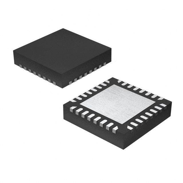
ADL5354ACPZ-R7 是由 Analog Devices Inc.(ADI)生产的一款 RF 混频器,属于 ADL5354 系列。它主要应用于射频和微波通信系统中,支持高频信号的变频处理。以下是其典型应用场景:

1. 无线通信设备
   ADL5354ACPZ-R7 可用于无线基站、中继器和远程无线电单元等设备中。它能够实现频率转换,将射频信号下变频为中频信号,或反之将中频信号上变频为射频信号,满足无线通信系统的收发需求。

2. 测试与测量仪器
   在频谱分析仪、信号发生器和其他射频测试设备中,该混频器可用于信号的频率转换,帮助生成或分析不同频段的信号。

3. 卫星通信系统
   适用于卫星地面站和用户终端中的射频前端模块。它可以处理 L 波段、C 波段或其他频段的信号,支持上下变频操作以适应卫星通信的需求。

4. 雷达系统
   在脉冲雷达或连续波雷达中,ADL5354ACPZ-R7 可用于信号的频率转换,提供高线性度和低失真的性能,确保雷达系统的准确性和可靠性。

5. 点对点无线电链路
   用于微波回传网络中的射频模块,完成信号的上下变频,支持宽带数据传输。

6. 物联网 (IoT) 和工业通信
   在需要高频信号处理的 IoT 设备或工业无线通信系统中,该混频器可以实现高效的频率转换,支持多种协议和标准。

ADL5354ACPZ-R7 的特点是工作频率范围宽(0.05 GHz 至 4 GHz)、高动态范围、低噪声以及易于集成到射频电路中,因此非常适合上述场景中的高性能应用需求。
| 参数 | 数值 |
| 产品目录 | |
| 描述 | IC MIXER 2.2-2.7GHZ 36LFCSP射频混合器 2.5 GHz SINGLE MIXER |
| 产品分类 | |
| 品牌 | Analog Devices Inc |
| 产品手册 | |
| 产品图片 |
|
| rohs | 符合RoHS无铅 / 符合限制有害物质指令(RoHS)规范要求 |
| 产品系列 | RF集成电路,射频混合器,Analog Devices ADL5354ACPZ-R7- |
| 数据手册 | |
| 产品型号 | ADL5354ACPZ-R7 |
| PCN其它 | |
| PCN组件/产地 | |
| RF类型 | 手机 |
| 产品种类 | 射频混合器 |
| 供应商器件封装 | 36-LFCSP(6x6) |
| 其它名称 | ADL5354ACPZ-R7TR |
| 功率增益类型 | 8.6 dB |
| 包装 | 带卷 (TR) |
| 商标 | Analog Devices |
| 噪声系数 | 9.9dB |
| 增益 | 14dB |
| 安装风格 | SMD/SMT |
| 封装 | Reel |
| 封装/外壳 | 36-VFQFN 裸露焊盘,CSP |
| 封装/箱体 | LFCSP-36 |
| 工作电源电压 | 3.3 V to 5 V |
| 工厂包装数量 | 750 |
| 最大功率耗散 | 2.2 W |
| 最大工作温度 | + 85 C |
| 最小工作温度 | - 40 C |
| 标准包装 | 750 |
| 混频器数 | 2 |
| 电压-电源 | 3.3 V ~ 5 V |
| 电流-电源 | 350mA |
| 电源电流 | 350 mA |
| 类型 | Mixer |
| 系列 | ADL5354 |
| 视频文件 | http://www.digikey.cn/classic/video.aspx?PlayerID=1364138032001&width=640&height=505&videoID=2245193150001 |
| 转换损失——最大 | 20 dB |
| 辅助属性 | - |
| 频率 | 2.2GHz ~ 2.7GHz |
| 频率范围 | 2200 MHz to 2700 MHz |


- 商务部:美国ITC正式对集成电路等产品启动337调查
- 曝三星4nm工艺存在良率问题 高通将骁龙8 Gen1或转产台积电
- 太阳诱电将投资9.5亿元在常州建新厂生产MLCC 预计2023年完工
- 英特尔发布欧洲新工厂建设计划 深化IDM 2.0 战略
- 台积电先进制程称霸业界 有大客户加持明年业绩稳了
- 达到5530亿美元!SIA预计今年全球半导体销售额将创下新高
- 英特尔拟将自动驾驶子公司Mobileye上市 估值或超500亿美元
- 三星加码芯片和SET,合并消费电子和移动部门,撤换高东真等 CEO
- 三星电子宣布重大人事变动 还合并消费电子和移动部门
- 海关总署:前11个月进口集成电路产品价值2.52万亿元 增长14.8%


PDF Datasheet 数据手册内容提取
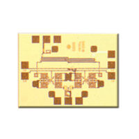
2200 MHz to 2700 MHz, Dual-Balanced Mixer, LO Buffer, IF Amplifier, and RF Balun ADL5354 FEATURES FUNCTIONAL BLOCK DIAGRAM RF frequency range of 2200 MHz to 2700 MHz OS GM MM ON OP LE OS LG P N O N N N P N C IF frequency range of 30 MHz to 450 MHz V M C M M M V M N Power conversion gain: 8.6 dB 36 35 34 33 32 31 30 29 28 SSB noise figure of 10.6 dB MNIN 1 27 LOI2 Input IP3 of 26.1 dBm MNCT 2 26 VGS2 Input P1dB of 10.6 dBm Typical LO power of 0 dBm COMM 3 25 VGS1 Single-ended, 50 Ω RF and LO input ports High isolation SPDT LO input switch VPOS 4 24 VGS0 Single-supply operation: 3.3 V to 5 V COMM 5 23 LOSW Exposed paddle, 6 mm × 6 mm, 36-lead LFCSP 1500 V HBM/500 V FICDM ESD performance VPOS 6 22 PWDN APPLICATIONS COMM 7 21 VPOS Cellular base station receivers ADL5354 DVCT 8 20 COMM Transmit observation receivers Radio link downconverters DVIN 9 19 LOI1 10 11 12 13 14 15 16 17 18 VPOS DVGM COMM DVOP DVON DVLE VPOS DVLG NC 09118-001 Figure 1. GENERAL DESCRIPTION commensurate with the desired level of performance. For low voltage applications, the ADL5354 is capable of operation at The ADL5354 uses a highly linear, doubly balanced, passive mixer voltages as low as 3.3 V with substantially reduced current. For core along with integrated RF and local oscillator (LO) balancing low voltage operation, an additional logic pin is provided to circuitry to allow single-ended operation. The ADL5354 incor- power down (~300 μA) the circuit when desired. porates the RF baluns, allowing for optimal performance over a 2200 MHz to 2700 MHz RF input frequency range. The balanced The ADL5354 is fabricated using a BiCMOS high performance passive mixer arrangement provides good LO-to-RF leakage, IC process. The device is available in a 6 mm × 6 mm, 36-lead typically better than −37 dBm, and excellent intermodulation LFCSP and operates over a −40°C to +85°C temperature range. performance. The balanced mixer core also provides extremely An evaluation board is also available. high input linearity, allowing the device to be used in demanding Table 1. Passive Mixers cellular applications where in-band blocking signals may other- RF Frequency Single Single Mixer Dual Mixer wise result in the degradation of dynamic performance. A high (MHz) Mixer and IF Amp and IF Amp linearity IF buffer amplifier follows the passive mixer core to yield 500 to 1700 ADL5367 ADL5357 ADL5358 a typical power conversion gain of 8 dB and can be used with a 1200 to 2500 ADL5365 ADL5355 ADL5356 wide range of output impedances. 2200 to 2700 ADL5353 ADL5354 The ADL5354 provides two switched LO paths that can be used in time division duplex (TDD) applications where it is desirable to ping-pong between two local oscillators. LO current can be externally set using a resistor to minimize dc current Rev. 0 Information furnished by Analog Devices is believed to be accurate and reliable. However, no responsibility is assumed by Analog Devices for its use, nor for any infringements of patents or other One Technology Way, P.O. Box 9106, Norwood, MA 02062-9106, U.S.A. rights of third parties that may result from its use. Specifications subject to change without notice. No license is granted by implication or otherwise under any patent or patent rights of Analog Devices. Tel: 781.329.4700 www.analog.com Trademarks and registered trademarks are the property of their respective owners. Fax: 781.461.3113 ©2011 Analog Devices, Inc. All rights reserved.
ADL5354 TABLE OF CONTENTS Features..............................................................................................1 Spur Tables......................................................................................15 Applications.......................................................................................1 5 V Performance.........................................................................15 Functional Block Diagram..............................................................1 3.3 V Performance......................................................................15 General Description.........................................................................1 Circuit Description.........................................................................16 Revision History...............................................................................2 RF Subsystem..............................................................................16 Specifications.....................................................................................3 LO Subsystem.............................................................................16 5 V Performance...........................................................................4 Applications Information..............................................................18 3.3 V Performance........................................................................4 Basic Connections......................................................................18 Absolute Maximum Ratings............................................................5 IF Port..........................................................................................18 ESD Caution..................................................................................5 Bias Resistor Selection...............................................................18 Pin Configuration and Function Descriptions.............................6 Mixer VGS Control DAC..........................................................18 Typical Performance Characteristics.............................................7 Evaluation Board............................................................................20 5 V Performance...........................................................................7 Outline Dimensions.......................................................................22 3.3 V Performance......................................................................14 Ordering Guide..........................................................................22 REVISION HISTORY 2/11—Revision 0: Initial Version Rev. 0 | Page 2 of 24
ADL5354 SPECIFICATIONS V = 5 V, I = 350 mA, T = 25°C, f = 2535 MHz, f = 2332 MHz, LO power = 0 dBm, RF power = −10 dBm, R1 = R4 = 1.3 kΩ, R2 = S S A RF LO R5 = 1 kΩ, Z = 50 Ω, VGS0 = VGS1 = VGS2 = 0 V, unless otherwise noted. O Table 2. Parameter Test Conditions/Comments Min Typ Max Unit RF INPUT INTERFACE Return Loss Tunable to >20 dB over a limited bandwidth 20 dB Input Impedance 50 Ω RF Frequency Range 2200 2700 MHz OUTPUT INTERFACE Output Impedance Differential impedance, f = 200 MHz 230||0.75 Ω||pF IF Frequency Range 30 450 MHz DC Bias Voltage1 Externally generated 3.3 5.0 5.5 V LO INTERFACE LO Power −6 0 +10 dBm Return Loss 13 dB Input Impedance 50 Ω LO Frequency Range 1750 2670 MHz POWER-DOWN (PWDN) INTERFACE2 PWDN Threshold 1.0 V Logic 0 Level 0.4 V Logic 1 Level 1.4 V PWDN Response Time Device enabled, IF output to 90% of its final level 160 ns Device disabled, supply current < 5 mA 230 ns PWDN Input Bias Current Device enabled 0 μA Device disabled 70 μA 1 Apply supply voltage from external circuit through choke inductors. 2 PWDN function is intended for use with VS ≤ 3.6 V only. Rev. 0 | Page 3 of 24
ADL5354 5 V PERFORMANCE V = 5 V, I = 350 mA, T = 25°C, f = 2535 MHz, f = 2332 MHz, LO power = 0 dBm, RF power = −10 dBm, R1 = R4 = 1.3 kΩ, R2 = R5 = 1 kΩ, S S A RF LO VGS0 = VGS1 = VGS2 = 0 V, and Z = 50 Ω, unless otherwise noted. O Table 3. Parameter Test Conditions/Comments Min Typ Max Unit DYNAMIC PERFORMANCE Power Conversion Gain Including 4:1 IF port transformer and PCB loss 8.6 dB Voltage Conversion Gain Z = 50 Ω, differential Z = 200 Ω differential 14.6 dB SOURCE LOAD SSB Noise Figure 10.6 dB Input Third-Order Intercept (IIP3) f = 2534.5 MHz, f = 2535.5 MHz, f = 2332 MHz, 26.1 dBm RF1 RF2 LO each RF tone at −10 dBm Input Second-Order Intercept (IIP2) f = 2535 MHz, f = 2585 MHz, f = 2332 MHz, 50 dBm RF1 RF2 LO each RF tone at −10 dBm Input 1 dB Compression Point (IP1dB) 10.6 dBm LO-to-IF Leakage Unfiltered IF output −20.7 dBm LO-to-RF Leakage −37 dBm RF-to-IF Isolation −34 dBc IF/2 Spurious −10 dBm input power −73 dBc IF/3 Spurious −10 dBm input power −71 dBc IF Channel-to-Channel Isolation 52 dB POWER SUPPLY Positive Supply Voltage 4.75 5 5.25 V Quiescent Current LO supply 170 mA IF supply 180 mA Total Quiescent Current V = 5 V 350 mA S 3.3 V PERFORMANCE V = 3.3 V, I = 200 mA, T = 25°C, f = 2535 MHz, f = 2332 MHz, LO power = 0 dBm, R9 = 226 Ω, R14 = 604 Ω, VGS0 = VGS1 = 0 V, S S A RF LO and Z = 50 Ω, unless otherwise noted. O Table 4. Parameter Test Conditions/Comments Min Typ Max Unit DYNAMIC PERFORMANCE Power Conversion Gain Including 4:1 IF port transformer and PCB loss 8 dB Voltage Conversion Gain Z = 50 Ω, differential Z = 200 Ω differential 14 dB SOURCE LOAD SSB Noise Figure 9.9 dB Input Third-Order Intercept (IIP3) f = 2534.5 MHz, f = 2535.5 MHz, f = 2332 MHz, each 17.5 dBm RF1 RF2 LO RF tone at −10 dBm Input Second-Order Intercept (IIP2) f = 2535 MHz, f = 2585 MHz, f = 2332 MHz, each RF 49 dBm RF1 RF2 LO tone at −10 dBm Input 1 dB Compression Point (IP1dB) 7 dBm POWER INTERFACE Supply Voltage 3.0 3.3 3.6 V Quiescent Current Resistor programmable 200 mA Power-Down Current Device disabled 300 μA Rev. 0 | Page 4 of 24
ADL5354 ABSOLUTE MAXIMUM RATINGS Table 5. Parameter Rating Stresses above those listed under Absolute Maximum Ratings Supply Voltage, V 5.5 V may cause permanent damage to the device. This is a stress S RF Input Level 20 dBm rating only; functional operation of the device at these or any LO Input Level 13 dBm other conditions above those indicated in the operational MNOP, MNON, DVOP, DVON Bias 6.0 V section of this specification is not implied. Exposure to absolute VGS2,VGS1,VGS0, LOSW, PWDN 5.5 V maximum rating conditions for extended periods may affect Internal Power Dissipation 2.2 W device reliability. Thermal Characteristic θJA 22°C/W ESD CAUTION Maximum Junction Temperature 150°C Temperature Range Operating −40°C to +85°C Storage −65°C to +150°C Lead Temperature (Soldering, 60 sec) 260°C Rev. 0 | Page 5 of 24
ADL5354 PIN CONFIGURATION AND FUNCTION DESCRIPTIONS OSGMMMONOPLEOSLG VPMNCOMNMNMNVPMNNC 654321098 333333322 MNIN 1 27 LOI2 MNCT 2 26 VGS2 COMM 3 25 VGS1 VPOS 4 ADL5354 24 VGS0 COMM 5 TOP VIEW 23 LOSW VPOS 6 (Not to Scale) 22 PWDN COMM 7 21 VPOS DVCT 8 20 COMM DVIN 9 19 LOI1 012345678 111111111 S MMPNESGC VPO DVGCOMDVODVODVLVPODVLN N12..O NETXCEP S=O NSOE DC OPANDN EMCUTS.T BE CONNECTED TO GROUND. 09118-002 Figure 2. Pin Configuration Table 6. Pin Function Descriptions Pin No. Mnemonic Description 1 MNIN RF Input for Main Channel. Internally matched to 50 Ω. Must be ac-coupled. 2 MNCT Center Tap for Main Channel Input Balun. Bypass to ground using low inductance capacitor. 3, 5, 7, 12, 20, 34 COMM Device Common (DC Ground). 4, 6, 10, 16, 21, 30, 36 VPOS Positive Supply Voltage. 8 DVCT Center Tap for Diversity Channel Input Balun. Bypass to ground using low inductance capacitor. 9 DVIN RF Input for Diversity Channel. Internally matched to 50 Ω. Must be ac-coupled. 11 DVGM Diversity Amplifier Bias Setting. Connect a 1.3 kΩ resistor to ground for typical operation. 13, 14 DVOP, DVON Diversity Channel Differential Open-Collector Outputs. DVOP and DVON should be pulled up to VCC using external inductors, see Figure 53 for details. 15 DVLE Diversity Channel IF Return. This pin must be grounded. 17 DVLG Diversity Channel LO Buffer Bias Setting. Connect a 1 kΩ resistor to ground for typical operation. 18, 28 NC No Connect. Do not connect to this pin. 19 LOI1 Local Oscillator Input 1. Internally matched to 50 Ω. Must be ac-coupled. 22 PWDN Power Down. Connect this pin to ground for normal operation. Connect pin to 3 V for disable mode when using VPOS ≤ 3.6 V. PWDN pin must be grounded when VPOS > 3.6 V. 23 LOSW Local Oscillator Input Selection Switch. Set LOSW high to select LOI1 or set LOSW low to select LOI2. 24, 25, 26 VGS0, VGS1, Gate to Source Control Voltages. For typical operation, set VGS0, VGS1, and VGS2 to a low logic VGS2 level. 27 LOI2 Local Oscillator Input 2. Internally matched to 50 Ω. Must be ac-coupled. 29 MNLG Main Channel LO Buffer Bias Setting. Connect a 1 kΩ resistor to ground for typical operation. 31 MNLE Main Channel IF Return. This pin must be grounded. 32, 33 MNOP, MNON Main Channel Differential Open-Collector Outputs. Pull up MNOP and MNON to VCC by using external inductors, see Figure 53 for details. 35 MNGM Main Amplifier Bias Setting. Connect a 1.3 kΩ resistor to ground for typical operation. EPAD Exposed Paddle. Exposed pad must be connected to ground. Rev. 0 | Page 6 of 24
ADL5354 TYPICAL PERFORMANCE CHARACTERISTICS 5 V PERFORMANCE V = 5 V, I = 350 mA, T = 25°C, f = 2535 MHz, f = 2332 MHz, LO power = 0 dBm, RF power = −10 dBm, R1 = R4 = 1.3 kΩ, R2 = R5 = 1 kΩ, S S A RF LO Z = 50 Ω, VGS0 = VGS1 = VGS2 = 0 V, unless otherwise noted. O 400 60 390 58 380 56 mA) 370 TA = –40°C 54 NT ( 360 Bm) 52 CURRE 350 TA = +25°C T IP2 (d 50 TA = –40°C PPLY 340 TA = +85°C INPU 48 TA = +25°C TA = +85°C U 330 46 S 320 44 310 42 300 40 2.20 2.25 2.30 2.35RF 2F.4R0EQ2U.E45NCY2 .(5G0Hz2).55 2.60 2.65 2.70 09118-003 2.20 2.25 2.30 2.35RF 2F.4R0EQ2U.E45NCY2 .(5G0Hz2).55 2.60 2.65 2.70 09118-006 Figure 3. Supply Current vs. RF Frequency Figure 6. Input IP2 vs. RF Frequency 12 18 11 16 B) 10 14 N GAIN (d 9 TA = –40°C dB (dBm) 12 TA = +85°C NVERSIO 8 TTAA == ++2855°°CC NPUT P1 10 TA = –40°C TA = +25°C CO 7 I 8 6 6 5 4 2.20 2.25 2.30 2.35RF 2F.4R0EQ2U.E45NCY2 .(5G0Hz2).55 2.60 2.65 2.70 09118-004 2.20 2.25 2.30 2.35RF 2F.4R0EQ2U.E45NCY2 .(5G0Hz2).55 2.60 2.65 2.70 09118-007 Figure 4. Power Conversion Gain vs. RF Frequency Figure 7. Input P1dB vs. RF Frequency 35 14 13 30 TA = –40°C dB) 12 TA = +85°C T IP3 (dBm) 2205 TA = +25°C TA = +85°C SE FIGURE ( 1110 TA = +25°C NPU NOI 9 TA = –40°C I 15 B S S 8 10 7 5 6 2.20 2.25 2.30 2.35RF 2F.4R0EQ2U.E45NCY2 .(5G0Hz2).55 2.60 2.65 2.70 09118-005 2.20 2.25 2.30 2.35RF 2F.4R0EQ2U.E45NCY2 .(5G0Hz2).55 2.60 2.65 2.70 09118-008 Figure 5. Input IP3 vs. RF Frequency Figure 8. SSB Noise Figure vs. RF Frequency Rev. 0 | Page 7 of 24
ADL5354 V = 5 V, I = 350 mA, T = 25°C, f = 2535 MHz, f = 2332 MHz, LO power = 0 dBm, RF power = −10 dBm, R1 = R4 = 1.3 kΩ, R2 = R5 = 1 kΩ, S S A RF LO Z = 50 Ω, VGS0 = VGS1 = VGS2 = 0 V, unless otherwise noted. O 400 53 390 52 380 PLY CURRENT (mA) 333364750000 VVSS == 55..2050VV NPUT IP2 (dBm) 554109 VVSS == 55..2050VV SUP 330 VS = 4.75V I 48 VS = 4.75V 320 47 310 300 46 –40 –30 –20 –10 0TE1M0PER20ATU3R0E (°4C0) 50 60 70 80 09118-009 –40 –30 –20 –10 0TE1M0PER20ATU3R0E (°4C0) 50 60 70 80 09118-012 Figure 9. Supply Current vs. Temperature Figure 12. Input IP2 vs. Temperature 9.4 15 14 9.2 13 9.0 AIN (dB) 8.8 dBm) 1121 VS = 5.25V ON G 8.6 1dB ( 10 NVERSI 8.4 VS = 5.25V NPUT P 9 VS = 4.75V VS = 5.00V O I 8 C 8.2 VS = 4.75V 7 8.0 6 VS = 5.00V 7.8 5 –40 –30 –20 –10 0TE1M0PER20ATU3R0E (°4C0) 50 60 70 80 09118-010 –40 –30 –20 –10 0TE1M0PER20ATU3R0E (°4C0) 50 60 70 80 09118-013 Figure 10. Power Conversion Gain vs. Temperature Figure 13. Input P1dB vs. Temperature 29 12.0 11.5 28 VS = 5.25V 11.0 NPUT IP3 (dBm) 22227654 VVSS = = 4 5.7.050VV NOISE FIGURE (dB) 110099....5050 VVSS == 54..2755VV VS = 5.00V I B S 8.5 23 S 8.0 22 7.5 21 7.0 –40 –30 –20 –10 0TE1M0PER20ATU3R0E (°4C0) 50 60 70 80 09118-011 –40 –30 –20 –10 0TE1M0PER20ATU3R0E (°4C0) 50 60 70 80 09118-014 Figure 11. Input IP3 vs. Temperature Figure 14. SSB Noise Figure vs. Temperature Rev. 0 | Page 8 of 24
ADL5354 V = 5 V, I = 350 mA, T = 25°C, f = 2535 MHz, f = 2332 MHz, LO power = 0 dBm, RF power = −10 dBm, R1 = R4 = 1.3 kΩ, S S A RF LO R2 = R5 = 1 kΩ, Z = 50 Ω, VGS0 = VGS1 = VGS2 = 0 V, unless otherwise noted. O 400 60 390 58 380 56 NT (mA) 337600 TA = –40°C Bm) 5542 TA = +25°C TA = –40°C CURRE 350 TA = +25°C T IP2 (d 50 TA = +85°C PLY 340 TA = +85°C NPU 48 P I U 330 46 S 320 44 310 42 300 40 30 80 130 I1F8 0FREQ2U30ENCY2 8(M0Hz)330 380 430 09118-015 30 80 130 I1F8 0FREQ2U30ENCY2 8(M0Hz)330 380 430 09118-018 Figure 15. Supply Current vs. IF Frequency Figure 18. Input IP2 vs. IF Frequency 12 12 11 11 TA = +85°C 10 ON GAIN (dB) 98 TA = –40°C 1dB (dBm) 109 TA = +25°C TA = –40°C NVERSI 7 TA = +25°C TA = +85°C NPUT P 8 O I C 6 7 5 4 6 30 80 130 I1F8 0FREQ2U30ENCY2 8(M0Hz)330 380 430 09118-016 30 80 130 I1F8 0FREQ2U30ENCY2 8(M0Hz)330 380 430 09118-019 Figure 16. Power Conversion Gain vs. IF Frequency Figure 19. Input P1dB vs. IF Frequency 40 14 13 35 B) 12 m) 30 TA = –40°C E (d INPUT IP3 (dB 2250 TA = +85°C TA = +25°C B NOISE FIGUR 1101 S 9 S 15 8 10 7 30 80 130 I1F8 0FREQ2U30ENCY2 8(M0Hz)330 380 430 09118-017 30 80 130 I1F8 0FREQ2U30ENCY2 8(M0Hz)330 380 430 09118-020 Figure 17. Input IP3 vs. IF Frequency Figure 20. SSB Noise Figure vs. IF Frequency Rev. 0 | Page 9 of 24
ADL5354 V = 5 V, I = 350 mA, T = 25°C, f = 2535 MHz, f = 2332 MHz, LO power = 0 dBm, RF power = −10 dBm, R1 = R4 = 1.3 kΩ, R2 = R5 = 1 kΩ, S S A RF LO Z = 50 Ω, VGS0 = VGS1 = VGS2 = 0 V, unless otherwise noted. O 12 12.0 11.6 11 11.2 dB) 10 10.8 TA = +85°C VERSION GAIN ( 89 TTTAAA === ++–482055°°°CCC NPUT P1dB (dB) 11009...046 TA = +25°C TA = –40°C N I CO 7 9.2 8.8 6 8.4 5 8.0 –6 –4 –2 L0O POW2ER (dBm4) 6 8 10 09118-021 –6 –4 –2 L0O POW2ER (dBm4) 6 8 10 09118-024 Figure 21. Power Conversion Gain vs. LO Power Figure 24. Input P1dB vs. LO Power 32 –66 30 –68 TA = –40°C 28 TA = –40°C –70 c) UT IP3 (dBm) 2264 TTAA == ++8255°°CC PURIOUS (dB ––7742 TA = +85°C INP 22 F/2 S 20 I –76 TA = +25°C 18 –78 16 –80 –6 –4 –2 L0O POW2ER (dBm4) 6 8 10 09118-022 2.20 2.25 2.30 2.35RF 2F.4R0EQ2U.E45NCY2 .(5G0Hz2).55 2.60 2.65 2.70 09118-025 Figure 22. Input IP3 vs. LO Power Figure 25. IF/2 Spurious vs. RF Frequency, RF Power = −10 dBm 58 –60 56 –62 54 –64 m) 52 TA = –40°C dBc) UT IP2 (dB 5408 TA = +85°C TA = +25°C PURIOUS ( ––6686 TA = +85°C P S IN 46 F/3 I –70 44 42 –72 TA = +25°C TA = –40°C 40 –74 –6 –4 –2 L0O POW2ER (dBm4) 6 8 10 09118-023 2.20 2.25 2.30 2.35RF 2F.4R0EQ2U.E45NCY2 .(5G0Hz2).55 2.60 2.65 2.70 09118-026 Figure 23. Input IP2 vs. LO Power Figure 26. IF/3 Spurious vs. RF Frequency, RF Power = −10 dBm Rev. 0 | Page 10 of 24
ADL5354 V = 5 V, I = 350 mA, T = 25°C, f = 2535 MHz, f = 2332 MHz, LO power = 0 dBm, RF power = −10 dBm, R1 = R4 = 1.3 kΩ, R2 = R5 = 1 kΩ, S S A RF LO Z = 50 Ω, VGS0 = VGS1 = VGS2 = 0 V, unless otherwise noted. O 100 500 10 MEAN = 8.6 SD = 0.28% %) 80 400 8 E ( G TION PERCENTA 6400 ESISTANCE (Ω) 320000 RESISTANCE 64 PACITANCE (pF) U R A B C RI T DIS 20 100 2 CAPACITANCE 0 0 0 8.3 8.4 CONVERSI8O.5N GAIN (dB) 8.6 8.7 09118-027 30 80 130 I1F8 0FREQ2U3E0NCY2 8(M0Hz)330 380 430 09118-030 Figure 27. Conversion Gain Distribution Figure 30. IF Output Impedance (R Parallel, C Equivalent) 100 0 MEAN = 26.1 SD = 0.5% –3 E (%) 80 –6 N PERCENTAG 60 URN LOSS (dB) ––11–259 O 40 T BUTI F RE –18 RI R DIST 20 –21 –24 0 –27 23 24 IN25PUT IP3 (dB2m6) 27 28 09118-028 2.20 2.25 2.30 2.35RF 2F.4R0EQ2U.E45NCY2 .(5G0Hz2).55 2.60 2.65 2.70 09118-031 Figure 28. Input IP3 Distribution Figure 31. RF Return Loss, Fixed IF 100 0 MEAN = 10.6 SD = 0.36% –5 %) 80 E ( AG dB) –10 SELECTED NT S ( CE 60 OS –15 R L BUTION PE 40 O RETURN –20 UNSELECTED RI L –25 T DIS 20 –30 0 –35 10.0 10.3 INPUT P110d.6B (dBm) 10.9 11.2 09118-029 2.00 2.05 2.10 2.15LO2 F.2R0EQ2U.E25NCY2. 3(G0Hz2).35 2.40 2.45 2.50 09118-132 Figure 29. Input P1dB Distribution Figure 32. LO Return Loss, Selected and Unselected Rev. 0 | Page 11 of 24
ADL5354 V = 5 V, I = 350 mA, T = 25°C, f = 2535 MHz, f = 2332 MHz, LO power = 0 dBm, RF power = −10 dBm, R1 = R4 = 1.3 kΩ, S S A RF LO R2 = R5 = 1 kΩ, Z = 50 Ω, VGS0 = VGS1 = VGS2 = 0 V, unless otherwise noted. O 60 –30 –32 55 TION (dB) 50 TA = –40°C GE (dBm) ––3364 TTAA == –+4205°°CC WITCH ISOLA 4405 TA = +85°C TA = +25°C O-RF LEAKA –––443208 TA = +85°C O S O-T L L –44 35 –46 30 –48 2.20 2.25 2.30 2.35RF 2F.4R0EQ2U.E45NCY2 .(5G0Hz2).55 2.60 2.65 2.70 09118-133 2.00 2.05 2.10 2.15LO2 F.2R0EQ2U.E25NCY2. 3(G0Hz2).35 2.40 2.45 2.50 09118-036 Figure 33. LO Switch Isolation vs. RF Frequency Figure 36. LO-to-RF Leakages vs. LO Frequency –30 0 –31 –5 TA = +85°C –32 –10 dB) –33 m) –15 OLATION ( ––3345 TA = +25°C KAGE (dB ––2250 2 × LO-TO-RF RF-TO-IF IS ––3367 TA = –40°C 2 × LO LEA ––3350 2 × LO-TO-IF –38 –40 –39 –45 –40 –50 2.20 2.25 2.30 2.35RF 2F.4R0EQ2U.E45NCY2 .(5G0Hz2).55 2.60 2.65 2.70 09118-034 2.00 2.05 2.10 2.15LO2 F.2R0EQ2U.E25NCY2. 3(G0Hz2).35 2.40 2.45 2.50 09118-037 Figure 34 RF-to-IF Isolation vs. RF Frequency Figure 37. 2 × LO Leakage vs. LO Frequency 0 –30 –5 –35 Bm) –10 m) –40 d B GE ( –15 E (d –45 KA TA = –40°C TA = +25°C AG 3 × LO-TO-RF A –20 K –50 E A L E O-IF –25 TA = +85°C LO L –55 LO-T –30 3 × –60 3 × LO-TO-IF –35 –65 –40 –70 2.00 2.05 2.10 2.15LO2 F.2R0EQ2U.E25NCY2. 3(G0Hz2).35 2.40 2.45 2.50 09118-035 2.00 2.05 2.10 2.15LO2 F.2R0EQ2U.E25NCY2. 3(G0Hz2).35 2.40 2.45 2.50 09118-038 Figure 35. LO-to-IF Leakage vs. LO Frequency Figure 38. 3 × LO Leakage vs. LO Frequency Rev. 0 | Page 12 of 24
ADL5354 V = 5 V, I = 350 mA, T = 25°C, f = 2535 MHz, f = 2332 MHz, LO power = 0 dBm, RF power = −10 dBm, R1 = R4 = 1.3 kΩ, R2 = R5 = 1 kΩ, S S A RF LO Z = 50 Ω, VGS0 = VGS1 = VGS2 = 0 V, unless otherwise noted. O 10 18 0.30 IF BIAS SUPPLY CURRENT 9 16 0.25 B) B) A) NVERSION GAIN (d 678 111024 B NOISE FIGURE (d PPLY CURRENT (m 000...112050 LO BIAS SUPPLY CURRENT O S U C S S VGS = 000 5 8 0.05 VGS = 011 VGS = 100 VGS = 110 4 6 0 2.20 2.25 2.30 2.35RF 2F.4R0EQ2U.E45NCY2 .(5G0Hz2).55 2.60 2.65 2.70 09118-039 0.6 0.7 0.8 0.9BIA1.S0 RE1S.1IST1O.2R V1A.3LUE1 .(4kΩ)1.5 1.6 1.7 1.8 09118-142 Figure 39. Power Conversion Gain and SSB Noise Figure vs. RF Frequency for Figure 42. LO and IF Supply Current vs. IF and LO Bias Resistor Value Various VGS Settings 20 32 B) 16 30 d E ( 15 INPUT IP3 27 18 29 R U G 14 24 FI NPUT P1dB (dBm) 111642 222630 INPUT IP3 (dBm) AIN AND SSB NOISE 11112310 SSB NOISE FIGURE 21111852 INPUT IP3 (dBm) I 10 17 N G 9 CONVERSION GAIN 9 O VGS = 000 SI 8 6 8 VGS = 011 14 ER VGS = 100 NV 7 3 VGS = 110 O 6 11 C 6 0 2.20 2.25 2.30 2.35RF 2F.4R0EQ2U.E45NCY2 .(5G0Hz2).55 2.60 2.65 2.70 09118-040 0.6 0.7 0.8 0.I9F B1IA.0S R1E.1SIS1T.O2R 1V.A3LU1E.4 (kΩ1).5 1.6 1.7 1.8 09118-042 Figure 40. Input P1dB and Input IP3 vs. RF Frequency for Various VGS Settings Figure 43. Power Conversion Gain, SSB Noise Figure, and Input IP3 vs. IF Bias Resistor Value B) 14 32 62 URE (d 13 29 N (dB) 60 TA = –40°C G O SE FI 12 INPUT IP3 26 LATI TA = +25°C ND SSB NOI 1110 SSB NOISE FIGURE 2230 T IP3 (dBm) HANNEL ISO 5568 A U C GAIN 9 CONVERSION GAIN 17 INP L-TO- 54 TA = +85°C RSION 8 14 HANNE 52 E 7 11 C ONV IF C 6 8 50 0.6 0.7 0.8 0.L9O B1I.A0S R1.E1SIS1T.2OR1 V.3ALU1.E4 (kΩ1.)5 1.6 1.7 1.8 09118-041 2.20 2.25 2.30 2.35RF 2F.4R0EQ2U.E45NCY2 .(5G0Hz2).55 2.60 2.65 2.70 09118-043 Figure 41. Power Conversion Gain, SSB Noise Figure, and Input IP3 vs. LO Bias Figure 44. IF Channel-to-Channel Isolation vs. RF Frequency Resistor Value Rev. 0 | Page 13 of 24
ADL5354 3.3 V PERFORMANCE VS = 3.3 V, IS = 200 mA, TA = 25°C, fRF = 2535 MHz, fLO = 2332 MHz, LO power = 0 dBm, R9 = 226 Ω, R14 = 604 Ω, VGS0 = VGS1 = 0 V, and Z = 50 Ω, unless otherwise noted. O 208 60 206 TA = +25°C 50 204 PPLY CURRENT (mA) 221100992086 TTAA = = – +4205°°CC INPUT IP2 (dBm) 432000 TA = –40T°CA = +85°C U 194 S 192 TA = +85°C 10 190 188 0 2.20 2.25 2.30 2.35RF 2F.4R0EQ2U.E45NCY2 .(5G0Hz2).55 2.60 2.65 2.70 09118-044 2.20 2.25 2.30 2.35RF 2F.4R0EQ2U.E45NCY2 .(5G0Hz2).55 2.60 2.65 2.70 09118-047 Figure 45. Supply Current vs. RF Frequency at 3.3 V Figure 48. Input IP2 vs. RF Frequency at 3.3 V 15 8 13 6 11 4 AIN (dB) 97 TA = –40°C dBm) 2 TA = +85°C TA = +25°C ON G 5 TA = +25°C TA = +85°C 1dB ( 0 ERSI 3 UT P –2 NV NP –4 O 1 I C –6 –1 –3 –8 TA = –40°C –5 –10 2.20 2.25 2.30 2.35RF 2F.4R0EQ2U.E45NCY2 .(5G0Hz2).55 2.60 2.65 2.70 09118-045 2.20 2.25 2.30 2.35RF 2F.4R0EQ2U.E45NCY2 .(5G0Hz2).55 2.60 2.65 2.70 09118-048 Figure 46. Power Conversion Gain vs. RF Frequency at 3.3 V Figure 49. Input P1dB vs. RF Frequency at 3.3 V 25 22 20 20 TA = –40°C B) 18 d Bm) 15 RE ( 16 d U INPUT IP3 ( 10 TA = +25°C TA = +85°C B NOISE FIG 1142 TA = +85°C S S 10 5 TA = +25°C 8 TA = –40°C 0 6 2.20 2.25 2.30 2.35RF 2F.4R0EQ2U.E45NCY2 .(5G0Hz2).55 2.60 2.65 2.70 09118-046 2.20 2.25 2.30 2.35RF 2F.4R0EQ2U.E45NCY2 .(5G0Hz2).55 2.60 2.65 2.70 09118-049 Figure 47. Input IP3 vs. RF Frequency at 3.3 V Figure 50. SSB Noise Figure vs. RF Frequency at 3.3 V Rev. 0 | Page 14 of 24
ADL5354 SPUR TABLES All spur tables are (N × f ) − (M × f ) and were measured using the standard evaluation board. Mixer spurious products are measured RF LO in dBc from the IF output power level. Data was measured only for frequencies less than 6 GHz. Typical noise floor of the measurement system = −100 dBm. 5 V PERFORMANCE V = 5 V, I = 350 mA, T = 25°C, f = 2500 MHz, f = 2297 MHz, LO power = 0 dBm, RF power = −10 dBm, VGS0 = VGS1 = VGS2 = 0 V, S S A RF LO and Z = 50 Ω, unless otherwise noted. O M 0 1 2 3 4 5 6 7 8 9 10 11 12 13 14 0 −19.7 −28.9 1 −41.5 0.00 −65.2 −51.9 2 −92.6 −95.3 −73.6 −90.2 −84.3 3 <−100 <−100 −77.6 <−100 <−100 4 <−100 <−100 <−100 <−100 <−100 5 <−100 <−100 <−100 <−100 <−100 <−100 6 <−100 <−100 <−100 <−100 <−100 <−100 7 <−100 <−100 <−100 <−100 <−100 N 8 <−100 <−100 <−100 <−100 <−100 9 <−100 <−100 <−100 <−100 <−100 10 <−100 <−100 <−100 <−100 <−100 11 <−100 <−100 <−100 <−100 <−100 12 <−100 <−100 <−100 <−100 13 <−100 <−100 <−100 14 <−100 <−100 15 <−100 3.3 V PERFORMANCE V = 3.3 V, I = 200 mA, T = 25°C, f = 2500 MHz, f = 2297 MHz, LO power = 0 dBm, RF power = −10 dBm, R1 = R4 = 1.2 kΩ, R2 = S S A RF LO R5 = 400 Ω, VGS0 = VGS1 = VG2 = 0 V, and Z = 50 Ω, unless otherwise noted. O M 0 1 2 3 4 5 6 7 8 9 10 11 12 13 14 0 −26.5 −36.3 1 −40.6 0.00 −58.8 −55.5 2 −87.8 −77.7 −64.2 −79.1 −84.3 3 <−100 <−100 −70.2 <−100 <−100 4 <−100 <−100 <−100 <−100 <−100 <−100 5 <−100 <−100 <−100 <−100 <−100 <−100 <−100 6 <−100 <−100 <−100 <−100 <−100 <−100 <−100 7 <−100 <−100 <−100 <−100 <−100 <−100 N 8 <−100 <−100 <−100 <−100 <−100 9 <−100 <−100 <−100 <−100 <−100 10 <−100 <−100 <−100 <−100 <−100 11 <−100 <−100 <−100 <−100 <−100 12 <−100 <−100 <−100 <−100 13 <−100 <−100 <−100 14 <−100 <−100 15 <−100 Rev. 0 | Page 15 of 24
ADL5354 CIRCUIT DESCRIPTION The ADL5354 consists of two primary components: the radio contribution from the mixer is due to the resistive loss of the frequency (RF) subsystem and the local oscillator (LO) subsystem. switches, which is in the order of a few ohms. The combination of design, process, and packaging technology Because the mixer is inherently broadband and bidirectional, it allows the functions of these subsystems to be integrated into is necessary to properly terminate all the idler (M × N product) a single die using mature packaging and interconnection tech- frequencies generated by the mixing process. Terminating the nologies to provide a high performance, low cost design with mixer avoids the generation of unwanted intermodulation excellent electrical, mechanical, and thermal properties. In products and reduces the level of unwanted signals at the input addition, the need for external components is minimized, of the IF amplifier, where high peak signal levels can compromise optimizing cost and size. the compression and intermodulation performance of the system. The RF subsystem consists of integrated, low loss RF baluns, This termination is accomplished by the addition of a sum network passive MOSFET mixers, sum termination networks, and IF between the IF amplifier and the mixer and in the feedback amplifiers. The LO subsystem consists of an SPDT-terminated FET elements in the IF amplifier. switch and two multistage limiting LO amplifiers. The purpose of The IF amplifier is a balanced feedback design that simultaneously the LO subsystem is to provide a large, fixed amplitude, balanced provides the desired gain, noise figure, and input impedance that is signal to drive the mixer independent of the level of the LO input. required to achieve the overall performance. The balanced open- A block diagram of the device is shown in Figure 51. collector output of the IF amplifier, with impedance modified by OS GM MM ON OP LE OS LG the feedback within the amplifier, permits the output to be con- VP MN CO MN MN MN VP MN NC nected directly to a high impedance filter, differential amplifier, or 36 35 34 33 32 31 30 29 28 an analog-to-digital input while providing optimum second-order MNIN 1 27 LOI2 intermodulation suppression. The differential output impedance of the IF amplifier is approximately 200 Ω. If operation in a 50 Ω MNCT 2 26 VGS2 system is desired, the output can be transformed to 50 Ω by using COMM 3 25 VGS1 a 4:1 transformer. The intermodulation performance of the design is generally limited VPOS 4 24 VGS0 by the IF amplifier. The IP3 performance can be optimized by COMM 5 23 LOSW adjusting the IF current with an external resistor. Additionally, dc current can be saved by increasing either or both resistors. It VPOS 6 22 PWDN is permissible to reduce the dc supply voltage to as low as 3.3 V, COMM 7 21 VPOS further reducing the dissipated power of the part. (No performance ADL5354 enhancement is obtained by reducing the value of these resistors, DVCT 8 20 COMM and excessive dc power dissipation may result.) DVIN 9 19 LOI1 LO SUBSYSTEM 10 11 12 13 14 15 16 17 18 The ADL5354 has two LO inputs permitting multiple synthesizers VPOS DVGM COMM DVOP DVON DVLE VPOS DVLG NC 09118-052 t(o< 4b0e nrasp) ifdolry f srweqitucehnecdy wagitihle e axptprelimcaetliyo nshso. Trth sew tiwtcoh iinnpg utitms aerse Figure 51. Simplified Schematic applied to a high isolation SPDT switch that provides a constant RF SUBSYSTEM input impedance, regardless of whether the port is selected, to The single-ended, 50 Ω RF input is internally transformed to a avoid pulling the LO sources. This multiple section switch also balanced signal using a low loss (<1 dB) unbalanced-to-balanced ensures high isolation to the off input, minimizing any leakage (balun) transformer. This transformer is made possible by an from the unwanted LO input that may result in undesired IF extremely low loss metal stack, which provides both excellent responses. balance and dc isolation for the RF port. Although the port can be The single-ended LO input is converted to a fixed amplitude dc connected, it is recommended that a blocking capacitor be used differential signal using a multistage, limiting LO amplifier. This to avoid running excessive dc current through the part. The RF results in consistent performance over a range of LO input power. balun can easily support an RF input frequency range of 2200 MHz Optimum performance is achieved from −6 dBm to +10 dBm, to 2700 MHz. but the circuit continues to function at considerably lower levels The resulting balanced RF signal is applied to a passive mixer that of LO input power. commutates the RF input with the output of the LO subsystem. The performance of this amplifier is critical in achieving a high The passive mixer is essentially a balanced, low loss switch that intercept passive mixer without degrading the noise floor of the adds minimal noise to the frequency translation. The only noise Rev. 0 | Page 16 of 24
ADL5354 system. This is a critical requirement in an interferer rich In addition, when operating with supply voltages below 3.6 V, the environment, such as cellular infrastructure, where blocking ADL5354 has a power-down mode that permits the dc current interferers can limit mixer performance. The bandwidth of the to drop to ~300 μA. intermodulation performance is somewhat influenced by the The logic inputs are designed to work with any logic family that current in the LO amplifier chain. For dc current sensitive provides a Logic 0 input level of less than 0.4 V and a Logic 1 applications, it is permissible to reduce the current in the LO input level that exceeds 1.4 V. All logic inputs are high impedance amplifier by raising the value of the external bias control resistor. up to Logic 1 levels of 3.3 V. At levels exceeding 3.3 V, protection For dc current critical applications, the LO chain can operate circuitry permits operation up to 5.5 V, although a small bias with a supply voltage as low as 3.3 V, resulting in substantial current is drawn. dc power savings. All pins, including the RF pins, are ESD protected and have been tested to a level of 1500 V HBM and 500 V FICDM. Rev. 0 | Page 17 of 24
ADL5354 APPLICATIONS INFORMATION BASIC CONNECTIONS need for a transformer. This results in a voltage conversion gain that is approximately 6 dB higher than the power conversion gain, The ADL5354 mixer is designed to downconvert radio frequencies as shown in Table 3. When a 50 Ω output impedance is needed, (RF) primarily between 2200 MHz and 2700 MHz to lower inter- use a 4:1 impedance transformer, as shown in Figure 52. mediate frequencies (IF) between 30 MHz and 450 MHz. Figure 52 BIAS RESISTOR SELECTION depicts the basic connections of the mixer. It is recommended to ac couple the RF and LO input ports to prevent nonzero dc The IF bias resistors (R1 and R4) and LO bias resistors (R2 and R5) voltages from damaging the RF balun or LO input circuit. The are used to adjust the bias current of the integrated amplifiers at the RFIN matching network consists of a series 1.5 pF capacitor and IF and LO terminals. It is necessary to have a sufficient amount a shunt 4.3 nH inductor to provide the optimized RF input return of current to bias both the internal IF and LO amplifiers to optimize loss for the desired frequency band. dc current vs. optimum IIP3 performance. IF PORT MIXER VGS CONTROL DAC The mixer differential IF interface requires pull-up choke inductors The ADL5354 features three logic control pins, VGS0 (Pin 24), to bias the open-collector outputs and to set the output match. VGS1 (Pin 25), and VGS2 (Pin26), that allow programmability for The shunting impedance of the choke inductors used to couple internal gate-to-source voltages for optimizing mixer performance dc current into the IF amplifier should be selected to provide over desired frequency bands. The evaluation board defaults the desired output return loss. VGS0, VGS1, and VGS2 to ground. The real part of the output impedance is approximately 200 Ω, which matches many commonly used SAW filters without the Rev. 0 | Page 18 of 24
ADL5354 R10 MAIN_OUTN MAIN_OUTP C33 C32 T1 C19 C27 C17 C8 C21 L1 L2 R3 VCC C25 C18 C22 R1 VCC VCC L6 R2 36 35 34 33 32 31 30 29 28 C9 C16 MAIN_IN 1 27 LO2 Z1 Z2 R12 R16 2 26 VCC R7 C3 C2 R13 C34 3 25 R8 R14 R17 4 24 R11 R15 5 23 VCC 6 22 R19 7 21 VCC C6 C7 C26 C15 ADL5354 8 20 C11 DIV_IN 9 19 LO1 C14 Z3 Z4 10 11 12 13 14 15 16 17 18 VCC VCC L3 R5 VCC + C23 R4 C10 VCC C24 C13 GND R6 L5 L4 C1 C12 C28 C20 C29 T2 DIV_OUTP DIV_OUTN C30 R9 C31 09118-153 Figure 52. Typical Application Circuit Rev. 0 | Page 19 of 24
ADL5354 EVALUATION BOARD An evaluation board is available for the family of double balanced RO3003 material. Table 7 describes the various configuration mixers. The standard evaluation board schematic is shown in options of the evaluation board. Evaluation board layout is shown Figure 53. The evaluation board is fabricated using Rogers® in Figure 54 and Figure 55. R10 MAIN_OUTN MAIN_OUTP C33 C32 T1 C19 C27 C17 C8 C21 L1 L2 R3 C25 C18 VCC C22 R1 VCC VCC L6 R2 S M M N P E S G C VPO MNG COM MNO MNO MNL VPO MNL N C9 C16 MAIN_IN MNIN LOI2 LO2 Z1 Z2 R12 R16 MNCT VGS2 VCC C3 C2 R7 COMM VGS1 R13 C34 VPOS VGS0 R8 ADL5354 R14 R17 COMM LOSW TOP VIEW R11 (Not to Scale) VCC VPOS PWDN R15 COMM VPOS C6 C7 DVCT COMM C11 VCC R19 DIV_IN DVIN LOI1 C26 C15 Z3 Z4 POS VGM OMM VOP VON VLE POS VLG C C14 LO1 V D C D D D V D N VCC + VCC L3 R5 GND C10 C23 R4 VCC VCC C24 C13 L5 R6 L4 C1 C12 C28 C20 C29 T2 DIV_OUTP DIV_OUTN C30 R9 C31 09118-154 Figure 53. Evaluation Board Schematic Rev. 0 | Page 20 of 24
ADL5354 Table 7. Evaluation Board Configuration Components Description Default Conditions C1, C8, C10, C12, Power supply decoupling. Nominal supply decoupling consists of C10 = 4.7 μF (Size 3216), C13, C15, C18, a 0.01 μF capacitor to ground in parallel with 10 pF capacitors to C1, C8, C12, C21 = 150 pF (Size 0402), C21, C22, C23, ground positioned as close to the device as possible. C22, C23, C24, C25, C26 = 10 pF (Size 0402), C24, C25, C26 C13, C15, C18 = 0.1 μF (Size 0402) Z1 to Z4, C2, C3, RF main and diversity input interface. Main and diversity input C2, C7 = 10 pF (Size 0402), C6, C7, C9, C11 channels are ac-coupled through C9 and C11. Z1 to Z4 provide C3, C6 = 0.01 μF (Size 0402), additional component placement for external matching/filter C9, C11 = 1.5 pF (Size 0402), networks. C2, C3, C6, and C7 provide bypassing for the center taps of Z2, Z4 = 4.3 nH (Size 0402), the main and diversity on-chip input baluns. Z1, Z3 = open (Size 0402) T1, T2, C17, C19, IF main and diversity output interface. The open-collector IF output C17, C19, C20, C29 to C33 = 0.001 μF (Size 0402), C20, C27 to C33, interfaces are biased through the pull-up choke inductors (L1, L2, C27, C28 = 150 pF (Size 0402), L1, L2, L4, L5, L4, and L5), leaving R3 and R6 available for additional supply T1, T2 = TC4-1T+ (Mini-Circuits), R3, R6, R9, R10 bypassing. T1 and T2 are 4:1 impedance transformers that are used L1, L2, L4, L5 = 330 nH (Size 0805), to provide a single-ended IF output interface, and C27 and C28 R3, R6, R9, R10 = 0 Ω (Size 0402) provide the center tap bypassing. C17, C19, C20, C29, C30, C31, C32, and C33 ensure an ac-coupled output interface. Remove R9 and R10 for balanced output operation. C14, C16, LO interface. C14 and C16 provide ac coupling for the LOI1 and LOI2 C14, C16 = 10 pF (Size 0402), R15, LOSEL local oscillator inputs. LOSEL selects the appropriate LO input for R15 = 10 kΩ (Size 0402), both mixer cores. R15 provides a pull-down to ensure LOI2 is enabled LOSEL = 2-pin shunt when the LOSEL jumper is removed. The jumper can be removed to allow the LOSEL interface to be exercised by using an external logic generator. R19, PWDN PWDN interface. When the PWDN 2-pin shunt is inserted, the R19 = 10 kΩ (Size 0402), ADL5354 is powered down. When R19 is open, it pulls the PWDN PWDN = 2-pin shunt logic low and enables the device. The jumper can be removed to allow PWDN interface to be exercised using an external logic generator. Grounding the PWDN pin is allowed during nominal operation but is not permitted when supply voltages exceed 3.3 V. R1, R2, R4, R5, L3, Bias control. R16 and R17 form a voltage divider to provide a 3 V for R1, R4 = 1.3 kΩ (Size 0402), L6, R7, R8, R11 to logic control, bypassed to ground through C34. Resistors R7, R8, R11, R2, R5 = 1 kΩ (Size 0402), R14, R16, R17, C34 R12, R13, and R14 provide resistor programmability of VGS0, VGS1, L3, L6 = 0 Ω (Size 0603), and VGS2. Typically, these nodes can be hardwired for nominal R12, R13, R14 = open (Size 0402), operation. Grounding these pins is allowed for nominal operation. R7, R8, R11 = 0 Ω (Size 0402), R2 and R5 set the bias point for the internal LO buffers. R1 and R4 set R16 = 10 kΩ (Size 0402), the bias point for the internal IF amplifiers. L3 and L6 are external R17 = 15 kΩ (Size 0402), inductors used to improve isolation and common-mode rejection. C34 = 1 nF (Size 0402) 09118-056 09118-057 Figure 54. Evaluation Board Top Layer Figure 55. Evaluation Board Bottom Layer Rev. 0 | Page 21 of 24
ADL5354 OUTLINE DIMENSIONS 6.00 0.60MAX BSCSQ 0.60MAX PIN1 28 36 INDICATOR 0.50 27 1 INDICAPTINOR1 VTIOEWP BS5C.75SQ BSC EXPPAODSED 33..8750SQ 0.75 (BOTTOMVIEW) 3.55 0.60 19 9 18 10 0.50 0.20MIN 4.00 1.00 12°MAX 0.80MAX REF 0.65TYP 0.85 FORPROPERCONNECTIONOF 0.80 0.05MAX THEEXPOSEDPAD,REFERTO 0.02NOM THEPINCONFIGURATIONAND SEPALTAINNGE 00..3258 0.20REF COPL0A.0N8ARITY FSUECNTCITOIONNODFETSHCISRDIPATTIOANSSHEET. 0.23 COMPLIANTTOJEDECSTANDARDSMO-220-VJJD-1 050808-D Figure 56. 36-Lead Lead Frame Chip Scale Package [LFCSP_VQ] 6 mm × 6 mm Body, Very Thin Quad (CP-36-1) Dimensions shown in millimeters ORDERING GUIDE Model1 Temperature Range Package Description Package Option ADL5354ACPZ-R2 −40°C to +85°C 36-Lead LFCSP_VQ CP-36-1 ADL5354ACPZ-R7 −40°C to +85°C 36-Lead LFCSP_VQ CP-36-1 ADL5354-EVALZ Evaluation Board 1 Z = RoHS Compliant Part. Rev. 0 | Page 22 of 24
ADL5354 NOTES Rev. 0 | Page 23 of 24
ADL5354 NOTES ©2011 Analog Devices, Inc. All rights reserved. Trademarks and registered trademarks are the property of their respective owners. D09118-0-2/11(0) Rev. 0 | Page 24 of 24