ICGOO在线商城 > 分立半导体产品 > 晶体管 - 双极 (BJT) - 单 > MPSW45AZL1G
 Datasheet下载
- 型号: MPSW45AZL1G
- 制造商: ON Semiconductor
- 库位|库存: xxxx|xxxx
- 要求:
| 数量阶梯 | 香港交货 | 国内含税 |
| +xxxx | $xxxx | ¥xxxx |
查看当月历史价格
查看今年历史价格
MPSW45AZL1G产品简介:
ICGOO电子元器件商城为您提供MPSW45AZL1G由ON Semiconductor设计生产,在icgoo商城现货销售,并且可以通过原厂、代理商等渠道进行代购。 MPSW45AZL1G价格参考。ON SemiconductorMPSW45AZL1G封装/规格:晶体管 - 双极 (BJT) - 单, 双极 (BJT) 晶体管 NPN - 达林顿 50V 1A 100MHz 1W 通孔 TO-92(TO-226)。您可以下载MPSW45AZL1G参考资料、Datasheet数据手册功能说明书,资料中有MPSW45AZL1G 详细功能的应用电路图电压和使用方法及教程。
MPSW45AZL1G 是由 ON Semiconductor 生产的单晶体管 - 双极 (BJT) 器件,广泛应用于多种电子电路中。以下是该型号的一些应用场景:

 1. 电源管理
MPSW45AZL1G 适合用于电源管理电路中的开关应用。它可以在直流-直流转换器、线性稳压器等电路中充当开关元件,控制电流的通断。其低饱和电压和高电流承载能力使其在高效电源设计中表现出色。

 2. 电机驱动
在小型电机驱动电路中,MPSW45AZL1G 可以作为功率放大级的开关元件,用于控制电机的启动、停止和调速。它的高电流增益和快速开关特性能够确保电机平稳运行,并减少能耗。

 3. 信号放大
MPSW45AZL1G 还可以用于模拟信号放大电路中,特别是在需要高增益和低噪声的应用场合。它可以作为前置放大器或中间级放大器,提供稳定的信号放大功能。其宽工作温度范围和良好的热稳定性使得它在工业环境下的应用更加可靠。

 4. 保护电路
在过流保护和短路保护电路中,MPSW45AZL1G 可以作为检测元件或开关元件。当检测到异常电流时,它能够迅速切断电路,防止下游设备损坏。其快速响应时间和低功耗特性使得它在保护电路中具有优势。

 5. 音频放大
MPSW45AZL1G 也可用于音频放大器的设计中,特别是在功率输出级。它可以提供足够的电流驱动扬声器,并且由于其低失真特性,能够保证音频信号的质量。此外,它的小封装尺寸也使得它在便携式音频设备中具有较高的集成度。

 6. 通信设备
在通信设备中,MPSW45AZL1G 可以用于射频前端电路的开关和放大功能。它的高频性能和低噪声特性使得它在无线通信模块中有广泛应用,如蓝牙、Wi-Fi 等。

总之,MPSW45AZL1G 凭借其优异的电气性能和可靠性,在多个领域都有广泛的应用前景,特别是在需要高效、稳定和紧凑设计的场合。
| 参数 | 数值 |
| 产品目录 | |
| 描述 | TRANS NPN DARL BIPO 1W 50V TO-92达林顿晶体管 1A 50V NPN |
| 产品分类 | 晶体管(BJT) - 单路分离式半导体 |
| 品牌 | ON Semiconductor |
| 产品手册 | |
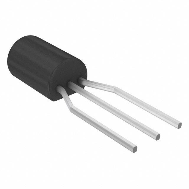
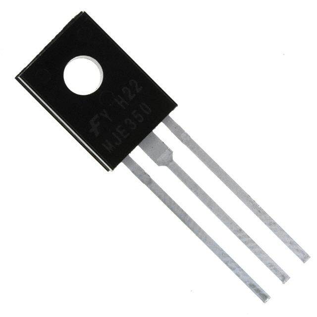
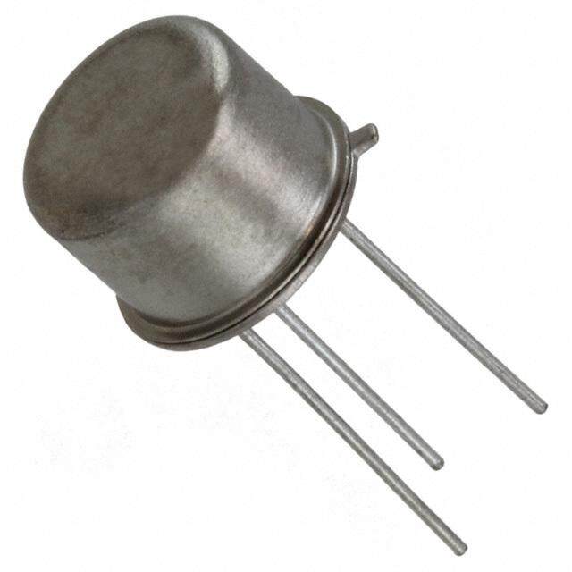
| 产品图片 |
|
| rohs | 符合RoHS无铅 / 符合限制有害物质指令(RoHS)规范要求 |
| 产品系列 | 晶体管,达林顿晶体管,ON Semiconductor MPSW45AZL1G- |
| 数据手册 | |
| 产品型号 | MPSW45AZL1G |
| 不同 Ib、Ic时的 Vce饱和值(最大值) | 1.5V @ 2mA,1A |
| 不同 Ic、Vce 时的DC电流增益(hFE)(最小值) | 25000 @ 200mA,5V |
| 产品种类 | |
| 供应商器件封装 | TO-92 |
| 其它名称 | MPSW45AZL1GOSCT |
| 功率-最大值 | 1W |
| 功率耗散 | 1 W |
| 包装 | 剪切带 (CT) |
| 发射极-基极电压VEBO | 12 V |
| 商标 | ON Semiconductor |
| 安装类型 | 通孔 |
| 安装风格 | Through Hole |
| 封装 | Ammo Pack |
| 封装/外壳 | TO-226-3,TO-92-3 长体成型引线 |
| 封装/箱体 | TO-92-3 (TO-226) |
| 工厂包装数量 | 2000 |
| 晶体管极性 | NPN |
| 晶体管类型 | NPN - 达林顿 |
| 最大工作温度 | + 150 C |
| 最大直流电集电极电流 | 1 A |
| 最大集电极截止电流 | 0.1 uA |
| 最小工作温度 | - 55 C |
| 标准包装 | 1 |
| 电压-集射极击穿(最大值) | 50V |
| 电流-集电极(Ic)(最大值) | 1A |
| 电流-集电极截止(最大值) | - |
| 直流集电极/BaseGainhfeMin | 4000, 15000, 25000 |
| 系列 | MPSW45A |
| 配置 | Single |
| 集电极—发射极最大电压VCEO | 50 V |
| 集电极—基极电压VCBO | 50 V |
| 集电极连续电流 | 1 A |
| 频率-跃迁 | 100MHz |

,TO-226_bentlead.jpg)


- 商务部:美国ITC正式对集成电路等产品启动337调查
- 曝三星4nm工艺存在良率问题 高通将骁龙8 Gen1或转产台积电
- 太阳诱电将投资9.5亿元在常州建新厂生产MLCC 预计2023年完工
- 英特尔发布欧洲新工厂建设计划 深化IDM 2.0 战略
- 台积电先进制程称霸业界 有大客户加持明年业绩稳了
- 达到5530亿美元!SIA预计今年全球半导体销售额将创下新高
- 英特尔拟将自动驾驶子公司Mobileye上市 估值或超500亿美元
- 三星加码芯片和SET,合并消费电子和移动部门,撤换高东真等 CEO
- 三星电子宣布重大人事变动 还合并消费电子和移动部门
- 海关总署:前11个月进口集成电路产品价值2.52万亿元 增长14.8%


PDF Datasheet 数据手册内容提取
MPSW45, MPSW45A One Watt Darlington Transistors NPN Silicon http://onsemi.com Features • Pb−Free Packages are Available* COLLECTOR 3 BASE MAXIMUM RATINGS 2 Rating Symbol Value Unit EMITTER 1 Collector−Emitter Voltage MPSW45 VCES 40 Vdc MPSW45A 50 Collector−Base Voltage MPSW45 VCBO 50 Vdc MPSW45A 60 Emitter−Base Voltage VEBO 12 Vdc Collector Current − Continuous IC 1.0 Adc TO−92 1 WATT Total Device Dissipation @ TA = 25°C PD 1.0 W (TO−226) Derate above 25°C 8.0 mW/°C 1 CASE 29−10 Total Device Dissipation @ TC = 25°C PD 2.5 W 123 2 3 STYLE 1 Derate above 25°C 20 mW/°C STRAIGHT LEAD BENT LEAD Operating and Storage Junction TJ, Tstg −55 to +150 °C BULK PACK TAAMPMEO & PRAECEKL Temperature Range THERMAL CHARACTERISTICS MARKING DIAGRAM Characteristic Symbol Max Unit Thermal Resistance, Junction−to−Ambient R(cid:2)JA 125 °C/W MPS Thermal Resistance, Junction−to−Case R(cid:2)JC 50 °C/W W45x AYWW(cid:2) Stresses exceeding Maximum Ratings may damage the device. Maximum (cid:2) Ratings are stress ratings only. Functional operation above the Recommended Operating Conditions is not implied. Extended exposure to stresses above the Recommended Operating Conditions may affect device reliability. MPSW45x=Device Code x = 45A Devices A =Assembly Location Y =Year WW =Work Week (cid:2) =Pb−Free Package (Note: Microdot may be in either location) ORDERING INFORMATION See detailed ordering and shipping information in the package dimensions section on page 5 of this data sheet. *For additional information on our Pb−Free strategy and soldering details, please download the ON Semiconductor Soldering and Mounting Techniques Reference Manual, SOLDERRM/D. © Semiconductor Components Industries, LLC, 2010 1 Publication Order Number: August, 2010 − Rev. 4 MPSW45/D
MPSW45, MPSW45A ELECTRICAL CHARACTERISTICS (TA = 25°C unless otherwise noted) Characteristic Symbol Min Max Unit OFF CHARACTERISTICS Collector−Emitter Breakdown Voltage V(BR)CES Vdc (IC = 100 (cid:3)Adc, VBE = 0) MPSW45 40 − MPSW45A 50 − Collector−Base Breakdown Voltage V(BR)CBO Vdc (IC = 100 (cid:3)Adc, IE = 0) MPSW45 50 − MPSW45A 60 − Emitter−Base Breakdown Voltage V(BR)EBO 12 − Vdc (IE = 10 (cid:3)Adc, IC = 0) Collector Cutoff Current ICBO nAdc (VCB = 30 Vdc, IE = 0) MPSW45 − 100 (VCB = 40 Vdc, IE = 0) MPSW45A − 100 Emitter Cutoff Current IEBO − 100 nAdc (VEB = 10 Vdc, IC = 0) ON CHARACTERISTICS (Note 1) DC Current Gain hFE − (IC = 200 mAdc, VCE = 5.0 Vdc) 25,000 150,000 (IC = 500 mAdc, VCE = 5.0 Vdc) 15,000 − (IC = 1.0 Adc, VCE = 5.0 Vdc) 4,000 − Collector−Emitter Saturation Voltage VCE(sat) − 1.5 Vdc (IC = 1.0 Adc, IB = 2.0 mAdc) Base−Emitter Saturation Voltage VBE(sat) − 2.0 Vdc (IC = 1.0 Adc, IB = 2.0 mAdc) Base−Emitter On Voltage VBE(on) − 2.0 Vdc (IC = 1.0 Adc, VCE = 5.0 Vdc) SMALL−SIGNAL CHARACTERISTICS Current−Gain − Bandwidth Product fT 100 − MHz (IC = 200 mAdc, VCE = 5.0 Vdc, f = 100 MHz) Collector−Base Capacitance Ccb − 6.0 pF (VCB = 10 Vdc, IE = 0, f = 1.0 MHz) 1. Pulse Test: Pulse Width (cid:2) 300 (cid:3)s; Duty Cycle (cid:2) 2.0%. RS in en IDEAL TRANSISTOR Figure 1. Transistor Noise Model http://onsemi.com 2
MPSW45, MPSW45A NOISE CHARACTERISTICS (V = 5.0 Vdc, T = 25°C) CE A 500 2.0 BANDWIDTH = 1.0 Hz BANDWIDTH = 1.0 Hz RS ≈ 0 1.0 200 V) A) 0.7 GE (n 100 NT (p 0.5 IC = 1.0 mA TA 10 (cid:3)A RE 0.3 OL 50 UR 0.2 OISE V 100 (cid:3)A OISE C 0.1 100 (cid:3)A e, Nn 20 IC = 1.0 mA i, Nn 00..0075 10 (cid:3)A 10 0.03 5.0 0.02 10 20 50 100200 500 1(cid:2)k 2(cid:2)k 5(cid:2)k 10(cid:2)k20(cid:2)k 50(cid:2)k 100(cid:2)k 10 20 50 100200 500 1(cid:2)k 2(cid:2)k 5(cid:2)k 10(cid:2)k 20(cid:2)k 50(cid:2)k 100(cid:2)k f, FREQUENCY (Hz) f, FREQUENCY (Hz) Figure 2. Noise Voltage Figure 3. Noise Current 200 14 V) n BANDWIDTH = 10 Hz TO 15.7 kHz E ( 12 G A BANDWIDTH = 10 Hz TO 15.7 kHz T 100 OL B) 10 E V 70 IC = 10 (cid:3)A E (d 10 (cid:3)A S R OI U 8.0 N 50 G ND E FI 100 (cid:3)A DEBA 30 100 (cid:3)A NOIS 6.0 L WI 20 NF, 4.0 IC = 1.0 mA A OT 1.0 mA 2.0 T , T V 10 0 1.0 2.0 5.0 10 20 50 100 200 500 1000 1.0 2.0 5.0 10 20 50 100 200 500 1000 RS, SOURCE RESISTANCE (kΩ) RS, SOURCE RESISTANCE (kΩ) Figure 4. Total Wideband Noise Voltage Figure 5. Wideband Noise Figure http://onsemi.com 3
MPSW45, MPSW45A SMALL−SIGNAL CHARACTERISTICS 20 4.0 N VCE = 5.0 V 10 TJ = 25°C T GAI 2.0 fT =J =1 0205 °MCHz N F) E p R CITANCE ( 57..00 Cibo Cobo GNAL CUR 10..08 PA SI A - 0.6 C, C MALL 3.0 S 0.4 |, e hf | 2.0 0.2 0.04 0.1 0.2 0.4 1.0 2.0 4.0 10 20 40 0.5 1.0 2.0 0.5 10 20 50 100 200 500 VR, REVERSE VOLTAGE (VOLTS) IC, COLLECTOR CURRENT (mA) Figure 6. Capacitance Figure 7. High Frequency Current Gain 200(cid:2)k S) 3.0 TJ = 125°C OLT TJ = 25°C V 100(cid:2)k E ( 2.5 AIN 7500(cid:2)(cid:2)kk 25°C LTAG IC = 10 mA 50 mA 250 mA 500 mA G O NT 30(cid:2)k R V 2.0 E E R T UR 20(cid:2)k MIT h, DC CFE 71.00(cid:2)(cid:2)kk -(cid:3)55°C ECTOR-E 1.5 5.0(cid:2)k VCE = 5.0 V OLL 1.0 C 3.0(cid:2)k , E 2.0(cid:2)k VC 0.5 5.0 7.0 10 20 30 50 70 100 200 300 500 0.1 0.2 0.5 1.0 2.0 5.0 10 20 50 100 200 5001000 IC, COLLECTOR CURRENT (mA) IB, BASE CURRENT ((cid:3)A) Figure 8. DC Current Gain Figure 9. Collector Saturation Region 1.6 -(cid:3)1.0 TJ = 25°C °V/C) *APPLIES FOR IC/IB ≤ hFE/3.0 25°C TO 125°C m 1.4 S ( -(cid:3)2.0 *R(cid:2)VC FOR VCE(sat) T VOLTS) 1.2 VBE(sat) @ IC/IB = 1000 FFICIEN -(cid:3)3.0 -(cid:3)55°C TO 25°C E ( OE G VBE(on) @ VCE = 5.0 V C 25°C TO 125°C LTA 1.0 RE -(cid:3)4.0 O U V, V RAT (cid:2)VB FOR VBE E P 0.8 M -(cid:3)5.0 -(cid:3)55°C TO 25°C VCE(sat) @ IC/IB = 1000 TE , V θ 0.6 R -(cid:3)6.0 5.0 7.0 10 20 30 50 70 100 200 300 500 5.0 7.0 10 20 30 50 70 100 200 300 500 IC, COLLECTOR CURRENT (mA) IC, COLLECTOR CURRENT (mA) Figure 10. “On” Voltages Figure 11. Temperature Coefficients http://onsemi.com 4
MPSW45, MPSW45A 1.0 0.7 D = 0.5 0.5 NT THERMALNORMALIZED) 00..32 0.2 0.1 0.05 SINGLE PULSE NSIENCE ( 00.0.17 SINGLE PULSE AA RT 0.05 TS r(t), RESI 0.03 ZθJC(t) = r(t) • RθJC(cid:4)TJ(pk) - TC = P(pk) ZθJC(t) 0.02 ZθJA(t) = r(t) • RθJA(cid:4)TJ(pk) - TA = P(pk) ZθJA(t) 0.01 0.1 0.2 0.5 1.0 2.0 5.0 10 20 50 100 200 500 1.0(cid:2)k 2.0(cid:2)k 5.0(cid:2)k 10(cid:2)k t, TIME (ms) Figure 12. Thermal Response 1.0(cid:2)k FIGURE A 700 1.0 ms mA) 500 tP RENT ( 320000 TA = 25°C TC = 25°C1.0 s100 (cid:3)s PP PP R U C R 100 O T 70 C LE 50 OL t1 C 30 , C CURRENT LIMIT I 20 THERMAL LIMIT 1/f SECOND BREAKDOWN LIMIT 10 DUTY(cid:2)CYCLE(cid:3)t1(cid:2)f(cid:3)t1 0.4 0.6 1.0 2.0 4.0 6.0 10 20 40 tP VCE, COLLECTOR-EMITTER VOLTAGE (VOLTS) PEAK PULSE POWER = PP Figure 13. Active Region Safe Operating Area Design Note: Use of Transient Thermal Resistance Data ORDERING INFORMATION Device Package Shipping† MPSW45G TO−92 5,000 Units / Box (Pb−Free) MPSW45RLREG TO−92 2,000 / Tape & Reel (Pb−Free) MPSW45A TO−92 5,000 Units / Box MPSW45AG TO−92 5,000 Units / Box (Pb−Free) MPSW45ARLRA TO−92 2,000 / Tape & Reel MPSW45ARLRAG TO−92 2,000 / Tape & Reel (Pb−Free) MPSW45AZL1 TO−92 2,000 / Ammo Pack MPSW45AZL1G TO−92 2,000 / Ammo Pack (Pb−Free) †For information on tape and reel specifications, including part orientation and tape sizes, please refer to our Tape and Reel Packaging Specifications Brochure, BRD8011/D. http://onsemi.com 5
MPSW45, MPSW45A PACKAGE DIMENSIONS TO−92 (TO−226) 1 WATT CASE 29−10 ISSUE O A NOTES: STRAIGHT LEAD 1. DIMENSIONING AND TOLERANCING PER ANSI BULK PACK Y14.5M, 1994. B 2. CONTROLLING DIMENSION: INCHES. R 3. CONTOUR OF PACKAGE BEYOND DIMENSION R IS UNCONTROLLED. 4. DIMENSION F APPLIES BETWEEN DIMENSIONS P P AND L. DIMENSIONS D AND J APPLY BETWEEN DI L MENSIONS L AND K MINIMUM. THE LEAD F DIMENSIONS ARE UNCONTROLLED IN DIMENSION K P AND BEYOND DIMENSION K MINIMUM. INCHES MILLIMETERS DIM MIN MAX MIN MAX A 0.175 0.205 4.44 5.21 B 0.290 0.310 7.37 7.87 X X D C 0.125 0.165 3.18 4.19 G D 0.018 0.021 0.46 0.53 H J F 0.016 0.019 0.41 0.48 G 0.045 0.055 1.15 1.39 V C HJ 00..009158 00..100254 20..4426 20..6661 SECTION X−X K 0.500 --- 12.70 --- 1 N L 0.250 --- 6.35 --- N 0.080 0.105 2.04 2.66 STYLE 1: N P --- 0.100 --- 2.54 PIN 1. EMITTER R 0.135 --- 3.43 --- 2. BASE V 0.135 --- 3.43 --- 3. COLLECTOR A NOTES: R BENT LEAD 1. DIMENSIONING AND TOLERANCING PER ASME TAPE & REEL Y14.5M, 1994. B 2. CONTROLLING DIMENSION: INCHES. AMMO PACK 3. CONTOUR OF PACKAGE BEYOND DIMENSION R IS UNCONTROLLED. 4. DIMENSION F APPLIES BETWEEN DIMENSIONS P P AND L. DIMENSIONS D AND J APPLY BETWEEN T DIMENSIONS L AND K MINIMUM. THE LEAD DIMENSIONS ARE UNCONTROLLED IN DIMENSION SPELAATNIENG K P AND BEYOND DIMENSION K MINIMUM. INCHES MILLIMETERS DIM MIN MAX MIN MAX A 0.175 0.205 4.44 5.21 B 0.290 0.310 7.37 7.87 X X D C 0.125 0.165 3.18 4.19 G D 0.018 0.021 0.46 0.53 J G 0.094 0.102 2.40 2.80 J 0.018 0.024 0.46 0.61 V K 0.500 --- 12.70 --- C N 0.080 0.105 2.04 2.66 SECTION X−X P --- 0.100 --- 2.54 1 N R 0.135 --- 3.43 --- V 0.135 --- 3.43 --- ON Semiconductor and are registered trademarks of Semiconductor Components Industries, LLC (SCILLC). SCILLC reserves the right to make changes without further notice to any products herein. SCILLC makes no warranty, representation or guarantee regarding the suitability of its products for any particular purpose, nor does SCILLC assume any liability arising out of the application or use of any product or circuit, and specifically disclaims any and all liability, including without limitation special, consequential or incidental damages. “Typical” parameters which may be provided in SCILLC data sheets and/or specifications can and do vary in different applications and actual performance may vary over time. All operating parameters, including “Typicals” must be validated for each customer application by customer’s technical experts. SCILLC does not convey any license under its patent rights nor the rights of others. SCILLC products are not designed, intended, or authorized for use as components in systems intended for surgical implant into the body, or other applications intended to support or sustain life, or for any other application in which the failure of the SCILLC product could create a situation where personal injury or death may occur. Should Buyer purchase or use SCILLC products for any such unintended or unauthorized application, Buyer shall indemnify and hold SCILLC and its officers, employees, subsidiaries, affiliates, and distributors harmless against all claims, costs, damages, and expenses, and reasonable attorney fees arising out of, directly or indirectly, any claim of personal injury or death associated with such unintended or unauthorized use, even if such claim alleges that SCILLC was negligent regarding the design or manufacture of the part. SCILLC is an Equal Opportunity/Affirmative Action Employer. This literature is subject to all applicable copyright laws and is not for resale in any manner. PUBLICATION ORDERING INFORMATION LITERATURE FULFILLMENT: N. American Technical Support: 800−282−9855 Toll Free ON Semiconductor Website: www.onsemi.com Literature Distribution Center for ON Semiconductor USA/Canada P.O. Box 5163, Denver, Colorado 80217 USA Europe, Middle East and Africa Technical Support: Order Literature: http://www.onsemi.com/orderlit Phone: 303−675−2175 or 800−344−3860 Toll Free USA/Canada Phone: 421 33 790 2910 Fax: 303−675−2176 or 800−344−3867 Toll Free USA/Canada Japan Customer Focus Center For additional information, please contact your local Email: orderlit@onsemi.com Phone: 81−3−5773−3850 Sales Representative http://onsemi.com MPSW45/D 6