ICGOO在线商城 > 分立半导体产品 > 晶体管 - 双极 (BJT) - 单 > MMBT3904WT1G
 Datasheet下载
- 型号: MMBT3904WT1G
- 制造商: ON Semiconductor
- 库位|库存: xxxx|xxxx
- 要求:
| 数量阶梯 | 香港交货 | 国内含税 |
| +xxxx | $xxxx | ¥xxxx |
查看当月历史价格
查看今年历史价格
MMBT3904WT1G产品简介:
ICGOO电子元器件商城为您提供MMBT3904WT1G由ON Semiconductor设计生产,在icgoo商城现货销售,并且可以通过原厂、代理商等渠道进行代购。 MMBT3904WT1G价格参考。ON SemiconductorMMBT3904WT1G封装/规格:晶体管 - 双极 (BJT) - 单, Bipolar (BJT) Transistor NPN 40V 200mA 300MHz 150mW Surface Mount SC-70-3 (SOT323)。您可以下载MMBT3904WT1G参考资料、Datasheet数据手册功能说明书,资料中有MMBT3904WT1G 详细功能的应用电路图电压和使用方法及教程。
MMBT3904WT1G是安森美(ON Semiconductor)生产的一款NPN型双极结型晶体管(BJT),属于通用小信号晶体管。该器件采用SOT-23小型表面贴装封装,具有体积小、响应快、可靠性高等特点,广泛应用于各类电子设备中。

其典型应用场景包括:开关电路和放大电路。在开关应用中,MMBT3904WT1G常用于驱动LED、继电器、小功率电机及逻辑控制电路中的电平转换,因其高电流增益和快速开关特性,能有效提升系统响应速度与效率。在模拟信号放大方面,适用于音频信号放大、传感器信号调理等低频小信号放大电路。

此外,该型号还广泛用于消费类电子产品(如手机、平板、智能穿戴设备)、电源管理模块、DC-DC转换器的控制电路、通信设备接口电路以及各类嵌入式系统中,作为信号切换或驱动元件。得益于其“无铅”环保设计(后缀“G”表示符合RoHS标准),也符合现代绿色电子产品的制造要求。

综上,MMBT3904WT1G凭借其高可靠性、小型化封装和良好的电气性能,成为众多电子系统中理想的通用NPN晶体管选择。
| 参数 | 数值 |
| 产品目录 | |
| 描述 | TRANS NPN 40V 200MA SOT323两极晶体管 - BJT 200mA 60V NPN |
| 产品分类 | 晶体管(BJT) - 单路分离式半导体 |
| 品牌 | ON Semiconductor |
| 产品手册 | |
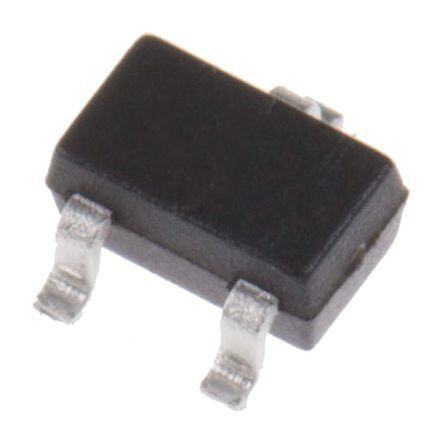
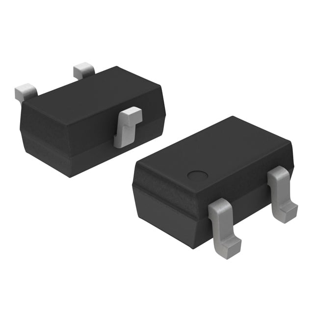
| 产品图片 |
|
| rohs | 符合RoHS无铅 / 符合限制有害物质指令(RoHS)规范要求 |
| 产品系列 | 晶体管,两极晶体管 - BJT,ON Semiconductor MMBT3904WT1G- |
| 数据手册 | |
| 产品型号 | MMBT3904WT1G |
| PCN设计/规格 | |
| 不同 Ib、Ic时的 Vce饱和值(最大值) | 300mV @ 5mA,50mA |
| 不同 Ic、Vce 时的DC电流增益(hFE)(最小值) | 100 @ 10mA,1V |
| 产品目录页面 | |
| 产品种类 | 两极晶体管 - BJT |
| 供应商器件封装 | SC-70-3(SOT323) |
| 其它名称 | MMBT3904WT1GOS |
| 功率-最大值 | 150mW |
| 包装 | 带卷 (TR) |
| 发射极-基极电压VEBO | 6 V |
| 商标 | ON Semiconductor |
| 增益带宽产品fT | 300 MHz |
| 安装类型 | 表面贴装 |
| 安装风格 | SMD/SMT |
| 封装 | Reel |
| 封装/外壳 | SC-70,SOT-323 |
| 封装/箱体 | SC-70-3 |
| 工厂包装数量 | 3000 |
| 晶体管极性 | NPN |
| 晶体管类型 | NPN |
| 最大功率耗散 | 150 mW |
| 最大工作温度 | + 150 C |
| 最大直流电集电极电流 | 0.2 A |
| 最小工作温度 | - 55 C |
| 标准包装 | 3,000 |
| 电压-集射极击穿(最大值) | 40V |
| 电流-集电极(Ic)(最大值) | 200mA |
| 电流-集电极截止(最大值) | - |
| 直流集电极/BaseGainhfeMin | 40 |
| 系列 | MMBT3904W |
| 配置 | Single |
| 集电极—发射极最大电压VCEO | 40 V |
| 集电极—基极电压VCBO | 60 V |
| 集电极—射极饱和电压 | 0.3 V |
| 集电极连续电流 | 0.2 A |
| 频率-跃迁 | 300MHz |


- 商务部:美国ITC正式对集成电路等产品启动337调查
- 曝三星4nm工艺存在良率问题 高通将骁龙8 Gen1或转产台积电
- 太阳诱电将投资9.5亿元在常州建新厂生产MLCC 预计2023年完工
- 英特尔发布欧洲新工厂建设计划 深化IDM 2.0 战略
- 台积电先进制程称霸业界 有大客户加持明年业绩稳了
- 达到5530亿美元!SIA预计今年全球半导体销售额将创下新高
- 英特尔拟将自动驾驶子公司Mobileye上市 估值或超500亿美元
- 三星加码芯片和SET,合并消费电子和移动部门,撤换高东真等 CEO
- 三星电子宣布重大人事变动 还合并消费电子和移动部门
- 海关总署:前11个月进口集成电路产品价值2.52万亿元 增长14.8%


PDF Datasheet 数据手册内容提取
MMBT3904WT1G, NPN, SMMBT3904WT1G, NPN, MMBT3906WT1G, PNP, SMMBT3906WT1G, PNP General Purpose Transistors www.onsemi.com NPN and PNP Silicon COLLECTOR 3 These transistors are designed for general purpose amplifier applications. They are housed in the SOT−323/SC−70 package which 1 is designed for low power surface mount applications. BASE Features • 2 S Prefix for Automotive and Other Applications Requiring Unique EMITTER Site and Control Change Requirements; AEC−Q101 Qualified and PPAP Capable • These Devices are Pb−Free, Halogen Free/BFR Free and are RoHS 3 SC−70 (SOT−323) Compliant 1 CASE 419 STYLE 3 2 MAXIMUM RATINGS Rating Symbol Value Unit MARKING DIAGRAM Collector−Emitter Voltage VCEO Vdc MMBT3904WT1, SMMBT3904WT1 40 MMBT3906WT1, SMMBT3906WT1 −40 xx M(cid:2) Collector−Base Voltage VCBO Vdc (cid:2) MMBT3904WT1, SMMBT3904WT1 60 MMBT3906WT1, SMMBT3906WT1 −40 1 Emitter−Base Voltage VEBO Vdc xx = AM for MMBT3904WT1, MMBT3904WT1, SMMBT3904WT1 6.0 SMMBT3904WT MMBT3906WT1, SMMBT3906WT1 −5.0 = 2A for MMBT3906WT1, SMMBT3906WT1 Collector Current − Continuous IC mAdc M = Date Code* MMBT3904WT1, SMMBT3904WT1 200 MMBT3906WT1, SMMBT3906WT1 −200 (cid:2) = Pb−Free Package (Note: Microdot may be in either location) THERMAL CHARACTERISTICS *Date Code orientation may vary depending up- Characteristic Symbol Max Unit on manufacturing location. Total Device Dissipation (Note 1) PD 150 mW @TA = 25°C ORDERING INFORMATION Thermal Resistance, Junction−to−Ambient R(cid:2)JA 833 °C/W Device Package Shipping† Junction and Storage Temperature TJ, Tstg −55 to +150 °C MMBT3904WT1G, SC−70/ 3000 / Tape & Stresses exceeding those listed in the Maximum Ratings table may damage the SMMBT3904WT1G SOT−323 Reel device. If any of these limits are exceeded, device functionality should not be assumed, damage may occur and reliability may be affected. (Pb−Free) 1. Device mounted on FR4 glass epoxy printed circuit board using the minimum MMBT3906WT1G, SC−70/ 3000 / Tape & recommended footprint. SMMBT3906WT1G SOT−323 Reel (Pb−Free) †For information on tape and reel specifications, including part orientation and tape sizes, please refer to our Tape and Reel Packaging Specifications Brochure, BRD8011/D. © Semiconductor Components Industries, LLC, 2015 1 Publication Order Number: November, 2015 − Rev. 9 MMBT3904WT1/D
MMBT3904WT1G, NPN, SMMBT3904WT1G, NPN, MMBT3906WT1G, PNP, SMMBT3906WT1G, PNP ELECTRICAL CHARACTERISTICS (TA = 25°C unless otherwise noted) Characteristic Symbol Min Max Unit OFF CHARACTERISTICS Collector−Emitter Breakdown Voltage (Note 2) V(BR)CEO Vdc (IC = 1.0 mAdc, IB = 0) MMBT3904WT1, SMMBT3904WT1 40 − (IC = −1.0 mAdc, IB = 0) MMBT3906WT1, SMMBT3906WT1 −40 − Collector−Base Breakdown Voltage V(BR)CBO Vdc (IC = 10 (cid:3)Adc, IE = 0) MMBT3904WT1, SMMBT3904WT1 60 − (IC = −10 (cid:3)Adc, IE = 0) MMBT3906WT1, SMMBT3906WT1 −40 − Emitter−Base Breakdown Voltage V(BR)EBO Vdc (IE = 10 (cid:3)Adc, IC = 0) MMBT3904WT1, SMMBT3904WT1 6.0 − (IE = −10 (cid:3)Adc, IC = 0) MMBT3906WT1, SMMBT3906WT1 −5.0 − Base Cutoff Current IBL nAdc (VCE = 30 Vdc, VEB = 3.0 Vdc) MMBT3904WT1, SMMBT3904WT1 − 50 (VCE = −30 Vdc, VEB = −3.0 Vdc) MMBT3906WT1, SMMBT3906WT1 − −50 Collector Cutoff Current ICEX nAdc (VCE = 30 Vdc, VEB = 3.0 Vdc) MMBT3904WT1, SMMBT3904WT1 − 50 (VCE = −30 Vdc, VEB = −3.0 Vdc) MMBT3906WT1, SMMBT3906WT1 − −50 ON CHARACTERISTICS (Note 2) DC Current Gain hFE − (IC = 0.1 mAdc, VCE = 1.0 Vdc) MMBT3904WT1, SMMBT3904WT1 40 − (IC = 1.0 mAdc, VCE = 1.0 Vdc) 70 − (IC = 10 mAdc, VCE = 1.0 Vdc) 100 300 (IC = 50 mAdc, VCE = 1.0 Vdc) 60 − (IC = 100 mAdc, VCE = 1.0 Vdc) 30 − (IC = −0.1 mAdc, VCE = −1.0 Vdc) MMBT3906WT1, SMMBT3906WT1 60 − (IC = −1.0 mAdc, VCE = −1.0 Vdc) 80 − (IC = −10 mAdc, VCE = −1.0 Vdc) 100 300 (IC = −50 mAdc, VCE = −1.0 Vdc) 60 − (IC = −100 mAdc, VCE = −1.0 Vdc) 30 − Collector−Emitter Saturation Voltage VCE(sat) Vdc (IC = 10 mAdc, IB = 1.0 mAdc) MMBT3904WT1, SMMBT3904WT1 − 0.2 (IC = 50 mAdc, IB = 5.0 mAdc) − 0.3 (IC = −10 mAdc, IB = −1.0 mAdc) MMBT3906WT1, SMMBT3906WT1 − −0.25 (IC = −50 mAdc, IB = −5.0 mAdc) − −0.4 Base−Emitter Saturation Voltage VBE(sat) Vdc (IC = 10 mAdc, IB = 1.0 mAdc) MMBT3904WT1, SMMBT3904WT1 0.65 0.85 (IC = 50 mAdc, IB = 5.0 mAdc) − 0.95 (IC = −10 mAdc, IB = −1.0 mAdc) MMBT3906WT1, SMMBT3906WT1 −0.65 −0.85 (IC = −50 mAdc, IB = −5.0 mAdc) − −0.95 2. Pulse Test: Pulse Width (cid:2) 300 (cid:3)s; Duty Cycle (cid:2) 2.0%. www.onsemi.com 2
MMBT3904WT1G, NPN, SMMBT3904WT1G, NPN, MMBT3906WT1G, PNP, SMMBT3906WT1G, PNP ELECTRICAL CHARACTERISTICS (TA = 25°C unless otherwise noted) (Continued) Characteristic Symbol Min Max Unit SMALL−SIGNAL CHARACTERISTICS Current−Gain − Bandwidth Product fT MHz (IC = 10 mAdc, VCE = 20 Vdc, f = 100 MHz) MMBT3904WT1, SMMBT3904WT1 300 − (IC = −10 mAdc, VCE = −20 Vdc, f = 100 MHz) MMBT3906WT1, SMMBT3906WT1 250 − Output Capacitance Cobo pF (VCB = 5.0 Vdc, IE = 0, f = 1.0 MHz) MMBT3904WT1, SMMBT3904WT1 − 4.0 (VCB = −5.0 Vdc, IE = 0, f = 1.0 MHz) MMBT3906WT1, SMMBT3906WT1 − 4.5 Input Capacitance Cibo pF (VEB = 0.5 Vdc, IC = 0, f = 1.0 MHz) MMBT3904WT1, SMMBT3904WT1 − 8.0 (VEB = −0.5 Vdc, IC = 0, f = 1.0 MHz) MMBT3906WT1, SMMBT3906WT1 − 10.0 Input Impedance hie k (cid:4) (VCE = 10 Vdc, IC = 1.0 mAdc, f = 1.0 kHz) MMBT3904WT1, SMMBT3904WT1 1.0 10 (VCE = −10 Vdc, IC = −1.0 mAdc, f = 1.0 kHz) MMBT3906WT1, SMMBT3906WT1 2.0 12 Voltage Feedback Ratio hre X 10−4 (VCE = 10 Vdc, IC = 1.0 mAdc, f = 1.0 kHz) MMBT3904WT1, SMMBT3904WT1 0.5 8.0 (VCE = −10 Vdc, IC = −1.0 mAdc, f = 1.0 kHz) MMBT3906WT1, SMMBT3906WT1 0.1 10 Small−Signal Current Gain hfe − (VCE = 10 Vdc, IC = 1.0 mAdc, f = 1.0 kHz) MMBT3904WT1, SMMBT3904WT1 100 400 (VCE = −10 Vdc, IC = −1.0 mAdc, f = 1.0 kHz) MMBT3906WT1, SMMBT3906WT1 100 400 Output Admittance hoe (cid:3)mhos (VCE = 10 Vdc, IC = 1.0 mAdc, f = 1.0 kHz) MMBT3904WT1, SMMBT3904WT1 1.0 40 (VCE = −10 Vdc, IC = −1.0 mAdc, f = 1.0 kHz) MMBT3906WT1, SMMBT3906WT1 3.0 60 Noise Figure NF dB (VCE = 5.0 Vdc, IC = 100 (cid:3)Adc, RS = 1.0 k (cid:4), f = 1.0 kHz) MMBT3904WT1, SMMBT3904WT1 − 5.0 (VCE = −5.0 Vdc, IC = −100 (cid:3)Adc, RS = 1.0 k (cid:4), f = 1.0 kHz) − 4.0 MMBT3906WT1, SMMBT3906WT1 SWITCHING CHARACTERISTICS Characteristic Condition Symbol Min Max Unit Delay Time (VCC = 3.0 Vdc, VBE = −0.5 Vdc) td 35 ns MMBT3904WT1, SMMBT3904WT1 − 35 (VCC = −3.0 Vdc, VBE = 0.5 Vdc) − MMBT3906WT1, SMMBT3906WT1 Rise Time (IC = 10 mAdc, IB1 = 1.0 mAdc) tr 35 MMBT3904WT1, SMMBT3904WT1 − 35 (IC = −10 mAdc, IB1 = −1.0 mAdc) − MMBT3906WT1, SMMBT3906WT1 Storage Time (VCC = 3.0 Vdc, IC = 10 mAdc) ts 200 ns MMBT3904WT1, SMMBT3904WT1 − 225 (VCC = −3.0 Vdc, IC = −10 mAdc) − MMBT3906WT1, SMMBT3906WT1 Fall Time (IB1 = IB2 = 1.0 mAdc) MMBT3904WT1, SMMBT3904WT1 tf − 50 (IB1 = IB2 = −1.0 mAdc) MMBT3906WT1, SMMBT3906WT1 − 75 www.onsemi.com 3
MMBT3904WT1G, NPN, SMMBT3904WT1G, NPN, MMBT3906WT1G, PNP, SMMBT3906WT1G, PNP MMBT3904WT1, SMMBT3904WT1 +3 V +3 V DUTY CYCLE = 2% 10 < t1 < 500 (cid:3)s t1 +10.9 V 300 ns +10.9 V 275 DUTY CYCLE = 2% 275 10 k 10 k 0 -(cid:2)0.5 V < 1 ns CS < 4 pF* 1N916 CS < 4 pF* -(cid:2)9.1 V < 1 ns * Total shunt capacitance of test jig and connectors Figure 1. Delay and Rise Time Figure 2. Storage and Fall Time Equivalent Test Circuit Equivalent Test Circuit www.onsemi.com 4
MMBT3904WT1G, NPN, SMMBT3904WT1G, NPN, MMBT3906WT1G, PNP, SMMBT3906WT1G, PNP MMBT3904WT1, SMMBT3904WT1 TYPICAL TRANSIENT CHARACTERISTICS TJ = 25°C TJ = 125°C 500 500 300 IC/IB = 10 300 VCC = 40 V 200 200 IC/IB = 10 100 100 s) ns) 7500 tr @ VCC = 3.0 V ME (n 7500 ME ( E TI TI 30 40 V RIS 30 20 t , r 20 15 V 10 MMBT3904WT1 10 MMBT3904WT1 7 td @ VOB = 0 V 2.0 V 7 5 5 1.0 2.0 3.0 5.0 7.0 10 20 30 50 70 100 200 1.0 2.0 3.0 5.0 7.0 10 20 30 50 70 100 200 IC, COLLECTOR CURRENT (mA) IC, COLLECTOR CURRENT (mA) Figure 3. Turn−On Time Figure 4. Rise Time 500 500 300 t′s = ts - 1/8 tf 300 VCC = 40 V 200 IC/IB = 20 IC/IB = 10 IB1 = IB2 200 IB1 = IB2 IC/IB = 20 ns) 100 s) 100 ME ( 70 E (n 70 STORAGE TI 532000 IC/IB =IC 2/I0B = 10 t , FALL TIMf 532000 IC/IB = 10 ′t , s 10 10 MMBT3904WT1 MMBT3904WT1 7 7 5 5 200 1.0 2.0 3.0 5.0 7.0 10 20 30 50 70 100 200 1.0 2.0 3.0 5.0 7.0 10 20 30 50 70 100 IC, COLLECTOR CURRENT (mA) IC, COLLECTOR CURRENT (mA) Figure 5. Storage Time Figure 6. Fall Time TYPICAL AUDIO SMALL−SIGNAL CHARACTERISTICS NOISE FIGURE VARIATIONS (V = 5.0 Vdc, T = 25°C, Bandwidth = 1.0 Hz) CE A 12 14 SOURCE RESISTANCE = 200 (cid:4) f = 1.0 kHz 10 IC = 1.0 mA 12 IC = 1.0 mA URE (dB) 8 SICO =U 0R.5C Em ARESISTANCE = 200 (cid:4) URE (dB) 180 IC = 0.5 mA IC = 50 (cid:3)A G G E FI 6 SOURCE RESISTANCE = 1.0 k E FI IC = 100 (cid:3)A OIS IC = 50 (cid:3)A OIS 6 N N NF, 4 NF, 4 2 SOURCE RESISTANCE = 500 (cid:4) 2 IC = 100 (cid:3)A MMBT3904WT1 MMBT3904WT1 0 0 0.1 0.2 0.4 1.0 2.0 4.0 10 20 40 100 0.1 0.2 0.4 1.0 2.0 4.0 10 20 40 100 f, FREQUENCY (kHz) RS, SOURCE RESISTANCE (k OHMS) Figure 7. Noise Figure Figure 8. Noise Figure www.onsemi.com 5
MMBT3904WT1G, NPN, SMMBT3904WT1G, NPN, MMBT3906WT1G, PNP, SMMBT3906WT1G, PNP MMBT3904WT1, SMMBT3904WT1 h PARAMETERS (V = 10 Vdc, f = 1.0 kHz, T = 25°C) CE A 300 100 s) MMBT3904WT1 ho 50 MMBT3904WT1 m 200 (cid:3)E ( AIN ANC 20 G T RENT 100 ADMIT 10 R T U U C 70 P 5 h , fe OUT 50 h , oe 2 30 1 0.1 0.2 0.3 0.5 1.0 2.0 3.0 5.0 10 0.1 0.2 0.3 0.5 1.0 2.0 3.0 5.0 10 IC, COLLECTOR CURRENT (mA) IC, COLLECTOR CURRENT (mA) Figure 9. Current Gain Figure 10. Output Admittance 20 10 S) 10 MMBT3904WT1 10 )-4 7.0 MMBT3904WT1 M X OH O ( 5.0 E (k 5.0 RATI NC CK 3.0 MPEDA 2.0 EEDBA 2.0 UT I 1.0 E F P G N A h , Iie 0.5 h , VOLTre 10..07 0.2 0.5 0.1 0.2 0.3 0.5 1.0 2.0 3.0 5.0 10 0.1 0.2 0.3 0.5 1.0 2.0 3.0 5.0 10 IC, COLLECTOR CURRENT (mA) IC, COLLECTOR CURRENT (mA) Figure 11. Input Impedance Figure 12. Voltage Feedback Ratio TYPICAL STATIC CHARACTERISTICS 1000 VCE = 1 V N TJ = 150°C AI T G 25°C N E R -(cid:2)55°C R U 100 C C D , E F h MMBT3904WT1 10 1.0 10 100 1000 IC, COLLECTOR CURRENT (mA) Figure 13. DC Current Gain www.onsemi.com 6
MMBT3904WT1G, NPN, SMMBT3904WT1G, NPN, MMBT3906WT1G, PNP, SMMBT3906WT1G, PNP MMBT3904WT1, SMMBT3904WT1 TS) 1.0 L VO MMBT3904WT1 TJ = 25°C E ( G 0.8 TA IC = 1.0 mA 10 mA 30 mA 100 mA L O V R 0.6 E T T MI E R 0.4 O T C E L OL 0.2 C V , CE 0 0.01 0.02 0.03 0.05 0.07 0.1 0.2 0.3 0.5 0.7 1.0 2.0 3.0 5.0 7.0 10 IB, BASE CURRENT (mA) Figure 14. Collector Saturation Region 0.9 1.4 , COLLECTOR−EMITTERE(sat)SATURATION VOLTAGE (V)0000000.......3457826 IC/IB = 10 25°C150°C−55°C V, BASE−EMITTERBE(sat)SATURATION VOLTAGE (V) 00011.....46802 −1255550°°°ICCCC/IB = 10 VC 0.1 0 0.2 0.001 0.01 0.1 1 0.0001 0.001 0.01 0.1 1 IC, COLLECTOR CURRENT (A) IC, COLLECTOR CURRENT (A) Figure 15. Collector Emitter Saturation Voltage Figure 16. Base Emitter Saturation Voltage vs. vs. Collector Current Collector Current 1.4 V) E ( VCE = 1 V G 1.2 A T L O V 1.0 R E −55°C T T 0.8 MI E 25°C − E 0.6 S A B , n) 0.4 150°C o E( B V 0.2 0.0001 0.001 0.01 0.1 1 IC, COLLECTOR CURRENT (A) Figure 17. Base Emitter Voltage vs. Collector Current www.onsemi.com 7
MMBT3904WT1G, NPN, SMMBT3904WT1G, NPN, MMBT3906WT1G, PNP, SMMBT3906WT1G, PNP MMBT3904WT1, SMMBT3904WT1 TJ = 25°C TJ = 125°C 1.0 10 MMBT3904WT1 MMBT3904WT1 0.5 +25°C TO +125°C 7.0 °mV/ C) 0 (cid:2)VC FOR VCE(sat) -(cid:2)55°C TO +25°C E (pF) 5.0 NT ( ANC Cibo CIE -(cid:2)0.5 CIT 3.0 COEFFI -(cid:2)1.0 +-2(cid:2)555°°CC T TOO + +12255°°CC CAPA 2.0 Cobo -(cid:2)1.5 (cid:2)VB FOR VBE(sat) -(cid:2)2.0 1.0 0 20 40 60 80 100 120 140 160 180 200 0.1 0.2 0.3 0.5 0.7 1.0 2.0 3.0 5.07.010 20 30 40 IC, COLLECTOR CURRENT (mA) REVERSE BIAS VOLTAGE (VOLTS) Figure 18. Temperature Coefficients Figure 19. Capacitance 1000 1 100 mS 10 mS WIDTH VTAC E= =2 51° CV T (A) 1 mS D N 1 S AIN−BANCT (MHz)100 R CURRE 0.1 GU O −D T Thermal Limit TO C NR E 0.01 REP LL R O U C , CT I, C f 10 0.001 0.1 1 10 100 1000 0.1 1 10 100 IC, COLLECTOR CURRENT (mA) VCE, COLLECTOR EMITTER VOLTAGE (V) Figure 20. Current Gain Bandwidth Product Figure 21. Safe Operating Area vs. Collector Current www.onsemi.com 8
MMBT3904WT1G, NPN, SMMBT3904WT1G, NPN, MMBT3906WT1G, PNP, SMMBT3906WT1G, PNP MMBT3906WT1, SMMBT3906WT1 3 V 3 V < 1 ns +(cid:2)9.1 V 275 275 < 1 ns 10 k 10 k 0 CS < 4 pF* 1N916 CS < 4 pF* +10.6 V DUTY 3C0Y0C nLsE = 2% 10 < t1 < 500 (cid:3)s t1 10.9 V DUTY CYCLE = 2% * Total shunt capacitance of test jig and connectors Figure 22. Delay and Rise Time Figure 23. Storage and Fall Time Equivalent Test Circuit Equivalent Test Circuit TYPICAL TRANSIENT CHARACTERISTICS TJ = 25°C TJ = 125°C 500 500 300 MMBT3906WT1 IC/IB = 10 300 MMBT3906WT1 VCC = 40 V 200 200 IB1 = IB2 IC/IB = 20 100 s) 100 n E (ns) 7500 tr @ VCC = 3.0 V LL TIME ( 7500 TIM 3200 15 V t , FAf 3200 IC/IB = 10 40 V 10 2.0 V 10 7 7 td @ VOB = 0 V 5 5 1.0 2.0 3.0 5.0 7.0 10 20 30 50 70 100 200 1.0 2.0 3.0 5.0 7.0 10 20 30 50 70 100 200 IC, COLLECTOR CURRENT (mA) IC, COLLECTOR CURRENT (mA) Figure 24. Turn−On Time Figure 25. Fall Time TYPICAL AUDIO SMALL−SIGNAL CHARACTERISTICS NOISE FIGURE VARIATIONS (V = −5.0 Vdc, T = 25°C, Bandwidth = 1.0 Hz) CE A 5.0 12 SOURCE RESISTANCE = 200 (cid:4) f = 1.0 kHz IC = 1.0 mA IC = 1.0 mA 10 4.0 B) SOURCE RESISTANCE = 200 (cid:4) B) IC = 0.5 mA E (d IC = 0.5 mA E (d 8.0 R 3.0 R U U G SOURCE RESISTANCE = 2.0 k G E FI IC = 50 (cid:3)A E FI 6.0 OIS 2.0 OIS F, N F, N 4.0 IC = 50 (cid:3)A N N 1.0 SICO =U 1R0C0E (cid:3) RAESISTANCE = 2.0 k 2.0 IC = 100 (cid:3)A MMBT3906WT1 MMBT3906WT1 0 0 0.1 0.2 0.4 1.0 2.0 4.0 10 20 40 100 0.1 0.2 0.4 1.0 2.0 4.0 10 20 40 100 f, FREQUENCY (kHz) RS, SOURCE RESISTANCE (k(cid:4)) Figure 26. Figure 27. www.onsemi.com 9
MMBT3904WT1G, NPN, SMMBT3904WT1G, NPN, MMBT3906WT1G, PNP, SMMBT3906WT1G, PNP MMBT3906WT1, SMMBT3906WT1 h PARAMETERS (V = −10 Vdc, f = 1.0 kHz, T = 25°C) CE A 300 100 MMBT3906WT1 os) 70 MMBT3906WT1 h m 50 200 (cid:3)E ( N C AI N 30 G A T TT REN 100 DMI 20 UR T A C 70 U , e TP hf 50 OU 10 h , oe 7.0 30 5.0 0.1 0.2 0.3 0.5 0.7 1.0 2.0 3.0 5.0 7.0 10 0.1 0.2 0.3 0.5 0.7 1.0 2.0 3.0 5.0 7.0 10 IC, COLLECTOR CURRENT (mA) IC, COLLECTOR CURRENT (mA) Figure 28. Current Gain Figure 29. Output Admittance 20 10 10 MMBT3906WT1 0 )-4 7.0 MMBT3906WT1 1 ΩANCE (k ) 375...000 K RATIO (X 35..00 D 2.0 C PE BA 2.0 M D UT I 1.0 FEE h , INPie 00..75 OLTAGE 1.0 V 0.7 00..32 h , re 0.5 0.1 0.2 0.3 0.5 0.7 1.0 2.0 3.0 5.0 7.0 10 0.1 0.2 0.3 0.5 0.7 1.0 2.0 3.0 5.0 7.0 10 IC, COLLECTOR CURRENT (mA) IC, COLLECTOR CURRENT (mA) Figure 30. Input Impedance Figure 31. Voltage Feedback Ratio STATIC CHARACTERISTICS 1000 VCE = 1 V N TJ = 150°C AI G 25°C T N E RR -(cid:2)55°C U 100 C C D , E F h MMBT3906WT1 10 1.0 10 100 1000 IC, COLLECTOR CURRENT (mA) Figure 32. DC Current Gain www.onsemi.com 10
MMBT3904WT1G, NPN, SMMBT3904WT1G, NPN, MMBT3906WT1G, PNP, SMMBT3906WT1G, PNP MMBT3906WT1, SMMBT3906WT1 S) 1.0 T VOL MMBT3906WT1 TJ = 25°C E ( 0.8 G TA IC = 1.0 mA 10 mA 30 mA 100 mA L O V R 0.6 E T T MI R E 0.4 O T C E LL 0.2 O C V , CE 0 0.01 0.02 0.03 0.05 0.07 0.1 0.2 0.3 0.5 0.7 1.0 2.0 3.0 5.0 7.0 10 IB, BASE CURRENT (mA) Figure 33. Collector Saturation Region 0.50 1.4 R 0.45 IC/IB = 10 IC/IB = 10 , COLLECTOR−EMITTEE(sat)SATURATION VOLTAGE (V)0000000.......12241335050005 25°C 150°C−55°C V, BASE−EMITTERBE(sat)SATURATION VOLTAGE (V) 00011.....46802 1−525055°°CC°C C V 0.05 0 0.2 0.001 0.01 0.1 1 0.0001 0.001 0.01 0.1 1 IC, COLLECTOR CURRENT (A) IC, COLLECTOR CURRENT (A) Figure 34. Collector Emitter Saturation Voltage Figure 35. Base Emitter Saturation Voltage vs. vs. Collector Current Collector Current 1.4 V) E ( VCE = 1 V G 1.2 A T L O V 1.0 R TE −55°C T 0.8 MI E 25°C − E 0.6 S A B , n) 0.4 150°C o E( B V 0.2 0.0001 0.001 0.01 0.1 1 IC, COLLECTOR CURRENT (A) Figure 36. Base Emitter Voltage vs. Collector Current www.onsemi.com 11
MMBT3904WT1G, NPN, SMMBT3904WT1G, NPN, MMBT3906WT1G, PNP, SMMBT3906WT1G, PNP MMBT3906WT1, SMMBT3906WT1 TJ = 25°C TJ = 125°C 1.0 10 °C) MMBT3906WT1 V/ 7.0 m 0.5 S ( (cid:2)VC FOR VCE(sat) +25°C TO +125°C T EFFICIEN 0 -(cid:2)55°C TO +25°C NCE (pF) 5.0 CCobiboo RE CO -0.5 MMBT3906WT1 +25°C TO +125°C PACITA 3.0 ERATU -1.0 (cid:2)VS FOR VBE(sat) -(cid:2)55°C TO +25°C CA 2.0 P M -1.5 E T , V θ -2.0 1.0 0 20 40 60 80 100 120 140 160 180 200 0.1 0.2 0.3 0.5 0.7 1.0 2.0 3.0 5.07.010 20 30 40 IC, COLLECTOR CURRENT (mA) REVERSE BIAS VOLTAGE (VOLTS) Figure 37. Temperature Coefficients Figure 38. Capacitance 1000 1 100 mS 10 mS WIDTH VTAC E= =2 51° CV T (A) D N 1 mS AIN−BANCT (MHz)100 R CURRE 0.1 1 S GU O −D T Thermal Limit TO C NR E 0.01 REP LL R O U C , CT I, C f 10 0.001 0.1 1 10 100 1000 0.1 1 10 100 IC, COLLECTOR CURRENT (mA) VCE, COLLECTOR EMITTER VOLTAGE (V) Figure 39. Current Gain Bandwidth Product Figure 40. Safe Operating Area vs. Collector Current www.onsemi.com 12
MMBT3904WT1G, NPN, SMMBT3904WT1G, NPN, MMBT3906WT1G, PNP, SMMBT3906WT1G, PNP PACKAGE DIMENSIONS SC−70 (SOT−323) CASE 419−04 ISSUE N D NOTES: 1. DIMENSIONING AND TOLERANCING PER ANSI Y14.5M, 1982. e1 2. CONTROLLING DIMENSION: INCH. MILLIMETERS INCHES 3 DIM MIN NOM MAX MIN NOM MAX A 0.80 0.90 1.00 0.032 0.035 0.040 HE E A1 0.00 0.05 0.10 0.000 0.002 0.004 1 2 A2 0.70 REF 0.028 REF b 0.30 0.35 0.40 0.012 0.014 0.016 c 0.10 0.18 0.25 0.004 0.007 0.010 D 1.80 2.10 2.20 0.071 0.083 0.087 b E 1.15 1.24 1.35 0.045 0.049 0.053 e 1.20 1.30 1.40 0.047 0.051 0.055 e e1 0.65 BSC 0.026 BSC L 0.20 0.38 0.56 0.008 0.015 0.022 HE 2.00 2.10 2.40 0.079 0.083 0.095 c STYLE 3: A A2 PIN 1.BASE 2.EMITTER 3.COLLECTOR 0.05 (0.002) L A1 SOLDERING FOOTPRINT* 0.65 0.65 0.025 0.025 1.9 0.075 0.9 0.035 0.7 0.028 (cid:3) (cid:4) mm SCALE 10:1 inches *For additional information on our Pb−Free strategy and soldering details, please download the ON Semiconductor Soldering and Mounting Techniques Reference Manual, SOLDERRM/D. ON Semiconductor and are registered trademarks of Semiconductor Components Industries, LLC (SCILLC). SCILLC reserves the right to make changes without further notice to any products herein. SCILLC makes no warranty, representation or guarantee regarding the suitability of its products for any particular purpose, nor does SCILLC assume any liability arising out of the application or use of any product or circuit, and specifically disclaims any and all liability, including without limitation special, consequential or incidental damages. “Typical” parameters which may be provided in SCILLC data sheets and/or specifications can and do vary in different applications and actual performance may vary over time. All operating parameters, including “Typicals” must be validated for each customer application by customer’s technical experts. SCILLC does not convey any license under its patent rights nor the rights of others. SCILLC products are not designed, intended, or authorized for use as components in systems intended for surgical implant into the body, or other applications intended to support or sustain life, or for any other application in which the failure of the SCILLC product could create a situation where personal injury or death may occur. Should Buyer purchase or use SCILLC products for any such unintended or unauthorized application, Buyer shall indemnify and hold SCILLC and its officers, employees, subsidiaries, affiliates, and distributors harmless against all claims, costs, damages, and expenses, and reasonable attorney fees arising out of, directly or indirectly, any claim of personal injury or death associated with such unintended or unauthorized use, even if such claim alleges that SCILLC was negligent regarding the design or manufacture of the part. SCILLC is an Equal Opportunity/Affirmative Action Employer. This literature is subject to all applicable copyright laws and is not for resale in any manner. PUBLICATION ORDERING INFORMATION LITERATURE FULFILLMENT: N. American Technical Support: 800−282−9855 Toll Free ON Semiconductor Website: www.onsemi.com Literature Distribution Center for ON Semiconductor USA/Canada P.O. Box 5163, Denver, Colorado 80217 USA Europe, Middle East and Africa Technical Support: Order Literature: http://www.onsemi.com/orderlit Phone: 303−675−2175 or 800−344−3860 Toll Free USA/Canada Phone: 421 33 790 2910 Fax: 303−675−2176 or 800−344−3867 Toll Free USA/Canada Japan Customer Focus Center For additional information, please contact your local Email: orderlit@onsemi.com Phone: 81−3−5817−1050 Sales Representative www.onsemi.com MMBT3904WT1/D 13
Mouser Electronics Authorized Distributor Click to View Pricing, Inventory, Delivery & Lifecycle Information: O N Semiconductor: MMBT3904WT1G MMBT3906WT1G SMMBT3904WT1G