ICGOO在线商城 > 传感器,变送器 > 运动传感器 - 加速计 > MMA8491QR1
 Datasheet下载
- 型号: MMA8491QR1
- 制造商: Freescale Semiconductor
- 库位|库存: xxxx|xxxx
- 要求:
| 数量阶梯 | 香港交货 | 国内含税 |
| +xxxx | $xxxx | ¥xxxx |
查看当月历史价格
查看今年历史价格
MMA8491QR1产品简介:
ICGOO电子元器件商城为您提供MMA8491QR1由Freescale Semiconductor设计生产,在icgoo商城现货销售,并且可以通过原厂、代理商等渠道进行代购。 MMA8491QR1价格参考¥21.13-¥21.13。Freescale SemiconductorMMA8491QR1封装/规格:运动传感器 - 加速计, Accelerometer X, Y, Z Axis ±8g 0.5Hz ~ 400Hz 12-QFN (3x3)。您可以下载MMA8491QR1参考资料、Datasheet数据手册功能说明书,资料中有MMA8491QR1 详细功能的应用电路图电压和使用方法及教程。
NXP USA Inc. 的 MMA8491QR1 是一款三轴低功耗加速度传感器,广泛应用于需要精确运动检测和低功耗的场景。以下是其主要应用场景:

 1. 消费电子设备
   - 智能手机和平板电脑:用于屏幕方向检测(自动旋转)、计步器功能、手势识别等。
   - 可穿戴设备:如智能手环或手表,实现活动跟踪、睡眠监测、跌倒检测等功能。
   - 游戏控制器:通过检测用户的动作来控制游戏中的角色或操作。

 2. 工业自动化
   - 振动监测:用于监控机械设备的振动情况,预测潜在故障。
   - 倾斜检测:在机器人、无人机或其他自动化设备中,用于保持平衡或调整姿态。
   - 冲击检测:在运输过程中保护贵重物品,记录是否发生剧烈震动或撞击。

 3. 汽车电子
   - 安全气囊系统:检测碰撞时的加速度变化,触发安全气囊展开。
   - 导航系统:结合 GPS 提供更精准的位置信息,尤其是在信号弱的情况下。
   - 车辆状态监测:用于检测车辆倾斜角度或判断是否发生侧翻。

 4. 健康与医疗
   - 病人监护:监测患者的活动水平、步态分析或跌倒报警。
   - 康复训练:帮助患者进行正确的动作练习,并记录数据以评估恢复进度。

 5. 物联网 (IoT)
   - 智能家居:用于检测门窗开关状态、入侵报警或家具移动。
   - 资产追踪:在物流领域,实时监测货物的状态和位置。

MMA8491QR1 的低功耗特性使其非常适合电池供电的设备,而其高灵敏度和小尺寸则为设计提供了更大的灵活性。这些特点使其成为众多应用领域的理想选择。
| 参数 | 数值 |
| 产品目录 | |
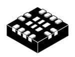
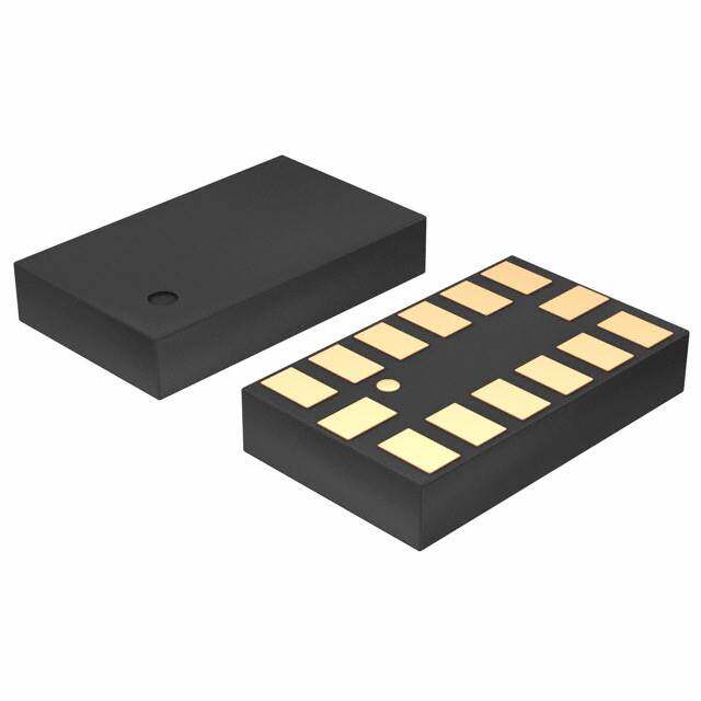
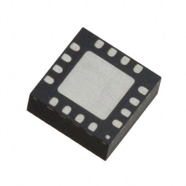
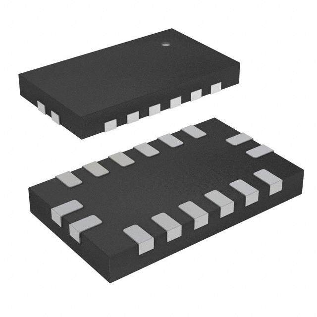
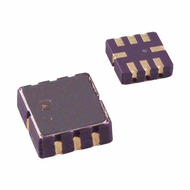
| 描述 | IC ACCELEROMETER 3AXIS 12QFN加速计 3-Axis Low Voltage Discrete Tilt Sensor |
| 产品分类 | 加速计运动与定位传感器 |
| 品牌 | Freescale Semiconductor |
| 产品手册 | |
| 产品图片 |
|
| rohs | RoHS 合规性豁免含铅 / 不受限制有害物质指令(RoHS)规范要求限制 |
| 产品系列 | 加速计,Freescale Semiconductor MMA8491QR1- |
| 数据手册 | |
| 产品型号 | MMA8491QR1 |
| PCN设计/规格 | http://cache.freescale.com/files/shared/doc/pcn/PCN15613.htm |
| 产品种类 | 加速计 |
| 传感轴 | Triple |
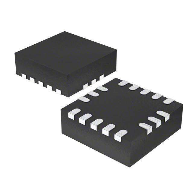
| 供应商器件封装 | 12-QFN(3x3) |
| 其它名称 | MMA8491QR1DKR |
| 分辨率 | 14 bit |
| 加速 | 8 g |
| 加速度范围 | ±8g |
| 单位重量 | 20.100 mg |
| 商标 | Freescale Semiconductor |
| 商标名 | Xtrinsic |
| 安装类型 | 表面贴装 |
| 安装风格 | SMD/SMT |
| 封装 | Reel |
| 封装/外壳 | 12-TQFN 裸露焊盘 |
| 封装/箱体 | QFN-12 |
| 工厂包装数量 | 1000 |
| 带宽 | 800Hz |
| 接口 | I²C |
| 数字输出-位数 | 14 bit |
| 数字输出-总线接口 | I2C |
| 最大工作温度 | + 85 C |
| 最小工作温度 | - 40 C |
| 标准包装 | 1 |
| 灵敏度 | 1024计数/g |
| 特色产品 | http://www.digikey.cn/product-highlights/cn/zh/freescale-mma8491q-xtrinsic-accelerometer/3562 |
| 电压-电源 | 1.95 V ~ 3.6 V |
| 电源电压-最大 | 3.6 V |
| 电源电压-最小 | 1.95 V |
| 系列 | MMA8491Q |
| 轴 | X,Y,Z |
| 输出类型 | I²C |


- 商务部:美国ITC正式对集成电路等产品启动337调查
- 曝三星4nm工艺存在良率问题 高通将骁龙8 Gen1或转产台积电
- 太阳诱电将投资9.5亿元在常州建新厂生产MLCC 预计2023年完工
- 英特尔发布欧洲新工厂建设计划 深化IDM 2.0 战略
- 台积电先进制程称霸业界 有大客户加持明年业绩稳了
- 达到5530亿美元!SIA预计今年全球半导体销售额将创下新高
- 英特尔拟将自动驾驶子公司Mobileye上市 估值或超500亿美元
- 三星加码芯片和SET,合并消费电子和移动部门,撤换高东真等 CEO
- 三星电子宣布重大人事变动 还合并消费电子和移动部门
- 海关总署:前11个月进口集成电路产品价值2.52万亿元 增长14.8%

PDF Datasheet 数据手册内容提取
MMA8491Q 3-Axis Multifunction Digital Accelerometer Rev. 2.1 — 26 April 2016 Data sheet: Technical data COMPANY PUBLIC 1 General description The MMA8491Q is a low voltage, 3-axis low-g accelerometer housed in a 3 mm x 3 mm QFN package. The device can accommodate two accelerometer configurations, acting 2 as either a 45° tilt sensor or a digital output accelerometer with I C bus. • As a 45° tilt sensor, the MMA8491Q device offers extreme ease of implementation by using a single line output per axis. • As a digital output accelerometer, the 14-bit ±8 g accelerometer data can be read from the device with a 1 mg/LSB sensitivity. The extreme low power capabilities of the MMA8491Q will reduce the low data rate current consumption to less than 400 nA per Hz. 2 Features and benefits • Extreme low power, 400 nA per Hz • Ultra-fast data output time, ~700 μs • V supply range of 1.95 V to 3.6 V DD • 3 mm x 3 mm, 0.65 mm pitch with visual solder joint inspection • ±8 g full-scale range • 14-bit digital output, 1 mg/LSB sensitivity 1 • Output Data Rate (ODR), implementation based from < 1 Hz to 800 Hz 2 • I C digital interface • 3-axis, 45° tilt outputs 3 Typical applications • Smart grid: tamper detect • Anti-theft • White goods tilt • Remote controls 1 The ODR for this device is user defined by the period of the Enable pulsed signal. The maximum recommended frequency of the Enable signal or the ODR that can be achieved for this device is 800 Hz.
NXP Semiconductors MMA8491Q 3-Axis Multifunction Digital Accelerometer 4 Ordering information Table 1. Ordering information Part Number Temperature Range Package Shipping MMA8491QT –40 to +85 °C QFN 12 Tray MMA8491QR1 –40 to +85 °C QFN 12 1000 pc / Tape & Reel MMA8491QR2 –40 to +85 °C QFN 12 5000 pc / Tape & Reel 5 Related documentation The MMA8491Q device features and operations are described in a variety of reference manuals, user guides, and application notes. To find the most current versions of these documents: 1. Go to the NXP homepage at: http://www.nxp.com/ 2. In the Keyword search box at the top of the page, enter the device number MMA8491Q. In the Refine Your Result pane on the left, click on the Documentation link. 6 Block diagram Figure 1. Block Diagram 7 Pinout MMA8491Q is hosted in a 12-pin 3 mm x 3 mm QFN package. Ten pins are used for functions; two pins are unconnected. Refer to Table 2 for complete pin descriptions and functions. MMA8491Q All information provided in this document is subject to legal disclaimers. © NXP B.V. 2016. All rights reserved Data sheet: Technical data Rev. 2.1 — 26 April 2016 COMPANY PUBLIC 2 / 28
NXP Semiconductors MMA8491Q 3-Axis Multifunction Digital Accelerometer MMA8491Q C C N N 2 1 1 1 Byp 1 10 Xout V 2 9 Yout DD SDA 3 8 Zout EN 4 7 Gnd 5 6 L d C n S G Transparent top view Figure 2. Pin connection diagram Table 2. Pin descriptions Pin Symbol Function Description Pin status 1 Byp Internal regulator The internal regulator voltage of 1.8 V is present on this Output output capacitor pin. Connect to external 0.1 μF bypass capacitor. connection 2 V Power Supply Device power is supplied through the V line. Power Input DD DD supply decoupling capacitors should be placed as near as possible to pin 1 of the device. 2 2 3 SDA I C Data I C Slave Data Line, open drain Input/Output 2 • 7-bit I C device address is 0x55 2 • The SDA and SCL I C connections are open drain, and therefore usually require a pull-up resistor 4 EN Enable pin The Enable pin fully turns on the accelerometer system Input when it is pulled up to logic high. The accelerometer system is turned off when the Enable pin is logic low. 2 2 5 SCL I C Clock I C Slave Clock Line, open drain Input 6 Gnd Ground Ground Ground 7 Gnd Ground Ground Ground 8 Zout Push-pull Z-Axis • Output is high when acceleration is > 0.688 g (axis is | Output Tilt Detection φ| > 45°). Output • Output is low when acceleration is ≤ 0.688 g (axis is |φ| ≤ 45°). 9 Yout Push-pull Y-Axis Output Tilt Detection • These pins are push-pull output pins. Output 10 Xout Push-pull X-Axis Output Tilt Detection Output 11 NC No internal No internal connection connection 12 NC No internal No internal connection connection MMA8491Q All information provided in this document is subject to legal disclaimers. © NXP B.V. 2016. All rights reserved Data sheet: Technical data Rev. 2.1 — 26 April 2016 COMPANY PUBLIC 3 / 28
NXP Semiconductors MMA8491Q 3-Axis Multifunction Digital Accelerometer 8 Recommended application diagram Figure 3. V connects to power supply and EN is pulsed DD To ensure the accelerometer is fully functional, connect the MMA8491Q as suggested in Figure 3. • A capacitor must be connected to the Bypass pin (pin 1) to assist the internal voltage regulator. It is recommended to use a 0.1 μF capacitor. The capacitor should be placed as near as possible to the Bypass pin. • The device power is supplied through the V line. The power supply decoupling DD capacitor should be placed as close as possible to the V pin. DD –Use a 1.0 or 4.7 μF capacitor when the V and EN are not tied together. DD –When V and EN are tied together, use a 0.1 μF capacitor. The 0.1 μF capacitor DD value has been chosen to minimize the average current consumption while still maintaining an acceptable level of power supply high frequency filtering. • Both ground pins (pins 6 and 7) must be connected to ground. 2 • When the I C communication line is used, use a pull-up resistor to connect to line SDA and SCL. The SCL line can be driven by a push-pull driver, in which case, no pull-up resistor is necessary. If SDA and SCL pins are not used, then they should be tied to ground. 9 Sensing direction and output response The MMA8491Q has three tilt detection outputs: Xout, Yout, and Zout. The following figure shows the output results at the six different orientation positions. MMA8491Q All information provided in this document is subject to legal disclaimers. © NXP B.V. 2016. All rights reserved Data sheet: Technical data Rev. 2.1 — 26 April 2016 COMPANY PUBLIC 4 / 28
NXP Semiconductors MMA8491Q 3-Axis Multifunction Digital Accelerometer Top view Side view Portrait Up Back Pin 1 Xout @ 0g Gravity Yout @ 0g Zout @ –1g Xout @ 0g Yout @ –1g Front Landscape Left Zout @ 0g Landscape Right Xout @ 0g Yout @ 0g Zout @ 1g Xout @ –1g Xout @ 1g Z Yout @ 0g Yout @ 0g Zout @ 0g Portrait Down Zout @ 0g X Y Xout @ 0g Yout @ 1g (Top view) Zout @ 0g Reference frame for acceleration measurement Figure 4. Sensitive axes orientation and output response to ±1 g (gravity) stimulus 10 Mechanical and electrical specifications 10.1 Absolute maximum ratings Absolute maximum ratings are the limits the device can be exposed to without damage. Functional operation at absolute maximum rating is not guaranteed. Although this device contains circuitry to protect against damage due to high static voltage or electrostatic fields, it is advised that normal precautions be taken to avoid application of any voltage higher than the maximum-rated voltage. Table 3. Absolute maximum ratings Symbol Rating Min Max Unit g Maximum acceleration (all axes, 100 μs) — 10 000 V max V Analog supply voltage –0.3 3.6 V DD D Drop test — 1.8 m drop T Operating temperature –40 +85 °C AGOC T Storage temperature –40 +125 °C STG Table 4. ESD and latch-up protection characteristics Symbol Rating Value Unit V Human body model (HBM) ±2000 V HBM V Machine model (MM) ±200 V MM MMA8491Q All information provided in this document is subject to legal disclaimers. © NXP B.V. 2016. All rights reserved Data sheet: Technical data Rev. 2.1 — 26 April 2016 COMPANY PUBLIC 5 / 28
NXP Semiconductors MMA8491Q 3-Axis Multifunction Digital Accelerometer Symbol Rating Value Unit V Charge device model (CDM) ±500 V CDM I Latch-up current at T = 85 °C ±100 mA LU A 10.2 Mechanical characteristics Table 5. Accelerometer mechanical characteristics V = 2.8 V, T = 25 °C, unless otherwise noted. DD Typical number is the target number, unless otherwise specified. All numbers are based on V cap = 4.7 μF. DD Parameter Symbol Conditions Min Typ Max Unit [1] Full-scale measurement range FS — — ±8 — g [2] Sensitivity So — 973 1024 1075 counts/g [2] Calibrated sensitivity error CSE All axes, all ranges –5 — 5 % [1] Cross-axis sensitivity CX Die rotation included –4.2 — 4.2 % SEN [1] Sensitivity temperature variation TCS –40 °C to +85 °C –0.014 — 0.014 %/°C [1] Zero-g level temperature variation TCO –40 °C to +85 °C –0.98 — 0.98 mg/°C [2][3] Zero-g level offset accuracy TyOff — –100 — 100 mg [1][4] Zero-g level after board mount TyOffPBM — –120 — 120 mg [1] Noise RMS — — 11.5 18 mg-rms [1] Nonlinearity NL — — — 1 %FS [5] [6] Threshold / g-value TDL 25 °C 0.583 0.688 0.780 g [1][4][6] TDL –40 °C to +85 °C 0.577 0.688 0.784 [7] [1] Threshold / Tilt angle T 25 °C 35.6 43.5 51.3 degrees AGOC –40 °C to +85 °C 35.2 43.5 51.7 Temperature range — –40 25 85 °C [1] Verified by characterization; not tested in production. [2] Parameters tested 100% at final test at room temperature. [3] Before board mount. [4] Post-board mount offset specifications are based on a 4-layer PCB, relative to 25 °C. [5] Internal threshold of output level change (from 0 g reference), g values are calculated from trip angles. [6] All angles are based on the trip angle from static 0 g to 1 g; the g-values are calculated from the trip angle. [7] Internal threshold of output level change (from 0 g reference). MMA8491Q All information provided in this document is subject to legal disclaimers. © NXP B.V. 2016. All rights reserved Data sheet: Technical data Rev. 2.1 — 26 April 2016 COMPANY PUBLIC 6 / 28
NXP Semiconductors MMA8491Q 3-Axis Multifunction Digital Accelerometer 10.3 Electrical characteristics Table 6. Electrical characteristics V = 2.8 V, T = 25 °C, unless otherwise noted. DD Typical values represent mean or mean ±1 σ values, depending on the specific parameter. Typical number is the target number unless otherwise specified. All numbers are based on V cap = 4.7 μF. DD Symbol Parameter Conditions Min Typ Max Unit [1] V Supply voltage — 1.71 1.8 3.6 V DD [2][3][4] [1][5][6] I Supply current in one-shot mode V = 2.8 V, EN is — 400 980 nA/Hz DD DD pulsed to V for 1 ms DD [2][3] [1][6] I Supply current in shutdown V = 2.8 V, EN = 0 — 1.8 68 nA SD DD mode [2] C Bypass capacitor at Byp pin — 70 100 470 nF BYP [1] V High level output voltage Xout, I = 500 μA 0.85 — — V OH O Yout, Zout *V DD [1] V Low level output voltage Xout, I = 500 μA — — 0.15 * V V OL O DD Yout, Zout [1] V High level input voltage EN V = 2.8 V 0.85 — — V IH DD *V DD [1] V Low level input voltage EN V = 2.8 V — — 0.15 * V V IL DD DD [7] V Low level output voltage SDA I = 3 mA — — 0.4 V OLS O [7] V High level input voltage SDA, V = 2.8 V 0.7 * V — — V IH DD DD SCL [7] V Low level input voltage SDA, V = 2.8 V — — 0.3 * V V IL DD DD SCL [1] I Output source current Xout, Voltage high level — — 7.3 mA SOURCE Yout, Zout Vout = 0.85 x V , V = 2.8 V DD DD [1] I Output sink current Xout, Yout, Voltage low level — — 8.9 mA SINK Zout Vout = 0.15 x V , V = 2.8 V DD DD [2][3][4] [1][5][6] T / Turn-on time — — 720 900 μs ON [8] TACTIVE Measured from the time EN = 1.95 V to valid outputs [7] T Reset Time V = 2.8 V 1000 — — μs RST DD The time between falling edge of EN and next rising edge of EN [1] Verified by characterization; not tested in production. [2] Evaluation data: not tested in production. [3] Typical number is mean data. [4] Data is based on typical bypass cap = 100 nF. [5] Data is based on max bypass cap = 470 nF. [6] Over temperature -40 °C to 85 °C. [7] Guaranteed by design. [8] For application connection, see Figure 3 MMA8491Q All information provided in this document is subject to legal disclaimers. © NXP B.V. 2016. All rights reserved Data sheet: Technical data Rev. 2.1 — 26 April 2016 COMPANY PUBLIC 7 / 28
NXP Semiconductors MMA8491Q 3-Axis Multifunction Digital Accelerometer 2 11 I C Interface 2 Acceleration data may be accessed through an I C interface, thus making the device particularly suitable for direct interfacing with a microcontroller. The MMA8491Q features three interrupt signals that indicate the tilt-sensing results on X, Y, Z axis respectively. 2 The raw accelerometer data are readable via I C at the same time when an interrupt signal is available. 2 The registers embedded inside the MMA8491Q are accessible through the I C serial 2 interface, Table 7. To enable the I C interface, the EN pin must be HIGH. If either EN or 2 2 V are absent, the MMA8491Q I C interface reads invalid data. The I C interface may DD 2 be used for communications along with other I C devices. Removing power from the V DD 2 pin of the MMA8491Q does not affect the I C bus. Table 7. Serial interface pins Pin Description 2 SCL I C Serial Clock 2 SDA I C Serial Data 2 There are two signals associated with the I C bus; the Serial Clock Line (SCL) and the Serial Data Line (SDA). The SDA is a bidirectional line used for sending and receiving the data to/from the interface. External pull-up resistors connected to V are expected DD 2 for SDA and SCL. When the bus is free both the lines are HIGH. The I C interface is compliant with Fast mode (400 kHz, Table 8). 2 Table 8. I C slave timing values [1] Parameter Symbol I2C Fast Mode Unit Min Max SCL clock frequency f 0 400 kHz SCL Bus-free time between STOP and START condition t 1.3 — μs BUF (Repeated) START hold time t 0.6 — μs HD;STA Repeated START setup time t 0.6 — μs SU;STA STOP condition setup time t 0.6 — μs SU;STO [2] SDA data hold time t 0.05 0.9 μs HD;DAT SDA setup time t 100 — μs SU;DAT SCL clock low time t 1.3 — μs LOW SCL clock high time t 0.6 — μs HIGH [3] SDA and SCL rise time t 20 + 0.1 C 300 μs r b [3] SDA and SCL fall time t 20 + 0.1 C 300 μs f b [4] [2] SDA valid time t — 0.9 μs VD;DAT [5] [2] SDA valid acknowledge time t — 0.9 μs VD;ACK Pulse width of spikes on SDA and SCL that must be suppressed by t 0 50 μs SP internal input filter Capacitive load for each bus line C — 400 pF b [1] All values referred to VIH(min) (0.3VDD) and VIL(max) (0.7VDD) levels. MMA8491Q All information provided in this document is subject to legal disclaimers. © NXP B.V. 2016. All rights reserved Data sheet: Technical data Rev. 2.1 — 26 April 2016 COMPANY PUBLIC 8 / 28
NXP Semiconductors MMA8491Q 3-Axis Multifunction Digital Accelerometer [2] This device does not stretch the LOW period (tLOW) of the SCL signal. [3] Cb = total capacitance of one bus line in pF. [4] tVD;DAT = time for data signal from SCL LOW to SDA output (HIGH or LOW, depending on which one is worse). [5] tVD;ACK = time for Acknowledgement signal from SCL LOW to SDA output (HIGH or LOW, depending on which one is worse). 2 Figure 5. I C slave timing diagram 2 11.1 I C read operations The transaction on the bus is started through a start condition (START) signal. A START condition is defined as a HIGH-to-LOW transition on the data line while the SCL line is held HIGH. After START has been transmitted by the Master, the bus is considered busy. The next byte of data transmitted after START contains the slave address in the first seven bits, and the eighth bit tells whether the Master is receiving data from the slave or transmitting data to the slave. When an address is sent, each device in the system compares the first seven bits after a start condition with its address. If they match, then the device considers itself addressed by the Master. The ninth clock pulse, following the slave address byte, and each subsequent byte, is the acknowledge (ACK). The transmitter must release the SDA line during the ACK period. The receiver must then pull the data line LOW so that it remains stable low during the high period of the acknowledge clock period. A LOW-to-HIGH transition on SDA while SCL is HIGH is defined as a stop condition (STOP). A data transfer is always terminated by a STOP. A Master may also issue a repeated START during a data transfer. The MMA8491Q expects repeated STARTs to be used to randomly read from specific registers. The MMA8491Q accelerometer standard 7-bit slave address is 01010101(0x55). MMA8491Q All information provided in this document is subject to legal disclaimers. © NXP B.V. 2016. All rights reserved Data sheet: Technical data Rev. 2.1 — 26 April 2016 COMPANY PUBLIC 9 / 28
NXP Semiconductors MMA8491Q 3-Axis Multifunction Digital Accelerometer 2 Table 9. I C device address sequence Command [7:1] Device [7:1] Device [0] R/W [7:0] 8-bit Address Address Final Value Read 01010101 0x55 1 0xAB Write 01010101 0x55 0 0xAA 11.1.1 Single-byte read The transmission of an 8-bit command begins on the falling edge of SCL. After the 8 clock cycles are used to send the command, note that the data returned is sent with the MSB first after the data is received. Figure 6 shows the timing diagram for the 2 accelerometer 8-bit I C read operation. 1. The Master (or MCU) transmits a start condition (ST) to the MMA8491Q, slave address (0x55), with the R/W bit set to “0” for a write, and the MMA8491Q sends an acknowledgement. 2. Then the Master (or MCU) transmits the address of the register to read and the MMA8491Q sends an acknowledgement. 3. The Master (or MCU) transmits a repeated start condition (SR) and then addresses the MMA8491Q (0x1D) with the R/ W bit set to 1 for a read from the previously selected register. 4. The Slave then acknowledges and transmits the data from the requested register. 5. The Master does not acknowledge (NAK) the transmitted data, but transmits a stop condition to end the data transfer. 11.1.2 Multiple-byte read When performing a multiple-byte read or burst read, the MMA8491Q automatically increments the received register address commands after a read command is received. Therefore, after following the steps of a single-byte read, multiple bytes of data can be read from sequential registers after each MMA8491Q acknowledgment (AK) is received, until a no acknowledge (NAK) occurs from the Master, followed by a stop condition (SP) signaling an end of transmission. MMA8491Q All information provided in this document is subject to legal disclaimers. © NXP B.V. 2016. All rights reserved Data sheet: Technical data Rev. 2.1 — 26 April 2016 COMPANY PUBLIC 10 / 28
NXP Semiconductors MMA8491Q 3-Axis Multifunction Digital Accelerometer 11.1.3 I2C data sequence diagrams Single-byte read Device Register Device Master ST W SR R NAK SP Address[7:1] Address[7:0] Address[7:1] Slave AK AK AK Data[7:0] Multiple-byte read Device Register Device Master ST W SR R AK Address[7:1] Address[7:0] Address[7:1] Slave AK AK AK Data[7:0] continued . . . Master AK AK NAK SP Slave Data[7:0] Data[7:0] Data[7:0] Legend ST: Start Condition SP: Stop Condition NAK: No Acknowledge W: Write = 0 SR: Repeated Start Condition AK: Acknowledge R: Read = 1 2 Figure 6. I C data sequence diagrams 12 Modes of operation EN = Low One sample VDD= On EN = High is acquired OFF* SHUTDOWN ACTIVE STANDBY Mode Mode Mode Mode V = Off V = On V = On V = On DD DD DD DD EN =Don’t Care EN = Low EN = High EN = High *OFF mode can be entered from any state by removing the power. Figure 7. MMA8491Q operating modes Table 10. MMA8491Q operating modes Mode Conditions Function description Digital output state OFF V = OFF Device is powered off. Hi-Z DD EN = Don’t Care SHUTDOWN V = ON All blocks are shut down. Hi-Z DD EN = Low MMA8491Q All information provided in this document is subject to legal disclaimers. © NXP B.V. 2016. All rights reserved Data sheet: Technical data Rev. 2.1 — 26 April 2016 COMPANY PUBLIC 11 / 28
NXP Semiconductors MMA8491Q 3-Axis Multifunction Digital Accelerometer Mode Conditions Function description Digital output state ACTIVE V = ON All blocks are enabled. Deasserted, Xout = 0, Yout= 0, Zout = 0 DD EN = High Device enters Standby mode automatically after data conversion. 2 STANDBY V = ON Only digital output subsystem is enabled. Active, I C outputs become valid DD EN = High Data is valid and available only in this stage. 12.1 ACTIVE mode The accelerometer subsystem is turned on at the rising edge of the EN pin, and acquires one sample for each of the three axes. Note that EN should not be asserted before V DD reaches 1.95 V. Samples are acquired, converted, and compensated for zero-g offset and gain errors, and then compared to an internal threshold value of 0.688 g and stored. • If any of the X, Y, Z axes sample’s absolute value > this threshold, then the corresponding outputs on these axes drive logic highs. • If any of the X, Y, Z axes sample’s absolute value ≤ this threshold, then the corresponding outputs on these axes drive logic lows. Read register 00h in this stage to determine whether the sample data is ready to be read. 12.2 STANDBY mode The device enters STANDBY mode automatically after the previously described function (powers into SHUTDOWN mode, ACTIVE mode) is accomplished. The digital output 2 system outputs valid data, which can also be read via the I C communication bus. This is the appropriate phase to read the measured data, either from the three push-pull logic 2 outputs or through the I C transaction. All other subsystems are turned off. These outputs are held until the MMA8491Q operation mode changes. For lower power consumption, deassert the EN pin as soon as data is read (to enter SHUTDOWN mode). 12.3 Next sample acquisition The MMA8491Q needs to be brought back to the ACTIVE mode again by pulling EN pin up to a Logic 1. Another option is to power down the device and start from OFF mode as illustrated in Figure 7. For applications where sampling intervals are greater than 30 seconds, the host can shut off the tilt sensor power after acquisition of tilt sensor output data to conserve energy and prolong battery life. 12.4 Power-up timing sequences The power-up timing sequence for MMA84591Q is shown in the following figure, where V is powered and the EN pin is activated to acquire a single sample. Additional DD samples can be acquired by repeating the EN pulse. MMA8491Q All information provided in this document is subject to legal disclaimers. © NXP B.V. 2016. All rights reserved Data sheet: Technical data Rev. 2.1 — 26 April 2016 COMPANY PUBLIC 12 / 28
NXP Semiconductors MMA8491Q 3-Axis Multifunction Digital Accelerometer OFF SHUTDOWN ACTIVE STANDBY SHUTDOWN VDD EN Hi-Z Data Data Available tON Figure 8. MMA8491Q timing sequence t is the time between EN to the end of ACTIVE stage, after which the newly acquired ON sample data is available. 12.5 45° tilt detection The output value changes according to the absolute value of the acceleration of the MMA8491Q compared to the threshold: • When the acceleration’s absolute value > the threshold 0.688 g, the output = 1. • When the acceleration’s absolute value ≤ the threshold, the output = 0. For example, • When the MMA8491Q is set on a table, it senses 1 g acceleration on Z-axis and senses 0 g on X- and Y-axes. • When the MMA8491Q is flipped upside down on the table, it senses –1 g acceleration on Z-axis and senses 0 g on X- and Y-axes. In both cases Xout = 0, Yout = 0, and Zout = 1. 12.6 Tilt angle Tilt angles can be calculated from the g-value threshold using the equation below. The tilt threshold is 0.688 g, which corresponds to 43.5°. Figure 9 illustrates the tilt angle threshold. ( g - v a lu e ) Tilt Angle= asin ------------------- 1g • When 0 g acceleration is present on an axis, the tilt angle = 0°; when 1 g acceleration is present on an axis, the tilt angle = 90°. • When the tilt angle > the tilt threshold, the output for the axis is HIGH; when the tilt angle ≤ the tilt threshold, the output for the axis is LOW. MMA8491Q All information provided in this document is subject to legal disclaimers. © NXP B.V. 2016. All rights reserved Data sheet: Technical data Rev. 2.1 — 26 April 2016 COMPANY PUBLIC 13 / 28
NXP Semiconductors MMA8491Q 3-Axis Multifunction Digital Accelerometer Tilt Angleφ= 55° Output = 1 Ø Horizontal Reference Projected g-value = Threshold (g-value) = 0.688g Threshold = 0.688g 1g Ø Ø Horizontal Horizontal Reference Reference 0.688g 0.688g 1g 1g Tilt Angleφ= 30° Tilt Angleφ= 70° Output = 0 Output = 1 Figure 9. MMA8491Q output is based on tilt angle and sensor g-value MMA8491Q All information provided in this document is subject to legal disclaimers. © NXP B.V. 2016. All rights reserved Data sheet: Technical data Rev. 2.1 — 26 April 2016 COMPANY PUBLIC 14 / 28
NXP Semiconductors MMA8491Q 3-Axis Multifunction Digital Accelerometer 13 Register descriptions Table 11. Register address map Name Type Register Auto- Reset Comment Address increment Address[1] STATUS R 0x00 0x01 0x00 Read time status OUT_X_MSB R 0x01 0x02 Output [7:0] are the 8 MSBs of the 14-bit sample OUT_X_LSB R 0x02 0x03 Output [7:2] are the 6 LSBs of the 14-bit sample OUT_Y_MSB R 0x03 0x04 Output [7:0] are the 8 MSBs of the 14-bit sample OUT_Y_LSB R 0x04 0x05 Output [7:2] are the 6 LSBs of the 14-bit sample OUT_Z_MSB R 0x05 0x06 Output [7:0] are the 8 MSBs of the 14-bit sample OUT_Z_LSB R 0x06 0x00 Output [7:2] are the 6 LSBs of the 14-bit sample [1] Auto-increment is the I2C feature that the I2C read address is automatically updated after each read. Auto-increment addresses that are not a simple increment are highlighted in bold. The auto-increment addressing is only enabled when device registers are read using I2C burst read mode. Therefore the internal storage of the auto-increment address is cleared whenever a stop-bit is detected. Notes: • Register contents are preserved when EN pin is set high after sampling. • Register contents are reset when EN pin is set low. 13.1 STATUS - Status register (address 00h) Register 0x00 reflects the real-time status information of the X, Y, and Z sample data. The data read bits (ZYXDR, ZDR, YDR, XDR) are set when samples are taken and ready to be read. Table 12. STATUS - Status register (address 00h) bit allocation Bit 7 6 5 4 3 2 1 0 Symbol — ZYXDR ZDR YDR XDR Reset 0 0 0 0 0 0 0 0 Access R R R R R R R R Table 13. STATUS - Status register (address 00h) field descriptions Field Description 3 X-, Y-, Z-axis new Data Ready (and available) ZYXDR • ZYXDR signals that a new sample for all channels is available. • ZYXDR is cleared when the high-bytes of the acceleration data (OUT_X_MSB, OUT_Y_MSB, OUT_Z_MSB) of all channels are read.. 0: No new set of data ready (default value) 1: A new set of XYZ acceleration and temperature data is available 2 Z-axis new Data Ready (and available) ZDR • ZDR is set whenever a new acceleration sample related to the Z-axis is generated. • ZDR is cleared anytime OUT_Z_MSB register is read. 0: No new Z-axis data is ready (default value) 1: A new Z-axis data is ready MMA8491Q All information provided in this document is subject to legal disclaimers. © NXP B.V. 2016. All rights reserved Data sheet: Technical data Rev. 2.1 — 26 April 2016 COMPANY PUBLIC 15 / 28
NXP Semiconductors MMA8491Q 3-Axis Multifunction Digital Accelerometer Field Description 1 Y-axis new Data Ready (and available) YDR • YDR is set whenever a new acceleration sample related to the Y-axis is generated. • YDR is cleared anytime OUT_Y_MSB register is read. 0: No new Y-axis data ready (default value) 1: A new Y-axis data is ready 0 X-axis new Data Ready (and available) XDR • XDR is set whenever a new acceleration sample related to the X-axis is generated. • XDR is cleared anytime OUT_X_MSB register is read. 0: No new X-axis data ready (default value) 1: A new X-axis data is ready 13.2 Output data registers (addresses 01h to 06h) These registers contain the X-axis, Y-axis, and Z-axis14-bit output sample data (expressed as 2's complement numbers). • OUT_X_MSB, OUT_X_LSB, OUT_Y_MSB, OUT_Y_LSB, OUT_Z_MSB, and OUT_Z_LSB are stored in the autoincrementing address range of 0x01 – 0x06. • The LSB registers can only be read immediately following the read access of the corresponding MSB register. A random read access to the LSB registers is not possible. • Reading the MSB register and then the LSB register in sequence ensures that both bytes (LSB and MSB) belong to the same data sample, even if a new data sample arrives between reading the MSB and the LSB byte. • The accelerometer data registers should be read only after the status register has confirmed that new data on all axes is available. Table 14. OUT_X_MSB - Output data register (address 01h) bit allocation Bit 7 6 5 4 3 2 1 0 Symbol XD[13:6] Reset 0 0 0 0 0 0 0 0 Access R R R R R R R R Table 15. OUT_X_LSB - Output data register (address 02h) bit allocation Bit 7 6 5 4 3 2 1 0 Symbol XD[5:0] — — Reset 0 0 0 0 0 0 0 0 Access R R R R R R R R MMA8491Q All information provided in this document is subject to legal disclaimers. © NXP B.V. 2016. All rights reserved Data sheet: Technical data Rev. 2.1 — 26 April 2016 COMPANY PUBLIC 16 / 28
NXP Semiconductors MMA8491Q 3-Axis Multifunction Digital Accelerometer Table 16. OUT_Y_MSB - Output data register (address 03h) bit allocation Bit 7 6 5 4 3 2 1 0 Symbol YD[13:6] Reset 0 0 0 0 0 0 0 0 Access R R R R R R R R Table 17. OUT_Y_LSB - Output data register (address 04h) bit allocation Bit 7 6 5 4 3 2 1 0 Symbol YD[13:6] — — Reset 0 0 0 0 0 0 0 0 Access R R R R R R R R Table 18. OUT_Z_MSB - Output data register (address 05h) bit allocation Bit 7 6 5 4 3 2 1 0 Symbol OUT_Z[7:0] Reset 0 0 0 0 0 0 0 0 Access R R R R R R R R Table 19. OUT_Z_LSB - Output data register (address 06h) bit allocation Bit 7 6 5 4 3 2 1 0 Symbol ZD[5:0] — — Reset 0 0 0 0 0 0 0 0 Access R R R R R R R R 13.3 Accelerometer output conversion Table 20. Accelerometer output data 14-bit Data Range ±8 g (1 mg/count) 01 1111 1111 1111 +8.000 g 01 1111 1111 1110 +7.998 g ... ... 00 0000 0000 0000 0.000 g 11 1111 1111 1111 –0.001 g ... ... 10 0000 0000 0001 –7.998 g 10 0000 0000 0000 –8.000 g MMA8491Q All information provided in this document is subject to legal disclaimers. © NXP B.V. 2016. All rights reserved Data sheet: Technical data Rev. 2.1 — 26 April 2016 COMPANY PUBLIC 17 / 28
NXP Semiconductors MMA8491Q 3-Axis Multifunction Digital Accelerometer 14 Mounting guidelines Surface-mount printed circuit board (PCB) layout is a critical portion of the total design. The footprint for the surface mount package must be the correct size to ensure proper solder connection interface between the PCB and the package. With the correct footprint, the package will self-align when subjected to a solder reflow process. The purpose is to minimize the stress on the package after board mounting. The MMA8491Q accelerometers use the QFN package. This section describes suggested methods of soldering and mounting these devices to the PCB for consumer applications. 14.1 Overview of soldering considerations The information provided here is based on experiments executed on QFN devices. They do not represent exact conditions present at a customer site. Therefore, information herein should be used as guidance only, and process and design optimizations are recommended to develop an application specific solution. It should be noted that with the proper PCB footprint and solder stencil designs, the package will self-align during the solder reflow process. 14.2 Halogen content This package is designed to be Halogen Free, exceeding most industry and customer standards. Halogen Free means that no homogeneous material within the assembly package shall contain chlorine (Cl) in excess of 700 ppm or 0.07% weight/weight or bromine (Br) in excess of 900 ppm or 0.09% weight/weight. 14.3 PCB mounting recommendations • Do not solder down the six exposed pads under the package, thus minimizing board- mounting stress impact to product performance. • PCB landing pad is 0.675 mm x 0.325 mm as shown in Figure 10. • Solder mask opening = PCB land pad edge + 0.2 mm larger all around. • Stencil opening size is 0.625 mm x 0.3 mm. • Stencil thickness is 100 μm or 125 μm. • The solder mask should not cover any of the PCB landing pads, as shown in Figure 10. • No additional via nor metal pattern underneath package on the top of the PCB layer. • Do not place any components or vias within 2 mm of the package land area. This may cause additional package stress if it is too close to the package land area. • Signal traces connected to pads should be as symmetric as possible. Put dummy traces on NC pads, to have the same length of exposed trace for all pads. • Use a standard pick-and-place process and equipment. Do not use a hand soldering process. • Customers are advised to be cautious about the proximity of screw-down holes to the sensor, and the location of any press fit to the assembled PCB when in an enclosure. It is important that the assembled PCB remain flat after assembly to keep electronic operation of the device optimal. • The PCB should be rated for the multiple lead-free reflow condition with a maximum 260 °C temperature. • NXP sensors are compliant with Restrictions on Hazardous Substances (RoHS), having halide-free molding compound (green) and lead-free terminations. These MMA8491Q All information provided in this document is subject to legal disclaimers. © NXP B.V. 2016. All rights reserved Data sheet: Technical data Rev. 2.1 — 26 April 2016 COMPANY PUBLIC 18 / 28
NXP Semiconductors MMA8491Q 3-Axis Multifunction Digital Accelerometer terminations are compatible with tin-lead (Sn-Pb) as well as tin-silver-copper (Sn-Ag- Cu) solder paste soldering processes. Reflow profiles applicable to those processes can be used successfully for soldering the devices. Figure 10. PCB footprint guidelines MMA8491Q All information provided in this document is subject to legal disclaimers. © NXP B.V. 2016. All rights reserved Data sheet: Technical data Rev. 2.1 — 26 April 2016 COMPANY PUBLIC 19 / 28
NXP Semiconductors MMA8491Q 3-Axis Multifunction Digital Accelerometer 15 Package Information The MMA8491Q uses a 12-lead QFN package, case number 98ASA00290D. 15.1 Tape and reel information Figure 11. Tape dimensions Pin 1 Direction to unreel Barcode label side of reel Figure 12. Tape and reel orientation 15.2 Package description This drawing is available for download at http://www.nxp.com/files/shared/doc/ package_info/98ASA00290D.pdf. Please consult the most recently issued drawing before initiating or completing a design. MMA8491Q All information provided in this document is subject to legal disclaimers. © NXP B.V. 2016. All rights reserved Data sheet: Technical data Rev. 2.1 — 26 April 2016 COMPANY PUBLIC 20 / 28
NXP Semiconductors MMA8491Q 3-Axis Multifunction Digital Accelerometer Figure 13. Case 2169-02, Issue X1, 12-Lead QFN—page 1 MMA8491Q All information provided in this document is subject to legal disclaimers. © NXP B.V. 2016. All rights reserved Data sheet: Technical data Rev. 2.1 — 26 April 2016 COMPANY PUBLIC 21 / 28
NXP Semiconductors MMA8491Q 3-Axis Multifunction Digital Accelerometer Figure 14. Case 2169-02, Issue X1, 12-Lead QFN—page 2 MMA8491Q All information provided in this document is subject to legal disclaimers. © NXP B.V. 2016. All rights reserved Data sheet: Technical data Rev. 2.1 — 26 April 2016 COMPANY PUBLIC 22 / 28
NXP Semiconductors MMA8491Q 3-Axis Multifunction Digital Accelerometer Figure 15. Case 2169-02, Issue X1, 12-Lead QFN—page 3 MMA8491Q All information provided in this document is subject to legal disclaimers. © NXP B.V. 2016. All rights reserved Data sheet: Technical data Rev. 2.1 — 26 April 2016 COMPANY PUBLIC 23 / 28
NXP Semiconductors MMA8491Q 3-Axis Multifunction Digital Accelerometer 16 Revision history Revision Revision Description number date 1.0 10/2012 • Initial release 2.0 11/2012 • Characterization data verified to be complete and final 2.1 4/2016 • Added MMA8491QR2 to Ordering information table • Added paragraphs describing absolute maximum ratings • Revised package dimensions drawings to the NXP format, no technical changes • The format of this data sheet has been redesigned to comply with the new identity guidelines of NXP Semiconductors • Legal texts have been adapted to the new company name where appropriate MMA8491Q All information provided in this document is subject to legal disclaimers. © NXP B.V. 2016. All rights reserved Data sheet: Technical data Rev. 2.1 — 26 April 2016 COMPANY PUBLIC 24 / 28
NXP Semiconductors MMA8491Q 3-Axis Multifunction Digital Accelerometer 17 Legal information Data sheet status Document status[1] Product status[2] Definition Data sheet: Product preview Development This document contains information on a product under development. NXP reserves the right to change or discontinue this product without notice. Data sheet: Advance information Qualification This document contains information on a pre- production product. Specifications and pre-production information herein are subject to change without notice. Data sheet: Technical data Production NXP reserves the right to change the production detail specifications as may be required to permit improvements in the design of its products. [1] Please consult the most recently issued document before initiating or completing a design. [2] The product status of device(s) described in this document may have changed since this document was published and may differ in case of multiple devices. The latest product status information is available on the Internet at URL nxp.com. Definitions Disclaimers Draft — The document is a draft version only. The Information in this document is provided solely to enable content is still under internal review and subject to formal system and software implementers to use NXP products. approval, which may result in modifications or additions. There are no express or implied copyright licenses granted NXP Semiconductors does not give any representations hereunder to design or fabricate any integrated circuits based or warranties as to the accuracy or completeness of on the information in this document. NXP reserves the right to information included herein and shall have no liability for the make changes without further notice to any products herein. consequences of use of such information. NXP makes no warranty, representation, or guarantee regarding the suitability of its products for any particular purpose, nor does NXP assume any liability arising out of the application or use of any product or circuit, and specifically disclaims any and all liability, including without limitation consequential or incidental damages. “Typical” parameters that may be provided in NXP data sheets and/ or specifications can and do vary in different applications, and actual performance may vary over time. All operating parameters, including “typicals,” must be validated for each customer application by customer's technical experts. NXP does not convey any license under its patent rights nor the rights of others. NXP sells products pursuant to standard terms and conditions of sale, which can be found at the following address: nxp.com/salestermsandconditions. Trademarks NXP, the NXP logo, Freescale, the Freescale logo and SMARTMOS are trademarks of NXP B.V. All other product or service names are the property of their respective owners. MMA8491Q All information provided in this document is subject to legal disclaimers. © NXP B.V. 2016. All rights reserved Data sheet: Technical data Rev. 2.1 — 26 April 2016 COMPANY PUBLIC 25 / 28
NXP Semiconductors MMA8491Q 3-Axis Multifunction Digital Accelerometer Tables Tab. 1. Ordering information ..........................................2 Tab. 14. OUT_X_MSB - Output data register Tab. 2. Pin descriptions .................................................3 (address 01h) bit allocation .............................16 Tab. 3. Absolute maximum ratings ................................5 Tab. 15. OUT_X_LSB - Output data register (address Tab. 4. ESD and latch-up protection characteristics ......5 02h) bit allocation ............................................16 Tab. 5. Accelerometer mechanical characteristics ........6 Tab. 16. OUT_Y_MSB - Output data register Tab. 6. Electrical characteristics ....................................7 (address 03h) bit allocation .............................17 Tab. 7. Serial interface pins ..........................................8 Tab. 17. OUT_Y_LSB - Output data register (address Tab. 8. I2C slave timing values .....................................8 04h) bit allocation ............................................17 Tab. 9. I2C device address sequence .........................10 Tab. 18. OUT_Z_MSB - Output data register Tab. 10. MMA8491Q operating modes .........................11 (address 05h) bit allocation .............................17 Tab. 11. Register address map .....................................15 Tab. 19. OUT_Z_LSB - Output data register (address Tab. 12. STATUS - Status register (address 00h) bit 06h) bit allocation ............................................17 allocation .........................................................15 Tab. 20. Accelerometer output data ..............................17 Tab. 13. STATUS - Status register (address 00h) field descriptions .....................................................15 MMA8491Q All information provided in this document is subject to legal disclaimers. © NXP B.V. 2016. All rights reserved Data sheet: Technical data Rev. 2.1 — 26 April 2016 COMPANY PUBLIC 26 / 28
NXP Semiconductors MMA8491Q 3-Axis Multifunction Digital Accelerometer Figures Fig. 1. Block Diagram ...................................................2 Fig. 9. MMA8491Q output is based on tilt angle and Fig. 2. Pin connection diagram .....................................3 sensor g-value .................................................14 Fig. 3. VDD connects to power supply and EN is Fig. 10. PCB footprint guidelines ..................................19 pulsed ................................................................4 Fig. 11. Tape dimensions .............................................20 Fig. 4. Sensitive axes orientation and output Fig. 12. Tape and reel orientation ................................20 response to ±1 g (gravity) stimulus ...................5 Fig. 13. Case 2169-02, Issue X1, 12-Lead QFN— Fig. 5. I2C slave timing diagram ..................................9 page 1 .............................................................21 Fig. 6. I2C data sequence diagrams ..........................11 Fig. 14. Case 2169-02, Issue X1, 12-Lead QFN— Fig. 7. MMA8491Q operating modes .........................11 page 2 .............................................................22 Fig. 8. MMA8491Q timing sequence ..........................13 Fig. 15. Case 2169-02, Issue X1, 12-Lead QFN— page 3 .............................................................23 MMA8491Q All information provided in this document is subject to legal disclaimers. © NXP B.V. 2016. All rights reserved Data sheet: Technical data Rev. 2.1 — 26 April 2016 COMPANY PUBLIC 27 / 28
NXP Semiconductors MMA8491Q 3-Axis Multifunction Digital Accelerometer Contents 1 General description ............................................1 2 Features and benefits .........................................1 3 Typical applications ............................................1 4 Ordering information ..........................................2 5 Related documentation ......................................2 6 Block diagram .....................................................2 7 Pinout ...................................................................2 8 Recommended application diagram ..................4 9 Sensing direction and output response ............4 10 Mechanical and electrical specifications ..........5 10.1 Absolute maximum ratings ................................5 10.2 Mechanical characteristics .................................6 10.3 Electrical characteristics ....................................7 11 I2C Interface ........................................................8 11.1 I2C read operations ...........................................9 11.1.1 Single-byte read ..............................................10 11.1.2 Multiple-byte read ............................................10 11.1.3 I2C data sequence diagrams ...........................11 12 Modes of operation ...........................................11 12.1 ACTIVE mode ..................................................12 12.2 STANDBY mode ..............................................12 12.3 Next sample acquisition ...................................12 12.4 Power-up timing sequences ............................12 12.5 45° tilt detection ...............................................13 12.6 Tilt angle ..........................................................13 13 Register descriptions .......................................15 13.1 STATUS - Status register (address 00h) .........15 13.2 Output data registers (addresses 01h to 06h) ..16 13.3 Accelerometer output conversion ....................17 14 Mounting guidelines .........................................18 14.1 Overview of soldering considerations ..............18 14.2 Halogen content ..............................................18 14.3 PCB mounting recommendations ....................18 15 Package Information .........................................20 15.1 Tape and reel information ...............................20 15.2 Package description ........................................20 16 Revision history ................................................24 17 Legal information ..............................................25 © NXP B.V. 2016. All rights reserved For more information, please visit: http://www.nxp.com For sales office addresses, please send an email to: salesaddresses@nxp.com Released on 26 April 2016
Mouser Electronics Authorized Distributor Click to View Pricing, Inventory, Delivery & Lifecycle Information: N XP: MMA8491QT MMA8491QR1 MMA8491QR2