ICGOO在线商城 > 传感器,变送器 > 运动传感器 - 加速计 > ADXL312ACPZ
 Datasheet下载
- 型号: ADXL312ACPZ
- 制造商: Analog
- 库位|库存: xxxx|xxxx
- 要求:
| 数量阶梯 | 香港交货 | 国内含税 |
| +xxxx | $xxxx | ¥xxxx |
查看当月历史价格
查看今年历史价格
ADXL312ACPZ产品简介:
ICGOO电子元器件商城为您提供ADXL312ACPZ由Analog设计生产,在icgoo商城现货销售,并且可以通过原厂、代理商等渠道进行代购。 ADXL312ACPZ价格参考。AnalogADXL312ACPZ封装/规格:运动传感器 - 加速计, Accelerometer X, Y, Z Axis ±1.5g, 3g, 6g, 12g 3.125Hz ~ 1.6kHz 32-LFCSP-LQ (5x5)。您可以下载ADXL312ACPZ参考资料、Datasheet数据手册功能说明书,资料中有ADXL312ACPZ 详细功能的应用电路图电压和使用方法及教程。
ADXL312ACPZ 是由 Analog Devices Inc. 生产的一款运动传感器,属于加速度计类别。该型号具有低功耗、高精度和宽测量范围的特点,适用于多种应用场景。以下是其主要应用场景的详细说明:

 1. 工业设备监控
   - ADXL312ACPZ 可用于工业设备的状态监测,例如振动分析。通过检测机器运行时的加速度变化,可以判断设备是否出现异常振动或磨损情况,从而实现预测性维护。
   - 应用实例:风力发电机、压缩机、泵等设备的健康状态监测。

 2. 消费电子产品
   - 在消费电子领域,ADXL312ACPZ 可用于检测设备的姿态、方向或运动状态。例如,它可以集成到智能手表、健身追踪器或其他可穿戴设备中,用于步数统计、活动识别或跌倒检测。
   - 应用实例:运动手环中的步态分析功能。

 3. 汽车应用
   - 该加速度计可用于汽车的安全系统,例如碰撞检测或翻车检测。它能够实时监测车辆的动态变化,并在发生事故时触发安全气囊或其他保护机制。
   - 应用实例:汽车电子稳定控制系统(ESC)中的倾斜角度检测。

 4. 无人机与机器人
   - 在无人机和机器人领域,ADXL312ACPZ 提供了精确的加速度数据,帮助设备保持平衡、调整飞行姿态或规划运动路径。
   - 应用实例:四轴无人机的姿态控制模块。

 5. 医疗设备
   - 该型号的低功耗特性和高灵敏度使其适合医疗领域的应用。例如,它可以用于患者活动监测、康复训练跟踪或老年人跌倒报警系统。
   - 应用实例:便携式健康监测设备中的动作捕捉功能。

 6. 环境监测
   - ADXL312ACPZ 还可用于地震监测或桥梁结构健康监测。通过对地面或建筑物的微小振动进行长期记录,可以评估潜在风险并采取预防措施。
   - 应用实例:地震仪中的振动数据采集。

 总结
ADXL312ACPZ 凭借其卓越的性能和可靠性,广泛应用于工业、消费电子、汽车、医疗、无人机及环境监测等领域。无论是在设备状态监控还是人体运动追踪方面,它都能提供精准的数据支持,为各种智能化系统赋能。
| 参数 | 数值 |
| 产品目录 | |
| 描述 | IC ACCEL SPI/I2C 3AX 32LFCSP加速计 3-Axis w/ 13-Bit High Resolution |
| 产品分类 | 加速计运动与定位传感器 |
| 品牌 | Analog Devices |
| 产品手册 | |
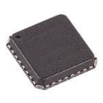
| 产品图片 |
|
| rohs | RoHS 合规性豁免无铅 / 符合限制有害物质指令(RoHS)规范要求 |
| 产品系列 | 加速计,Analog Devices ADXL312ACPZ- |
| 数据手册 | |
| 产品型号 | ADXL312ACPZ |
| 产品种类 | 加速计 |
| 传感轴 | Triple |
| 供应商器件封装 | 32-LFCSP-LQ (5x5) |
| 其它名称 | ADXL312WACPZ |
| 分辨率 | 16 bit |
| 加速 | 1.5 g, 3 g, 6 g, 12 g |
| 加速度范围 | ±1.5g, 3g, 6g, 12g |
| 商标 | Analog Devices |
| 安装类型 | 表面贴装 |
| 安装风格 | SMD/SMT |
| 封装 | Tube |
| 封装/外壳 | 32-LFQFN 裸露焊盘,CSP |
| 封装/箱体 | LFCSP-32 |
| 工厂包装数量 | 60 |
| 带宽 | 6.25Hz ~ 3.2kHz 可选 |
| 接口 | SPI |
| 数字输出-总线接口 | SPI |
| 最大工作温度 | + 175 C |
| 最小工作温度 | - 40 C |
| 标准包装 | 60 |
| 灵敏度 | 345LSB/g,172LSB/g,86LSB/g,43LSB/g |
| 电压-电源 | 2 V ~ 3.6 V |
| 电源电压-最大 | 3.6 V |
| 电源电压-最小 | 2 V |
| 电源电流 | 170 uA |
| 系列 | ADXL312 |
| 视频文件 | http://www.digikey.cn/classic/video.aspx?PlayerID=1364138032001&width=640&height=505&videoID=2245193160001http://www.digikey.cn/classic/video.aspx?PlayerID=1364138032001&width=640&height=505&videoID=2245193171001http://www.digikey.cn/classic/video.aspx?PlayerID=1364138032001&width=640&height=505&videoID=2245193161001http://www.digikey.cn/classic/video.aspx?PlayerID=1364138032001&width=640&height=505&videoID=2245193172001 |
| 轴 | X,Y,Z |
| 输出类型 | Digital |


- 商务部:美国ITC正式对集成电路等产品启动337调查
- 曝三星4nm工艺存在良率问题 高通将骁龙8 Gen1或转产台积电
- 太阳诱电将投资9.5亿元在常州建新厂生产MLCC 预计2023年完工
- 英特尔发布欧洲新工厂建设计划 深化IDM 2.0 战略
- 台积电先进制程称霸业界 有大客户加持明年业绩稳了
- 达到5530亿美元!SIA预计今年全球半导体销售额将创下新高
- 英特尔拟将自动驾驶子公司Mobileye上市 估值或超500亿美元
- 三星加码芯片和SET,合并消费电子和移动部门,撤换高东真等 CEO
- 三星电子宣布重大人事变动 还合并消费电子和移动部门
- 海关总署:前11个月进口集成电路产品价值2.52万亿元 增长14.8%
PDF Datasheet 数据手册内容提取
3-Axis, ±1.5 g/±3 g/±6 g/±12 g Digital Accelerometer Data Sheet ADXL312 FEATURES GENERAL DESCRIPTION Ultralow power: as low as 57 µA in measurement mode and The ADXL3121 is a small, thin, low power, 3-axis accelerometer 0.1 µA in standby mode at VS = 3.3 V (typical) with high resolution (13-bit) measurement up to ±12 g. Digital Power consumption scales automatically with bandwidth output data is formatted as 16-bit twos complement and is User-selectable resolution accessible through either a serial port interface (SPI) (3- or 4-wire) Fixed 10-bit resolution or I2C digital interface. Full resolution, where resolution increases with g range, The ADXL312 is well suited for car alarm or black box applica- up to 13-bit resolution at ±12 g (maintaining 2.9 mg/LSB tions. It measures the static acceleration of gravity in tilt-sensing scale factor in all g ranges) applications, as well as dynamic acceleration resulting from motion Embedded FIFO technology minimizes host processor load or shock. Its high resolution (2.9 mg/LSB) enables resolution of Built-in motion detection functions for activity/inactivity inclination changes of as little as 0.25°. A built-in FIFO facili- monitoring tates using oversampling techniques to improve resolution to as Supply and I/O voltage range: 2.0 V to 3.6 V little as 0.05° of inclination. SPI (3- and 4-wire) and I2C digital interfaces Flexible interrupt modes mappable to either interrupt pin Several special sensing functions are provided. Activity and Measurement ranges selectable via serial command inactivity sensing detects the presence or absence of motion and Bandwidth selectable via serial command whether the acceleration on any axis exceeds a user-set level. Wide temperature range (−40 to +105°C) These functions can be mapped to interrupt output pins. An 10,000 g shock survival integrated 32 level FIFO can be used to store data to minimize Pb free/RoHS compliant host processor intervention. Small and thin: 5 mm × 5 mm × 1.45 mm LFCSP package Low power modes enable intelligent motion-based power Qualified for automotive applications management with threshold sensing and active acceleration APPLICATIONS measurement at extremely low power dissipation. Car alarm The ADXL312 is supplied in a small, thin 5 mm × 5 mm × Hill start aid (HSA) 1.45 mm, 32-lead, LFCSP package. Electronic parking brake Data recorder (black box) FUNCTIONAL BLOCK DIAGRAM VS VDD I/O ADXL312 POWER MANAGEMENT CONTROL INT1 SENSE ADC AND ELECTRONICS DIGITAL INTERRUPT 3-AXIS FILTER LOGIC INT2 SENSOR SDA/SDI/SDIO 32 FLIEFVOEL SERIAL I/O SDO/ALT ADDRESS SCL/SCLK GND CS 08791-001 Figure 1. ADXL312 Simplified Block Diagram 1 Protected by U.S. Patent 8,156,264B2. Rev. B Document Feedback Information furnished by Analog Devices is believed to be accurate and reliable. However, no responsibility is assumed by Analog Devices for its use, nor for any infringements of patents or other One Technology Way, P.O. Box 9106, Norwood, MA 02062-9106, U.S.A. rights of third parties that may result from its use. Specifications subject to change without notice. No license is granted by implication or otherwise under any patent or patent rights of Analog Devices. Tel: 781.329.4700 ©2010–2017 Analog Devices, Inc. All rights reserved. Trademarks and registered trademarks are the property of their respective owners. Technical Support www.analog.com
ADXL312 Data Sheet TABLE OF CONTENTS Features .............................................................................................. 1 FIFO ............................................................................................. 18 Applications ....................................................................................... 1 Self-Test ....................................................................................... 19 General Description ......................................................................... 1 Register Map ................................................................................... 20 Functional Block Diagram .............................................................. 1 Register Definitions ................................................................... 21 Revision History ............................................................................... 2 Applications Information .............................................................. 25 Specifications ..................................................................................... 3 Power Supply Decoupling ......................................................... 25 Absolute Maximum Ratings ............................................................ 5 Mechanical Considerations for Mounting .............................. 25 Thermal Resistance ...................................................................... 5 Threshold .................................................................................... 25 ESD Caution .................................................................................. 5 Link Mode ................................................................................... 25 Pin Configuration and Function Descriptions ............................. 6 Sleep Mode vs. Low Power Mode............................................. 25 Typical Performance Characteristics ............................................. 7 Using Self-Test ............................................................................ 26 Theory of Operation ...................................................................... 10 Data Formatting of Upper Data Rates ..................................... 27 Power Sequencing ...................................................................... 10 Noise Performance ..................................................................... 28 Power Savings.............................................................................. 10 Axes of Acceleration Sensitivity ............................................... 29 Serial Communications ................................................................. 12 Solder Profile ................................................................................... 30 SPI ................................................................................................. 12 Outline Dimensions ....................................................................... 31 I2C ................................................................................................. 15 Ordering Guide .......................................................................... 32 Interrupts ..................................................................................... 17 Automotive Products ................................................................. 32 REVISION HISTORY 4/2017—Rev. A to Rev. B Added Serial Port I/O Default States Section ............................. 12 Changes to Standby Mode Leakage Current Parameter, Table 1 ...... 3 Added Preventing Bus Traffic Errors Section and Figure 23; Updated Outline Dimensions ....................................................... 31 Renumbered Sequentially ............................................................. 13 Changes to Ordering Guide .......................................................... 32 Changes to FIFO Section ............................................................... 18 Changes to Figure 41 ...................................................................... 31 7/2015—Rev. 0 to Rev. A Changes to Features Section............................................................ 1 12/2010—Revision 0: Initial Version Changes to Pin 22 Description, Table 4 ......................................... 6 Changes to Serial Communications Section, SPI Section, Figure 21, and Figure 22 ................................................................ 12 Rev. B | Page 2 of 32
Data Sheet ADXL312 SPECIFICATIONS T = −40°C to +105°C, V = V = 3.3 V, acceleration = 0 g, unless otherwise noted. A S DD I/O Table 1. Specifications1 Parameter Test Conditions/Comments Min Typ Max Unit SENSOR INPUT Each axis Measurement Range User selectable ±1.5, 3, 6, 12 g Nonlinearity Percentage of full scale ±0.5 % Inter-Axis Alignment Error ±0.1 Degrees Cross-Axis Sensitivity2 ±1 % OUTPUT RESOLUTION Each axis All g Ranges Default resolution 10 Bits ±1.5 g Range Full resolution enabled 10 Bits ±3 g Range Full resolution enabled 11 Bits ±6 g Range Full resolution enabled 12 Bits ±12 g Range Full resolution enabled 13 Bits SENSITIVITY Each axis Scale Factor at X , Y , Z ±1.5 g, 10-bit or full resolution 2.6 2.9 3.2 mg/LSB OUT OUT OUT Scale Factor at X , Y , Z ±3 g, 10-bit resolution 5.2 5.8 6.4 mg/LSB OUT OUT OUT Scale Factor at X , Y , Z ±6 g, 10-bit resolution 10.4 11.6 12.8 mg/LSB OUT OUT OUT Scale Factor at X , Y , Z ±12 g, 10-bit resolution 20.9 23.2 25.5 mg/LSB OUT OUT OUT Sensitivity at X , Y , Z ±1.5 g, 10-bit or full resolution 312 345 385 LSB/g OUT OUT OUT Sensitivity at X , Y , Z ±3 g, 10-bit resolution 156 172 192 LSB/g OUT OUT OUT Sensitivity at X , Y , Z ±6 g, 10-bit resolution 78 86 96 LSB/g OUT OUT OUT Sensitivity at X , Y , Z ±12 g, 10-bit resolution 39 43 48 LSB/g OUT OUT OUT Sensitivity Change Due to Temperature ±0.01 %/°C 0 g BIAS LEVEL Each axis Initial 0 g Output T = 25°C, X , Y −150 +150 mg OUT OUT Initial 0 g Output T = 25°C, Z −250 +250 mg OUT 0 g Output over Temperature −40°C < T < 105°C, X , Y , Z −250 +250 mg OUT OUT OUT 0 g Offset Tempco X , Y ±0.8 mg/°C OUT OUT 0 g Offset Tempco Z ±1.5 mg/°C OUT NOISE PERFORMANCE Noise Density (X-, Y-axes) 200 340 440 µg/√Hz Noise Density (Z-axis) 200 470 595 µg/√Hz OUTPUT DATA RATE/BANDWIDTH User selectable Measurement Rate3 6.25 3200 Hz SELF-TEST4 Data rate ≥ 100 Hz, 2.0 ≤ VS ≤ 3.6 Output Change in X-Axis 0.20 2.10 g Output Change in Y-Axis −2.10 −0.20 g Output Change in Z-Axis 0.30 3.40 g Rev. B | Page 3 of 32
ADXL312 Data Sheet Parameter Test Conditions/Comments Min Typ Max Unit POWER SUPPLY Operating Voltage Range (V) 2.0 3.6 V S Interface Voltage Range (V ) 1.7 V V DD I/O S Supply Current Data rate > 100 Hz 100 170 300 µA Data rate < 10 Hz 30 55 110 µA Standby Mode Leakage Current T = 25°C 0.1 2 µA Over entire operating temperature range 17 µA Turn-On (Wake-Up) Time5 1.4 ms TEMPERATURE Operating Temperature Range −40 +105 °C 1 All minimum and maximum specifications are guaranteed. Typical specifications are not guaranteed. 2 Cross-axis sensitivity is defined as coupling between any two axes. 3 Bandwidth is half the output data rate. 4 Self-test change is defined as the output (g) when the SELF_TEST bit = 1 (in the DATA_FORMAT register) minus the output (g) when the SELF_TEST bit = 0 (in the DATA_FORMAT register). Due to device filtering, the output reaches its final value after 4 × τ when enabling or disabling self-test, where τ = 1/(data rate). 5 Turn-on and wake-up times are determined by the user-defined bandwidth. At a 100 Hz data rate, the turn-on and wake-up times are each approximately 11.1 ms. For other data rates, the turn-on and wake-up times are each approximately τ + 1.1 in milliseconds, where τ = 1/(data rate). Rev. B | Page 4 of 32
Data Sheet ADXL312 ABSOLUTE MAXIMUM RATINGS Table 2. THERMAL RESISTANCE Parameter Rating θ is specified for the worst-case conditions, that is, a device JA Acceleration soldered in a circuit board for surface-mount packages. Any Axis, Unpowered 10,000 g Any Axis, Powered 10,000 g Table 3. Thermal Resistance VS −0.3 V to 3.9 V Package Type θJA θJC Unit V −0.3 V to 3.9 V 32-Lead LFCSP Package 27.27 30 °C/W DD I/O All Other Pins −0.3 V to V + 0.3 V or DD I/O 3.9 V, whichever is less ESD CAUTION Output Short-Circuit Duration Indefinite (Any Pin to Ground) Temperature Range Powered −40°C to +125°C Storage −40°C to +125°C Stresses at or above those listed under Absolute Maximum Ratings may cause permanent damage to the product. This is a stress rating only; functional operation of the product at these or any other conditions above those indicated in the operational section of this specification is not implied. Operation beyond the maximum operating conditions for extended periods may affect product reliability. Rev. B | Page 5 of 32
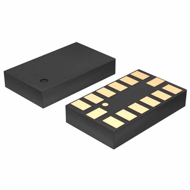
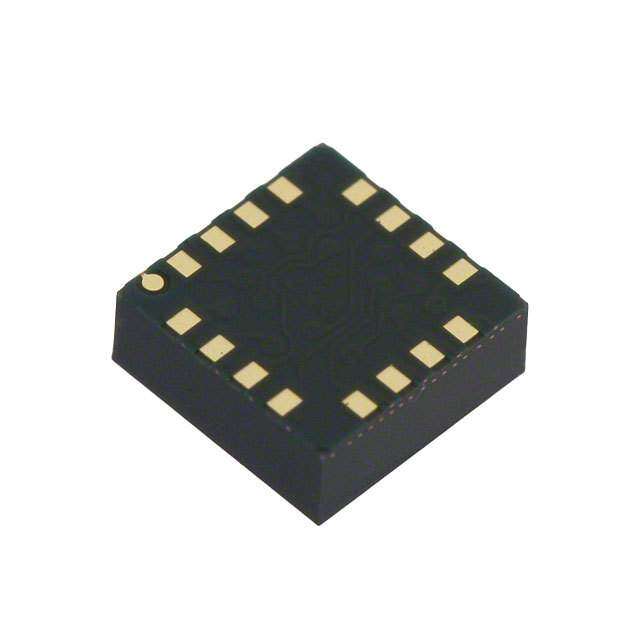
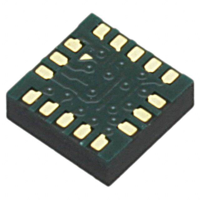
ADXL312 Data Sheet PIN CONFIGURATION AND FUNCTION DESCRIPTIONS K L C DD I/OCCCCCL/SCC NVNNNNSN 21098765 33322222 GND 1 24 SDA/SDI/SDIO RESERVED 2 23 SPO/ALTADDRESS GND 3 22 RESERVED ADXL312 GND 4 21 INT2 TOP VIEW VS 5 (Not to Scale) 20 INT1 CS 6 19 NC RESERVED 7 18 NC NC 8 17 NC 910111213141516 CCCCCCCC NNNNNNNN N12..O TNTHCEE S= E NXOP OCOSENDNEPCATD. MDOUS NTO BTE C SOONLNDEECRTETDOT TOH TISH EP IGNR.OUND PLANE. 08791-002 Figure 2. Pin Configuration (Top View) Table 4. Pin Function Descriptions Pin No. Mnemonic Description 1 GND This pin must be connected to ground. 2 Reserved Reserved. This pin must be connected to V or left open. S 3 GND This pin must be connected to ground. 4 GND This pin must be connected to ground. 5 V Supply Voltage. S 6 CS Chip Select. 7 Reserved Reserved. This pin must be left open. 8 to19 NC No Connect. Do not connect to this pin. 20 INT1 Interrupt 1 Output. 21 INT2 Interrupt 2 Output. 22 Reserved Reserved. This pin must be connected to GND. 23 SDO/ALT ADDRESS Serial Data Out, Alternate I2C Address Select. 24 SDA/SDI/SDIO Serial Data (I2C), Serial Data In (SPI 4-Wire), Serial Data In/Out (SPI 3-Wire). 25 NC No Connect. Do not connect to this pin. 26 SCL/SCLK Serial Communications Clock. 27 to 30 NC No Connect. Do not connect to this pin. 31 V Digital Interface Supply Voltage. DD I/O 32 NC No Connect. EP The exposed pad must be soldered to the ground plane. Rev. B | Page 6 of 32
Data Sheet ADXL312 TYPICAL PERFORMANCE CHARACTERISTICS N > 1000, unless otherwise noted. 40 40 35 35 %) %) N ( 30 N ( 30 O O TI TI A 25 A 25 L L U U P P PO 20 PO 20 F F O O T 15 T 15 N N E E C C R 10 R 10 E E P P 5 5 0–150 –120 –90 –60ZE–R3O0g OF0FSET3 0(mg)60 90 120 150 08791-003 0 –3.0 –2.5ZER–2.0Og –1.5TEMP–1.0ERA–0.5TURE0 COE0.5FFIC1.0IENT1.5 (mg2.0/°C) 2.5 3.0 08791-006 Figure 3. X-Axis Zero-g Bias. 25°C, VS = VDD I/O = 3.3 V Figure 6. X-Axis Zero-g Bias Drift, VS = VDD I/O = 3.3 V 35 40 30 35 %) %) ON ( 25 ON ( 30 TI TI A A 25 L L U 20 U P P PO PO 20 OF 15 OF T T 15 N N E E C 10 C ER ER 10 P P 5 5 0–150 –120 –90 –60ZE–R3O0g OF0FSET3 0(mg)60 90 120 150 08791-004 0 –3.0 –2.5ZER–2.0Og –1.5TEMP–1.0ERA–0.5TURE0 COE0.5FFIC1.0IENT1.5 (mg2.0/°C) 2.5 3.0 08791-007 Figure 4. Y Axis Zero-g Bias, 25°C, VS = VDD I/O = 3.3 V Figure 7. Y-Axis Zero-g Bias Drift, VS = VDD I/O = 3.3 V 50 25 45 %) 40 %) 20 N ( N ( O 35 O TI TI A A L 30 L 15 U U P P PO 25 PO F F T O 20 T O 10 N N CE 15 CE R R E E P 10 P 5 5 0–250 –200 –150 –100ZE–R5O0g OF0FSET5 0(mg)100 150 200 250 08791-005 0 –3.0 –2.5ZER–2.0Og –1.5TEMP–1.0ERA–0.5TURE0 COE0.5FFIC1.0IENT1.5 (mg2.0/°C) 2.5 3.0 08791-008 Figure 5. Z Axis Zero-g Bias, 25°C, VS = VDD I/O = 3.3 V Figure 8. Z-Axis Zero-g Bias Drift, VS = VDD I/O = 3.3 V Rev. B | Page 7 of 32
ADXL312 Data Sheet 70 30 60 25 %) %) ON ( 50 ON ( TI TI 20 A A L L U 40 U P P PO PO 15 OF 30 OF T T EN EN 10 C 20 C R R E E P P 5 10 0 0 2 8 4 0 6 2 8 4 0 6 2 8 4 0 5 0 5 0 5 0 5 0 5 0 5 0 31 31 32 33 33SENS34ITIVI34TY (L35SB/g36) 36 37 37 38 08791-009 –0.03 –0.02SENS–0.02ITIVI–0.01TY TE–0.01MPE–0.00RATURE 0.00COEF0.01FICIE0.01NT (0.02%/°C0.02) 0.03 08791-012 Figure 9. X-Axis Sensitivity, VS = VDD I/O = 3.3 V, 25°C Figure 12. X-Axis Sensitivity Temperature Coefficient, VS = VDD I/O = 3.3 V 70 35 60 30 %) %) ON ( 50 ON ( 25 OPULATI 40 OPULATI 20 OF P 30 OF P 15 NT NT RCE 20 RCE 10 PE PE 10 5 0 0 312 318 324 330 336SENS342ITIVI348TY (L354SB/g360) 366 372 378 384 08791-010 –0.030 –0.025SENS–0.020ITIVI–0.015TY TE–0.010MPE–0.005RATU0RE C0.005OEF0.010FICIE0.015NT 0.020(%/°C0.025) 0.030 08791-013 Figure 10. Y-Axis Sensitivity, VS = VDD I/O = 3.3 V, 25°C Figure 13. Y-Axis Sensitivity Temperature Coefficient, VS = VDD I/O = 3.3 V 70 35 60 30 %) %) ON ( 50 ON ( 25 ATI ATI L L U 40 U 20 P P O O P P OF 30 OF 15 T T N N E E C 20 C 10 R R E E P P 10 5 0 0 2 8 4 0 6 2 8 4 0 6 2 8 4 0 5 0 5 0 5 0 5 0 5 0 5 0 31 31 32 33 33SENS34ITIVI34TY (L35SB/g36) 36 37 37 38 08791-011 –0.03 –0.02SENS–0.02ITIVI–0.01TY TE–0.01MPE–0.00RATURE C0.00OEF0.01FICIE0.01NT (0.02%/°C0.02) 0.03 08791-014 Figure 11. Z-Axis Sensitivity, VS = VDD I/O = 3.3 V, 25°C Figure 14. Z-Axis Sensitivity Temperature Coefficient, VS = VDD I/O = 3.3 V Rev. B | Page 8 of 32
Data Sheet ADXL312 80 80 70 70 %) %) N ( 60 N ( 60 O O ATI 50 ATI 50 L L U U P P PO 40 PO 40 F F O O T 30 T 30 N N E E C C ER 20 ER 20 P P 10 10 0 0.2 0.4 0.6 S0E.8LF-T1E.S0T R1E.S2PON1.S4E (g1).6 1.8 2.0 08791-015 0 30 50 70 90 110 130CU150RRE170NT (190nA)210 230 250 270 290 310 08791-018 Figure 15. X-Axis Self-Test Delta, VS = VDD I/O = 3.3 V, 25°C Figure 18. Standby Mode Current Consumption, VS = VDD I/O = 3.3 V, 25°C 70 35 60 30 %) %) ON ( 50 ON ( 25 TI TI A A L L U 40 U 20 P P O O P P OF 30 OF 15 T T N N E E C 20 C 10 R R E E P P 10 5 0 –2.1 –1.9 –1.7 SE–1.5LF-TE–1.3ST RE–1.1SPON–0.9SE (g)–0.7 –0.5 –0.3 08791-016 0 100 120 140CUR160RENT180 CON200SUMP220TION (240µA) 260 280 300 08791-019 Figure 16. Y-Axis Self-Test Delta, VS = VDD I/O = 3.3 V, 25°C Figure 19. Current Consumption, Measurement Mode, Data Rate = 100 Hz, VS = VDD I/O = 3.3 V, 25°C 80 200 70 %) ON ( 60 A)150 ATI 50 T (µ L N U E P R PO 40 UR100 OF Y C ERCENT 3200 SUPPL 50 P 10 0 0.3 0.6 0.9 1S.2ELF1-.T5EST1 .R8ES2P.O1NS2E.4 (g)2.7 3.0 3.3 08791-017 02.0 2.4 SUPPLY V2O.8LTAGE (V) 3.2 3.6 08791-233 Figure 17. Z-Axis Self-Test Delta, VS = VDD I/O = 3.3 V, 25°C Figure 20. Supply Current vs. Supply Voltage, VS at 25°C Rev. B | Page 9 of 32
ADXL312 Data Sheet THEORY OF OPERATION The ADXL312 is a complete 3-axis acceleration measurement Table 5. Power Sequencing system with a selectable measurement range of ±1.5 g, ±3 g, Condition V V Description S DD I/O ±6 g, or ±12 g. It measures both dynamic acceleration resulting Power Off Off Off The device is completely off, but from motion or shock and static acceleration, such as gravity, there is a potential for a which allows it to be used as a tilt sensor. communication bus conflict. Bus Disabled On Off The device is on in standby mode, The sensor is a polysilicon surface-micromachined structure but communication is unavailable built on top of a silicon wafer. Polysilicon springs suspend the and creates a conflict on the structure over the surface of the wafer and provide a resistance communication bus. The duration against acceleration forces. of this state must be minimized during power-up to prevent a Deflection of the structure is measured using differential conflict. capacitors that consist of independent fixed plates and plates Bus Enabled Off On No functions are available, but attached to the moving mass. Acceleration deflects the beam the device will not create a conflict and unbalances the differential capacitor, resulting in a sensor on the communication bus. output whose amplitude is proportional to acceleration. Phase- Standby or On On The device is in standby mode, sensitive demodulation is used to determine the magnitude and Measurement awaiting a command to enter polarity of the acceleration. measurement mode, and all sensor functions are off. After the device is POWER SEQUENCING instructed to enter measurement mode, all sensor functions are Power can be applied to V or V in any sequence without S DD I/O available. damaging the ADXL312. All possible power-on modes are POWER SAVINGS summarized in Table 5. The interface voltage level is set with the interface supply voltage, V , which must be present to Power Modes DD I/O ensure that the ADXL312 does not create a conflict on the The ADXL312 automatically modulates its power consumption communication bus. For single-supply operation, V can be DD I/O in proportion to its output data rate, as outlined in Table 6. If the same as the main supply, V. In a dual-supply application, S additional power savings is desired, a lower power mode is however, V can differ from V to accommodate the desired DD I/O S available. In this mode, the internal sampling rate is reduced, interface voltage, as long as V is greater than or equal to V . S DD I/O allowing for power savings in the 12.5 Hz to 400 Hz data rate After VS is applied, the device enters standby mode, where power range at the expense of slightly greater noise. To enter low consumption is minimized and the device waits for VDD I/O to be power mode, set the LOW_POWER bit (Bit 4) in the BW_RATE applied and for the command to enter measurement mode to be register (Address 0x2C). The current consumption in low power received. (This command can be initiated by setting the measure mode is shown in Table 7 for cases where there is an advantage bit in the POWER_CTL register (Address 0x2D).) In addition, any to using low power mode. Use of low power mode for a data register can be written to or read from to configure the part while rate not shown in Table 7 does not provide any advantage over the device is in standby mode. It is recommended to configure the the same data rate in normal power mode. Therefore, it is device in standby mode and then to enable measurement mode. recommended that only data rates shown in Table 7 be used in Clearing the measure bit returns the device to the standby mode. low power mode. The current consumption values shown in Table 6 and Table 7 are for a V of 3.3 V. S Rev. B | Page 10 of 32
Data Sheet ADXL312 Table 6. Current Consumption vs. Data Rate Autosleep Mode (TA = 25°C, VS = VDD I/O = 3.3 V) Additional power savings can be had by having the ADXL312 Output Data automatically switch to sleep mode during periods of inactivity. Rate (Hz) Bandwidth (Hz) Rate Code I (µA) DD To enable this feature, set the THRESH_INACT register 3200 1600 1111 170 (Address 0x25) to an acceleration threshold value. Levels of 1600 800 1110 115 acceleration below this threshold are regarded as no activity 800 400 1101 170 levels. Set TIME_INACT (Address 0x26) to an appropriate 400 200 1100 170 inactivity time period. Then set the AUTO_SLEEP bit and the 200 100 1011 170 link bit in the POWER_CTL register (Address 0x2D). If the 100 50 1010 170 device does not detect a level of acceleration in excess of 50 25 1001 115 THRES_INACT for TIME_INACT seconds, then the device is 25 12.5 1000 82 transitioned to sleep mode automatically. Current consumption 12.5 6.25 0111 65 at the sub-8 Hz data rates used in this mode is typically 30 µA 6.25 3.125 0110 57 for a V of 3.3 V. S Standby Mode Table 7. Current Draw vs. Data Rate, Low Power Mode (TA = 25°C, VS = VDD I/O = 3.3 V) For even lower power operation, standby mode can be used. In Output Data standby mode, current consumption is reduced to 0.1µA Rate (Hz) Bandwidth (Hz) Rate Code IDD (µA) (typical). In this mode, no measurements are made. Standby 400 200 1100 115 mode is entered by clearing the measure bit (Bit 3) in the 200 100 1011 82 POWER_CTL register (Address 0x2D). Placing the device into 100 50 1010 65 standby mode preserves the contents of the FIFO. 50 25 1001 57 25 12.5 1000 50 12.5 6.25 0111 43 Rev. B | Page 11 of 32
ADXL312 Data Sheet SERIAL COMMUNICATIONS The ADXL312 can communicate via I2C and SPI digital When using 3-wire SPI, pull the SDO pin up to V or down DD I/O communications interfaces. In both cases, the ADXL312 operates to ground via a 10 kΩ resistor, as shown in Figure 21. as a slave. If I2C is the desired interface for the application, tie CS is the serial port enable line and is controlled by the SPI master. the CS pin directly to V as shown in Figure 27. If SPI is the DD I/O This line must go low at the start of a transmission and high at desired interface for the application, drive the CS pin with an the end of a transmission, as shown in Figure 24. SCLK is the external controller, as demonstrated in Figure 21 and Figure 22. serial port clock and is supplied by the SPI master. SDI and Because the I2C interface is enabled any time the CS pin is brought SDO are the serial data input and output, respectively. up to V , there is a potential for bus conflicts to occur when the DD I/O ADXL312 PROCESSOR ADXL312 is implemented into a SPI network. Refer to the CS D_OUT Preventing Bus Traffic Errors section for information on how to SDIO D_IN/OUT avoid such conditions. In both SPI and I2C modes of operation, SDO idgunroinreg dwartait etrsa tnos mthiett eAdD fXroLm3 1th2e. ADXL312 to the master device SCLK RPD D_OUT 08791-044 Note that throughout this section, multifunction pins, such as SDA/SDI/SDIO, are referred to either by the entire pin name or Figure 21. 3-Wire SPI Connection Diagram by a single function of the pin, for example, SDA, when only ADXL312 PROCESSOR that function is relevant. CS D_OUT SERIAL PORT I/O DEFAULT STATES SDI D_OUT SDO D_IN Epinns uisr ea ltlhoawte adl lt soe frlioaal tp worhte In/O nso ta rine iuns ea. dTehfiins eisd a sptaptleic aanbdle tthoa at lnl o SCLK D_OUT 08791-045 serial port I/Os, regardless of SPI or I2C operation. Figure 22. 4-Wire SPI Connection Diagram For I2C applications, always tie the CS pin high to VDD I/O. To read or write multiple bytes in a single transmission, the Connect the SCL and SDA pins to an external controller, with multiple-byte bit, located after the R/W bit in the first byte transfer pull-up resistors implemented according to the UM10204 I2C- (MB in Figure 24 to Figure 26), must be set. After the register Bus Specification and User Manual, Rev. 03—19 June 2007, addressing and the first byte of data, each subsequent set of available from NXP Semiconductor. The ALT ADDRESS pin clock pulses (eight clock pulses) causes the ADXL312 to point must be tied to either VDD I/O or ground, thereby selecting the to the next register for a read or write. This shifting continues desired I2C address for the ADXL312. until the clock pulses cease and CS is deasserted. To perform reads If SPI is the intended communications interface, drive the CS or writes on different nonsequential registers, CS must be pin with an external controller, as shown in Figure 21 and deasserted between transmissions, and the new register must be Figure 22. When communications with the ADXL312 are addressed separately. suspended (CS = VDD I/O), ensure that the SCLK, SDI/SDIO, and The timing diagram for 3-wire SPI reads or writes is shown in SDO pins are not floating. Figure 26. The 4-wire equivalents for SPI writes and reads are For either SPI or I2C operation, not taking these precautions may shown in Figure 24 and Figure 25, respectively. For correct opera- result in an inability to communicate with the device or excessive tion of the device, the logic thresholds and timing parameters in current consumption. Table 8 and Table 9 must be met at all times. SPI Use of the 3200 Hz and 1600 Hz output data rates is only recommended with SPI communication rates greater than or For the SPI, either 3- or 4-wire configuration is possible, as shown equal to 2 MHz. The 800 Hz output data rate is recommended in the connection diagrams in Figure 21 and Figure 22. Clearing only for communication speeds greater than or equal to 400 kHz, the SPI bit in the DATA_FORMAT register (Address 0x31) and the remaining data rates scale proportionally. For example, selects 4-wire mode, whereas setting the SPI bit selects 3-wire the minimum recommended communication speed for a 200 Hz mode. The maximum SPI clock speed is 5 MHz with 100 pF output data rate is 100 kHz. Operation at an output data rate maximum loading, and the timing scheme follows clock polarity below the recommended minimum may result in undesirable (CPOL) = 1 and clock phase (CPHA) = 1. If power is applied to effects on the acceleration data, including missing samples or the ADXL312 before the clock polarity and phase of the host additional noise. processor are configured, bring the CS pin high before changing the clock polarity and phase. Rev. B | Page 12 of 32
Data Sheet ADXL312 Preventing Bus Traffic Errors This OR gate holds the SDA line high when CS is high to The ADXL312 CS pin initiates SPI transactions and enables I2C prevent bus traffic at the ADXL312 from appearing as an I2C start command. mode. When the ADXL312 is used on a SPI bus with multiple devices, its CS pin is held high while the master communicates ADXL312 PROCESSOR with the other devices. There may be conditions where a SPI CS D_OUT command transmitted to another device looks like a valid I2C SDI D_OUT command. In this case, the ADXL312 interprets this as an oatttheemr pbtu tso t rcaofmficm. Uunnilceastse b iuns I t2Cra fmfico dcaen a nbde amdaeyq uinatteerlyfe creo nwtirtohl led SSCDLOK DD__IONUT 08791-046 Figure 23. Recommended SPI Connection Diagram when Using Multiple SPI to ensure such a condition never occurs, it is recommended to Devices on a Single Bus add a logic gate in front of the SDI pin, as shown in Figure 23. Table 8. SPI Digital Input/Output Limit1 Parameter Test Conditions Min Max Unit Digital Input Low Level Input Voltage (V ) 0.3 × V V IL DD I/O High Level Input Voltage (V ) 0.7 × V V IH DD I/O Low Level Input Current (I ) V = V 0.1 µA IL IN DD I/O High Level Input Current (I ) V = 0 V −0.1 µA IH IN Digital Output Low Level Output Voltage (V ) I = 10 mA 0.2 × V V OL OL DD I/O High Level Output Voltage (V ) I = −4 mA 0.8 × V V OH OH DD I/O Low Level Output Current (I ) V = V 10 mA OL OL OL, max High Level Output Current (I ) V = V −4 mA OH OH OH, min Pin Capacitance f = 1 MHz, V = 2.5 V 8 pF IN IN 1 Limits based on characterization results, not production tested. Table 9. SPI Timing (T = 25°C, V = V = 3.3 V)1 A S DD I/O Limit2, 3 Parameter Min Max Unit Description f 5 MHz SPI clock frequency. SCLK t 200 ns 1/(SPI clock frequency) mark-space ratio for the SCLK input is 40/60 to 60/40. SCLK tDELAY 5 ns CS falling edge to SCLK falling edge . tQUIET 5 ns SCLK rising edge to CS rising edge. tDIS 10 ns CS rising edge to SDO disabled. tCS,DIS 150 ns CS deassertion between SPI communications. t 0.3 × t ns SCLK low pulse width (space). S SCLK t 0.3 × t ns SCLK high pulse width (mark). M SCLK t 5 ns SDI valid before SCLK rising edge. SETUP t 5 ns SDI valid after SCLK rising edge. HOLD t 40 ns SCLK falling edge to SDO/SDIO output transition. SDO t4 20 ns SDO/SDIO output high to output low transition. R t4 20 ns SDO/SDIO output low to output high transition. F 1 The CS, SCLK, SDI, and SDO pins are not internally pulled up or down; they must be driven for proper operation. 2 Limits based on characterization results, characterized with fSCLK = 5 MHz and bus load capacitance of 100 pF; not production tested. 3 The timing values are measured corresponding to the input thresholds (VIL and VIH) given in Table 8. 4 Output rise and fall times measured with capacitive load of 150 pF. Rev. B | Page 13 of 32
ADXL312 Data Sheet CS tDELAY tSCLK tM tS tQUIET tCS,DIS SCLK tSETUP tHOLD SDI W MB A5 A0 D7 D0 tSDO ADDRESS BITS DATA BITS tDIS SDO X X X tR,tXF X X 08791-129 Figure 24. SPI 4-Wire Write CS tDELAY tSCLK tM tS tQUIET tCS,DIS SCLK tSETUP tHOLD SDI R MB A5 A0 X X tSDO ADDRESS BITS tDIS SDO X X X X D7 D0 tR,tF DATA BITS 08791-130 Figure 25. SPI 4-Wire Read CS tDELAY tSCLK tM tS tQUIET tCS,DIS SCLK tSETUP tHOLD tR,tF tSDO SDIO R/W MB A5 A0 D7 D0 ADDRESS BITS DATA BITS SDO N1.OtTSDEOS IS ONLY PRESENT DURING READS. 08791-131 Figure 26. SPI 3-Wire Read/Write Rev. B | Page 14 of 32
Data Sheet ADXL312 I2C VDD I/O With CS tied high to V , the ADXL312 is in I2C mode, DD I/O ADXL312 RP RP PROCESSOR requiring a simple 2-wire connection as shown in Figure 27. The ADXL312 conforms to the UM10204 I2C-Bus Specification CS SDA D IN/OUT and User Manual, Rev. 03—19 June 2007, available from NXP ALT ADDRESS Semiconductor. It supports standard (100 kHz) and fast (400 kHz) dTaatbal et r1a1n asfreer m meot.d Seisn igf lteh-e o br ums uplatirpalme-ebtyetres rgeivadens/ iwnr Titaebs laer 1e 0 and SCL D OUT 08791-032 Figure 27. I2C Connection Diagram (Address 0x53) supported, as shown in Figure 28. With the ALT ADDRESS pin high, the 7-bit I2C address for the device is 0x1D, followed by the If other devices are connected to the same I2C bus, the nominal R/W bit. This translates to 0x3A for a write and 0x3B for a read. An operating voltage level of these other devices cannot exceed VDD I/O alternate I2C address of 0x53 (followed by the R/W bit) can be by more than 0.3 V. External pull-up resistors, RP, are necessary chosen by grounding the ALT ADDRESS pin (Pin 7). This for proper I2C operation. Refer to the UM10204 I2C-Bus translates to 0xA6 for a write and 0xA7 for a read. Specification and User Manual, Rev. 03—19 June 2007, when selecting pull-up resistor values to ensure proper operation. Table 10. I2C Digital Input/Output Limit1 Parameter Test Conditions Min Max Unit Digital Input Low Level Input Voltage (V ) 0.3 × V V IL DD I/O High Level Input Voltage (V ) 0.7 × V V IH DD I/O Low Level Input Current (I ) V = V 0.1 µA IL IN DD I/O High Level Input Current (I ) V = 0 V −0.1 µA IH IN Digital Output Low Level Output Voltage (V ) V < 2 V, I = 3 mA 0.2 × V V OL DD I/O OL DD I/O V ≥ 2 V, I = 3 mA 400 mV DD I/O OL Low Level Output Current (I ) V = V 3 mA OL OL OL, max Pin Capacitance f = 1 MHz, V = 2.5 V 8 pF IN IN 1 Limits based on characterization results; not production tested. SINGLE-BYTE WRITE MASTER START SLAVE ADDRESS + WRITE REGISTER ADDRESS DATA STOP SLAVE ACK ACK ACK MULTIPLE-BYTE WRITE MASTER START SLAVE ADDRESS + WRITE REGISTER ADDRESS DATA DATA STOP SLAVE ACK ACK ACK ACK SINGLE-BYTE READ MASTER START SLAVE ADDRESS + WRITE REGISTER ADDRESS START1 SLAVE ADDRESS + READ NACK STOP SLAVE ACK ACK ACK DATA MULTIPLE-BYTE READ MASTER START SLAVE ADDRESS + WRITE REGISTER ADDRESS START1 SLAVE ADDRESS + READ ACK NACK STOP SLAVE ACK ACK ACK DATA DATA N12..O TTTHHEEISS S SHTAADRETD I SA REIETAHSE RR EAP RREESSTEANRTT W OHRE NA TSHTOE PD EFVOILCLEO IWS ELDIS TBEYN AIN SGT.ART. 08791-033 Figure 28. I2C Device Addressing Rev. B | Page 15 of 32
ADXL312 Data Sheet Table 11. I2C Timing (T = 25°C, V = V = 3.3 V) A S DD I/O Limit1, 2 Parameter Min Max Unit Description f 400 kHz SCL clock frequency SCL t 2.5 µs SCL cycle time 1 t 0.6 µs t , SCL high time 2 HIGH t 1.3 µs t , SCL low time 3 LOW t 0.6 µs t , start/repeated start condition hold time 4 HD, STA t 100 ns t , data setup time 5 SU, DAT t3, 4, 5, 6 0 0.9 µs t , data hold time 6 HD, DAT t 0.6 µs t , setup time for repeated start 7 SU, STA t 0.6 µs t , stop condition setup time 8 SU, STO t 1.3 µs t , bus-free time between a stop condition and a start condition 9 BUF t 300 ns t , rise time of both SCL and SDA when receiving 10 R 0 ns t , rise time of both SCL and SDA when receiving or transmitting R t 250 ns t, fall time of SDA when receiving 11 F 300 ns t, fall time of both SCL and SDA when transmitting F 20 + 0.1 C 7 ns t, fall time of both SCL and SDA when transmitting or receiving b F C 400 pF Capacitive load for each bus line b 1 Limits based on characterization results, with fSCL = 400 kHz and a 3 mA sink current; not production tested. 2 All values referred to the VIH and the VIL levels given in Table 10. 3 t6 is the data hold time that is measured from the falling edge of SCL. It applies to data in transmission and acknowledge. 4 A transmitting device must internally provide an output hold time of at least 300 ns for the SDA signal (with respect to VIH(min) of the SCL signal) to bridge the undefined region of the falling edge of SCL. 5 The maximum t6 value must be met only if the device does not stretch the low period (t3) of the SCL signal. 6 The maximum value for t6 is a function of the clock low time (t3), the clock rise time (t10), and the minimum data setup time (t5(min)). This value is calculated as t6(max) = t3 − t10 − t5(min). 7 Cb is the total capacitance of one bus line in picofarads. SDA t9 t3 t10 t11 t4 SCL t4 t6 t2 t5 t7 t1 t8 COSNTDAIRTTION CROESPNTEDAAIRTTTIEODN COSNTDOITPION 08791-034 Figure 29. I2C Timing Diagram Rev. B | Page 16 of 32
Data Sheet ADXL312 DATA_READY INTERRUPTS The DATA_READY bit is set when new data is available and is The ADXL312 provides two output pins for driving interrupts: cleared when no new data is available. INT1 and INT2. Both interrupt pins are push-pull, low impedance pins with output specifications shown in Table 12. The default Activity configuration of the interrupt pins is active high. This can be The activity bit is set when acceleration greater than the value stored changed to active low by setting the INT_INVERT bit in the in the THRESH_ACT register (Address 0x24) is experienced. DATA_FORMAT (Address 0x31) register. All functions can be Inactivity used simultaneously, with the only limiting feature being that some functions may need to share interrupt pins. The inactivity bit is set when acceleration of less than the value stored in the THRESH_INACT register (Address 0x25) is Interrupts are enabled by setting the appropriate bit in the experienced for more time than is specified in the TIME_INACT INT_ENABLE register (Address 0x2E) and are mapped to either register (Address 0x26). The maximum value for TIME_INACT is the INT1 or INT2 pin based on the contents of the INT_MAP 255 sec. register (Address 0x2F). When initially configuring the interrupt Watermark pins, it is recommended that the functions and interrupt mapping be done before enabling the interrupts. When changing the con- The watermark bit is set when the number of samples in FIFO figuration of an interrupt, it is recommended that the interrupt be equals the value stored in the samples bits (Register FIFO_CTL, disabled first, by clearing the bit corresponding to that function in Address 0x38). The watermark bit is cleared automatically when the INT_ENABLE register, and then the function be reconfigured FIFO is read, and the content returns to a value below the value before enabling the interrupt again. Configuration of the functions stored in the samples bits. while the interrupts are disabled helps to prevent the accidental Overrun generation of an interrupt before desired. The overrun bit is set when new data replaces unread data. The The interrupt functions are latched and cleared by either reading precise operation of the overrun function depends on the FIFO the data registers (Address 0x32 to Address 0x37) until the inter- mode. In bypass mode, the overrun bit is set when new data rupt condition is no longer valid for the data-related interrupts replaces unread data in the DATAX, DATAY, and DATAZ registers or by reading the INT_SOURCE register (Address 0x30) for the (Address 0x32 to Address 0x37). In all other modes, the overrun remaining interrupts. This section describes the interrupts that bit is set when FIFO is filled. The overrun bit is automatically can be set in the INT_ENABLE register and monitored in the cleared when the contents of FIFO are read. INT_SOURCE register. Table 12. Interrupt Pin Digital Output Limit1 Parameter Test Conditions Min Max Unit Digital Output Low Level Output Voltage (V ) I = 300 µA 0.2 × V V OL OL DD I/O High Level Output Voltage (V ) I = −150 µA 0.8 × V V OH OH DD I/O Low Level Output Current (I ) V = V 300 µA OL OL OL, max High Level Output Current (I ) V = V −150 µA OH OH OH, min Pin Capacitance f = 1 MHz, V = 2.5 V 8 pF IN IN Rise/Fall Time Rise Time (t )2 C = 150 pF 210 ns R LOAD Fall Time (t)3 C = 150 pF 150 ns F LOAD 1 Limits based on characterization results, not production tested. 2 Rise time is measured as the transition time from VOL, max to VOH, min of the interrupt pin. 3 Fall time is measured as the transition time from VOH, min to VOL, max of the interrupt pin. Rev. B | Page 17 of 32
ADXL312 Data Sheet FIFO FIFO keeps the last n samples (where n is the value specified by the samples bits in the FIFO_CTL register) and then operates in The ADXL312 contains technology for an embedded memory FIFO mode, collecting new samples only when FIFO is not full. management system with 32-level FIFO that can be used to A delay of at least 5 μs must be present between the trigger event minimize host processor burden. This buffer has four modes: occurring and the start of reading data from the FIFO to allow bypass, FIFO, stream, and trigger (see Table 21). Each mode is the FIFO to discard and retain the necessary samples. Additional selected by the settings of the FIFO_MODE bits in the trigger events cannot be recognized until the trigger mode is FIFO_CTL register (Address 0x38). reset. To reset the trigger mode, set the device to bypass mode Bypass Mode and then set the device back to trigger mode. Note that the FIFO In bypass mode, FIFO is not operational and, therefore, data must be read first because placing the device into bypass remains empty. mode clears FIFO. FIFO Mode Retrieving Data from FIFO In FIFO mode, data from measurements of the x-, y-, and z-axes The FIFO data is read through the DATAX, DATAY, and DATAZ are stored in FIFO. When the number of samples in FIFO registers (Address 0x32 to Address 0x37). When the FIFO is in equals the level specified in the samples bits of the FIFO_CTL FIFO, stream, or trigger mode, reads to the DATAX, DATAY, register (Address 0x38), the watermark interrupt is set. FIFO and DATAZ registers read data stored in the FIFO. Each time continues accumulating samples until it is full (32 samples from data is read from the FIFO, the oldest x-, y-, and z-axes data is measurements of the x-, y-, and z-axes) and then stops collecting placed into the DATAX, DATAY and DATAZ registers. data. After FIFO stops collecting data, the device continues to If a single-byte read operation is performed, the remaining operate; therefore, features such as activity detection can be bytes of data for the current FIFO sample are lost. Therefore, all used after FIFO is full. The watermark interrupt continues to axes of interest must be read in a burst (or multiple-byte) read occur until the number of samples in FIFO is less than the value operation. To ensure that the FIFO has completely popped (that stored in the samples bits of the FIFO_CTL register. is, that new data has completely moved into the DATAX, DATAY, Stream Mode and DATAZ registers), there must be at least 5 μs between the end of reading the data registers and the start of a new read of In stream mode, data from measurements of the x-, y-, and z- the FIFO or a read of the FIFO_STATUS register (Address 0x39). axes are stored in FIFO. When the number of samples in FIFO The end of reading a data register is signified by the transition equals the level specified in the samples bits of the FIFO_CTL from Register 0x37 to Register 0x38 or by the CS pin going high. register (Address 0x38), the watermark interrupt is set. FIFO continues accumulating samples and holds the latest 32 samples For SPI operation at 1.6 MHz or less, the register addressing from measurements of the x-, y-, and z-axes, discarding older portion of the transmission is a sufficient delay to ensure that data as new data arrives. The watermark interrupt continues the FIFO has completely popped. For SPI operation greater than occurring until the number of samples in FIFO is less than the 1.6 MHz, it is necessary to deassert the CS pin to ensure a total value stored in the samples bits of the FIFO_CTL register. delay of 5 μs; otherwise, the delay will not be sufficient. The total Trigger Mode delay necessary for 5 MHz operation is at most 3.4 μs. This is not a concern when using I2C mode because the communication In trigger mode, FIFO accumulates samples, holding the latest rate is low enough to ensure a sufficient delay between FIFO reads. 32 samples from measurements of the x-, y-, and z-axes. After a trigger event occurs and an interrupt is sent to the INT1 or INT2 pin (determined by the trigger bit in the FIFO_CTL register), Rev. B | Page 18 of 32
Data Sheet ADXL312 SELF-TEST Table 13. Self-Test Output Scale Factors for Different Supply The ADXL312 incorporates a self-test feature that effectively Voltages, VS tests its mechanical and electronic systems simultaneously. Supply Voltage, VS X-, Y-Axes Z-Axis When the self-test function is enabled (via the SELF_TEST bit 2.00 V 0.64 0.8 in the DATA_FORMAT register, Address 0x31), an electrostatic 2.50 V 1.00 1.00 force is exerted on the mechanical sensor. This electrostatic force 3.00 V 1.77 1.47 moves the mechanical sensing element in the same manner as 3.30 V 2.11 1.69 acceleration, and it is additive to the acceleration experienced Table 14. Self-Test Output in LSB for ±1.5 g, 10-Bit or Full by the device. This added electrostatic force results in an output Resolution (T = 25°C, V = V = 2.5 V) change in the x-, y-, and z-axes. Because the electrostatic force A S DD I/O Axis Min Max Unit is proportional to V2, the output change varies with V. This S S X 65 725 LSB effect is shown in Figure 30. The scale factors shown in Table 13 Y −725 −65 LSB can be used to adjust the expected self-test output limits for Z 100 1175 LSB different supply voltages, V. The self-test feature of the S ADXL312 also exhibits a bimodal behavior. However, the limits Table 15. Self-Test Output in LSB for ±3 g, 10-Bit Resolution shown in Table 1 and Table 14 to Table 17 are valid for both (T = 25°C, V = V = 2.5 V) A S DD I/O potential self-test values due to bimodality. Use of the self-test Axis Min Max Unit feature at data rates less than 100 Hz or at 1600 Hz may yield X 32 362 LSB values outside these limits. Therefore, the part must be in normal Y −362 −32 LSB power operation (LOW_POWER bit = 0 in BW_RATE register, Z 50 588 LSB Address 0x2C) and be placed into a data rate of 100 Hz through 800 Hz or 3200 Hz for the self-test function to operate correctly. Table 16. Self-Test Output in LSB for ±6 g, 10-Bit Resolution 6 (T = 25°C, V = V = 2.5 V) A S DD I/O Axis Min Max Unit 4 X 16 181 LSB T (g) Y −181 −16 LSB LIMI 2 Z 25 294 LSB T F SHI 0 Table 17. Self-Test Output in LSB for ±12 g, 10-Bit T S Resolution (T = 25°C, V = V = 2.5 V) E A S DD I/O T F-–2 Axis Min Max Unit EL X HIGH S X LOW X 8 90 LSB Y HIGH –4 Y LOW Y −90 −8 LSB Z HIGH Z LOW Z 12 147 LSB –6 2.0 2.5 VS (V) 3.3 3.6 08791-242 Figure 30. Self-Test Output Change Limits vs. Supply Voltage Rev. B | Page 19 of 32
ADXL312 Data Sheet REGISTER MAP Table 18. Register Map Address Hex Dec Name Type Reset Value Description 0x00 0 DEVID R 11100101 Device ID. 0x01 to 0x1D 1 to 29 Reserved Reserved. Do not access. 0x1E 30 OFSX R/W 00000000 X-axis offset. 0x1F 31 OFSY R/W 00000000 Y-axis offset. 0x20 32 OFSZ R/W 00000000 Z-axis offset. 0x21 33 Reserved Reserved. Do not access. 0x22 34 Reserved Reserved. Do not access. 0x23 35 Reserved Reserved. Do not access. 0x24 36 THRESH_ACT R/W 00000000 Activity threshold. 0x25 37 THRESH_INACT R/W 00000000 Inactivity threshold. 0x26 38 TIME_INACT R/W 00000000 Inactivity time. 0x27 39 ACT_INACT_CTL R/W 00000000 Axis enable control for activity and inactivity detection. 0x28 40 Reserved Reserved. Do not access. 0x29 41 Reserved Reserved. Do not access. 0x2A 42 Reserved Reserved. Do not access. 0x2B 43 Reserved Reserved. Do not access. 0x2C 44 BW_RATE R/W 00001010 Data rate and power mode control. 0x2D 45 POWER_CTL R/W 00000000 Power-saving features control. 0x2E 46 INT_ENABLE R/W 00000000 Interrupt enable control. 0x2F 47 INT_MAP R/W 00000000 Interrupt mapping control. 0x30 48 INT_SOURCE R 00000010 Source of interrupts. 0x31 49 DATA_FORMAT R/W 00000000 Data format control. 0x32 50 DATAX0 R 00000000 X-Axis Data 0. 0x33 51 DATAX1 R 00000000 X-Axis Data 1. 0x34 52 DATAY0 R 00000000 Y-Axis Data 0. 0x35 53 DATAY1 R 00000000 Y-Axis Data 1. 0x36 54 DATAZ0 R 00000000 Z-Axis Data 0. 0x37 55 DATAZ1 R 00000000 Z-Axis Data 1. 0x38 56 FIFO_CTL R/W 00000000 FIFO control. 0x39 57 FIFO_STATUS R 00000000 FIFO status. Rev. B | Page 20 of 32
Data Sheet ADXL312 REGISTER DEFINITIONS In dc-coupled operation, the current acceleration magnitude is Register 0x00—DEVID (Read Only) compared directly with THRESH_ACT and THRESH_INACT D7 D6 D5 D4 D3 D2 D1 D0 to determine whether activity or inactivity is detected. 1 1 1 0 0 1 0 1 In ac-coupled operation for activity detection, the acceleration value at the start of activity detection is taken as a reference The DEVID register holds a fixed device ID code of 0xE5. value. New samples of acceleration are then compared to this Register 0x1E, Register 0x1F, Register 0x20—OFSX, reference value and, if the magnitude of the difference exceeds OFSY, OFSZ (Read/Write) the THRESH_ACT value, the device triggers an activity interrupt. The OFSX, OFSY, and OFSZ registers are each eight bits and Similarly, in ac-coupled operation for inactivity detection, a offer user-set offset adjustments in twos complement format reference value is used for comparison and is updated whenever with a scale factor of 11.6 mg/LSB (that is, 0x7F = +1.5 g). The the device exceeds the inactivity threshold. After the reference value stored in the offset registers is automatically added to the value is selected, the device compares the magnitude of the acceleration data, and the resulting value is stored in the output difference between the reference value and the current acceleration data registers. with THRESH_INACT. If the difference is less than the value in Register 0x24—THRESH_ACT (Read/Write) THRESH_INACT for the time in TIME_INACT, the device is The THRESH_ACT register is eight bits and holds the threshold considered inactive and the inactivity interrupt is triggered. value for detecting activity. The data format is unsigned; ACT_x Enable Bits and INACT_x Enable Bits therefore, the magnitude of the activity event is compared with A setting of 1 enables x-, y-, or z-axis participation in detecting the value in the THRESH_ACT register. The scale factor is activity or inactivity. A setting of 0 excludes the selected axis 46.4 mg/LSB. A value of 0 may result in undesirable behavior if from participation. If all axes are excluded, the function is the activity interrupt is enabled. disabled. For activity detection, all participating axes are Register 0x25—THRESH_INACT (Read/Write) logically OR’ed, causing the activity function to trigger when The THRESH_INACT register is eight bits and holds the threshold any of the participating axes exceeds the threshold. For inactiv- value for detecting inactivity. The data format is unsigned; ity detection, all participating axes are logically AND’ed, causing therefore, the magnitude of the inactivity event is compared the inactivity function to trigger only if all participating axes are with the value in the THRESH_INACT register. The scale factor is below the threshold for the specified period of time. 46.4 mg/LSB. A value of 0 may result in undesirable behavior if Register 0x2C—BW_RATE (Read/Write) the inactivity interrupt is enabled. D7 D6 D5 D4 D3 D2 D1 D0 Register 0x26—TIME_INACT (Read/Write) 0 0 0 LOW_POWER Rate The TIME_INACT register is eight bits and contains an unsigned LOW_POWER Bit time value representing the amount of time that acceleration A setting of 0 in the LOW_POWER bit selects normal operation, must be less than the value in the THRESH_INACT register for and a setting of 1 selects reduced power operation, which has inactivity to be declared. The scale factor is 1 sec/LSB. Unlike somewhat higher noise (see the Power Modes section for details). the other interrupt functions, which use unfiltered data (see the Threshold section), the inactivity function uses filtered output Rate Bits data. At least one output sample must be generated for the These bits select the device bandwidth and output data rate (see inactivity interrupt to be triggered. This results in the function Table 6 and Table 7 for details). The default value is 0x0A, which appearing unresponsive if the TIME_INACT register is set to a translates to a 100 Hz output data rate. An output data rate must value less than the time constant of the output data rate. A value be selected that is appropriate for the communication protocol of 0 results in an interrupt when the output data is less than the and frequency selected. Selecting too high of an output data rate value in the THRESH_INACT register. with a low communication speed results in samples being Register 0x27—ACT_INACT_CTL (Read/Write) discarded. D7 D6 D5 D4 Register 0x2D—POWER_CTL (Read/Write) ACT ac/dc ACT_X enable ACT_Y enable ACT_Z enable D7 D6 D5 D4 D3 D2 D1 D0 D3 D2 D1 D0 0 0 Link AUTO_SLEEP Measure Sleep Wakeup INACT ac/dc INACT_X enable INACT_Y enable INACT_Z enable Link Bit ACT AC/DC and INACT AC/DC Bits A setting of 1 in the link bit with both the activity and inactivity A setting of 0 selects dc-coupled operation, and a setting of 1 functions enabled delays the start of the activity function until enables ac-coupled operation. inactivity is detected. After activity is detected, inactivity detection begins, preventing the detection of activity. This bit serially links the activity and inactivity functions. Rev. B | Page 21 of 32
ADXL312 Data Sheet When this bit is set to 0, the inactivity and activity functions are Wake-Up Bits concurrent. Additional information can be found in the Link These bits control the frequency of readings in sleep mode as Mode section. described in Table 19. When clearing the link bit, it is recommended that the part be Table 19. Frequency of Readings in Sleep Mode placed into standby mode and then set back to measurement Setting mode with a subsequent write. This is done to ensure that the device is properly biased if sleep mode is manually disabled; D1 D0 Frequency (Hz) otherwise, the first few samples of data after the link bit is cleared 0 0 8 may have additional noise, especially if the device was asleep 0 1 4 when the bit was cleared. 1 0 2 1 1 1 AUTO_SLEEP Bit Register 0x2E—INT_ENABLE (Read/Write) If the link bit is set, a setting of 1 in the AUTO_SLEEP bit sets D7 D6 D5 D4 the ADXL312 to switch to sleep mode when inactivity is detected DATA_READY N/A N/A Activity (that is, when acceleration has been below the THRESH_INACT D3 D2 D1 D0 value for at least the time indicated by TIME_INACT). A setting Inactivity N/A Watermark Overrun of 0 disables automatic switching to sleep mode. See the description of the sleep bit in this section for more information. Setting bits in this register to a value of 1 enables their respective When clearing the AUTO_SLEEP bit, it is recommended that the functions to generate interrupts, whereas a value of 0 prevents part be placed into standby mode and then set back to measure- the functions from generating interrupts. The DATA_READY, ment mode with a subsequent write. This is done to ensure that watermark, and overrun bits enable only the interrupt output; the device is properly biased if sleep mode is manually disabled; the functions are always enabled. It is recommended that interrupts otherwise, the first few samples of data after the AUTO_SLEEP be configured before enabling their outputs. bit is cleared may have additional noise, especially if the device Register 0x2F—INT_MAP (Read/Write) was asleep when the bit was cleared. D7 D6 D5 D4 DATA_READY N/A N/A Activity Measure Bit D3 D2 D1 D0 A setting of 0 in the measure bit places the part into standby mode, Inactivity N/A Watermark Overrun and a setting of 1 places the part into measurement mode. The ADXL312 powers up in standby mode with minimum power Any bits set to 0 in this register send their respective interrupts to consumption. the INT1 pin, whereas bits set to 1 send their respective interrupts to the INT2 pin. All selected interrupts for a given pin are OR’ed. Sleep Bit Register 0x30—INT_SOURCE (Read Only) A setting of 0 in the sleep bit puts the part into the normal mode D7 D6 D5 D4 of operation, and a setting of 1 places the part into sleep mode. DATA_READY N/A N/A Activity Sleep mode suppresses DATA_READY (see Register 0x2E, D3 D2 D1 D0 Register 0x2F, and Register 0x30), stops transmission of data to Inactivity N/A Watermark Overrun FIFO, and switches the sampling rate to one specified by the wake-up bits. In sleep mode, only the activity function can be used. Bits set to 1 in this register indicate that their respective functions When clearing the sleep bit, it is recommended that the part be have triggered an event, whereas a value of 0 indicates that the placed into standby mode and then set back to measurement corresponding event has not occurred. The DATA_READY, mode with a subsequent write. This is done to ensure that the watermark, and overrun bits are always set if the corresponding device is properly biased if sleep mode is manually disabled; events occur, regardless of the INT_ENABLE register settings, otherwise, the first few samples of data after the sleep bit is and are cleared by reading data from the DATAX, DATAY, and cleared may have additional noise, especially if the device was DATAZ registers. The DATA_READY and watermark bits may asleep when the bit was cleared. require multiple reads, as indicated in the FIFO mode descriptions in the FIFO section. Other bits, and the corresponding interrupts, are cleared by reading the INT_SOURCE register. Rev. B | Page 22 of 32
Data Sheet ADXL312 Register 0x31—DATA_FORMAT (Read/Write) The output data is twos complement, with DATAx0 as the least D7 D6 D5 D4 D3 D2 D1 D0 significant byte and DATAx1 as the most significant byte, where x SELF_TEST SPI INT_INVERT 0 FULL_RES Justify Range represent X, Y, or Z. The DATA_FORMAT register (Address 0x31) controls the format of the data. It is recommended that a The DATA_FORMAT register controls the presentation of data multiple-byte read of all registers be performed to prevent a to Register 0x32 through Register 0x37. All data, except that for change in data between reads of sequential registers. the ±12 g range, must be clipped to avoid rollover. Register 0x38—FIFO_CTL (Read/Write) SELF_TEST Bit D7 D6 D5 D4 D3 D2 D1 D0 A setting of 1 in the SELF_TEST bit applies a self-test force to FIFO_MODE Trigger Samples the sensor, causing a shift in the output data. A value of 0 disables FIFO_MODE Bits the self-test force. These bits set the FIFO mode, as described in Table 21. SPI Bit A value of 1 in the SPI bit sets the device to 3-wire SPI mode, Table 21. FIFO Modes and a value of 0 sets the device to 4-wire SPI mode. Setting D7 D6 Mode Function INT_INVERT Bit 0 0 Bypass FIFO is bypassed. A value of 0 in the INT_INVERT bit sets the interrupts to active 0 1 FIFO FIFO collects up to 32 values and then high, and a value of 1 sets the interrupts to active low. stops collecting data, collecting new data only when FIFO is not full. FULL_RES Bit 1 0 Stream FIFO holds the last 32 data values. When When this bit is set to a value of 1, the device is in full resolution FIFO is full, the oldest data is overwritten mode, where the output resolution increases with the g range with newer data. set by the range bits to maintain a 2.9 mg/LSB scale factor. 1 1 Trigger When triggered by the trigger bit, FIFO holds the last data samples before the When the FULL_RES bit is set to 0, the device is in 10-bit trigger event and then continues to collect mode, and the range bits determine the maximum g range and data until full. New data is collected only scale factor. when FIFO is not full. Justify Bit Trigger Bit A setting of 1 in the justify bit selects left (MSB) justified mode, A value of 0 in the trigger bit links the trigger event of trigger mode and a setting of 0 selects right justified mode with sign extension. INT1, and a value of 1 links the trigger event to INT2. Range Bits Samples Bits These bits set the g range as described in Table 20. The function of these bits depends on the FIFO mode selected (see Table 22). Entering a value of 0 in the samples bits Table 20. g Range Setting immediately sets the watermark status bit in the INT_SOURCE Setting register, regardless of which FIFO mode is selected. Undesirable D1 D0 g Range operation may occur if a value of 0 is used for the samples bits 0 0 ±1.5 g when trigger mode is used. 0 1 ±3 g 1 0 ±6 g Table 22. Samples Bits Functions 1 1 ±12 g FIFO Mode Samples Bits Function Register 0x32 to Register 0x37—DATAX0, DATAX1, Bypass None. DATAY0, DATAY1, DATAZ0, DATAZ1 (Read Only) FIFO Specifies how many FIFO entries are needed to trigger a watermark interrupt. These six bytes (Register 0x32 to Register 0x37) are eight bits Stream Specifies how many FIFO entries are needed to each and hold the output data for each axis. Register 0x32 and trigger a watermark interrupt. Register 0x33 hold the output data for the x-axis, Register 0x34 and Trigger Specifies how many FIFO samples are retained in Register 0x35 hold the output data for the y-axis, and Register 0x36 the FIFO buffer before a trigger event. and Register 0x37 hold the output data for the z-axis. Rev. B | Page 23 of 32
ADXL312 Data Sheet 0x39—FIFO_STATUS (Read Only) Entries Bits D7 D6 D5 D4 D3 D2 D1 D0 These bits report how many data values are stored in FIFO. FIFO_TRIG 0 Entries Access to collect the data from FIFO is provided through the FIFO_TRIG Bit DATAX, DATAY, and DATAZ registers. FIFO reads must be done in burst or multiple-byte mode because each FIFO level is A 1 in the FIFO_TRIG bit corresponds to a trigger event occurring, cleared after any read (single- or multiple-byte) of FIFO. FIFO and a 0 means that a FIFO trigger event has not occurred. stores a maximum of 32 entries, which equates to a maximum of 33 entries available at any given time because an additional entry is available at the output filter of the device. Rev. B | Page 24 of 32
Data Sheet ADXL312 APPLICATIONS INFORMATION POWER SUPPLY DECOUPLING THRESHOLD A 1 μF tantalum capacitor (C) at V and a 0.1 μF ceramic capacitor The lower output data rates are achieved by decimating a S S (C ) at V placed close to the ADXL312 supply pins is common sampling frequency inside the device. The activity I/O DD I/O detection function is performed using undecimated data. recommended to adequately decouple the accelerometer from Because the bandwidth of the output data varies with the data noise on the power supply. If additional decoupling is necessary, rate and is lower than the bandwidth of the undecimated data, a resistor or ferrite bead, no larger than 100 Ω, in series with V S the high frequency and high g data that are used to determine may be helpful. Additionally, increasing the bypass capacitance activity may not be present if the output of the accelerometer is on V to a 10 μF tantalum capacitor in parallel with a 0.1 μF S examined. This may result in functions triggering when ceramic capacitor may also improve noise. acceleration data does not appear to meet the conditions set by Care must be taken to ensure that the connection from the the user for the corresponding function. ADXL312 ground to the power supply ground has low impedance LINK MODE because noise transmitted through ground has an effect similar to noise transmitted through VS. It is recommended that VS and The function of the link bit is to reduce the number of activity VDD I/O be separate supplies to minimize digital clocking noise interrupts that the processor must service by setting the device on the VS supply. If this is not possible, additional filtering of to look for activity only after inactivity. For proper operation of the supplies as previously mentioned may be necessary. this feature, the processor must still respond to the activity and VS VDD I/O inactivity interrupts by reading the INT_SOURCE register (Address 0x30) and, therefore, clearing the interrupts. If an activity CS CI/O interrupt is not cleared, the part cannot go into autosleep mode. VS VDD I/O SLEEP MODE VS. LOW POWER MODE ADXL312 SDA/SDI/SDIO In applications where a low data rate and low power consumption 3-WIRE OR INTERRUPT INT1 SDO/ALT ADDRESS 4-WIRE SPI are desired (at the expense of noise performance), it is CONTROL INT2 GNDSCL/SCCLKS OINRT EI2RCFACE 08791-035 mrecoodme pmreensedrevde st hthaet lfouwn cptoiownearl imtyo odf et hbee DusAeTdA. T_hReE uAsDe Yof ilnotwer pruopwte r and the FIFO for postprocessing of the acceleration data. Sleep Figure 31. Application Diagram mode, while offering a low data rate and power consumption, is not MECHANICAL CONSIDERATIONS FOR MOUNTING intended for data acquisition. The ADXL312 must be mounted on the PCB in a location close to However, when sleep mode is used in conjunction with the a hard mounting point of the PCB to the case. Mounting the autosleep mode and the link mode, the part can automatically ADXL312 at an unsupported PCB location, as shown in Figure 32, switch to a low power, low sampling rate mode when inactivity is may result in large, apparent measurement errors due to detected. To prevent the generation of redundant inactivity undampened PCB vibration. Locating the accelerometer near a interrupts, the inactivity interrupt is automatically disabled and hard mounting point ensures that any PCB vibration at the activity is enabled. When the ADXL312 is in sleep mode, the host accelerometer is above the accelerometer’s mechanical sensor processor can also be placed into sleep mode or low power mode to resonant frequency and, therefore, effectively invisible to the save significant system power. Once activity is detected, the acceler- accelerometer. Multiple mounting points, close to the sensor, ometer automatically switches back to the original data rate of the and/or a thicker PCB also help to reduce the effect of system application and provides an activity interrupt that can be used to resonance on the performance of the sensor. wake up the host processor. Similar to when inactivity occurs, ACCELEROMETERS detection of activity events is disabled and inactivity is enabled. PCB MOUNTING POINTS 08791-036 Figure 32. Incorrectly Placed Accelerometers Rev. B | Page 25 of 32
ADXL312 Data Sheet USING SELF-TEST It is recommended that the same number of samples be taken for this average as was previously taken. These averaged values The self-test change is defined as the difference between the must again be stored and labeled appropriately as the value with acceleration output of an axis with self-test enabled and the self-test enabled, that is, X , Y , and Z . Self-test can acceleration output of the same axis with self-test disabled (see ST_ON ST_ON ST_ON then be disabled by clearing Bit D7 of the DATA_FORMAT Endnote 4 of Table 1). This definition assumes that the sensor register (Address 0x31). does not move between these two measurements because, if the sensor moves, a non-self-test related shift corrupts the test. With the stored values for self-test enabled and disabled, the self-test change is as follows: Proper configuration of the ADXL312 is also necessary for an accurate self-test measurement. The part must be set with a data XST = XST_ON − XST_OFF rate greater than or equal to 100 Hz. This is done by ensuring Y = Y − Y ST ST_ON ST_OFF that a value greater than or equal to 0x0A is written into the rate Z = Z − Z bits (Bit D3 through Bit D0) in the BW_RATE register (Address ST ST_ON ST_OFF 0x2C). The part also must be placed into normal power Because the measured output for each axis is expressed in LSBs, operation by ensuring the LOW_POWER bit in the BW_RATE XST, YST, and ZST are also expressed in LSBs. These values can be register is cleared (LOW_POWER bit = 0) for accurate self-test converted to g’s of acceleration by multiplying each value by the measurements. It is recommended that the part be set to full- 2.9 mg/LSB scale factor, if configured for full-resolution mode. resolution, 12 g mode to ensure that there is sufficient dynamic Additionally, Table 14 through Table 17 correspond to the self- range for the entire self-test shift. This is done by setting Bit D3 test range converted to LSBs and can be compared with the of the DATA_FORMAT register (Address 0x31) and writing a measured self-test change when operating at a VS of 3.3 V. For value of 0x03 to the range bits (Bit D1 and Bit D0) of the other voltages, the minimum and maximum self-test output DATA_FORMAT register (Address 0x31). This results in a high values must be adjusted based on (multiplied by) the scale dynamic range for measurement and a 2.9 mg/LSB scale factor. factors shown in Table 13. If the part was placed into ±1.5 g, 10-bit or full-resolution mode, the values listed in Table 14 must After the part is configured for accurate self-test measurement, be used. Although the fixed 10-bit mode or a range other than several samples of x-, y-, and z-axis acceleration data must be 12 g can be used, a different set of values, as indicated in Table 15 retrieved from the sensor and averaged together. The number of through Table 17, must be used. Using a range below 6 g may samples averaged is a choice of the system designer, but a recom- result in insufficient dynamic range and must be considered mended starting point is 0.1 sec worth of data, which corresponds when selecting the range of operation for measuring self-test. to 10 samples at 100 Hz data rate. The averaged values must be stored and labeled appropriately as the self-test disabled data, If the self-test change is within the valid range, the test is considered that is, X , Y , and Z . successful. Generally, a part is considered to pass if the minimum ST_OFF ST_OFF ST_OFF magnitude of change is achieved. However, a part that changes Next, self-test must be enabled by setting Bit D7 of the by more than the maximum magnitude is not necessarily a failure. DATA_FORMAT register (Address 0x31). The output needs some time (about four samples) to settle after enabling self-test. After allowing the output to settle, several samples of the x-, y-, and z-axis acceleration data must be taken again and averaged. Rev. B | Page 26 of 32
Data Sheet ADXL312 DATA FORMATTING OF UPPER DATA RATES For a range of ±1.5 g, the LSB is Bit D6 of the DATAx0 register; for ±3 g, Bit D5 of the DATAx0 register; for ±6 g, Bit D4 of the Formatting of output data at the 3200 Hz and 1600 Hz output DATAx0 register; and for ±12 g, Bit D3 of the DATAx0 register. data rates changes depending on the mode of operation (full- This is shown in Figure 34. resolution or fixed 10-bit) and the selected output range. The use of 3200 Hz and 1600 Hz output data rates for fixed 10-bit When in full-resolution or ±1.5 g, 10-bit operation, the LSB of operation in the ±3 g, ±6 g, and ±12 g output ranges provides an the output data-word is always 0. When data is right justified, LSB that is valid and that changes according to the applied accel- this corresponds to Bit D0 of the DATAx0 register, as shown in eration. Therefore, in these modes of operation, Bit D0 is not Figure 33. When data is left justified and the part is operating in always 0 when output data is right justified, and Bit D6 is not ±1.5 g, 10-bit mode, the LSB of the output data-word is Bit D6 always 0 when output data is left justified. Operation at any data of the DATAx0 register. In full-resolution operation when data rate of 800 Hz or lower also provides a valid LSB in all ranges and is left justified, the location of the LSB changes according to the modes that changes according to the applied acceleration. selected output range. DATAx1 REGISTER DATAx0 REGISTER D7 D6 D5 D4 D3 D2 D1 D0 D7 D6 D5 D4 D3 D2 D1 D0 D7 D6 D5 D4 D3 D2 D1 D0 D7 D6 D5 D4 D3 D2 D1 0 OUTPUT DATA-WORD FOR OUTPUT DATA-WORD FOR ±1.5g, 10-BIT ±12g, FULL-RESOLUTION MODE. AND ±1.5g,FULL-RESOLUTION MODES. TABHNITED D ±±331 gO2 gFA NFTUDHL E±L 6D-gRA EFTSUAOLxL1L -URRTEEIGOSOINSL TMUEOTRDI OFENOS R,M B O±U3DgTE ATSHN HEDA M±V6SEgB ,T RHLEOES CSPAAETMCIOET NILV SECBLH YAL.NOGCEAST ITOON BAIST TDH2E A±N1D.5g 08791-145 Figure 33. Data Formatting of Full-Resolution and ±1.5 g, 10-Bit Modes of Operation When Output Data Is Right Justified DATAx1 REGISTER DATAx0 REGISTER D7 D6 D5 D4 D3 D2 D1 D0 D7 D6 D5 D4 D3 D2 D1 D0 D7 D6 D5 D4 D3 D2 D1 D0 D7 D6 D5 D4 D3 D2 D1 0 LSB FOR ±1.5g, FULL-RESOLUTION AND ±1.5g, 10-BIT MODES. MSB FOR ALL MODES OF OPERATION WHEN LSB FOR ±3g, FULL-RESOLUTION MODE. LEFT JUSTIFIED. LSB FOR ±6g, FULL-RESOLUTION MODE. LSB FOR ±12g, FULL-RESOLUTION MODE. FADODADRTAI T3 2IIOS0 0NLHAEzLF ALTYN J,DU A S1N6TY0IF 0BIHEIzTD SO. UTOTP TUHTE D RAIGTAH TR AOTFE TSH, ET HLES BL SABR EIN A TLHWEASYES M 0O WDEHSE NIS T AHLEW OAUYTSP 0U.T 08791-146 Figure 34. Data Formatting of Full-Resolution and ±1.5 g, 10-Bit Modes of Operation When Output Data Is Left Justified Rev. B | Page 27 of 32
ADXL312 Data Sheet NOISE PERFORMANCE 10k X-AXIS The specification of noise shown in Table 1 corresponds to the Y-AXIS Z-AXIS best case noise of the ADXL312 in normal power operation g) (LOW_POWER bit = 0 in BW_RATE register, Address 0x2C). N (µ 1k For normal power operation at data rates below 100 Hz, the O TI noise of the ADXL312 is equivalent to the noise at 100 Hz ODR VIA E in LSBs. For data rates greater than 100 Hz, the noise increases D N A roughly by a factor of √2 per doubling of the data rate. For L100 L A example, at 400 Hz ODR, the noise on the x- and y-axes is typically less than 2.0 LSB rms and the noise on the z-axis is typically less than 3.0 LSB rms. 10 Freogri slotewr, pAodwderre sosp 0exr2atCio) nth (eL OnoWis_e PoOf tWheE ARD bXitL =3 112 i nis B cWon_sRtaAnTt E 0.01 0.1 AV1ERAGING1 P0ERIOD,1 0(0s) 1k 10k 08791-251 for all valid data rates shown in Table 7. This value is typically Figure 35. Root Allan Deviation less than 2.4 LSB rms for the x- and y-axes and typically less 130 than 3.5 LSB rms for the z-axis. %) Figure 35 shows the typical Allan deviation for the ADXL312. SE (120 OI The 1/f corner of the device, as shown in this figure, is very low, D N X-AXIS allowing absolute resolution of approximately 100 µg (assuming ZE110 Y-AXIS LI Z-AXIS there is sufficient integration time). The figure also shows that the MA noise density is 340 µg/√Hz for the x- and y-axes and 470 µg/√Hz OR100 N for the z-axis. OF GE 90 A T N E C 80 R E P 70 2.0 2.2 2.4 SUP2P.6LY VO2L.T8AGE, 3V.0S (V) 3.2 3.4 3.6 08791-252 Figure 36. Normalized Noise vs. Supply Voltage, VS Rev. B | Page 28 of 32
Data Sheet ADXL312 AXES OF ACCELERATION SENSITIVITY AZ AY AX 08791-042 Figure 37. Axes of Acceleration Sensitivity (Corresponding Output Voltage Increases When Accelerated Along the Sensitive Axis) XOUT = +1g YOUT = 0g ZOUT = 0g TOP GRAVITY XOUT = 0g XOUT = 0g YOUT = –1g OP TO YOUT = +1g ZOUT = 0g T P ZOUT = 0g POT XYZOOOUUUTTT === 00–gg1g XYZOOOUUUTTT === +001ggg XYZOOOUUUTTT === –001ggg 08791-043 Figure 38. Output Response vs. Orientation to Gravity Rev. B | Page 29 of 32
ADXL312 Data Sheet SOLDER PROFILE SUPPLIERTP≥TC USERTP≤TC TC TC–5°C SUPPLIERtP USERtP TP MAXIMUMRAMPUPRATE=3°C/s tP TC–5°C MAXIMUMRAMPDOWNRATE=6°C/s TL E tL UR TSMAX AT PREHEATAREA R E P EM TSMIN T tS 25 TIME25°CTOPEAKTIME 08791-300 Figure 39: Recommended Soldering Profile Table 23: Recommended Soldering Profile1, 2 Condition Profile Feature Sn63/Pb37 Pb-Free Average Ramp Rate (T to T) 3°C/second maximum L P Preheat Minimum Temperature (T ) 100°C 150°C SMIN Maximum Temperature (T ) 150°C 200°C SMAX Time (T to T ) (t) 60 to 120 seconds 60 to 180 seconds SMIN SMAX S T to T SMAX L Ramp-Up Rate 3°C/second Time Maintained Above Liquidous (T) L Liquidous Temperature (T) 183°C 217°C L Time (t) 60 to 150 seconds 60 to 150 seconds L Peak Temperature (T) 240°C + 0°C/−5°C 260°C + 0°C/−5°C P Time Within 5°C of Actual Peak Temperature (t) 10 to 30 seconds 20 to 40 seconds P Ramp-Down Rate 6°C/second maximum Time 25°C to Peak Temperature 6 minutes maximum 8 minutes maximum 1 Based on JEDEC standard J-STD-020D.1 2 For best results, the soldering profile must be in accordance with the recommendations of the manufacturer of the solder paste used. Rev. B | Page 30 of 32
Data Sheet ADXL312 OUTLINE DIMENSIONS DETAIL A (JEDEC 95) 5.10 0.30 5.00 SQ 0.25 PIN 1 4.90 0.18 INDICATOR 25 32 PININD I1CATOR AREA OPTIONS (SEE DETAIL A) 24 1 0.50 BSC 3.70 EXPOSED 3.60 SQ PAD 3.50 17 8 0.45 16 9 0.20 MIN TOP VIEW BOTTOM VIEW 0.40 1.55 0.35 1.45 END VIEW FOR PROPER CONNECTION OF THE EXPOSED PAD, REFER TO 1.35 0.05 MAX THE PIN CONFIGURATION AND 0.02 NOM FUNCTION DESCRIPTIONS COPLANARITY SECTION OF THIS DATA SHEET. SEATING 0.05 PLANE 0.20 REF PKG-003616 COMPLIANT TO JEDEC STANDARDS MO-254-LJJD. 03-20-2017-B Figure 40. 32-Lead Lead Frame Chip Scale Package [LFCSP] 5 mm × 5 mm Body and 1.45 mm Package Height (CP-32-17) Dimensions shown in millimeters 5.34 mm 0.57 mm 0.30 mm 3.60 mm TOP VIEW 0.30 mm 0.50 mm 0.30 mm 08791-038 Figure 41. Sample Solder Pad Layout (Land Pattern) Rev. B | Page 31 of 32
ADXL312 Data Sheet ORDERING GUIDE Specified Temperature Package Model1, 2 Measurement Range Voltage (V) Range Package Description Option ADXL312WACPZ ±1.5 g, ±3 g, ±6 g, ±12 g 3.3 −40°C to +105°C 32-Lead LFCSP CP-32-17 ADXL312WACPZ-RL ±1.5 g, ±3 g, ±6 g, ±12 g 3.3 −40°C to +105°C 32-Lead LFCSP CP-32-17 ADXL312ACPZ ±1.5 g, ±3 g, ±6 g, ±12 g 3.3 −40°C to +105°C 32-Lead LFCSP CP-32-17 ADXL312ACPZ-RL ±1.5 g, ±3 g, ±6 g, ±12 g 3.3 −40°C to +105°C 32-Lead LFCSP CP-32-17 EVAL-ADXL312Z Evaluation Board 1 Z = RoHS Compliant Part 2 W = Qualified for Automotive Applications AUTOMOTIVE PRODUCTS The ADXL312W models are available with controlled manufacturing to support the quality and reliability requirements of automotive applications. Note that these automotive models may have specifications that differ from the commercial models; therefore, designers should review the Specifications section of this data sheet carefully. Only the automotive grade products shown are available for use in automotive applications. Contact your local Analog Devices account representative for specific product ordering information and to obtain the specific Automotive Reliability reports for these models. I2C refers to a communications protocol originally developed by Philips Semiconductors (now NXP Semiconductors). ©2010–2017 Analog Devices, Inc. All rights reserved. Trademarks and registered trademarks are the property of their respective owners. D08791-0-4/17(B) Rev. B | Page 32 of 32
Mouser Electronics Authorized Distributor Click to View Pricing, Inventory, Delivery & Lifecycle Information: A nalog Devices Inc.: ADXL312ACPZ EVAL-ADXL312Z ADXL312ACPZ-RL ADXL312WACPZ ADXL312WACPZ-RL