ICGOO在线商城 > 传感器,变送器 > 运动传感器 - 加速计 > LIS344ALH
 Datasheet下载
- 型号: LIS344ALH
- 制造商: STMicroelectronics
- 库位|库存: xxxx|xxxx
- 要求:
| 数量阶梯 | 香港交货 | 国内含税 |
| +xxxx | $xxxx | ¥xxxx |
查看当月历史价格
查看今年历史价格
LIS344ALH产品简介:
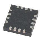
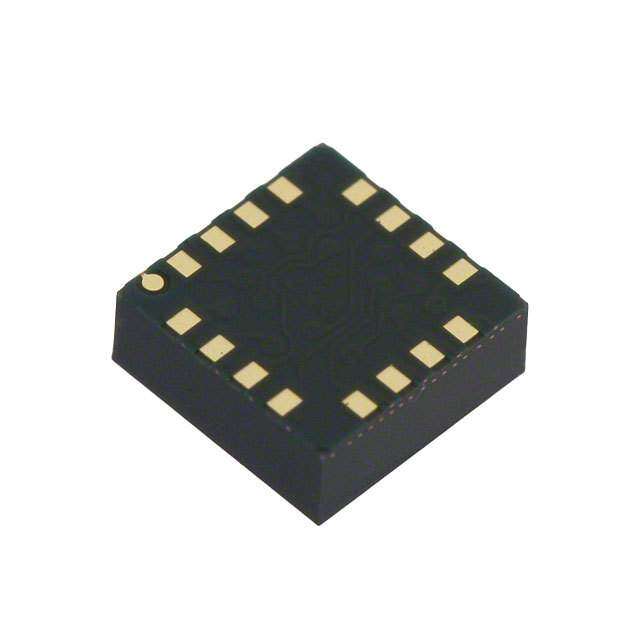
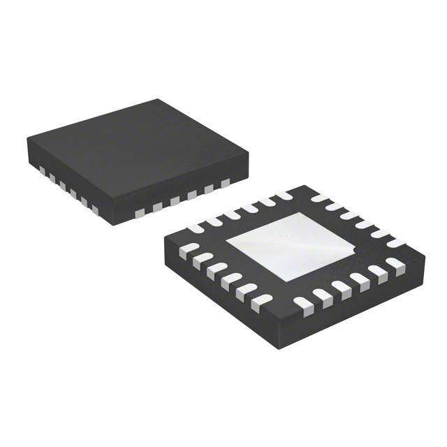
ICGOO电子元器件商城为您提供LIS344ALH由STMicroelectronics设计生产,在icgoo商城现货销售,并且可以通过原厂、代理商等渠道进行代购。 LIS344ALH价格参考¥34.31-¥34.31。STMicroelectronicsLIS344ALH封装/规格:运动传感器 - 加速计, Accelerometer X, Y, Z Axis ±2g, 6g 1.8kHz 16-LGA (4x4)。您可以下载LIS344ALH参考资料、Datasheet数据手册功能说明书,资料中有LIS344ALH 详细功能的应用电路图电压和使用方法及教程。
STMicroelectronics(意法半导体)的LIS344ALH是一款三轴加速度传感器,广泛应用于需要精确测量加速度或倾斜角度的场景。以下是该型号的主要应用场景:

1. 消费电子设备:
   - 用于智能手机、平板电脑和可穿戴设备(如智能手表、健身追踪器)中,实现步数计数、活动监测和手势识别功能。
   - 在游戏控制器中,提供基于运动的交互体验,例如方向控制或虚拟物体操作。

2. 工业自动化与监控:
   - 监测机械设备的振动情况,帮助预测故障并进行状态维护。
   - 用于机器人姿态控制,确保稳定性和精确动作。

3. 物联网(IoT)应用:
   - 集成到智能家居设备中,检测门窗开合状态或物品移动。
   - 用于资产跟踪系统,记录运输过程中货物的冲击或倾斜情况。

4. 医疗健康领域:
   - 在康复设备和健康监测仪器中,记录患者的运动数据以评估恢复进展。
   - 用于跌倒检测装置,及时报警以保障老年人安全。

5. 导航与定位:
   - 结合其他传感器(如陀螺仪或GPS),为惯性导航系统提供加速度数据。
   - 在无人机或自动驾驶车辆中,辅助姿态调整和路径规划。

6. 环境监测:
   - 用于地震监测设备,捕捉地面震动信息。
   - 检测建筑物或桥梁结构的稳定性变化,预防潜在风险。

LIS344ALH凭借其低功耗、高灵敏度和小型化设计,非常适合对空间和能耗有严格要求的应用场合,同时其三轴测量能力也为多维度运动分析提供了便利。
| 参数 | 数值 |
| 产品目录 | |
| 描述 | IC ACCELEROMETER 3AXIS 16LGA加速计 MEMS Inertial High Pef 3-Axis |
| 产品分类 | 加速计运动与定位传感器 |
| 品牌 | STMicroelectronics |
| 产品手册 | |
| 产品图片 |
|
| rohs | 符合RoHS无铅 / 符合限制有害物质指令(RoHS)规范要求 |
| 产品系列 | 加速计,STMicroelectronics LIS344ALH- |
| 数据手册 | |
| 产品型号 | LIS344ALH |
| 产品种类 | 加速计 |
| 传感轴 | X, Y, Z |
| 供应商器件封装 | 16-LGA(4x4) |
| 其它有关文件 | http://www.st.com/web/catalog/sense_power/FM89/SC444/PF207281?referrer=70071840 |
| 加速 | 2 g, 6 g |
| 加速度范围 | ±6g |
| 商标 | STMicroelectronics |
| 安装类型 | 表面贴装 |
| 封装 | Tray |
| 封装/外壳 | 16-LFLGA |
| 封装/箱体 | LGA-16 |
| 工厂包装数量 | 490 |
| 带宽 | 2kHz |
| 接口 | IC |
| 最大工作温度 | + 85 C |
| 最小工作温度 | - 40 C |
| 标准包装 | 490 |
| 灵敏度 | 0.100 x Vdd = V/g |
| 电压-电源 | 2.7 V ~ 3.3 V |
| 电源电压-最大 | 3.6 V |
| 电源电压-最小 | 2.4 V |
| 电源电流 | 680 uA |
| 系列 | LIS344ALH |
| 轴 | X,Y,Z |
| 输出类型 | 模拟 |


- 商务部:美国ITC正式对集成电路等产品启动337调查
- 曝三星4nm工艺存在良率问题 高通将骁龙8 Gen1或转产台积电
- 太阳诱电将投资9.5亿元在常州建新厂生产MLCC 预计2023年完工
- 英特尔发布欧洲新工厂建设计划 深化IDM 2.0 战略
- 台积电先进制程称霸业界 有大客户加持明年业绩稳了
- 达到5530亿美元!SIA预计今年全球半导体销售额将创下新高
- 英特尔拟将自动驾驶子公司Mobileye上市 估值或超500亿美元
- 三星加码芯片和SET,合并消费电子和移动部门,撤换高东真等 CEO
- 三星电子宣布重大人事变动 还合并消费电子和移动部门
- 海关总署:前11个月进口集成电路产品价值2.52万亿元 增长14.8%
.jpg)

PDF Datasheet 数据手册内容提取
LIS344ALH MEMS inertial sensor high performance 3-axis ±2/±6g ultracompact linear accelerometer Features ■ 2.4 V to 3.6 V single supply operation ■ ±2 g / ±6 g user selectable full-scale ■ Low power consumption ■ Output voltage, offset and sensitivity are ratiometric to the supply voltage ■ Factory trimmed device sensitivity and offset LGA 16L (4x4x1.5 mm) ■ Embedded self test ■ RoHS/ECOPACK® compliant ■ High shock survivability ( 10000 g ) The LIS344ALH has a dynamically user selectable full-scale of ±2 g / ±6 g and it is Description capable of measuring accelerations over a maximum bandwidth of 1.8 kHz for all axes. The The LIS344ALH is an ultra compact consumer device bandwidth may be reduced by using low-power three-axis linear accelerometer that external capacitances. The self-test capability includes a sensing element and an IC interface allows the user to check the functioning of the able to take the information from the sensing system. element and to provide an analog signal to the The LIS344ALH is available in Land Grid Array external world. package (LGA) manufactured by ST. The sensing element, capable of detecting the It is guaranteed to operate over an extended acceleration, is manufactured using a dedicated temperature range of -40 °C to +85 °C. process developed by ST to produce inertial The LIS344ALH belongs to a family of products sensors and actuators in silicon. suitable for a variety of applications: The IC interface is manufactured using an ST – Mobile terminals proprietary CMOS process with high level of – Gaming and virtual reality input devices integration. The dedicated circuit is trimmed to – Antitheft systems and inertial navigation better match the sensing element characteristics. – Appliance and robotics. Table 1. Device summary Order codes Temp range [°C] Package Packaging LIS344ALH -40 to +85 LGA-16L Tray LIS344ALHTR -40 to +85 LGA-16L Tape and reel April 2008 Rev 3 1/19 www.st.com 19
Content LIS344ALH Content 1 Block diagram and pin description . . . . . . . . . . . . . . . . . . . . . . . . . . . . . 5 1.1 Block diagram . . . . . . . . . . . . . . . . . . . . . . . . . . . . . . . . . . . . . . . . . . . . . . . 5 1.2 Pin description . . . . . . . . . . . . . . . . . . . . . . . . . . . . . . . . . . . . . . . . . . . . . . 5 2 Mechanical and electrical specifications . . . . . . . . . . . . . . . . . . . . . . . . 7 2.1 Mechanical characteristics . . . . . . . . . . . . . . . . . . . . . . . . . . . . . . . . . . . . . 7 2.2 Electrical characteristics . . . . . . . . . . . . . . . . . . . . . . . . . . . . . . . . . . . . . . . 8 2.3 Absolute maximum ratings . . . . . . . . . . . . . . . . . . . . . . . . . . . . . . . . . . . . . 9 2.4 Terminology . . . . . . . . . . . . . . . . . . . . . . . . . . . . . . . . . . . . . . . . . . . . . . . 10 3 Functionality . . . . . . . . . . . . . . . . . . . . . . . . . . . . . . . . . . . . . . . . . . . . . . 11 3.1 Sensing element . . . . . . . . . . . . . . . . . . . . . . . . . . . . . . . . . . . . . . . . . . . . 11 3.2 IC interface . . . . . . . . . . . . . . . . . . . . . . . . . . . . . . . . . . . . . . . . . . . . . . . . 11 3.3 Factory calibration . . . . . . . . . . . . . . . . . . . . . . . . . . . . . . . . . . . . . . . . . . 11 4 Application hints . . . . . . . . . . . . . . . . . . . . . . . . . . . . . . . . . . . . . . . . . . . 12 4.1 Soldering information . . . . . . . . . . . . . . . . . . . . . . . . . . . . . . . . . . . . . . . . 13 4.2 Output response vs orientation . . . . . . . . . . . . . . . . . . . . . . . . . . . . . . . . 13 5 Typical performance characteristics . . . . . . . . . . . . . . . . . . . . . . . . . . . 14 5.1 Mechanical characteristics at 25 °C . . . . . . . . . . . . . . . . . . . . . . . . . . . . . 14 5.2 Mechanical characteristics derived from measurement in the -40 °C to +85 °C temperature range . . . . . . . . . . . . . . . . . . . . . . . . . . . . . . . . . . . . . . . . 15 5.3 Electrical characteristics at 25 °C . . . . . . . . . . . . . . . . . . . . . . . . . . . . . . . 16 6 Package information . . . . . . . . . . . . . . . . . . . . . . . . . . . . . . . . . . . . . . . . 17 7 Revision history . . . . . . . . . . . . . . . . . . . . . . . . . . . . . . . . . . . . . . . . . . . 18 2/19
LIS344ALH List of figures List of figures Figure 1. Block diagram. . . . . . . . . . . . . . . . . . . . . . . . . . . . . . . . . . . . . . . . . . . . . . . . . . . . . . . . . . . . 5 Figure 2. Pin connection . . . . . . . . . . . . . . . . . . . . . . . . . . . . . . . . . . . . . . . . . . . . . . . . . . . . . . . . . . . 5 Figure 3. LIS344ALH electrical connection . . . . . . . . . . . . . . . . . . . . . . . . . . . . . . . . . . . . . . . . . . . . 12 Figure 4. Output response vs orientation. . . . . . . . . . . . . . . . . . . . . . . . . . . . . . . . . . . . . . . . . . . . . . 13 Figure 5. X axis Zero-g level at 3.3 V . . . . . . . . . . . . . . . . . . . . . . . . . . . . . . . . . . . . . . . . . . . . . . . . 14 Figure 6. X axis Sensitivity at 3.3 V. . . . . . . . . . . . . . . . . . . . . . . . . . . . . . . . . . . . . . . . . . . . . . . . . . 14 Figure 7. Y axis Zero-g level at 3.3 V. . . . . . . . . . . . . . . . . . . . . . . . . . . . . . . . . . . . . . . . . . . . . . . . . 14 Figure 8. Y axis Sensitivity at 3.3 V. . . . . . . . . . . . . . . . . . . . . . . . . . . . . . . . . . . . . . . . . . . . . . . . . . 14 Figure 9. Z axis Zero-g level at 3.3 V. . . . . . . . . . . . . . . . . . . . . . . . . . . . . . . . . . . . . . . . . . . . . . . . . 14 Figure 10. Z axis Sensitivity at 3.3 V . . . . . . . . . . . . . . . . . . . . . . . . . . . . . . . . . . . . . . . . . . . . . . . . . . 14 Figure 11. X axis Zero-g level change vs. temperature at 3.3 V . . . . . . . . . . . . . . . . . . . . . . . . . . . . . 15 Figure 12. X axis Sensitivity change vs. temperature at 3.3 V. . . . . . . . . . . . . . . . . . . . . . . . . . . . . . . 15 Figure 13. Y axis Zero-g level change vs. temperature at 3.3 V . . . . . . . . . . . . . . . . . . . . . . . . . . . . . 15 Figure 14. Y axis Sensitivity change vs. temperature at 3.3 V. . . . . . . . . . . . . . . . . . . . . . . . . . . . . . . 15 Figure 15. Z axis Zero-g level change vs. temperature at 3.3 V . . . . . . . . . . . . . . . . . . . . . . . . . . . . . 15 Figure 16. Z axis Sensitivity change vs. temperature at 3.3 V. . . . . . . . . . . . . . . . . . . . . . . . . . . . . . . 15 Figure 17. Current consumption in normal mode at 3.3 V. . . . . . . . . . . . . . . . . . . . . . . . . . . . . . . . . . 16 Figure 18. Current consumption in power-down at 3.3 V. . . . . . . . . . . . . . . . . . . . . . . . . . . . . . . . . . . 16 Figure 19. Noise density at 3.3 V (X, Y axis). . . . . . . . . . . . . . . . . . . . . . . . . . . . . . . . . . . . . . . . . . . . 16 Figure 20. Noise density at 3.3 V (Z axis) . . . . . . . . . . . . . . . . . . . . . . . . . . . . . . . . . . . . . . . . . . . . . . 16 Figure 21. LGA 16: mechanical data and package dimensions. . . . . . . . . . . . . . . . . . . . . . . . . . . . . . 17 3/19
List of tables LIS344ALH List of tables Table 1. Device summary. . . . . . . . . . . . . . . . . . . . . . . . . . . . . . . . . . . . . . . . . . . . . . . . . . . . . . . . . . 1 Table 2. Pin description . . . . . . . . . . . . . . . . . . . . . . . . . . . . . . . . . . . . . . . . . . . . . . . . . . . . . . . . . . . 6 Table 3. Mechanical characteristics @ Vdd =3.3 V, T = 25 °C unless otherwise noted. . . . . . . . . . . 7 Table 4. Electrical characteristics @ Vdd =3.3 V, T = 25 °C unless otherwise noted. . . . . . . . . . . . . 8 Table 5. Absolute maximum ratings. . . . . . . . . . . . . . . . . . . . . . . . . . . . . . . . . . . . . . . . . . . . . . . . . . 9 Table 6. Filter capacitor selection, C (x, y, z),. . . . . . . . . . . . . . . . . . . . . . . . . . . . . . . . . . . . . . . 13 load Table 7. Document revision history . . . . . . . . . . . . . . . . . . . . . . . . . . . . . . . . . . . . . . . . . . . . . . . . . 18 4/19
LIS344ALH Block diagram and pin description 1 Block diagram and pin description 1.1 Block diagram Figure 1. Block diagram X+ Routx VoutX CHARGE S/H Y+ AMPLIFIER Z+ a Routy VoutY MUX DEMUX S/H Z- Y- X- Routz VoutZ S/H SELF TEST REFERENCE TRIMMING CIRCUIT CLOCK 1.2 Pin description Figure 2. Pin connection Z N V R N C d e C d s 13 16 1 VoutX 12 1 FS NC ST VoutY NC Y NC 9 4 Res X 8 5 V G N P o N C D (TOP VIEW) utZ D DIRECTIONS OF THE (BOTTOM VIEW) DETECTABLE ACCELERATIONS 5/19
Block diagram and pin description LIS344ALH T able 2. Pin description Pin # Pin name Function 1 FS Full scale selection (logic 0: ±2g full-scale; logic 1: ±6g full-scale) 2 ST Self test (logic 0: normal mode; logic 1: self-test mode) 3 NC Internally not connected 4 Res Leave unconnected or connect to Vdd 5 PD Power down (logic 0: normal mode; logic 1: power-down mode) 6 NC Internally not connected 7 GND 0 V supply 8 VoutZ Output voltage Z channel 9 NC Internally not connected 10 VoutY Output voltage Y channel 11 NC Internally not connected 12 VoutX Output voltage X channel 13 NC Internally not connected 14 Vdd Power supply 15 Res Connect to Vdd 16 NC Internally not connected 6/19
LIS344ALH Mechanical and electrical specifications 2 Mechanical and electrical specifications 2.1 Mechanical characteristics Table 3. Mechanical characteristics @ Vdd =3.3 V, T = 25 °C unless otherwise noted(1) Symbol Parameter Test condition Min. Typ.(2) Max. Unit FS pin connected to ±1.8 ± 2 Ar Acceleration range(3) GND g FS pin connected to Vdd ±5.4 ± 6 Full-scale = ±2 g Vdd/5 - 5% Vdd/5 Vdd/5 + 5% So Sensitivity(4) V/g Full-scale = ±6 g Vdd/15 - 10% Vdd/15 Vdd/15 + 10% Sensitivity change Vs SoDr Delta from +25 °C ± 0.01 %/°C Temperature Full-scale = ±2 g Voff Zero-g level(4) Vdd/2 - 5% Vdd/2 Vdd/2 + 5% V T = 25 °C Zero-g level change Vs OffDr Delta from +25 °C ±0.4 mg/°C Temperature Best fit straight line NL Non linearity(5) ±0.5 % FS Full-scale = ±2 g CrossAx Cross-axis(6) ±2 % Acceleration noise Vdd = 3.3 V; An 50 µg/ Hz density Full-scale = ±2 g X axis 80 140 200 mV T = 25 °C; Vdd=3.3 V Self test output voltage Y axis Vt -200 -140 -80 mV change(7),(8),(9) T = 25 °C; Vdd=3.3 V Z axis 100 230 350 mV T = 25 °C; Vdd=3.3 V Sensing element Fres X,Y,Z axis 1.8 KHz resonant frequency(10) Operating temperature Top -40 +85 °C range Wh Product weight 0.040 gram 1. The product is factory calibrated at 3.3 V. The operational power supply range is from 2.4 V to 3.6 V. Voff, So and Vt parameters will vary with supply voltage. 2. Typical specifications are not guaranteed. 3. Guaranteed by wafer level test and measurement of initial offset and sensitivity. 4. Zero-g level and sensitivity are essentially ratiometric to supply voltage at the calibration level ±8%. 5. Guaranteed by design. 6. Contribution to the measuring output of an inclination/acceleration along any perpendicular axis. 7. “Self test output voltage change” is defined as Vout -Vout . (Vst=Logic1) (Vst=Logic0) 8. “Self test output voltage change” varies cubically with supply voltage. 9. When full-scale is set to ±6 g, “Self test output voltage change” is one third of the specified value at ±2 g. 10. Minimum resonance frequency Fres=1.8 kHz. Sensor bandwidth=1/(2*π*110kΩ*Cload), with Cload>1 nF. 7/19
Mechanical and electrical specifications LIS344ALH 2.2 Electrical characteristics Table 4. Electrical characteristics @ Vdd =3.3 V, T = 25 °C unless otherwise noted(1) Symbol Parameter Test condition Min. Typ.(2) Max. Unit Vdd Supply voltage 2.4 3.3 3.6 V Normal mode 680 850 Idd Supply current µA Power-down mode 1 5 Vfs Full-scale input Logic 0 level 0 0.3*Vdd V Vst Self-test input Vpd Power-down input Logic 1 level 0.7*Vdd Vdd V Output impedance of Rout 90 110 130 KΩ VoutX, VoutY, VoutZ Capacitive load drive(3) Cload 1 nF for VoutX, VoutY, VoutZ Turn-on time at exit of 550*Cload+ Ton Cload expressed in µF ms Power-down mode 0.3 Operating temperature Top -40 +85 ºC range 1. The product is factory calibrated at 3.3 V. 2. Typical specifications are not guaranteed. 3. Minimum resonance frequency Fres=1.8 kHz. Device bandwidth=1/(2*π*110 kΩ*Cload), with Cload>1 nF. 8/19
LIS344ALH Mechanical and electrical specifications 2.3 Absolute maximum ratings Stresses above those listed as “Absolute maximum ratings” may cause permanent damage to the device. This is a stress rating only and functional operation of the device under these conditions is not implied. Exposure to maximum rating conditions for extended periods may affect device reliability. Table 5. Absolute maximum ratings Symbol Ratings Maximum value Unit Vdd Supply voltage -0.3 to 7 V Vin Input voltage on any control pin (FS, ST, PD) -0.3 to Vdd +0.3 V 3000 g for 0.5 ms A Acceleration (any axis, powered, Vdd = 3.3 V) POW 10000 g for 0.1 ms 3000 g for 0.5 ms A Acceleration (any axis, not powered) UNP 10000 g for 0.1 ms T Storage temperature range -40 to +125 °C STG 4 (HBM) KV ESD Electrostatic discharge protection 1.5 (CDM) KV 400 (MM) V This is a mechanical shock sensitive device, improper handling can cause permanent damages to the part This is an ESD sensitive device, improper handling can cause permanent damages to the part 9/19
Mechanical and electrical specifications LIS344ALH 2.4 Terminology Sensitivity describes the gain of the sensor and can be determined by applying 1g acceleration to it. As the sensor can measure DC accelerations this can be done easily by pointing the axis of interest towards the center of the Earth, note the output value, rotate the sensor by 180 degrees (point to the sky) and note the output value again thus applying ±1g acceleration to the sensor. Subtracting the larger output value from the smaller one, and dividing the result by 2, will give the actual sensitivity of the sensor. This value changes very little over temperature (see sensitivity change vs temperature) and also very little over time. The Sensitivity tolerance describes the range of sensitivities of a large population of sensors. Zero-g level describes the actual output signal if there is no acceleration present. A sensor in a steady state on a horizontal surface will measure 0 g in X axis and 0 g in Y axis whereas the Z axis will measure 1g. The output is ideally for a 3.3 V powered sensor Vdd/2 = 1650 mV. A deviation from ideal 0-g level (1650 mV in this case) is called Zero-g offset. Offset of precise MEMS sensors is to some extend a result of stress to the sensor and therefore the offset can slightly change after mounting the sensor onto a printed circuit board or exposing it to extensive mechanical stress. Offset changes little over temperature - see “Zero-g level change vs temperature” - the Zero-g level of an individual sensor is very stable over lifetime. The Zero-g level tolerance describes the range of Zero-g levels of a population of sensors. Self test allows to test the mechanical and electric part of the sensor, allowing the seismic mass to be moved by means of an electrostatic test-force. The Self Test function is off when the ST pin is connected to GND. When the ST pin is tied at Vdd an actuation force is applied to the sensor, simulating a definite input acceleration. In this case the sensor outputs will exhibit a voltage change in their DC levels which is related to the selected full-scale and depending on the supply voltage through the device sensitivity. When ST is activated, the device output level is given by the algebraic sum of the signals produced by the acceleration acting on the sensor and by the electrostatic test-force. If the output signals change within the amplitude specified inside Table3, then the sensor is working properly and the parameters of the interface chip are within the defined specification. Output impedance describes the resistor inside the output stage of each channel. This resistor is part of a filter consisting of an external capacitor of at least 1 nF and the internal resistor. Due to the high resistor level, only small inexpensive external capacitors are needed to generate low corner frequencies. When interfacing with an ADC it is important to use high input impedance input circuitries to avoid measurement errors. Note that the minimum load capacitance forms a corner frequency close to the resonance frequency of the sensor. In general the smallest possible bandwidth for a particular application should be chosen to get the best results. 10/19
LIS344ALH Functionality 3 Functionality The LIS344ALH is an ultra compact low-power, analog output three-axis linear accelerometer packaged in a LGA package. The complete device includes a sensing element and an IC interface able to take the information from the sensing element and to provide an analog signal to the external world. 3.1 Sensing element A proprietary process is used to create a surface micro-machined accelerometer. The technology allows to carry out suspended silicon structures which are attached to the substrate in a few points called anchors and are free to move in the direction of the sensed acceleration. To be compatible with the traditional packaging techniques a cap is placed on top of the sensing element to avoid blocking the moving parts during the moulding phase of the plastic encapsulation. When an acceleration is applied to the sensor the proof mass displaces from its nominal position, causing an imbalance in the capacitive half-bridge. This imbalance is measured using charge integration in response to a voltage pulse applied to the sense capacitor. At steady state the nominal value of the capacitors are few pF and when an acceleration is applied the maximum variation of the capacitive load is in the fF range. 3.2 IC interface The complete signal processing uses a fully differential structure, while the final stage converts the differential signal into a single-ended one to be compatible with the external world. The first stage is a low-noise capacitive amplifier that implements a Correlated Double Sampling (CDS) at its output to cancel the offset and the 1/f noise. The produced signal is then sent to three different S&Hs, one for each channel, and made available to the outside. All the analog parameters (output offset voltage and sensitivity) are ratiometric to the voltage supply. Increasing or decreasing the voltage supply, the sensitivity and the offset will increase or decrease linearly. This feature provides the cancellation of the error related to the voltage supply along an analog to digital conversion chain. 3.3 Factory calibration The IC interface is factory calibrated for sensitivity (So) and Zero-g level (Voff). The trimming values are stored inside the device by a non volatile structure. Any time the device is turned on, the trimming parameters are downloaded into the registers to be employed during the normal operation. This allows the user to employ the device without further calibration. 11/19
Application hints LIS344ALH 4 Application hints Figure 3. LIS344ALH electrical connection GND GND Vdd 100nF 10µF Z 16 15 14 13 1 FS Optional Pin 1 indicator 1 12 Vout x ST Cload X 2 LIS344ALH 11 Optional Y 3 (top view) 10 Vout y Cload Y X 4 9 5 6 7 8 (TOP VIEW) Optional DIRECTIONS OF THE Vout z D DETECTABLE P Cload Z ACCELERATIONS GND Digital signals Power supply decoupling capacitors (100 nF ceramic or polyester + 10 µF Aluminum) should be placed as near as possible to the device (common design practice). The LIS344ALH allows to band limit VoutX, VoutY and VoutZ through the use of external capacitors. The recommended frequency range spans from DC up to 1.8 kHz. In particular, capacitors are added at output VoutX, VoutY, VoutZ pins to implement low-pass filtering for antialiasing and noise reduction. The equation for the cut-off frequency (f) of the external t filters is in this case: 1 f = ------------------------------------------------------------------------- t 2π⋅ R ⋅ C (x, y, z) out load Taking into account that the internal filtering resistor (R ) has a nominal value equal to out 110 KΩ, the equation for the external filter cut-off frequency may be simplified as follows: 1.45µF f = ---------------------------------------[Hz] t C (x, y, z) load The tolerance of the internal resistor can vary typically of ±20% within its nominal value of 110 KΩ; thus the cut-off frequency will vary accordingly. A minimum capacitance of 1 nF for C (x, y, z) is required. load 12/19
LIS344ALH Application hints T able 6. Filter capacitor selection, C (x, y, z), load Cut-off frequency Capacitor value 1 Hz 1500 nF 10 Hz 150 nF 20 Hz 68 nF 50 Hz 30 nF 100 Hz 15 nF 200 Hz 6.8 nF 500 Hz 3 nF 4.1 Soldering information The LGA package is compliant with the ECOPACK, RoHS and “Green” standard. It is qualified for soldering heat resistance according to JEDEC J-STD-020C. Leave “Pin 1 Indicator” unconnected during soldering. Land pattern and soldering recommendations are available at www.st.com/mems. 4.2 Output response vs orientation Figure 4. Output response vs orientation Bottom X=2.31V (+1g) X=1.65V (0g) X=1.65V (0g) Y=1.65V (0g) Y=2.31V (+1g) Y=1.65V (0g) Z=1.65V (0g) Z=1.65V (0g) Top Z=0.99V (-1g) Top X=1.65V (0g) X=1.65V (0g) X=0.99V (-1g) Y=0.99V (-1g) Y=1.65V (0g) Y=1.65V (0g) Z=1.65V (0g) Z=1.65V (0g) Bottom Z=2.31V (+1g) Earth’s Surface Figure4 shows output voltage values of LIS344ALH, powered at 3.3 V, with full-scale ±2 g. 13/19
Typical performance characteristics LIS344ALH 5 Typical performance characteristics 5.1 Mechanical characteristics at 25 °C Figure 5. X axis Zero-g level at 3.3 V Figure 6. X axis Sensitivity at 3.3 V 30 16 14 25 12 Percent of parts [%]112050 Percent of parts [%]1680 4 5 2 0 0 1.6 1.61 1.62 1.63 1.64 1.65 1.66 1.67 1.68 1.69 1.7 0.62 0.63 0.64 0.65 0.66 0.67 0.68 0.69 0.7 Zero−g Level Offset [V] Sensitivity [V/g] Figure 7. Y axis Zero-g level at 3.3 V Figure 8. Y axis Sensitivity at 3.3 V 25 15 20 %] %]10 Percent of parts [1105 Percent of parts [ 5 5 0 0 1.6 1.61 1.62 1.63 1.64 1.65 1.66 1.67 1.68 1.69 1.7 0.62 0.63 0.64 0.65 0.66 0.67 0.68 0.69 0.7 Zero−g Level Offset [V] Sensitivity [V/g] Figure 9. Z axis Zero-g level at 3.3 V Figure 10. Z axis Sensitivity at 3.3 V 25 14 12 20 10 %] %] Percent of parts [1105 Percent of parts [ 68 4 5 2 0 0 1.6 1.61 1.62 1.63 1.64 1.65 1.66 1.67 1.68 1.69 1.7 0.62 0.63 0.64 0.65 0.66 0.67 0.68 0.69 0.7 Zero−g Level Offset [V] Sensitivity [V/g] 14/19
LIS344ALH Typical performance characteristics 5.2 Mechanical characteristics derived from measurement in the -40 °C to +85 °C temperature range Figure 11. X axis Zero-g level change Figure 12. X axis Sensitivity change vs. temperature at 3.3 V vs. temperature at 3.3 V 40 60 35 50 30 Percent of parts [%]122505 Percent of parts [%]234000 10 10 5 0 0 −4 −3 −2 −1 0 1 2 3 4 −0.1 −0.08 −0.06 −0.04 −0.02 0 0.02 0.04 0.06 0.08 0.1 Zero−g Level drift [mg/oC] Sensitivity drift [%/oC] Figure 13. Y axis Zero-g level change Figure 14. Y axis Sensitivity change vs. temperature at 3.3 V vs. temperature at 3.3 V 45 45 40 40 35 35 %]30 %]30 Percent of parts [122505 Percent of parts [122505 10 10 5 5 0 0 −4 −3 −2 −1 0 1 2 3 4 −0.1 −0.08 −0.06 −0.04 −0.02 0 0.02 0.04 0.06 0.08 0.1 Zero−g Level drift [mg/oC] Sensitivity drift [%/oC] Figure 15. Z axis Zero-g level change Figure 16. Z axis Sensitivity change vs. temperature at 3.3 V vs. temperature at 3.3 V 35 40 30 35 30 25 Percent of parts [%]1250 Percent of parts [%]122505 10 10 5 5 0 0 −4 −3 −2 −1 0 1 2 3 4 −0.1 −0.08 −0.06 −0.04 −0.02 0 0.02 0.04 0.06 0.08 0.1 Zero−g Level drift [mg/oC] Sensitivity drift [%/oC] 15/19
Typical performance characteristics LIS344ALH 5.3 Electrical characteristics at 25 °C Figure 17. Current consumption Figure 18. Current consumption in normal mode at 3.3 V in power-down at 3.3 V 30 45 40 25 35 %]20 %]30 Percent of parts [1105 Percent of parts [122505 10 5 5 0 0 450 500 550 600 650 700 750 800 850 900 −4 −3 −2 −1 0 1 2 3 4 Current consumption [uA] Current consumption [uA] Figure 19. Noise density at 3.3 V (X, Y axis) Figure 20. Noise density at 3.3 V (Z axis) 30 30 25 25 20 20 %] %] Frequency of parts [15 Frequency of parts [15 10 10 5 5 0 0 18 20 22 24 26 28 30 32 10 20 30 40 50 60 70 80 Noise Density [/mug/sqrt(Hz)] Noise Density [/mug/sqrt(Hz)] 16/19
LIS344ALH Package information 6 Package information In order to meet environmental requirements, ST offers these devices in ECOPACK® packages. These packages have a lead-free second level interconnect. The category of second level Interconnect is marked on the inner box label, in compliance with JEDEC Standard JESD97. The maximum ratings related to soldering conditions are also marked on the inner box label. ECOPACK® is an ST trademark. ECOPACK® specifications are available at: www.st.com. Figure 21. LGA 16L: mechanical data and package dimensions Dimensions mm inch Outline and Ref. Min. Typ. Max. Min. Typ. Max. mechanical data A1 1.500 1.600 0.0591 0.0630 A2 1.330 0.0524 A3 0.160 0.200 0.240 0.0063 0.0079 0.0094 d 0.300 0.0118 D1 3.850 4.000 4.150 0.1516 0.1575 0.1634 E1 3.850 4.000 4.150 0.1516 0.1575 0.1634 L2 1.950 0.0768 M 0.100 0.0039 N1 0.650 0.0256 N2 0.975 0.0384 P1 1.750 0.0689 P2 1.525 0.0600 LGA 16L (4x4x1.5mm) T1 0.400 0.0157 Land Grid Array Package T2 0.300 0.0118 k 0.050 0.0020 7974136 17/19
Revision history LIS344ALH 7 Revision history T able 7. Document revision history Date Revision Changes 15-Jan-2008 1 Initial release. 18-Feb-2008 2 Minor text changes Updated Section2: Mechanical and electrical specifications and 29-Apr-2008 3 added distribution graphs in Section5: Typical performance characteristics 18/19
LIS344ALH Please Read Carefully: Information in this document is provided solely in connection with ST products. STMicroelectronics NV and its subsidiaries (“ST”) reserve the right to make changes, corrections, modifications or improvements, to this document, and the products and services described herein at any time, without notice. All ST products are sold pursuant to ST’s terms and conditions of sale. Purchasers are solely responsible for the choice, selection and use of the ST products and services described herein, and ST assumes no liability whatsoever relating to the choice, selection or use of the ST products and services described herein. No license, express or implied, by estoppel or otherwise, to any intellectual property rights is granted under this document. If any part of this document refers to any third party products or services it shall not be deemed a license grant by ST for the use of such third party products or services, or any intellectual property contained therein or considered as a warranty covering the use in any manner whatsoever of such third party products or services or any intellectual property contained therein. UNLESS OTHERWISE SET FORTH IN ST’S TERMS AND CONDITIONS OF SALE ST DISCLAIMS ANY EXPRESS OR IMPLIED WARRANTY WITH RESPECT TO THE USE AND/OR SALE OF ST PRODUCTS INCLUDING WITHOUT LIMITATION IMPLIED WARRANTIES OF MERCHANTABILITY, FITNESS FOR A PARTICULAR PURPOSE (AND THEIR EQUIVALENTS UNDER THE LAWS OF ANY JURISDICTION), OR INFRINGEMENT OF ANY PATENT, COPYRIGHT OR OTHER INTELLECTUAL PROPERTY RIGHT. UNLESS EXPRESSLY APPROVED IN WRITING BY AN AUTHORIZED ST REPRESENTATIVE, ST PRODUCTS ARE NOT RECOMMENDED, AUTHORIZED OR WARRANTED FOR USE IN MILITARY, AIR CRAFT, SPACE, LIFE SAVING, OR LIFE SUSTAINING APPLICATIONS, NOR IN PRODUCTS OR SYSTEMS WHERE FAILURE OR MALFUNCTION MAY RESULT IN PERSONAL INJURY, DEATH, OR SEVERE PROPERTY OR ENVIRONMENTAL DAMAGE. ST PRODUCTS WHICH ARE NOT SPECIFIED AS "AUTOMOTIVE GRADE" MAY ONLY BE USED IN AUTOMOTIVE APPLICATIONS AT USER’S OWN RISK. Resale of ST products with provisions different from the statements and/or technical features set forth in this document shall immediately void any warranty granted by ST for the ST product or service described herein and shall not create or extend in any manner whatsoever, any liability of ST. ST and the ST logo are trademarks or registered trademarks of ST in various countries. Information in this document supersedes and replaces all information previously supplied. The ST logo is a registered trademark of STMicroelectronics. All other names are the property of their respective owners. © 2008 STMicroelectronics - All rights reserved STMicroelectronics group of companies Australia - Belgium - Brazil - Canada - China - Czech Republic - Finland - France - Germany - Hong Kong - India - Israel - Italy - Japan - Malaysia - Malta - Morocco - Singapore - Spain - Sweden - Switzerland - United Kingdom - United States of America www.st.com 19/19
Mouser Electronics Authorized Distributor Click to View Pricing, Inventory, Delivery & Lifecycle Information: S TMicroelectronics: LIS344ALH LIS344ALHTR