ICGOO在线商城 > 传感器,变送器 > 运动传感器 - 加速计 > MMA9550LR1

 Datasheet下载
- 型号: MMA9550LR1
- 制造商: Freescale Semiconductor
- 库位|库存: xxxx|xxxx
- 要求:
| 数量阶梯 | 香港交货 | 国内含税 |
| +xxxx | $xxxx | ¥xxxx |
查看当月历史价格
查看今年历史价格
MMA9550LR1产品简介:
ICGOO电子元器件商城为您提供MMA9550LR1由Freescale Semiconductor设计生产,在icgoo商城现货销售,并且可以通过原厂、代理商等渠道进行代购。 MMA9550LR1价格参考。Freescale SemiconductorMMA9550LR1封装/规格:运动传感器 - 加速计, Accelerometer X, Y, Z Axis ±2g, 4g, 8g 1.9Hz ~ 244Hz 16-LGA (3x3)。您可以下载MMA9550LR1参考资料、Datasheet数据手册功能说明书,资料中有MMA9550LR1 详细功能的应用电路图电压和使用方法及教程。
NXP USA Inc. 生产的MMA9550LR1是一款高性能的运动传感器,主要用作加速计。该型号广泛应用于多种场景,尤其在需要精确测量加速度和倾斜角度的设备中表现出色。

 1. 智能手机和平板电脑
MMA9550LR1可以用于智能手机和平板电脑中,实现屏幕自动旋转、步数计数、游戏控制等功能。它能够检测设备的姿态变化,从而优化用户体验。

 2. 可穿戴设备
在智能手表、健身追踪器等可穿戴设备中,MMA9550LR1可以监测用户的运动状态,如跑步、步行、爬楼梯等,并记录步数、距离、消耗的卡路里等数据。此外,它还可以用于跌倒检测,及时发出警报。

 3. 汽车电子
该加速计可用于汽车的安全系统,如碰撞检测、气囊触发等。它能够实时监测车辆的加速度变化,确保在发生碰撞时迅速响应。此外,MMA9550LR1也可以用于车辆的倾斜角度检测,帮助驾驶员了解车辆的状态,提高行车安全。

 4. 工业自动化
在工业环境中,MMA9550LR1可以用于振动监测,帮助检测机械设备的运行状态。通过分析振动数据,可以提前发现潜在的故障,进行预防性维护,减少停机时间。

 5. 物联网(IoT)设备
MMA9550LR1可以集成到各种物联网设备中,如智能家居传感器、环境监测设备等。它可以检测物体的移动或倾斜,触发相应的事件,如报警、通知等,增强系统的智能化水平。

 6. 医疗健康
在医疗领域,MMA9550LR1可以用于康复设备、老年人护理设备等。它可以监测患者的活动情况,提供运动数据分析,帮助医生评估康复效果。此外,它还可以用于睡眠监测,记录用户的翻身次数、睡眠姿势等信息。

总之,MMA9550LR1凭借其高精度和低功耗的特点,在多个领域都有广泛的应用前景,为各类设备提供了可靠的运动感知能力。
| 参数 | 数值 |
| 产品目录 | |
| 描述 | IC ACCEL 3-AXIS W/32B MCU 16LGA加速计 3-AXIS low g |
| 产品分类 | 加速计运动与定位传感器 |
| 品牌 | Freescale Semiconductor |
| 产品手册 | |
| 产品图片 |
|
| rohs | RoHS 合规性豁免无铅 / 符合限制有害物质指令(RoHS)规范要求 |
| 产品系列 | 加速计,Freescale Semiconductor MMA9550LR1- |
| 数据手册 | |
| 产品型号 | MMA9550LR1 |
| 产品种类 | 加速计 |
| 传感轴 | Triple |
| 供应商器件封装 | 16-LGA(3x3) |
| 其它名称 | MMA9550LR1DKR |
| 分辨率 | 32 bit |
| 加速度范围 | ±2g, 4g, 8g |
| 单位重量 | 19.700 mg |
| 商标 | Freescale Semiconductor |
| 商标名 | Xtrinsic |
| 安装类型 | 表面贴装 |
| 封装 | Reel |
| 封装/外壳 | 16-VFLGA |
| 封装/箱体 | LGA-16 |
| 工厂包装数量 | 1000 |
| 带宽 | - |
| 接口 | I2C, SPI |
| 数字输出-位数 | 32 bit |
| 数字输出-总线接口 | I2C, SPI |
| 标准包装 | 1 |
| 灵敏度 | 0.061mg/LSB,0.122mg/LSB,0.244mg/LSB |
| 电压-电源 | 1.71 V ~ 1.89 V |
| 电源电压-最大 | 2 V |
| 电源电压-最小 | - 0.3 V |
| 电源电流 | 2 uA |
| 轴 | X,Y,Z |
| 输出类型 | Digital |


- 商务部:美国ITC正式对集成电路等产品启动337调查
- 曝三星4nm工艺存在良率问题 高通将骁龙8 Gen1或转产台积电
- 太阳诱电将投资9.5亿元在常州建新厂生产MLCC 预计2023年完工
- 英特尔发布欧洲新工厂建设计划 深化IDM 2.0 战略
- 台积电先进制程称霸业界 有大客户加持明年业绩稳了
- 达到5530亿美元!SIA预计今年全球半导体销售额将创下新高
- 英特尔拟将自动驾驶子公司Mobileye上市 估值或超500亿美元
- 三星加码芯片和SET,合并消费电子和移动部门,撤换高东真等 CEO
- 三星电子宣布重大人事变动 还合并消费电子和移动部门
- 海关总署:前11个月进口集成电路产品价值2.52万亿元 增长14.8%

PDF Datasheet 数据手册内容提取
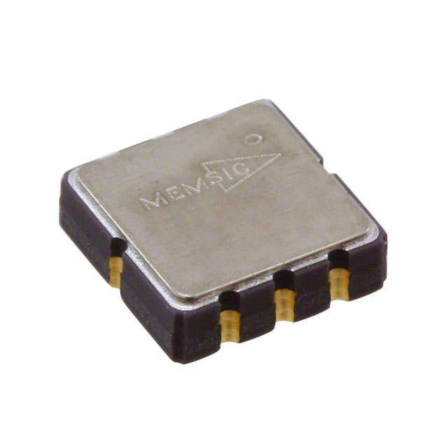
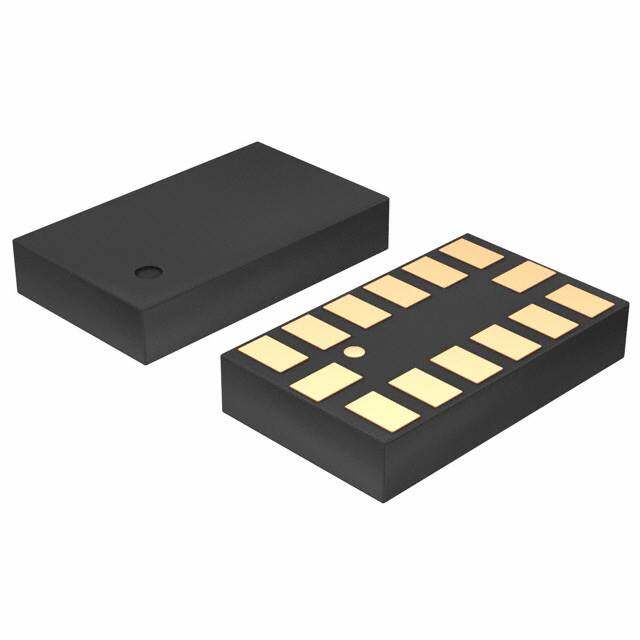
Freescale Semiconductor Document Number: MMA955xL Data Sheet: Technical Data Rev. 3.1, 5/2015 An Energy Efficient Solution by Freescale MMA955xL Intelligent MMA9550L Motion-Sensing Platform MMA9551L The MMA955xL device an intelligent sensor, incorporating dedicated MMA9553L accelerometer MEMS transducers, signal conditioning, data conversion, and a 32-bit programmable microcontroller. MMA9559L This unique blend transforms Freescale’s MMA955xL into an intelligent, high- precision, motion-sensing platform able to manage multiple sensor inputs. This device can make system-level decisions required for sophisticated applications Top and bottom view such as gesture recognition, pedometer functionality, tilt compensation and calibration, and activity monitoring. The MMA955xL device is programmed and configured with the CodeWarrior Development Studio for Microcontrollers software, version 10.1 or later. This standard integrated design environment enables customers to quickly implement custom algorithms and features to exactly match their application needs. Using the master I2C port, the MMA955xL device can manage secondary sensors, such as pressure sensors, magnetometers, or gyroscopes. This allows sensor initialization, calibration, data compensation, and computation 16-pin LGA functions to be off-loaded from the system application processor. The 3 mm x 3 mm x 1 mm MMA955xL device also acts as an intelligent sensing hub and a highly Case 2094-01 configurable decision engine. Total system power consumption is significantly reduced because the application processor stays powered down until Top view absolutely needed. Hardware Features _B B D • Three accelerometer operating ranges: P 8/ – ±fr2eegf aslul.i tFso mr otaspt hdaentedc gtieosnt,u ±re4sg ( oarniedn ±ta8tigo na rdee tseucptipoonr taendd. tilt control) and VSSA RGPIO VDDA –– ±±48gg cdoevteecrsts mmoosstt raebgruulaprt ahcutmivaitnie sd y(ngaammiicnsg )(walking and jogging) VDD 1 16 15 14 13 RTPGMPCIOH71/AN1/ • Integrated temperature sensor B/KRGGDP-IMOS9 2 12 RTPGMPCIOH60/AN0 • One slave SPI or I2C interface operating at up to 2Mbps, dedicated to RESETB 3 11 RGPIO5/PDB_A/ INT_O communication with the host processor. Default value of the I2C, 7-bit SCL0/RGPIO0 4 SCLK 10 VSS address is 0x4C. (This can be customized by firmware.) VSS 5 9 RGPIO4/INT • One master I2C interface operating at up to 400kbps that can be used to 6 7 8 • Ecfaoirgmthhmte sru efnrleoiccmatat e3b 9lwe0i 6tohuH etpzxu tteto dr n0aa.t2al 4 sreaHntezs sow (riOsthD MRM), Afr9o5m5 498L8 FHirmz twoa 3r.e8 vHezrs (ieoxnt)ending GPIO1/SDI SCL1/SDO SDA1/SSB • 10, 12, 14, and 16-bit trimmed ADC data formats available 0/R O2/ O3/ • 1.8V supply voltage SDA RGPI RGPI • 32-bit CPU with MAC unit Pin connections • Extensive set of power-management features and low-power modes • Integrated 16-bit resolution ADC can be used to convert external analog signals • Single-Wire, Background-Debug Mode (BDM) pin interface • 16-KB flash memory • 2-KB Random Access Memory • ROM-based flash controller and slave-port, command-line interpreter • Two-channel timer with input capture, output capture, or edge-aligned PWM • Programmable delay block for scheduling events relative to start of frame • A 16-bit, modulo timer for scheduling periodic events • Minimal external component requirements • RoHS compliant (–40ºC to +85ºC), 16-pin, 3 x 3 x 1-mm LGA package © 2011, 2013, 2015 Freescale Semiconductor, Inc. All rights reserved.
Software Features This device can be programmed to provide any of the following: • Orientation detection (portrait/landscape) • High-g/Low-g threshold detection • Pulse detection (single, double and directional tap) • Tilt detection • Auto wake/sleep • Embedded, smart FIFO • Power management • Pedometer A selection of the software features are included in the factory-programmed firmware for some devices. Users may add their own features with user firmware.The power and flexibility of the embedded ColdFire V1 MCU core associated with the high perfor- mance 3-axis accelerometer give new and unprecedented capabilities to the MMA955xL devices family. Table 1. Ordering information Part number Firmware Temperature range Package description Shipping MMA9550LR1 Motion –40°C to +85°C LGA-16 Tape and reel MMA9551LR1 Gesture –40°C to +85°C LGA-16 Tape and reel MMA9553LR1 Pedometer –40°C to +85°C LGA-16 Tape and reel MMA9559LR1 Foundation –40°C to +85°C LGA-16 Tape and reel MMA955xL Sensors 2 Freescale Semiconductor, Inc.
Contents 1 Variations of MMA955xL Device . . . . . . . . . . . . . . . . . . . . . . . . . . . . . . . . . . . . . . . . . . . . . . . . . . . . . . . . . . . . . . . . . . . . 4 2 Typical Applications. . . . . . . . . . . . . . . . . . . . . . . . . . . . . . . . . . . . . . . . . . . . . . . . . . . . . . . . . . . . . . . . . . . . . . . . . . . . . . 6 3 General Description . . . . . . . . . . . . . . . . . . . . . . . . . . . . . . . . . . . . . . . . . . . . . . . . . . . . . . . . . . . . . . . . . . . . . . . . . . . . . . 7 3.1. . Functional Overview. . . . . . . . . . . . . . . . . . . . . . . . . . . . . . . . . . . . . . . . . . . . . . . . . . . . . . . . . . . . . . . . . . . . . . . . . . 7 3.2. . Packaging Information . . . . . . . . . . . . . . . . . . . . . . . . . . . . . . . . . . . . . . . . . . . . . . . . . . . . . . . . . . . . . . . . . . . . . . . . 8 3.2.1 Package diagrams. . . . . . . . . . . . . . . . . . . . . . . . . . . . . . . . . . . . . . . . . . . . . . . . . . . . . . . . . . . . . . . . . . . . . . 8 3.2.2 Sensing Direction and Output Response . . . . . . . . . . . . . . . . . . . . . . . . . . . . . . . . . . . . . . . . . . . . . . . . . . . . 9 3.2.3 Pin Functions. . . . . . . . . . . . . . . . . . . . . . . . . . . . . . . . . . . . . . . . . . . . . . . . . . . . . . . . . . . . . . . . . . . . . . . . . . 9 3.3. . Pin Function Descriptions. . . . . . . . . . . . . . . . . . . . . . . . . . . . . . . . . . . . . . . . . . . . . . . . . . . . . . . . . . . . . . . . . . . . . 10 3.4. . System Connections. . . . . . . . . . . . . . . . . . . . . . . . . . . . . . . . . . . . . . . . . . . . . . . . . . . . . . . . . . . . . . . . . . . . . . . . . 10 3.4.1 Power Sequencing . . . . . . . . . . . . . . . . . . . . . . . . . . . . . . . . . . . . . . . . . . . . . . . . . . . . . . . . . . . . . . . . . . . . 10 3.4.2 Layout Recommendations. . . . . . . . . . . . . . . . . . . . . . . . . . . . . . . . . . . . . . . . . . . . . . . . . . . . . . . . . . . . . . . 10 3.4.3 MMA955xL Platform as an Intelligent Slave . . . . . . . . . . . . . . . . . . . . . . . . . . . . . . . . . . . . . . . . . . . . . . . . . 11 3.4.4 MMA955xL Platform as a Sensor Hub . . . . . . . . . . . . . . . . . . . . . . . . . . . . . . . . . . . . . . . . . . . . . . . . . . . . . 13 4 Mechanical and Electrical Specifications. . . . . . . . . . . . . . . . . . . . . . . . . . . . . . . . . . . . . . . . . . . . . . . . . . . . . . . . . . . . 14 4.1. . Definitions. . . . . . . . . . . . . . . . . . . . . . . . . . . . . . . . . . . . . . . . . . . . . . . . . . . . . . . . . . . . . . . . . . . . . . . . . . . . . . . . . 14 4.2. . Pin Groups . . . . . . . . . . . . . . . . . . . . . . . . . . . . . . . . . . . . . . . . . . . . . . . . . . . . . . . . . . . . . . . . . . . . . . . . . . . . . . . . 14 4.3. . Absolute Maximum Ratings . . . . . . . . . . . . . . . . . . . . . . . . . . . . . . . . . . . . . . . . . . . . . . . . . . . . . . . . . . . . . . . . . . . 14 4.4. . Operating Conditions . . . . . . . . . . . . . . . . . . . . . . . . . . . . . . . . . . . . . . . . . . . . . . . . . . . . . . . . . . . . . . . . . . . . . . . . 15 4.5. . Electrostatic Discharge (ESD) and Latch-up Protection Characteristics . . . . . . . . . . . . . . . . . . . . . . . . . . . . . . . . . 15 4.6. . General DC Characteristics . . . . . . . . . . . . . . . . . . . . . . . . . . . . . . . . . . . . . . . . . . . . . . . . . . . . . . . . . . . . . . . . . . . 15 4.7. . Supply Current Characteristics. . . . . . . . . . . . . . . . . . . . . . . . . . . . . . . . . . . . . . . . . . . . . . . . . . . . . . . . . . . . . . . . . 16 4.8. . Accelerometer Transducer Mechanical Characteristics. . . . . . . . . . . . . . . . . . . . . . . . . . . . . . . . . . . . . . . . . . . . . . 16 4.9. . ADC Characteristics. . . . . . . . . . . . . . . . . . . . . . . . . . . . . . . . . . . . . . . . . . . . . . . . . . . . . . . . . . . . . . . . . . . . . . . . . 16 4.10. ADC Sample Rates . . . . . . . . . . . . . . . . . . . . . . . . . . . . . . . . . . . . . . . . . . . . . . . . . . . . . . . . . . . . . . . . . . . . . . . . . 17 4.11. AC Electrical Characteristics . . . . . . . . . . . . . . . . . . . . . . . . . . . . . . . . . . . . . . . . . . . . . . . . . . . . . . . . . . . . . . . . . . 18 4.12. General Timing Control . . . . . . . . . . . . . . . . . . . . . . . . . . . . . . . . . . . . . . . . . . . . . . . . . . . . . . . . . . . . . . . . . . . . . . 18 4.13. I2C Timing. . . . . . . . . . . . . . . . . . . . . . . . . . . . . . . . . . . . . . . . . . . . . . . . . . . . . . . . . . . . . . . . . . . . . . . . . . . . . . . . . 19 4.13.1Slave I2C. . . . . . . . . . . . . . . . . . . . . . . . . . . . . . . . . . . . . . . . . . . . . . . . . . . . . . . . . . . . . . . . . . . . . . . . . . . . 19 4.13.2Master I2C Timing . . . . . . . . . . . . . . . . . . . . . . . . . . . . . . . . . . . . . . . . . . . . . . . . . . . . . . . . . . . . . . . . . . . . . 19 4.14. Slave SPI Timing . . . . . . . . . . . . . . . . . . . . . . . . . . . . . . . . . . . . . . . . . . . . . . . . . . . . . . . . . . . . . . . . . . . . . . . . . . . 20 4.15. Flash Parameters. . . . . . . . . . . . . . . . . . . . . . . . . . . . . . . . . . . . . . . . . . . . . . . . . . . . . . . . . . . . . . . . . . . . . . . . . . . 21 5 Package Information . . . . . . . . . . . . . . . . . . . . . . . . . . . . . . . . . . . . . . . . . . . . . . . . . . . . . . . . . . . . . . . . . . . . . . . . . . . . 22 5.1. . Footprint and pattern information. . . . . . . . . . . . . . . . . . . . . . . . . . . . . . . . . . . . . . . . . . . . . . . . . . . . . . . . . . . . . . . 22 5.2. . Marking. . . . . . . . . . . . . . . . . . . . . . . . . . . . . . . . . . . . . . . . . . . . . . . . . . . . . . . . . . . . . . . . . . . . . . . . . . . . . . . . . . . 23 5.3. . Tape and reel information. . . . . . . . . . . . . . . . . . . . . . . . . . . . . . . . . . . . . . . . . . . . . . . . . . . . . . . . . . . . . . . . . . . . . 24 6 Revision History. . . . . . . . . . . . . . . . . . . . . . . . . . . . . . . . . . . . . . . . . . . . . . . . . . . . . . . . . . . . . . . . . . . . . . . . . . . . . . . . 25 Related Documentation The MMA955xL device features and operations are described in a variety of reference manuals, user guides, and application notes. To find the most-current versions of these documents: 1. Go to the Freescale homepage at freescale.com. 2. In the Keyword search box at the top of the page, enter the device number MMA955xL. 3. In the Refine Your Result pane on the left, click on the Documentation link. MMA955xL Sensors 3 Freescale Semiconductor, Inc.
1 Variations of MMA955xL Device Freescale offers a variety of firmware versions for the MMA955xL devices. The different versions of the device are identified by the fourth digit in the part number (for example MMA9559L). Information and specifications provided in this data sheet are inde- pendent of the Freescale firmware versions. The following table lists some of the variations among the MMA955xL-platform devices. Table 2. Features of product-line devices Feature - Device MMA9550L MMA9551L MMA9553L MMA9559L Key elements Motion sensing Gesture sensing Pedometer High flexibility User flash available 6.5 KB 4.5 KB 1.0 KB 14 KB User RAM available 576 bytes 452 bytes 420 bytes 1664 bytes ADC resolution (bits) 10,12,14,16 bits 10,12,14,16 bits 10,12,14,16 bits 10,12,14,16 bits g measurement ranges 2 g, 4 g, 8 g 2 g, 4 g, 8 g 2 g, 4 g, 8 g 2 g, 4 g, 8 g Real-time and preemptive scheduling Yes Yes Yes No Event management No No No Yes Slave Port Command Interpreter • Normal mode Yes Yes Yes No • Legacy mode Yes Yes Yes No • Streaming mode Yes Yes Yes No Front-end processing • 100-Hz BW anti-aliasing Yes Yes Yes No • 50-Hz BW anti-aliasing Yes Yes Yes No • g-mode-dependent resolution Yes Yes Yes Yes • Absolute value Yes Yes Yes No • Low-pass filter Yes Yes Yes No • High-pass filter Yes Yes Yes No • Data-ready interrupt Yes Yes Yes Yes Gesture applications • High g/Low g No Yes No No • Tilt No Yes No No • Portrait/Landscape No Yes No No • Programmable orientation No Yes No No • Tap/Double-tap No Yes No No • Freefall No Yes No No • Motion No Yes No No MMA955xL Sensors 4 Freescale Semiconductor, Inc.
Table 2. Features of product-line devices (Continued) Feature - Device MMA9550L MMA9551L MMA9553L MMA9559L Data-storage modules • Data FIFO Yes Yes Yes No • Event queue Yes Yes Yes No • Inter-process FIFO No No No Yes Power-control module • Run and Stop on idle Yes Yes Yes Yes • Run and No stop Yes Yes Yes Yes • Stop NC Yes Yes Yes Yes • Auto-Wake / Auto-Sleep / Doze Yes Yes Yes No Data-management daemons Yes Yes Yes Yes Pedometer applications • Step count No No Yes No • Distance No No Yes No • Adaptive distance No No Yes No • Activity monitor No No Yes No The only difference between the various device configurations is the firmware content that is loaded into the flash memory at the factory. The user still can add custom software using the remaining portion of flash memory. MMA9555L is described on a separate data sheet due to the device’s configuration. The MMA9550L, MMA9551L, and MMA9553L devices can function immediately as they are. They have an internal command interpreter and applications scheduler and can interact directly with the users’ host system. The MMA9559L device provides the most flexibility and is for users who need to design their own control loop and system. The device needs to be programmed with custom user code. MMA955xL Sensors Freescale Semiconductor, Inc. 5
2 Typical Applications This low-power, intelligent sensor platform is optimized for use in portable and mobile consumer products such as: • Tablets/PMPs/PDAs/digital cameras – Orientation detection (portrait/landscape) – Image stability – Tilt-control enabled with higher resolution – Gesture recognition – Tap to control – Auto wake/sleep for low power consumption • Smartbooks/ereaders/netbooks/laptops – Anti-theft – Freefall detection for hard-disk drives – Orientation detection – Tap detection • Pedometers • Gaming and toys • Activity monitoring in medical applications • Security – Anti-theft – Shock detection – Tilt • Fleet monitoring, tracking – System auto-wake on movement – Detection – Shock recording – Anti-theft • Power tools and small appliances – Tilt – Safety shut-off MMA955xL Sensors 6 Freescale Semiconductor, Inc.
3 General Description 3.1 Functional Overview The MMA955xL device consists of a 3-axis, MEMS accelerometer and a mixed-signal ASIC with an integrated, 32-bit CPU. The mixed-signal ASIC can be utilized to measure and condition the outputs of the MEMS accelerometer, internal temperature sensor, or a differential analog signal from an external device. The calibrated, measured sensor outputs can be read via the slave I2C or SPI port or utilized internally within the MMA955xL platform. (cid:47)(cid:69)(cid:100)(cid:890)(cid:75) (cid:44)(cid:21)(cid:38)(cid:3)(cid:86)(cid:79)(cid:68)(cid:89)(cid:72) (cid:54)(cid:38)(cid:47)(cid:19) (cid:54)(cid:39)(cid:36)(cid:19) (cid:38)(cid:82)(cid:81)(cid:87)(cid:85)(cid:82)(cid:79) (cid:68)(cid:81)(cid:71) (cid:54)(cid:38)(cid:47)(cid:46) (cid:38)(cid:47)(cid:46)(cid:42)(cid:40)(cid:49) (cid:80)(cid:68)(cid:76)(cid:79)(cid:69)(cid:82)(cid:91) (cid:54)(cid:39)(cid:44) (cid:54)(cid:51)(cid:44)(cid:3)(cid:86)(cid:79)(cid:68)(cid:89)(cid:72) (cid:54)(cid:39)(cid:50) (cid:44)(cid:49)(cid:55)(cid:38) (cid:44)(cid:49)(cid:55) (cid:54)(cid:54)(cid:37) (cid:54)(cid:38)(cid:47)(cid:19)(cid:18)(cid:53)(cid:42)(cid:51)(cid:44)(cid:38) (cid:19)(cid:18)(cid:54)(cid:38)(cid:47)(cid:46) (cid:53)(cid:40)(cid:54)(cid:40)(cid:55) (cid:37)(cid:39)(cid:48) (cid:37)(cid:46)(cid:42)(cid:39) (cid:36)(cid:81)(cid:68)(cid:79)(cid:82)(cid:74)(cid:3)(cid:41)(cid:85)(cid:82)(cid:81)(cid:87)(cid:3)(cid:40)(cid:81)(cid:71)(cid:3)(cid:11)(cid:36)(cid:41)(cid:40)(cid:12) (cid:54)(cid:39)(cid:36)(cid:19)(cid:18)(cid:53)(cid:42)(cid:51)(cid:44)(cid:50) (cid:20)(cid:18)(cid:54)(cid:39)(cid:44) (cid:48) (cid:39)(cid:37)(cid:42) (cid:54)(cid:44) (cid:59) (cid:60) (cid:61) (cid:53)(cid:42)(cid:51)(cid:44)(cid:50) (cid:21)(cid:18)(cid:54)(cid:38)(cid:47) (cid:20)(cid:18)(cid:54)(cid:39)(cid:50) (cid:68)(cid:91)(cid:76)(cid:86) (cid:68)(cid:91)(cid:76)(cid:86) (cid:68)(cid:91)(cid:76)(cid:86) (cid:55)(cid:72)(cid:80)(cid:83) (cid:57)(cid:20) (cid:54)(cid:72)(cid:81)(cid:86)(cid:82)(cid:85) (cid:53)(cid:42)(cid:51)(cid:44)(cid:50) (cid:22)(cid:18)(cid:54)(cid:39)(cid:36) (cid:20)(cid:18)(cid:54)(cid:54)(cid:37) (cid:38)(cid:82)(cid:79)(cid:71)(cid:41)(cid:76)(cid:85)(cid:72)(cid:3)(cid:38)(cid:82)(cid:85)(cid:72) (cid:38)(cid:3)(cid:87)(cid:82)(cid:3)(cid:57) (cid:50) (cid:53)(cid:42)(cid:51)(cid:44)(cid:50) (cid:23)(cid:18)(cid:44)(cid:49)(cid:55) (cid:90)(cid:76)(cid:87)(cid:75)(cid:3)(cid:48)(cid:36)(cid:38) (cid:51)(cid:44) (cid:42) (cid:36)(cid:39)(cid:38) (cid:36)(cid:49)(cid:19) (cid:53) (cid:53)(cid:42)(cid:51)(cid:44)(cid:50) (cid:24)(cid:18)(cid:51)(cid:39)(cid:37) (cid:66)(cid:36)(cid:18)(cid:44)(cid:49)(cid:55)(cid:66)(cid:50) (cid:36)(cid:49)(cid:20) (cid:20)(cid:3)(cid:46)(cid:3)(cid:91)(cid:3)(cid:22)(cid:21) (cid:53)(cid:42)(cid:51)(cid:44)(cid:50) (cid:25)(cid:18)(cid:36)(cid:49)(cid:19)(cid:18)(cid:55)(cid:51)(cid:48)(cid:38)(cid:43) (cid:19) (cid:53)(cid:50)(cid:48) (cid:44)(cid:21)(cid:38)(cid:3)(cid:48)(cid:68)(cid:86)(cid:87)(cid:72)(cid:85) (cid:54)(cid:38)(cid:47)(cid:20) (cid:53)(cid:42)(cid:51)(cid:44)(cid:50) (cid:26)(cid:18)(cid:36)(cid:49)(cid:20)(cid:18)(cid:55)(cid:51)(cid:48)(cid:38)(cid:43) (cid:20) (cid:54)(cid:39)(cid:36)(cid:20) (cid:23)(cid:3)(cid:46)(cid:3)(cid:91)(cid:3)(cid:22)(cid:21) (cid:53)(cid:42)(cid:51)(cid:44)(cid:50) (cid:27)(cid:18)(cid:51)(cid:39)(cid:37) (cid:66)(cid:37) (cid:41)(cid:79)(cid:68)(cid:86)(cid:75) (cid:51)(cid:85)(cid:82)(cid:74)(cid:85)(cid:68)(cid:80)(cid:80)(cid:68)(cid:69)(cid:79)(cid:72) (cid:51)(cid:39)(cid:37)(cid:66)(cid:36) (cid:37)(cid:46)(cid:42)(cid:39) (cid:18)(cid:48)(cid:54)(cid:18)(cid:53)(cid:51)(cid:42)(cid:51)(cid:44)(cid:50) (cid:28) (cid:71)(cid:72)(cid:79)(cid:68)(cid:92)(cid:3)(cid:69)(cid:79)(cid:82)(cid:70)(cid:78) (cid:51)(cid:39)(cid:37)(cid:66)(cid:37) (cid:24)(cid:20)(cid:21)(cid:3)(cid:91)(cid:3)(cid:22)(cid:21) (cid:53)(cid:36)(cid:48) (cid:55)(cid:90)(cid:82)(cid:16)(cid:70)(cid:75)(cid:68)(cid:81)(cid:81)(cid:72)(cid:79)(cid:15)(cid:3)(cid:20)(cid:25)(cid:16)(cid:69)(cid:76)(cid:87) (cid:55)(cid:51)(cid:48)(cid:38)(cid:43) (cid:19) (cid:55)(cid:76)(cid:80)(cid:72)(cid:85)(cid:3)(cid:18)(cid:3)(cid:51)(cid:58)(cid:48)(cid:3)(cid:80)(cid:82)(cid:71)(cid:88)(cid:79)(cid:72)(cid:55)(cid:51)(cid:48)(cid:38)(cid:43) (cid:20) (cid:57) (cid:39)(cid:39) (cid:57)(cid:39)(cid:39)(cid:36) (cid:57) (cid:54)(cid:54) (cid:20)(cid:25)(cid:16)(cid:69)(cid:76)(cid:87) (cid:57) (cid:48)(cid:82)(cid:71)(cid:88)(cid:79)(cid:82)(cid:3)(cid:87)(cid:76)(cid:80)(cid:72)(cid:85)(cid:3)(cid:80)(cid:82)(cid:71)(cid:88)(cid:79)(cid:72) (cid:54)(cid:54)(cid:36) (cid:57) (cid:54)(cid:54) Figure1. Platform block diagram A block level view is shown in the preceding figure and can be summarized at a high level as an analog/mixed-mode subsystem associated with a digital engine: • The analog subsystem is composed of: – A 3-axis transducer that is an entirely passive block including the MEMS structures. – An Analog Front End (AFE) with the following: • A capacitance-to-voltage converter (CVC) • An analog-to-digital converter • A temperature sensor • The digital subsystem is composed of: – A 32-bit, CPU with a Background-Debug Module (BDM) – Memory: RAM, ROM, and flash – Rapid GPIO (RGPIO) port-control logic – Timer functions include: • Modulo timer module (MTIM16) • Programmable Delay Timer (PDB) MMA955xL Sensors Freescale Semiconductor, Inc. 7
• General-Purpose Timer/PWM Module (TPM) – I2C master interface – I2C or SPI slave interface – System Integration Module (SIM) – Clock-Generation Module The slave interfaces (either SPI or I2C) operate independently of the CPU subsystem. They can be accessed at any time, includ- ing while the device is in low-power, deep-sleep mode. 3.2 Packaging Information All pins on the device are utilized and many are multiplexed. The following sections describe the pinout. Users can select from multiple pin functions via the SIM pin mux-control registers. 3.2.1 Package diagrams B _ B D P 8/ O SSA GPI DDA V R V Z 16 15 14 V DD 1 13 RGPIO7/AN1/TPMCH1 1 X BKGD-MS/RGPIO9 2 12 RGPIO6/AN0/TPMCH0 RESETB 3 11 RGPIO5/PDB_A/INT_O SCL0/RGPIO0/SCLK 4 10 V SS VSS 5 9 RGPIO4/INT Y 6 7 8 DI O B (TOP VIEW) PIO1/S CL1/SD DA1/SS deteDctiarebcleti oanc coef lethrea tions G S S R 2/ 3/ 0/ O O A PI PI D G G S R R Figure2. Device pinout (top view) and package frame convention MMA955xL Sensors 8 Freescale Semiconductor, Inc.
3.2.2 Sensing Direction and Output Response The following figure shows the device’s default sensing direction when measuring gravity in a static manner. Also included are the standard abbreviations or names for the six different orientation modes: portrait up/down, landscape left/right and back/front. Top View PU Pin 1 Gravity Side View LL LR Xout @ 0 g BACK Yout @ -1 g Zout @ 0 g Xout @ 0 g Yout @ 0 g Zout @ -1 g PD Xout @ -1 g Xout @ 1 g Yout @ 0 g Yout @ 0 g FRONT Zout @ 0 g Zout @ 0 g Xout @ 0 g Yout @ 0 g Zout @ 1 g Xout @ 0 g Yout @ 1 g Zout @ 0 g Figure3. Sensing direction and output response 3.2.3 Pin Functions The following table summarizes functional options for each pin on this device. Table 3. Pin functions Pin # Pin Function #1(1) Pin Function #2 Pin Function #3 Description 1 VDD Digital power supply 2 BKGD/MS RGPIO9 Background-debug / Mode select / RGPIO9 3 RESETB(2) Active-low reset 4 SCL0 RGPIO0 SCLK Serial clock for slave I2C / RGPIO0 / Serial clock for slave SPI 5 VSS Digital ground 6 SDA0 RGPIO1 SDI Serial data for slave I2C / RGPIO1 / SPI serial data input 7 RGPIO2 SCL1 SDO RGPIO2 / Serial clock for master I2C / SPI serial data output 8(3) RGPIO3 SDA1 SSB RGPIO3 / Serial data for master I2C / SPI slave select 9 RGPIO4 INT RGPIO4 / Interrupt input 10 RESERVED (Connect to V ) Must be grounded externally SS RGPIO5 / PDB_A / INT_O slave-port interrupt output.INT_O can only output interrupts from the COCO bit. Other than for the 11 RGPIO5 PDB_A INT_O MMA9559, use RGPIO6–RGPIO9 for setting sensor data output interrupts. 12 RGPIO6 AN0 TPMCH0 RGPIO6 / ADC Input 0 / TPM Channel 0 13 RGPIO7 AN1 TPMCH1 RGPIO7 / ADC Input 1 / TPM Channel 1 14 V Analog power DDA 15 RGPIO8 PDB_B RGPIO8 / PDB_B 16 V Analog ground SSA 1. Pin function #1 represents the reset state of the hardware. Pin functions can be changed via the SIM pin, mux-control registers in Freescale or user firmware. 2. RESETB is an open-drain, bidirectional pin. Reset must be pulled high at startup. After startup, Reset may be asserted to reset the device. MMA955xL Sensors Freescale Semiconductor, Inc. 9
3. RGPIO3/SDA1/SSB = Low at startup selects SPI. High at startup selects I2C. This is a function of the application boot code, not of the hardware. 3.3 Pin Function Descriptions This section provides a brief description of the various pin functions available on the MMA955xL platform. Ten of the device pins are multiplexed with Rapid GPIO (RGPIO) functions. The “Pin Function #1” column in Table3 on page9 lists which function is active when the hardware exits the Reset state. Freescale or user firmware can use the pin mux-control registers in the System Integration Module (SIM) to change pin assignments for each pin after reset. For detailed information about these registers, see the MMA955xL Three-Axis Accelerometer Reference Manual (MMA955xLRM). V and V : Digital power and ground. V is nominally 1.8 V. DD SS DD V and V : Analog power and ground. V is nominally 1.8 V. To optimize performance, the V line can be filtered to DDA SSA DDA DDA remove any digital noise that can be present on the 1.8 V supply. (See Figure 5 and Figure6 on page16.) RESETB: The RESETB pin is an open-drain, bidirectional pin with an internal, weak, pullup resistor. At start-up, it is configured as an input pin, but also can be programmed to become bidirectional. Using this feature, the MMA955xL device can reset external devices for any purpose other than power-on reset. Reset must be pulled high at power up to boot to Application code space. If low, it will boot to ROM code. After startup, Reset may be asserted to reset the device. The total external capacitance to ground has to be limited when using RESETB-pin, output-drive capability. For more details, see the “System Integration Module” chapter of the MMA955xL Three-Axis Accelerometer Reference Manual (MMA955xLRM). Slave I2C port: SDA0 and SCL0: These are the slave-I2C data and clock signals, respectively. The MMA955xL device can be controlled via the serial port or via the slave SPI interface. Master I2C: SDA1 and SCL1: These are the master-I2C data and clock signals, respectively. Analog-to-Digital Conversion: AN0, AN1: The on-chip ADC can be used to perform a differential, analog-to-digital conversion based on the voltage present across pins AN0(-) and AN1(+). Conversions for these pins are at the same Output Data Rate (ODR) as the MEMS transducer signals. Input levels are limited to 1.8 V differential. Rapid General Purpose I/O: RGPIO[9:0]: The CPU has a feature called Rapid GPIO (RGPIO). This is a 16-bit, input/output port with single-cycle write, set, clear, and toggle functions available to the CPU. The MMA955xL device brings out the lower 10bits of that port as pins of the device. At reset, All of the RGPIO pins are configured as input pins, although pin muxing does reassign some pins to non-RGPIO function blocks. Pull-ups are disabled. RGPIO[9] is connected to BKGD/MS. RGPIO[9:6] can be set as interrupt pins for most interrupt sources. RGPIO[1:0] SDA0 and SCL0 are connected at reset. Interrupts: INT: This input pin can be used to wake the CPU from a deep-sleep mode. It can be programmed to trigger on either rising or falling edge, or high or low level. This pin operates as a Level-7 (high-priority) interrupt. Debug/Mode Control: BKGD/MS: At start-up, this pin operates as mode select. If this pin is pulled high during start up, the CPU will boot normally and run code. If this pin is pulled low during start-up, the CPU will boot into active Background-Debug Mode (BDM). In BDM, this pin operates as a bidirectional, single-wire, background-debug port. It can be used by development tools for downloading code into on-chip RAM and flash and to debug that code. There is an internal pullup resistor on this pin. It may be left floating. Timer: PDB_A and PDB_B: These are the two outputs of the programmable delay block. Slave SPI Interface: SCLK, SDI, SDO and SSB: These pins control the slave SPI clock, data in, data out, and slave-select signals, respectively. The MMA955xL platform can be controlled via this serial port or via the slave-I2C interface. SSB has a spe- cial function at startup that selects the Slave interface mode. Low at startup selects SPI and high selects I2C. INT_O: The slave-port output interrupt pin. This pin can be used to flag the host when a response to a command is available to read on the slave port. This Interrupt pin can only output the COCO bit interrupt. Other than for the MMA9559, use RGPIO6– RGPIO9 for full interrupt capability. TPMCH0 and TPMCH1: The I/O pin associated with 16-bit, TPM channel 0 and 1. 3.4 System Connections 3.4.1 Power Sequencing An internal circuit powered by V provides the device with a power-on-reset signal. In order for this signal to be properly rec- DDA ognized, it is important that V is powered up before or simultaneously with V . The voltage potential between V and V DD DDA DD DDA must not be allowed to exceed the value specified in Table7 on page16. MMA955xL Sensors 10 Freescale Semiconductor, Inc.
3.4.2 Layout Recommendations • Provide a low-impedance path from the board power supply to each power pin (V and V ) on the device and from the DD DDA board ground to each ground pin (V and V ). SS SSA • Place 0.01 to 0.1µF capacitors as close as possible to the package supply pins to meet the minimum bypass requirement. The recommended bypass configuration is to place one bypass capacitor on each of the V /V pairs. V /V ceramic DD SS DDA SSA and tantalum capacitors tend to provide better tolerances. • Ensure that capacitor leads and associated printed-circuit traces that connect to the chip V and V (GND) pins are as DD SS short as possible. • Bypass the power and ground with a capacitor of approximately 1µF and a number of 0.1-µF ceramic capacitors. • Minimize PCB trace lengths for high-frequency signals. This is especially critical in systems with higher capacitive loads that could create higher transient currents in the V and V circuits. DD SS • Take special care to minimize noise levels on the V and V pins. DDA SSA • Use separate power planes for V and V and separate ground planes for V and V . Connect the separate analog DD DDA SS SSA and digital power and ground planes as close as possible to power supply outputs. If both analog circuit and digital circuits are powered by the same power supply, it is advisable to connect a small inductor or ferrite bead in series with both the V DDA and V traces. SSA • Physically separate the analog components from noisy digital components by ground planes. Do not place an analog trace in parallel with digital traces. It is also desirable to place an analog ground trace around an analog signal trace to isolate it from digital traces. • Provide an interface to the BKGD/MS pin if in-circuit debug capability is desired. • Ensure that resistors R and R , in the following figure, match the requirements stated in the I2C standard. For the shown P1 P2 configuration, the value of 4.7 kΩ would be appropriate. 3.4.3 MMA955xL Platform as an Intelligent Slave I2C pullup resistors, a ferrite bead, and a few bypass capacitors are all that are required to attach this device to a host platform. The basic configurations are shown in the following two figures. In addition, the RGPIO pins can be programmed to generate interrupts to a host platform in response to the occurrence of real-time application events. In this case, the pins should be routed to the external interrupt pins of the CPU. NOTE Immediately after a device reset, the state of pin number 8 (RGPIO3/SDA1/SSB functions) is used to select the slave port inter- face mode. This implies important rules in the way the host controller or, more generally, the complete system should be handling this pin. First of all, whenever a reset occurs on the MMA955xL, the RGPIO3 pin level shall be consistent with the interface mode of op- eration. This is particularly important if this pin is driven from external devices. If the RGPIO3 level does not match the current mode of operation, an alternate mode is selected and communication with the host is lost. If I2C mode is used, a good practice is to tie RGPIO3 to a pull-up resistor so that it defaults to high level. Note that such a con- nection exists when the Master I2C interface is used (SDA1 function for pin 8). When using I2C mode for the slave interface, the RGPIO3 pin plays two roles: RGPIO3 and mode selection. When the MMA955xL is powered on and the mode selection is I2C, the RGPIO3 pin is released as a GPIO pin. The default setting of RGPIO3 is as an output pin and output low. In order to reduce the leakage current on the pull-up resistor, a large resistor value can be used or RGPIO3 can be set as an input pin. When using SPI mode for the slave interface, the situation is more complex as the same pin plays two roles: SSB and mode selection. Moreover, after a SPI read or write operation, the SSB line returns to high level. Consequently, if the host is sending a command to the MMA955xL that induces a subsequent reset, immediately after the write transaction, the host shall force the SSB line to low level so that SPI mode is still selected after reset. Keeping the duration for the SSB line low typically depends on the latency between the write transaction and the execution of the reset command. Such latency can be significant for the MMA9553L pedometer firmware as the Command Interpreter and Scheduler Application are running at 30 Hz, which gives a 33 ms typical latency. The MMA9550L and MMA9551L firmware, on the other hand, operate the Command Interpreter and Sched- uler Applications at 488 Hz, which gives a 2 ms typical latency. The rule obviously applies also when a hardware reset is issued by the host through MMA955xL pin number 3 (RESETB active low). Again the host has to drive the SSB line low prior to release of the hardware reset line to high level, which triggers immediate MMA955xL reset and boot sequence. Keeping the SSB line low for a 1 ms duration (after RESETB is released) is enough for the MMA955xL slave device to reboot into SPI mode. MMA955xL Sensors Freescale Semiconductor, Inc. 11
(cid:52)(cid:88)(cid:76)(cid:72)(cid:87)(cid:3)(cid:57)(cid:39)(cid:39)(cid:36)(cid:3)(cid:73)(cid:82)(cid:85) (cid:20)(cid:17)(cid:27)(cid:3)(cid:57) (cid:69)(cid:72)(cid:86)(cid:87)(cid:3)(cid:83)(cid:72)(cid:85)(cid:73)(cid:82)(cid:85)(cid:80)(cid:68)(cid:81)(cid:70)(cid:72) (cid:20)(cid:17)(cid:27)(cid:3)(cid:57) (cid:38)(cid:21) (cid:38)(cid:20)(cid:13) (cid:13)(cid:3)(cid:38)(cid:20)(cid:3)(cid:76)(cid:86)(cid:3)(cid:81)(cid:82)(cid:87)(cid:3)(cid:81)(cid:72)(cid:70)(cid:72)(cid:86)(cid:86)(cid:68)(cid:85)(cid:92)(cid:3)(cid:73)(cid:82)(cid:85) (cid:19)(cid:17)(cid:20)(cid:3)(cid:541)(cid:41) (cid:20)(cid:3)(cid:541)(cid:41) (cid:3)(cid:3)(cid:68)(cid:79)(cid:79)(cid:3)(cid:76)(cid:80)(cid:83)(cid:79)(cid:72)(cid:80)(cid:72)(cid:81)(cid:87)(cid:68)(cid:87)(cid:76)(cid:82)(cid:81)(cid:86)(cid:15)(cid:3)(cid:69)(cid:88)(cid:87)(cid:3)(cid:76)(cid:86) (cid:38)(cid:22) (cid:56)(cid:20) (cid:3)(cid:3)(cid:85)(cid:72)(cid:70)(cid:82)(cid:80)(cid:80)(cid:72)(cid:81)(cid:71)(cid:72)(cid:71)(cid:3)(cid:68)(cid:86)(cid:3)(cid:74)(cid:82)(cid:82)(cid:71) (cid:19)(cid:17)(cid:20)(cid:3)(cid:541)(cid:41) (cid:48)(cid:48)(cid:36)(cid:28)(cid:24)(cid:24)(cid:59) (cid:25) (cid:24) (cid:23) (cid:3)(cid:3)(cid:71)(cid:72)(cid:86)(cid:76)(cid:74)(cid:81)(cid:3)(cid:83)(cid:85)(cid:68)(cid:70)(cid:87)(cid:76)(cid:70)(cid:72)(cid:3)(cid:73)(cid:82)(cid:85)(cid:3)(cid:68)(cid:70)(cid:75)(cid:76)(cid:72)(cid:89)(cid:76)(cid:81)(cid:74) (cid:20) (cid:20) (cid:20) (cid:3)(cid:3)(cid:79)(cid:82)(cid:90)(cid:3)(cid:81)(cid:82)(cid:76)(cid:86)(cid:72)(cid:3)(cid:82)(cid:83)(cid:72)(cid:85)(cid:68)(cid:87)(cid:76)(cid:82)(cid:81)(cid:17) (cid:36) (cid:37) (cid:36) (cid:20)(cid:17)(cid:27)(cid:3)(cid:57) (cid:54) (cid:66) (cid:39) (cid:54) (cid:37) (cid:39) (cid:57) (cid:39) (cid:57) (cid:51) (cid:20)(cid:17)(cid:27)(cid:3)(cid:57) (cid:27)(cid:3)(cid:18)(cid:3) (cid:50) (cid:53)(cid:21) (cid:44) (cid:53)(cid:20) (cid:23)(cid:17)(cid:26)(cid:3)(cid:46)(cid:525) (cid:20) (cid:57)(cid:39)(cid:39) (cid:44)(cid:50)(cid:26)(cid:3)(cid:18)(cid:3)(cid:36)(cid:49)(cid:20) (cid:20)(cid:22) (cid:23)(cid:17)(cid:26)(cid:3)(cid:46)(cid:525) (cid:21) (cid:20)(cid:21) (cid:37)(cid:46)(cid:42)(cid:39)(cid:3)(cid:18)(cid:3)(cid:48)(cid:54)(cid:3)(cid:18)(cid:3)(cid:44)(cid:50)(cid:28) (cid:44)(cid:50)(cid:25)(cid:3)(cid:18)(cid:3)(cid:36)(cid:49)(cid:19) (cid:22) (cid:20)(cid:20) (cid:53)(cid:40)(cid:54)(cid:40)(cid:55)(cid:37) (cid:13)(cid:3)(cid:44)(cid:50)(cid:24)(cid:3)(cid:18)(cid:3)(cid:51)(cid:39)(cid:37)(cid:66)(cid:36)(cid:3)(cid:18)(cid:3)(cid:44)(cid:49)(cid:55)(cid:66)(cid:50) (cid:44)(cid:49)(cid:55)(cid:66)(cid:50)(cid:56)(cid:55) (cid:20)(cid:17)(cid:27)(cid:3)(cid:57) (cid:23) (cid:54)(cid:38)(cid:47)(cid:19)(cid:3)(cid:18)(cid:3)(cid:44)(cid:50)(cid:19)(cid:3)(cid:18)(cid:3)(cid:54)(cid:38)(cid:47)(cid:46) (cid:57)(cid:54)(cid:54) (cid:20)(cid:19) (cid:13)(cid:3)(cid:44)(cid:50)(cid:24)(cid:3)(cid:70)(cid:68)(cid:81)(cid:3)(cid:82)(cid:81)(cid:79)(cid:92)(cid:3)(cid:69)(cid:72) (cid:3)(cid:3)(cid:70)(cid:82)(cid:81)(cid:73)(cid:76)(cid:74)(cid:88)(cid:85)(cid:72)(cid:71)(cid:3)(cid:68)(cid:86) (cid:24) (cid:28) (cid:57)(cid:54)(cid:54) (cid:44)(cid:50)(cid:23)(cid:3)(cid:18)(cid:3)(cid:44)(cid:49)(cid:55) (cid:3)(cid:3)(cid:38)(cid:50)(cid:38)(cid:50)(cid:3)(cid:69)(cid:76)(cid:87)(cid:3)(cid:76)(cid:81)(cid:87)(cid:72)(cid:85)(cid:85)(cid:88)(cid:83)(cid:87)(cid:17) (cid:39)(cid:44) (cid:3)(cid:3)(cid:41)(cid:82)(cid:85)(cid:3)(cid:80)(cid:82)(cid:86)(cid:87)(cid:3)(cid:76)(cid:81)(cid:87)(cid:72)(cid:85)(cid:85)(cid:88)(cid:83)(cid:87) (cid:54) (cid:21) (cid:23)(cid:17)(cid:26)(cid:3)(cid:46)(cid:53)(cid:525)(cid:22) (cid:23)(cid:53)(cid:17)(cid:23)(cid:26)(cid:3)(cid:46)(cid:525) (cid:54)(cid:39)(cid:36)(cid:19)(cid:3)(cid:18)(cid:3)(cid:44)(cid:50)(cid:20)(cid:3)(cid:18)(cid:3) (cid:44)(cid:50)(cid:21)(cid:3)(cid:18)(cid:3)(cid:54)(cid:39)(cid:50) (cid:44)(cid:50)(cid:22)(cid:3)(cid:18)(cid:3)(cid:54)(cid:54)(cid:37) (cid:3)(cid:3)(cid:3)(cid:3)(cid:86)(cid:44)(cid:50)(cid:82)(cid:88)(cid:25)(cid:85)(cid:16)(cid:70)(cid:44)(cid:50)(cid:72)(cid:86)(cid:28)(cid:15)(cid:17)(cid:3)(cid:88)(cid:86)(cid:72) (cid:44)(cid:38)(cid:66)(cid:38)(cid:47)(cid:46) (cid:25) (cid:26) (cid:27)(cid:13) (cid:13)(cid:54)(cid:72)(cid:72)(cid:3)(cid:87)(cid:75)(cid:72)(cid:3)(cid:49)(cid:50)(cid:55)(cid:40)(cid:3)(cid:76)(cid:81)(cid:3)(cid:87)(cid:75)(cid:76)(cid:86)(cid:3)(cid:86)(cid:72)(cid:70)(cid:87)(cid:76)(cid:82)(cid:81)(cid:17) (cid:21) (cid:44)(cid:38)(cid:66)(cid:39)(cid:36)(cid:55)(cid:36) Figure4. Platform as an I2C slave MMA955xL Sensors 12 Freescale Semiconductor, Inc.
(cid:52)(cid:88)(cid:76)(cid:72)(cid:87)(cid:3)(cid:57)(cid:39)(cid:39)(cid:36)(cid:3)(cid:73)(cid:82)(cid:85) (cid:20)(cid:17)(cid:27)(cid:3)(cid:57) (cid:69)(cid:72)(cid:86)(cid:87)(cid:3)(cid:83)(cid:72)(cid:85)(cid:73)(cid:82)(cid:85)(cid:80)(cid:68)(cid:81)(cid:70)(cid:72) (cid:20)(cid:17)(cid:27)(cid:3)(cid:57) (cid:38)(cid:21) (cid:38)(cid:20)(cid:13) (cid:13)(cid:3)(cid:38)(cid:20)(cid:3)(cid:76)(cid:86)(cid:3)(cid:81)(cid:82)(cid:87)(cid:3)(cid:81)(cid:72)(cid:70)(cid:72)(cid:86)(cid:86)(cid:68)(cid:85)(cid:92)(cid:3)(cid:73)(cid:82)(cid:85) (cid:19)(cid:17)(cid:20)(cid:3)(cid:541)(cid:41) (cid:20)(cid:3)(cid:541)(cid:41) (cid:3)(cid:3)(cid:68)(cid:79)(cid:79)(cid:3)(cid:76)(cid:80)(cid:83)(cid:79)(cid:72)(cid:80)(cid:72)(cid:81)(cid:87)(cid:68)(cid:87)(cid:76)(cid:82)(cid:81)(cid:86)(cid:15)(cid:3)(cid:69)(cid:88)(cid:87)(cid:3)(cid:76)(cid:86) (cid:38)(cid:22) (cid:56)(cid:20) (cid:3)(cid:3)(cid:85)(cid:72)(cid:70)(cid:82)(cid:80)(cid:80)(cid:72)(cid:81)(cid:71)(cid:72)(cid:71)(cid:3)(cid:68)(cid:86)(cid:3)(cid:74)(cid:82)(cid:82)(cid:71) (cid:19)(cid:17)(cid:20)(cid:3)(cid:541)(cid:41) (cid:48)(cid:48)(cid:36)(cid:28)(cid:24)(cid:24)(cid:59) (cid:25) (cid:24) (cid:23) (cid:3)(cid:3)(cid:71)(cid:72)(cid:86)(cid:76)(cid:74)(cid:81)(cid:3)(cid:83)(cid:85)(cid:68)(cid:70)(cid:87)(cid:76)(cid:70)(cid:72)(cid:3)(cid:73)(cid:82)(cid:85)(cid:3)(cid:68)(cid:70)(cid:75)(cid:76)(cid:72)(cid:89)(cid:76)(cid:81)(cid:74) (cid:20) (cid:20) (cid:20) (cid:3)(cid:3)(cid:79)(cid:82)(cid:90)(cid:3)(cid:81)(cid:82)(cid:76)(cid:86)(cid:72)(cid:3)(cid:82)(cid:83)(cid:72)(cid:85)(cid:68)(cid:87)(cid:76)(cid:82)(cid:81)(cid:17) (cid:36) (cid:37) (cid:36) (cid:20)(cid:17)(cid:27)(cid:3)(cid:57) (cid:54) (cid:66) (cid:39) (cid:54) (cid:37) (cid:39) (cid:57) (cid:39) (cid:57) (cid:51) (cid:20)(cid:17)(cid:27)(cid:3)(cid:57) (cid:27)(cid:3)(cid:18)(cid:3) (cid:50) (cid:53)(cid:21) (cid:44) (cid:53)(cid:20) (cid:23)(cid:17)(cid:26)(cid:3)(cid:46)(cid:525) (cid:20) (cid:57)(cid:39)(cid:39) (cid:44)(cid:50)(cid:26)(cid:3)(cid:18)(cid:3)(cid:36)(cid:49)(cid:20) (cid:20)(cid:22) (cid:23)(cid:17)(cid:26)(cid:3)(cid:46)(cid:525) (cid:21) (cid:20)(cid:21) (cid:37)(cid:46)(cid:42)(cid:39)(cid:3)(cid:18)(cid:3)(cid:48)(cid:54)(cid:3)(cid:18)(cid:3)(cid:44)(cid:50)(cid:28) (cid:44)(cid:50)(cid:25)(cid:3)(cid:18)(cid:3)(cid:36)(cid:49)(cid:19) (cid:22) (cid:20)(cid:20) (cid:53)(cid:40)(cid:54)(cid:40)(cid:55)(cid:37) (cid:13)(cid:3)(cid:44)(cid:50)(cid:24)(cid:3)(cid:18)(cid:3)(cid:51)(cid:39)(cid:37)(cid:66)(cid:36)(cid:3)(cid:18)(cid:3)(cid:44)(cid:49)(cid:55)(cid:66)(cid:50) (cid:44)(cid:49)(cid:55)(cid:66)(cid:50)(cid:56)(cid:55) (cid:20)(cid:17)(cid:27)(cid:3)(cid:57) (cid:23) (cid:54)(cid:38)(cid:47)(cid:19)(cid:3)(cid:18)(cid:3)(cid:44)(cid:50)(cid:19)(cid:3)(cid:18)(cid:3)(cid:54)(cid:38)(cid:47)(cid:46) (cid:57)(cid:54)(cid:54) (cid:20)(cid:19) (cid:13)(cid:3)(cid:44)(cid:50)(cid:24)(cid:3)(cid:70)(cid:68)(cid:81)(cid:3)(cid:82)(cid:81)(cid:79)(cid:92)(cid:3)(cid:69)(cid:72) (cid:3)(cid:3)(cid:70)(cid:82)(cid:81)(cid:73)(cid:76)(cid:74)(cid:88)(cid:85)(cid:72)(cid:71)(cid:3)(cid:68)(cid:86) (cid:24) (cid:28) (cid:57)(cid:54)(cid:54) (cid:44)(cid:50)(cid:23)(cid:3)(cid:18)(cid:3)(cid:44)(cid:49)(cid:55) (cid:3)(cid:3)(cid:38)(cid:50)(cid:38)(cid:50)(cid:3)(cid:69)(cid:76)(cid:87)(cid:3)(cid:76)(cid:81)(cid:87)(cid:72)(cid:85)(cid:85)(cid:88)(cid:83)(cid:87)(cid:17) (cid:39)(cid:44) (cid:39)(cid:50) (cid:54)(cid:37) (cid:3)(cid:3)(cid:41)(cid:82)(cid:85)(cid:3)(cid:80)(cid:82)(cid:86)(cid:87)(cid:3)(cid:76)(cid:81)(cid:87)(cid:72)(cid:85)(cid:85)(cid:88)(cid:83)(cid:87) (cid:54) (cid:54) (cid:54) (cid:21) (cid:23)(cid:17)(cid:26)(cid:3)(cid:46)(cid:53)(cid:525)(cid:22) (cid:23)(cid:53)(cid:17)(cid:23)(cid:26)(cid:3)(cid:46)(cid:525) (cid:54)(cid:39)(cid:36)(cid:19)(cid:3)(cid:18)(cid:3)(cid:44)(cid:50)(cid:20)(cid:3)(cid:18)(cid:3) (cid:44)(cid:50)(cid:21)(cid:3)(cid:18)(cid:3)(cid:54)(cid:38)(cid:47)(cid:20)(cid:3)(cid:18)(cid:3) (cid:44)(cid:50)(cid:22)(cid:3)(cid:18)(cid:3)(cid:54)(cid:39)(cid:36)(cid:20)(cid:3)(cid:18)(cid:3) (cid:3)(cid:3)(cid:3)(cid:3)(cid:86)(cid:44)(cid:50)(cid:82)(cid:88)(cid:25)(cid:85)(cid:16)(cid:70)(cid:44)(cid:50)(cid:72)(cid:86)(cid:28)(cid:15)(cid:17)(cid:3)(cid:88)(cid:86)(cid:72) (cid:44)(cid:38)(cid:66)(cid:38)(cid:47)(cid:46) (cid:25) (cid:26) (cid:27)(cid:13) (cid:13)(cid:54)(cid:72)(cid:72)(cid:3)(cid:87)(cid:75)(cid:72)(cid:3)(cid:49)(cid:50)(cid:55)(cid:40)(cid:3)(cid:76)(cid:81)(cid:3)(cid:87)(cid:75)(cid:76)(cid:86)(cid:3)(cid:86)(cid:72)(cid:70)(cid:87)(cid:76)(cid:82)(cid:81)(cid:17) (cid:21) (cid:44)(cid:38)(cid:66)(cid:39)(cid:36)(cid:55)(cid:36) Figure5. Platform as an SPI slave MMA955xL Sensors Freescale Semiconductor, Inc. 13
3.4.4 MMA955xL Platform as a Sensor Hub The MMA955xL device includes: • a powerful 32-bit CPU • a second I2C bus • one external analog input These features can all be monitored using the on-chip ADC. The combination of low power consumption and powerful features means that the MMA955xL platform can effectively operate as a power controller for handheld units such as industrial scanners, PDAs, and games. The host platform can put itself to sleep with confidence that the MMA955xL device will issue a wake request should any external event require its attention. The following figure illustrates the MMA955xL device being used in this configuration. Observe how all that is required is a few bypass capacitors, a ferrite bead, and some pullup resistors for the I2C buses. (cid:52)(cid:88)(cid:76)(cid:72)(cid:87)(cid:3)(cid:57)(cid:39)(cid:39)(cid:36)(cid:3)(cid:73)(cid:82)(cid:85) (cid:20)(cid:17)(cid:27)(cid:3)(cid:57) (cid:69)(cid:72)(cid:86)(cid:87)(cid:3)(cid:83)(cid:72)(cid:85)(cid:73)(cid:82)(cid:85)(cid:80)(cid:68)(cid:81)(cid:70)(cid:72) (cid:20)(cid:17)(cid:27)(cid:3)(cid:57) (cid:38)(cid:21) (cid:38)(cid:20)(cid:13) (cid:13)(cid:3)(cid:38)(cid:20)(cid:3)(cid:76)(cid:86)(cid:3)(cid:81)(cid:82)(cid:87)(cid:3)(cid:81)(cid:72)(cid:70)(cid:72)(cid:86)(cid:86)(cid:68)(cid:85)(cid:92)(cid:3)(cid:73)(cid:82)(cid:85) (cid:19)(cid:17)(cid:20)(cid:3)(cid:541)(cid:41) (cid:20)(cid:3)(cid:541)(cid:41) (cid:3)(cid:3)(cid:68)(cid:79)(cid:79)(cid:3)(cid:76)(cid:80)(cid:83)(cid:79)(cid:72)(cid:80)(cid:72)(cid:81)(cid:87)(cid:68)(cid:87)(cid:76)(cid:82)(cid:81)(cid:86)(cid:15)(cid:3)(cid:69)(cid:88)(cid:87)(cid:3)(cid:76)(cid:86) (cid:38)(cid:22) (cid:56)(cid:20) (cid:3)(cid:3)(cid:85)(cid:72)(cid:70)(cid:82)(cid:80)(cid:80)(cid:72)(cid:81)(cid:71)(cid:72)(cid:71)(cid:3)(cid:68)(cid:86)(cid:3)(cid:74)(cid:82)(cid:82)(cid:71) (cid:19)(cid:17)(cid:20)(cid:3)(cid:541)(cid:41) (cid:48)(cid:48)(cid:36)(cid:28)(cid:24)(cid:24)(cid:59) (cid:25) (cid:24) (cid:23) (cid:3)(cid:3)(cid:71)(cid:72)(cid:86)(cid:76)(cid:74)(cid:81)(cid:3)(cid:83)(cid:85)(cid:68)(cid:70)(cid:87)(cid:76)(cid:70)(cid:72)(cid:3)(cid:73)(cid:82)(cid:85)(cid:3)(cid:68)(cid:70)(cid:75)(cid:76)(cid:72)(cid:89)(cid:76)(cid:81)(cid:74) (cid:20) (cid:20) (cid:20) (cid:3)(cid:3)(cid:79)(cid:82)(cid:90)(cid:3)(cid:81)(cid:82)(cid:76)(cid:86)(cid:72)(cid:3)(cid:82)(cid:83)(cid:72)(cid:85)(cid:68)(cid:87)(cid:76)(cid:82)(cid:81)(cid:17) (cid:36) (cid:37) (cid:36) (cid:20)(cid:17)(cid:27)(cid:3)(cid:57) (cid:54) (cid:66) (cid:39) (cid:54) (cid:37) (cid:39) (cid:57) (cid:39) (cid:57) (cid:51) (cid:20)(cid:17)(cid:27)(cid:3)(cid:57) (cid:27)(cid:3)(cid:18)(cid:3) (cid:50) (cid:53)(cid:21) (cid:44) (cid:53)(cid:20) (cid:23)(cid:17)(cid:26)(cid:3)(cid:46)(cid:525) (cid:20) (cid:57)(cid:39)(cid:39) (cid:44)(cid:50)(cid:26)(cid:3)(cid:18)(cid:3)(cid:36)(cid:49)(cid:20) (cid:20)(cid:22) (cid:23)(cid:17)(cid:26)(cid:3)(cid:46)(cid:525) (cid:21) (cid:20)(cid:21) (cid:37)(cid:46)(cid:42)(cid:39)(cid:3)(cid:18)(cid:3)(cid:48)(cid:54)(cid:3)(cid:18)(cid:3)(cid:44)(cid:50)(cid:28) (cid:44)(cid:50)(cid:25)(cid:3)(cid:18)(cid:3)(cid:36)(cid:49)(cid:19) (cid:22) (cid:20)(cid:20) (cid:53)(cid:40)(cid:54)(cid:40)(cid:55)(cid:37) (cid:13)(cid:3)(cid:44)(cid:50)(cid:24)(cid:3)(cid:18)(cid:3)(cid:51)(cid:39)(cid:37)(cid:66)(cid:36)(cid:3)(cid:18)(cid:3)(cid:44)(cid:49)(cid:55)(cid:66)(cid:50) (cid:44)(cid:49)(cid:55)(cid:66)(cid:50)(cid:56)(cid:55) (cid:20)(cid:17)(cid:27)(cid:3)(cid:57) (cid:23) (cid:54)(cid:38)(cid:47)(cid:19)(cid:3)(cid:18)(cid:3)(cid:44)(cid:50)(cid:19)(cid:3)(cid:18)(cid:3)(cid:54)(cid:38)(cid:47)(cid:46) (cid:57)(cid:54)(cid:54) (cid:20)(cid:19) (cid:13)(cid:3)(cid:44)(cid:50)(cid:24)(cid:3)(cid:70)(cid:68)(cid:81)(cid:3)(cid:82)(cid:81)(cid:79)(cid:92)(cid:3)(cid:69)(cid:72) (cid:3)(cid:3)(cid:70)(cid:82)(cid:81)(cid:73)(cid:76)(cid:74)(cid:88)(cid:85)(cid:72)(cid:71)(cid:3)(cid:68)(cid:86) (cid:24) (cid:28) (cid:57)(cid:54)(cid:54) (cid:44)(cid:50)(cid:23)(cid:3)(cid:18)(cid:3)(cid:44)(cid:49)(cid:55) (cid:3)(cid:3)(cid:38)(cid:50)(cid:38)(cid:50)(cid:3)(cid:69)(cid:76)(cid:87)(cid:3)(cid:76)(cid:81)(cid:87)(cid:72)(cid:85)(cid:85)(cid:88)(cid:83)(cid:87)(cid:17) (cid:39)(cid:44) (cid:39)(cid:50) (cid:54)(cid:37) (cid:3)(cid:3)(cid:41)(cid:82)(cid:85)(cid:3)(cid:80)(cid:82)(cid:86)(cid:87)(cid:3)(cid:76)(cid:81)(cid:87)(cid:72)(cid:85)(cid:85)(cid:88)(cid:83)(cid:87) (cid:54) (cid:54) (cid:54) (cid:21) (cid:23)(cid:17)(cid:26)(cid:3)(cid:46)(cid:53)(cid:525)(cid:22) (cid:23)(cid:53)(cid:17)(cid:23)(cid:26)(cid:3)(cid:46)(cid:525) (cid:54)(cid:39)(cid:36)(cid:19)(cid:3)(cid:18)(cid:3)(cid:44)(cid:50)(cid:20)(cid:3)(cid:18)(cid:3) (cid:44)(cid:50)(cid:21)(cid:3)(cid:18)(cid:3)(cid:54)(cid:38)(cid:47)(cid:20)(cid:3)(cid:18)(cid:3) (cid:44)(cid:50)(cid:22)(cid:3)(cid:18)(cid:3)(cid:54)(cid:39)(cid:36)(cid:20)(cid:3)(cid:18)(cid:3) (cid:3)(cid:3)(cid:3)(cid:3)(cid:86)(cid:44)(cid:50)(cid:82)(cid:88)(cid:25)(cid:85)(cid:16)(cid:70)(cid:44)(cid:50)(cid:72)(cid:86)(cid:28)(cid:15)(cid:17)(cid:3)(cid:88)(cid:86)(cid:72) (cid:44)(cid:38)(cid:66)(cid:38)(cid:47)(cid:46) (cid:25) (cid:26) (cid:27) (cid:20)(cid:17)(cid:27)(cid:3)(cid:57) (cid:13)(cid:54)(cid:72)(cid:72)(cid:3)(cid:87)(cid:75)(cid:72)(cid:3)(cid:49)(cid:50)(cid:55)(cid:40)(cid:3)(cid:76)(cid:81)(cid:3)(cid:87)(cid:75)(cid:76)(cid:86)(cid:3)(cid:86)(cid:72)(cid:70)(cid:87)(cid:76)(cid:82)(cid:81)(cid:17) (cid:21) (cid:44)(cid:38)(cid:66)(cid:39)(cid:36)(cid:55)(cid:36) (cid:53)(cid:23) (cid:53)(cid:24) (cid:23)(cid:17)(cid:26)(cid:3)(cid:46)(cid:525) (cid:23)(cid:17)(cid:26)(cid:3)(cid:46)(cid:525) (cid:21) (cid:21) (cid:44)(cid:38)(cid:66)(cid:39)(cid:36)(cid:55)(cid:36) (cid:44)(cid:38) (cid:39)(cid:76)(cid:74)(cid:76)(cid:87)(cid:68)(cid:79) (cid:21) (cid:44)(cid:38)(cid:66)(cid:38)(cid:47)(cid:46) (cid:54)(cid:72)(cid:81)(cid:86)(cid:82)(cid:85)(cid:86) Figure6. Platform as sensor hub MMA955xL Sensors 14 Freescale Semiconductor, Inc.
4 Mechanical and Electrical Specifications This section contains electrical specification tables and reference timing diagrams for the MMA955xL device, including detailed information on power considerations, DC/AC electrical characteristics, and AC timing specifications. 4.1 Definitions Cross-axis sensitivity The proportionality constant that relates a variation of accelerometer output to cross acceleration. This sensitivity varies with the direction of cross acceleration and is primarily due to misalignment. Full range The algebraic difference between the upper and lower values of the input range. Refer to the input/ output characteristics. Hardware compensated Sensor modules on this device include hardware-correction factors for gain and offset errors that are calibrated during factory test using a least-squares fit of the raw sensor data. Linearity error The deviation of the sensor output from a least-squares linear fit of the input/output data. Nonlinearity The systematic deviation from the straight line that defines the nominal input/output relationship. Pin group the clustering of device pins into a number of logical pin groupings to simplify and standardize electrical data sheet parameters. Pin groups are defined in Section4.2, “Pin Groups”. Software compensated Freescale’s advanced non-linear calibration functions that—with the first-order hardware gain and off- set calibration features—improve sensor performance. Warm-up time The time from the initial application of power for a sensor to reach its specified performance under the documented operating conditions. 4.2 Pin Groups The following pin groups are used throughout the remainder of this section. Group 1 RESETB Group 2 RESERVED Group 3 RGPIO[9:0] 4.3 Absolute Maximum Ratings Absolute maximum ratings are the limits the device can be exposed to without permanently damaging it. Absolute maximum rat- ings are stress ratings only; functional operation at these ratings is not guaranteed. Exposure to absolute maximum ratings con- ditions for extended periods may affect reliability. This device contains circuitry to protect against damage due to high static voltage or electrical fields. It is advised, however, that normal precautions be taken to avoid application of any voltages higher than maximum-rated voltages to this high-impedance circuit. Reliability of operation is enhanced if unused inputs are tied to an appropriate logic voltage level (for instance, either V SS or V ). DD Table 4. Absolute maximum ratings Rating Symbol Minimum Maximum Unit Digital supply voltage VDD -0.3 2.0 V Analog supply voltage VDDA -0.3 2.0 V Voltage difference, V to V V - V -0.1 0.1 V DD DDA DD DDA Voltage difference, V to V V - V -0.1 0.1 V SS SSA SS SSA Input voltage VIn -0.3 VDD + 0.3 V Input/Output pin-clamp current IC -20 20 mA Output voltage range (Open-Drain Mode) VOUTOD -0.3 VDD + 0.3 V Storage temperature Tstg -40 125 °C Mechanical shock SH 5k g MMA955xL Sensors Freescale Semiconductor, Inc. 15
4.4 Operating Conditions Table 5. Nominal operating conditions Rating Symbol Min Typ Max Unit Digital supply voltage VDD 1.71 1.8 1.89 V Analog supply voltage VDDA 1.71 1.8 1.89 V Voltage difference, V to V V - V -0.1 — 0.1 V DD DDA DD DDA Voltage difference, V to V V - V -0.1 — 0.1 V SS SSA SS SSA Input voltage high VIH 0.7*VDD — VDD+0.1 V Input voltage low VIL VSS - 0.3 — 0.3*VDD V Operating temperature TA -40 25 85 °C 4.5 Electrostatic Discharge (ESD) and Latch-up Protection Characteristics Table 6. ESD and latch-up protection characteristics Rating Symbol Min Max Unit Human Body Model (HBM) VHBM ±2000 — V Machine Model (MM) VMM ±200 — V Charge Device Model (CDM) VCDM ±500 — V Latch-up current at 85°C ILAT ±100 — mA 4.6 General DC Characteristics Table 7. DC characteristics(1) Characteristic Symbol Condition(s)(2) Min Typ Max Unit Output voltage high Pin Groups 1 and 3 • Low-drive strength VOH ILOAD = –2 mA VDD – 0.5 — — V • High-drive strength ILOAD = –3 mA Output voltage low Pin Groups 1 and 3 • Low-drive strength VOL ILOAD = 2 mA — — 0.5 V • High-drive strength ILOAD = 3 mA Output-low current I — — 24 mA Max total I for all ports OLT OL Output-high current I — — 24 mA Max total I for all ports OHT OH Pin Group 2 Input-leakage current |IIN| V = V or V — 0.1 1 µA in DD SS Pin Group 3 input Hi-Z (off-state) leakage current |IOZ| resistors disabled — 0.1 1 µA V = V or V in DD SS Pullup resistor RPU when enabled 17.5 52.5 KΩ Power-on-reset voltage VPOR — — 1.50 — V Power-on-reset hysteresis VPOR-hys — — 100 — mV Input-pin capacitance CIN — — 7 — pF Output-pin capacitance COUT — — 7 — pF 1.All conditions at nominal supply: V = V = 1.8 V. DD DDA 2.Pin groups are defined in “Pin Groups” on page15. MMA955xL Sensors 16 Freescale Semiconductor, Inc.
4.7 Supply Current Characteristics Table 8. Supply current characteristics(1) Characteristic Symbol Condition(s) Min Typ Max Unit Supply current in STOP mode I Internal clocks disabled — 2 — µA NC DD-SNC Internal clock in Supply current in STOP mode I — 15 — µA SC DD-SSC slow-speed mode Internal clock in Supply current in RUN mode(2) IDD-R fast mode — 3.1 — mA 1. All conditions at nominal supply: VDD = VDDA = 1.8V. 2. Total current with the analog section active, 16 bits ADC resolution selected, MAC unit used and all peripheral clocks enabled. 4.8 Accelerometer Transducer Mechanical Characteristics Table 9. Accelerometer characteristics Characteristic Symbol Condition(s) Min Typ Max Unit 2 g ±1.8 ±2 ±2.2 Full range AFR 4 g ±3.6 ±4 ±4.4 g 8 g ±7.2 ±8 ±8.8 2 g — 0.061 — Sensitivity/resolution ASENS 4 g — 0.122 — mg/LSB 8 g — 0.244 — 2 g Zero-g level offset accuracy OFF 4 g –100 +100 mg (Pre-board mount) PBM 8 g 2 g — ±0.25 — Nonlinearity A 4 g — ±0.5 — % A Best-fit straight line NL FR 8 g — ±1 — Sensitivity change vs.temperature TCSA 2 g — ±0.17 — %/°C Zero-g level change vs. temperature(1) TCOff — — ±1.9 — mg/°C 2 g Zero-g Level offset accuracy OFF 4 g –100 +100 mg (Post-board mount) BM 8 g Output data bandwidth BW — — ODR/2 — Hz 2 g, ODR = 488 Hz — 100 — µg/sqrt(Hz) Output noise Noise 8 gg, ODR = 488 Hz — 120 — µg/sqrt(Hz) Cross-axis sensitivity — — –5 — 5 % 1. Relative to 25°C. 4.9 ADC Characteristics Table 10. ADC characteristics(1) Characteristic Symbol Condition(s) Min Typ Max Unit Input voltage VAI Voltage at AN0 or AN1 0.2 — 1.1 V Differential input voltage VADI AN1 - AN0 -0.9 — 0.9 V Full-scale range VFS — — 1.8 — V Programmable resolution RES — 10 14 16 Bits Conversion time @ 14-bits resolution t — — 207 — µs (Three-sample frame) c Integral nonlinearity INL Full Scale — ±15 — LSB MMA955xL Sensors Freescale Semiconductor, Inc. 17
Table 10. ADC characteristics(1) Characteristic Symbol Condition(s) Min Typ Max Unit Differential nonlinearity DNL — — ±2 — LSB Input leakage IIA — — — ±2 µA 1. All conditions at nominal supply: VDD = VDDA = 1.8 V and RES = 14, unless otherwise noted. 4.10 ADC Sample Rates The MMA955xL platform supports the following sample rates: • 488.28 frames per second (fps) • 244.14 fps • 122.07 fps • 61.04 fps • 30.52 fps • 15.26 fps • 7.63 fps • 3.81 fps In addition to the previous list, additional sample rates are available with the MMA9559L device. • 3906.25 fps (for 10- and 12-bit mode only) • 1953.13 fps • 976.56 fps • 1.91 fps • 0.95 fps • 0.48 fps • 0.24 fps Note: The highest rate has a restriction in terms of ADC resolution selection as time available for data conversion is much reduced. MMA955xL Sensors 18 Freescale Semiconductor, Inc.
4.11 AC Electrical Characteristics Tests are conducted using the input levels specified in Table5 on page16. Unless otherwise specified, propagation delays are measured from the 50-percent to 50-percent point. Rise and fall times are measured between the 10-percent and 90-percent points, as shown in the following figure. V Low High IH 90% Input Signal Midpoint1 50% 10% V Fall Time IL Rise Time Note: The midpoint is V + (V – V )/2. IL IH IL Figure7. Input signal measurement references The subsequent figure shows the definitions of the following signal states: • Active state, when a bus or signal is driven and enters a low-impedance state • Three-stated, when a bus or signal is placed in a high-impedance state • Data Valid state, when a signal level has reached V or V OL OH • Data Invalid state, when a signal level is in transition between V and V OL OH Data1 Valid Data1 Valid Data3 Valid Data1 Data2 Data3 Data Data Invalid State 3-stated Data Active Data Active Figure8. Signal states 4.12 General Timing Control Table 11. General timing characteristics(1) Characteristic Symbol Condition(s) Min Typ Max Unit VDD rise time Trvdd 10% to 90% — — 1 ms POR release delay(2) TPOR Power-up 0.35 1.5 ms sample Warm-up time TWU From STOPNC — 7 — periods F Full Speed Clock — 8 — MHz OPH Frequency of operation F Slow Clock — 62.5 — KHz OPL t Full Speed Clock — 125 — ns CYCH System clock period t Slow Clock — 16 — μs CYCL Full/Slow clock ratio — — — 128 — Oscillator frequency absolute accuracy @ 25°C — Full Speed Clock -5 — +5 % Oscillator frequency variation over temperature — Slow Clock -6 — +6 % (-40°C to 85°C vs. ambient) Minimum RESET assertion duration tRA — 4T(3) — — — 1. All conditions at nominal supply: VDD = VDDA = 1.8 V 2. This is the time measured from VDD = VPOR until the internal reset signal is released. 3. In the formulas, T = 1 system clock cycle. In full speed mode, T is nominally 125 ns. In slow speed mode, T is nominally 16 μs. MMA955xL Sensors Freescale Semiconductor, Inc. 19
4.13 I2C Timing This device includes a slave I2C module that can be used to control the sensor and can be active 100percent of the time. It also includes a master/slave I2C module that should be used only during CPU run mode (Φ ). D SDA tf tLOW tr tSU; DAT tf tHD; STA tSP tr tBUF SCL tHD; STA tSU; STA tSU; STO S t t SR P S HD; DAT HIGH Figure9. I2C standard and fast-mode timing 4.13.1 Slave I2C Table 12. I2C Speed Ranges Max Baud Min Min SCL Low Min SCL High Min Data setup Time Min/Max Data Hold Time Mode Rate (fSCL) Bit Time (tLOW) (tHIGH) (tSU; DAT) (tHD; DAT) Standard 100 KHz 10 μs 4.7 μs 4 μs 250 ns 0 μs/3.45 μs(1) Fast 400 KHz 2.5 μs 1.3 μs 0.6 μs 100 ns 0 μs/0.9 μs(1) Fast + 1 MHz 1 μs 500 ns 260 ns 50 ns 0 μs/0.45 μs(1) High-speed 2.0 MHz 0.5 μs 200 ns 200 ns 10 ns(2) 0 ns/70 ns (100 pf)(2) supported 1. The maximum tHD; DAT must be at least a transmission time less than tVD;DAT or tVD;ACK. For details, see the I2C standard. 2. Timing met with IFE = 0, DS = 1, and SE = 1. See the “Port Controls” chapter in the MMA955xL Three-Axis Accelerometer Reference Manual (MMA955xLRM). 4.13.2 Master I2C Timing The master I2C module should only be used when the system clock is running at full rate. The master I2C should not be used across frames when a portion of time is spent in low speed mode. Table 13. Master I2C timing Standard Mode Fast Mode Characteristic Symbol Unit Min Max Min Max SCL clock frequency f 0 100 0 400 kHz SCL Hold time (repeated) START condition. After this period, the first t 4.0 — 0.6 — μs clock pulse is generated. HD; STA LOW period of the SCL clock t 4.7 — 1.3 — μs LOW HIGH period of the SCL clock t 4.0 — 0.6 — μs HIGH Setup time for a repeated START condition t 4.7 — 0.6 — μs SU; STA Data hold time for I2C-bus devices tHD; DAT 0(1) 3.45(2) 0(1) 0.9(2) μs Data setup time t 250(3) — 100(3) (4) — ns SU; DAT Setup time for STOP condition t 4.0 — 0.6 — µs SU; STO Bus-free time between STOP and START condition t 4.7 — 1.3 — µs BUF Pulse width of spikes that must be suppressed by the input filter t N/A N/A 0 50 ns SP 1. The master mode I2C deasserts ACK of an address byte simultaneously with the falling edge of SCL. If no slaves acknowledge this address byte, a neg- ative hold time can result, depending on the edge rates of the SDA and SCL lines. 2. The maximum tHD; DAT must be met only if the device does not stretch the LOW period (tLOW) of the SCL signal. 3. Setup time in slave-transmitter mode is one IPBus clock period, if the TX FIFO is empty. 4. A fast-mode I2C bus device can be used in a Standard mode I2C bus system, but the requirement tSU; DAT ≥ 250ns must then be met. This will automat- ically be the case if the device does not stretch the LOW period of the SCL signal. If such a device does stretch the LOW period of the SCL signal, it must output the next data bit to the SDA line trmax + tSU; DAT = 1000 + 250 = 1250ns (according to the Standard-mode I2C bus specification) before the SCL line is released. MMA955xL Sensors 20 Freescale Semiconductor, Inc.
4.14 Slave SPI Timing The following table describes the timing requirements for the SPI system. The “#” column refers to the numbered time period in Figure 10. Table 14. Slave SPI timing # Function Symbol Min Max Unit — Operating frequency fop 0 FOPH/4 Hz 1 SCLK period tSCLK 4 — tCYCH 2 Enable lead time tLead 0.5 — tCYCH 3 Enable lag time tLag 0.5 — tCYCH 4 Clock (SCLK) high or low time tWSCLK 200 — ns 5 Data-setup time (inputs) tSU 15 — ns 6 Data-hold time (inputs) tHI 25 — ns 7 Access time ta — 25 ns 8 SDO-disable time tdis — 25 ns 9 Data valid (after SCLK edge) tv — 25 ns 10 Data-hold time (outputs) tHO 0 — ns Rise time 11 Input tRI — 25 ns Output tRO — 25 ns Fall time 12 Input tFI — 25 ns Output tFO — 25 ns SS (INPUT) 1 12 11 3 SCLK (INPUT) 2 4 4 8 7 9 < 10 10 SDO SEE (OUTPUT) SLAVE MSB OUT BIT 6 . . . 1 SLAVE LSB OUT NOTE 5 6 SDI (INPUT) MSB IN BIT 6 . . . 1 LSB IN NOTE: 1. Not defined but normally MSB of character just received. Figure10. SPI slave timing MMA955xL Sensors Freescale Semiconductor, Inc. 21
4.15 Flash Parameters The MMA955xL platform has 16KB of internal flash memory. There are ROM functions that allow reading, erasing, and programming of that memory. Chip supply voltage of 1.8 V is sufficient for the flash programming voltage. The lower portion of the flash memory is occupied by Freescale factory firmware and is protected so that a user cannot erase it. The size of the available flash memory varies between the different devices in the MMA955xL product family, as shown in the following figure. (cid:48)(cid:48)(cid:36)(cid:28)(cid:24)(cid:24)(cid:19)(cid:47) (cid:48)(cid:48)(cid:36)(cid:28)(cid:24)(cid:24)(cid:20)(cid:47) (cid:48)(cid:48)(cid:36)(cid:28)(cid:24)(cid:24)(cid:22)(cid:47) (cid:48)(cid:48)(cid:36)(cid:28)(cid:24)(cid:24)(cid:28)(cid:47) (cid:48)(cid:82)(cid:87)(cid:76)(cid:82)(cid:81)(cid:16)(cid:86)(cid:72)(cid:81)(cid:86)(cid:76)(cid:81)(cid:74) (cid:42)(cid:72)(cid:86)(cid:87)(cid:88)(cid:85)(cid:72)(cid:16)(cid:86)(cid:72)(cid:81)(cid:86)(cid:76)(cid:81)(cid:74) (cid:51)(cid:72)(cid:71)(cid:82)(cid:80)(cid:72)(cid:87)(cid:72)(cid:85) (cid:43)(cid:76)(cid:74)(cid:75)(cid:16)(cid:73)(cid:79)(cid:72)(cid:91)(cid:76)(cid:69)(cid:76)(cid:79)(cid:76)(cid:87)(cid:92) (cid:83)(cid:79)(cid:68)(cid:87)(cid:73)(cid:82)(cid:85)(cid:80) (cid:83)(cid:79)(cid:68)(cid:87)(cid:73)(cid:82)(cid:85)(cid:80) (cid:83)(cid:79)(cid:68)(cid:87)(cid:73)(cid:82)(cid:85)(cid:80) (cid:83)(cid:79)(cid:68)(cid:87)(cid:73)(cid:82)(cid:85)(cid:80) (cid:20)(cid:25)(cid:3)(cid:46)(cid:37) (cid:20)(cid:24)(cid:3)(cid:46)(cid:37) (cid:20)(cid:20)(cid:17)(cid:24)(cid:3)(cid:46)(cid:37) (cid:28)(cid:17)(cid:24)(cid:3)(cid:46)(cid:37) (cid:21)(cid:3)(cid:46)(cid:37) (cid:37)(cid:68)(cid:86)(cid:72)(cid:3)(cid:73)(cid:76)(cid:85)(cid:80)(cid:90)(cid:68)(cid:85)(cid:72) (cid:42)(cid:72)(cid:86)(cid:87)(cid:88)(cid:85)(cid:72)(cid:3)(cid:73)(cid:76)(cid:85)(cid:80)(cid:90)(cid:68)(cid:85)(cid:72) (cid:51)(cid:72)(cid:71)(cid:82)(cid:80)(cid:72)(cid:87)(cid:72)(cid:85)(cid:3)(cid:73)(cid:76)(cid:85)(cid:80)(cid:90)(cid:68)(cid:85)(cid:72)(cid:3) (cid:41)(cid:68)(cid:70)(cid:87)(cid:82)(cid:85)(cid:92)(cid:3)(cid:73)(cid:76)(cid:85)(cid:80)(cid:90)(cid:68)(cid:85)(cid:72) (cid:56)(cid:86)(cid:72)(cid:85)(cid:3)(cid:73)(cid:76)(cid:85)(cid:80)(cid:90)(cid:68)(cid:85)(cid:72) (cid:41)(cid:82)(cid:88)(cid:81)(cid:71)(cid:68)(cid:87)(cid:76)(cid:82)(cid:81)(cid:3)(cid:73)(cid:76)(cid:85)(cid:80)(cid:90)(cid:68)(cid:85)(cid:72) Figure11. Flash memory map for devices The smallest block of memory that can be written is 4 bytes and those 4 bytes must be aligned on a 4-byte boundary. The largest block of memory that can be programmed is 128 bytes and the block must start at a 128-byte boundary. Flash programming blocks must start on a 4-byte boundary and cannot cross a 128-byte page boundary. Table 15. Flash parameters Parameter Value Word depth 4096 Row size 128 bytes Page erase size (Erase block size) 4 rows = 512 bytes Maximum page programming size 1 row = 128 bytes Minimum word programming size 4 bytes Memory organization 4096 x 32 bits = 16 KB total Endurance 20,000 cycles minimum Data retention > 100 years, at room temperature MMA955xL Sensors 22 Freescale Semiconductor, Inc.
5 Package Information The MMA955xL platform uses a 16-lead LGA package, case number 2094.Use the following link for the latest diagram of the package: www.freescale.com/files/shared/doc/package_info/98ASA00287D.pdf 5.1 Footprint and pattern information Pin 16 Pin 1 ID Pin 1 Package pad size 0.24mm x 0.35 mm Figure12. Package bottom view PCB land extension From the edge of the package PCB land pad PCB pad distance to package edge Package size (Measurements in mm) Figure13. Package overlaid on PCB footprint diagram (top view) MMA955xL Sensors Freescale Semiconductor, Inc. 23
PCB land pad size 0.65 mm x 0.25 mm Solder mask opening Solder stencil opening 0.777 mm x 1.377 mm 0.62 mm x 0.22 mm (PCB land + 0.0637 mm (PCB land - 0.015 mm larger all around. smaller all around) Remove slivers between pads.) Figure14. Recommended PCB footprint 5.2 Marking (cid:1)(cid:2)(cid:3)(cid:4)(cid:5)(cid:6)(cid:7)(cid:8) (cid:31)(cid:12)(cid:15)(cid:15)(cid:24)(cid:14)(cid:13)(cid:18)(cid:15)(cid:21)(cid:14)(cid:23)(cid:22)(cid:15) (cid:1)(cid:2)(cid:3) (cid:4)(cid:5)(cid:5)(cid:6) (cid:28)(cid:13)(cid:12)(cid:19)(cid:21)(cid:29)(cid:30)(cid:25)(cid:16)(cid:15)(cid:12) (cid:7)(cid:8)(cid:9)(cid:10) (cid:21)(cid:21)(cid:4)(cid:5)(cid:5)(cid:6) (cid:11)(cid:12)(cid:13)(cid:14)(cid:15)(cid:13)(cid:16)(cid:17)(cid:18)(cid:17)(cid:19)(cid:20)(cid:21)(cid:22)(cid:13)(cid:19)(cid:15)(cid:21)(cid:14)(cid:23)(cid:22)(cid:15) (cid:7)(cid:24)(cid:24)(cid:15)(cid:25)(cid:16)(cid:18)(cid:20)(cid:21)(cid:24)(cid:17)(cid:19)(cid:15) (cid:4)(cid:5)(cid:5)(cid:32)(cid:33)(cid:21)(cid:4)(cid:5)(cid:5)(cid:34)(cid:33)(cid:21)(cid:4)(cid:5)(cid:5)(cid:3)(cid:33)(cid:21)(cid:23)(cid:12)(cid:21)(cid:4)(cid:5)(cid:5)(cid:4) (cid:8)(cid:23)(cid:19)(cid:21)(cid:14)(cid:23)(cid:22)(cid:15) (cid:10)(cid:23)(cid:12)(cid:26)(cid:21)(cid:27)(cid:15)(cid:15)(cid:26) MMA955xL Sensors 24 Freescale Semiconductor, Inc.
5.3 Tape and reel information Figure15. Tape dimensions The devices are oriented on the tape as shown in Figure 16. The dot marked on each device indicates pin 1. Pin 1 Direction to unreel Barcode label side of reel Figure16. Tape and reel orientation MMA955xL Sensors Freescale Semiconductor, Inc. 25
6 Revision History Revision Revision Description of changes number date 0 06/2011 Initial release of document. 1 10/2011 • Added the MMA9559L device. • Added a features table and a package land diagram figure. • Modified block diagram • Inserted flash memory map figure 2 5/2013 • Removed MMA9550LT and MMA9551LT from Ordering Information table • Added Pedometer to MMA9553LR throughout • Added list of links to Related Documentation • User RAM available for MMA9553 was 200 bytes • Removed mobile phones from Typical Applications • Removed Dead reckoning from Typical Applications/Fleet monitoring, tracking • Added a pull-up resistor to Pin 2 of Figures 7, 8, and 9 • Removed the Conditions column from Table 5 3 9/2013 • Added Marking, Tape and reel, and Package dimensions • Moved Footprint and pattern information from Package diagrams to Package Information 3.1 5/2015 • Changed part number from MMA955xL to MMA9550L, MMA9551L, MMA9553L, and MMA9559L • Table 2, MMA9553L, User flash available changed from 1.5 KB to 1.0 KB • Table 2, MMA9553L, changed 304 bytes to 420 bytes in user RAM available • Section 1, Added sentence stating that MMA9555L data and functions are in a separate data sheet • Section 3.3, Master I2C: SDA1 and SCL1: was ...master-I2C clock and data signals... • Figures 4, 5, and 6, Changed SBB to SSB • Section 3.4.3, added note MMA955xL Sensors 26 Freescale Semiconductor, Inc.
How to Reach Us: Information in this document is provided solely to enable system and software implementers to use Freescale products. There are no express or implied copyright Home Page: freescale.com licenses granted hereunder to design or fabricate any integrated circuits based on the Web Support: information in this document. freescale.com/support Freescale reserves the right to make changes without further notice to any products herein. Freescale makes no warranty, representation, or guarantee regarding the suitability of its products for any particular purpose, nor does Freescale assume any liability arising out of the application or use of any product or circuit, and specifically disclaims any and all liability, including without limitation consequential or incidental damages. “Typical” parameters that may be provided in Freescale data sheets and/or specifications can and do vary in different applications, and actual performance may vary over time. All operating parameters, including “typicals,” must be validated for each customer application by customer’s technical experts. Freescale does not convey any license under its patent rights nor the rights of others. Freescale sells products pursuant to standard terms and conditions of sale, which can be found at the following address: freescale.com/salestermsandconditions. Freescale, the Freescale logo, CodeWarrior, and the Energy Efficient Solutions logo, are trademarks of Freescale Semiconductor, Inc., Reg. U.S. Pat. & Tm. Off. All other product or service names are the property of their respective owners. © 2011, 2013, 2015 Freescale Semiconductor, Inc. Document Number: MMA955xL Rev. 3.1, 5/2015