ICGOO在线商城 > 传感器,变送器 > 运动传感器 - 加速计 > MMA7660FCR1

 Datasheet下载
- 型号: MMA7660FCR1
- 制造商: Freescale Semiconductor
- 库位|库存: xxxx|xxxx
- 要求:
| 数量阶梯 | 香港交货 | 国内含税 |
| +xxxx | $xxxx | ¥xxxx |
查看当月历史价格
查看今年历史价格
MMA7660FCR1产品简介:
ICGOO电子元器件商城为您提供MMA7660FCR1由Freescale Semiconductor设计生产,在icgoo商城现货销售,并且可以通过原厂、代理商等渠道进行代购。 MMA7660FCR1价格参考¥询价-¥询价。Freescale SemiconductorMMA7660FCR1封装/规格:运动传感器 - 加速计, Accelerometer X, Y, Z Axis ±1.5g 10-DFN (3x3)。您可以下载MMA7660FCR1参考资料、Datasheet数据手册功能说明书,资料中有MMA7660FCR1 详细功能的应用电路图电压和使用方法及教程。
NXP USA Inc. 的 MMA7660FCR1 是一款低功耗、数字输出的三轴加速度传感器(加速计),属于运动传感器类别。该器件广泛应用于对尺寸和功耗敏感的便携式电子设备中。

其主要应用场景包括:智能手机和平板电脑中的屏幕自动旋转功能,实现横竖屏智能切换;可穿戴设备(如智能手表、健身追踪器)中用于步数检测、活动监测和睡眠分析;游戏控制器和遥控器中实现手势识别与动作感应,提升人机交互体验;此外,还可用于笔记本电脑的自由落体检测,以触发硬盘保护机制,防止跌落损坏。

MMA7660FCR1 具有小封装(DFN 封装)、低电压工作和内置信号调理电路等优点,适合电池供电设备。其 I²C 数字接口简化了与主控芯片的连接,便于系统集成。由于具备自动待机模式和极低的待机电流,显著延长了设备续航时间。

综上,MMA7660FCR1 特别适用于消费类电子产品中需要紧凑设计、低功耗和基本运动感知功能的应用场景。
| 参数 | 数值 |
| 产品目录 | |
| 描述 | ACCELEROMETER 3X3 DGTL 10-DFN加速计 3-Axis Digital Out Accelerometer |
| 产品分类 | 加速计运动与定位传感器 |
| 品牌 | Freescale Semiconductor |
| 产品手册 | |
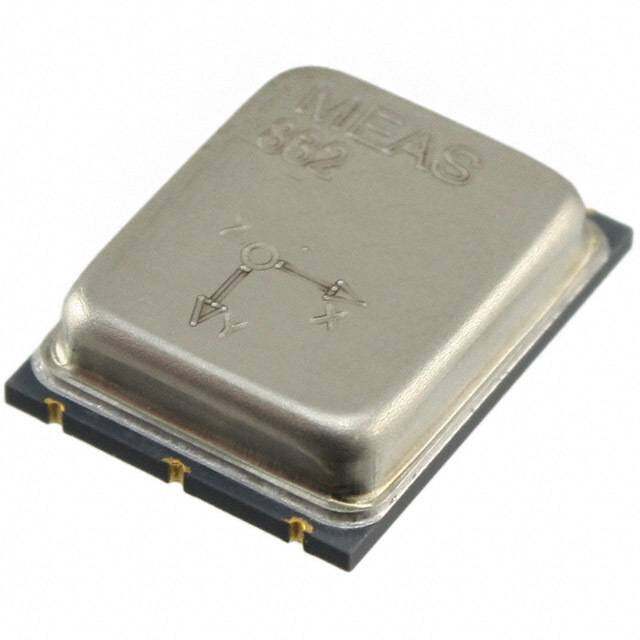
| 产品图片 |
|
| rohs | RoHS 合规性豁免无铅 / 符合限制有害物质指令(RoHS)规范要求 |
| 产品系列 | 加速计,Freescale Semiconductor MMA7660FCR1- |
| 数据手册 | |
| 产品型号 | MMA7660FCR1 |
| 产品种类 | 加速计 |
| 传感轴 | X, Y, Z |
| 供应商器件封装 | 10-DFN(3x3) |
| 其它名称 | MMA7660FCR1CT |
| 分辨率 | 6 bit |
| 加速 | 1.5 g |
| 加速度范围 | ±1.5g |
| 单位重量 | 20.100 mg |
| 商标 | Freescale Semiconductor |
| 安装类型 | 表面贴装 |
| 封装 | Reel |
| 封装/外壳 | 10-VFDFN |
| 封装/箱体 | DFN-10 |
| 工厂包装数量 | 1000 |
| 带宽 | - |
| 接口 | I2C |
| 数字输出-位数 | 6 bit |
| 数字输出-总线接口 | I2C |
| 最大工作温度 | + 85 C |
| 最小工作温度 | - 40 C |
| 标准包装 | 1 |
| 灵敏度 | 21.33 count/g |
| 特色产品 | http://www.digikey.com/cn/zh/ph/Freescale/mma7660.html |
| 电压-电源 | 2.4 V ~ 3.6 V |
| 系列 | MMA7660FC |
| 轴 | X,Y,Z |
| 输出类型 | Digital |


- 商务部:美国ITC正式对集成电路等产品启动337调查
- 曝三星4nm工艺存在良率问题 高通将骁龙8 Gen1或转产台积电
- 太阳诱电将投资9.5亿元在常州建新厂生产MLCC 预计2023年完工
- 英特尔发布欧洲新工厂建设计划 深化IDM 2.0 战略
- 台积电先进制程称霸业界 有大客户加持明年业绩稳了
- 达到5530亿美元!SIA预计今年全球半导体销售额将创下新高
- 英特尔拟将自动驾驶子公司Mobileye上市 估值或超500亿美元
- 三星加码芯片和SET,合并消费电子和移动部门,撤换高东真等 CEO
- 三星电子宣布重大人事变动 还合并消费电子和移动部门
- 海关总署:前11个月进口集成电路产品价值2.52万亿元 增长14.8%
PDF Datasheet 数据手册内容提取
Freescale Semiconductor Document Number: MMA7660FC Data Sheet: Technical Data Rev 8, 03/2012 An Energy Efficient Solution by Freescale 3-Axis Orientation/Motion Detection Sensor MMA7660FC The MMA7660FC is a ±1.5 g 3-Axis Accelerometer with Digital Output (I2C). It is a very low power, low profile capacitive MEMS sensor featuring a low pass filter, compensation for 0g offset and gain errors, and conversion to 6-bit digital values at a user configurable samples per second. The device can MMA7660FC: XYZ-AXIS be used for sensor data changes, product orientation, and gesture detection ACCELEROMETER through an interrupt pin (INT). The device is housed in a small 3mm x 3mm x ±1.5 g 0.9mm DFN package. Features • Digital Output (I2C) Bottom View • 3mm x 3mm x 0.9mm DFN Package • Low Power Current Consumption: Off Mode: 0.4 µA, Standby Mode: 2 µA, Active Mode: 47 µA at 1 ODR • Configurable Samples per Second from 1 to 120 samples a second. • Low Voltage Operation: – Analog Voltage: 2.4 V - 3.6 V – Digital Voltage: 1.71 V - 3.6 V • Auto-Wake/Sleep Feature for Low Power Consumption 10 LEAD • Tilt Orientation Detection for Portrait/Landscape Capability DFN CASE 2002-03 • Gesture Detection Including Shake Detection and Tap Detection • Robust Design, High Shocks Survivability (10,000 g) • RoHS Compliant Top View • Halogen Free • Environmentally Preferred Product • Low Cost RESERVED 1 10 RNE/CSERVED Typical Applications N/C 2 9 DVDD • Mobile Phone/ PMP/PDA: Orientation Detection (Portrait/Landscape), Image Stability, Text Scroll, Motion Dialing, Tap to Mute AVDD 3 8 DVSS • Laptop PC: Anti-Theft AVSS 4 7 SDA • Gaming: Motion Detection, Auto-Wake/Sleep For Low Power INT 5 6 SCL Consumption • Digital Still Camera: Image Stability Figure1. Pin Connections ORDERING INFORMATION Part Number Temperature Range Package Shipping MMA7660FCT –40 to +85°C DFN-10 Tray MMA7660FCR1 –40 to +85°C DFN-10 7” Tape & Reel © 2009-2012 Freescale Semiconductor, Inc. All rights reserved.
Contents DEFINITIONS ...............................................................................................................................................................................5 ELECTRO STATIC DISCHARGE (ESD) ......................................................................................................................................7 PRINCIPLE OF OPERATION ......................................................................................................................................................9 MODES OF OPERATION ..........................................................................................................................................................10 CONFIGURABLE SAMPLES PER SECONDS AND INTERRUPT SETTINGS .........................................................................11 POWER SAVING FEATURES ...................................................................................................................................................11 TESTING THE LOGIC CHAIN ...................................................................................................................................................11 FEATURES ................................................................................................................................................................................11 Tap Detection ......................................................................................................................................................................13 Shake Detection ..................................................................................................................................................................13 Auto-Wake/Sleep ................................................................................................................................................................13 REGISTER DEFINITIONS .........................................................................................................................................................14 SERIAL INTERFACE .................................................................................................................................................................22 Serial-Addressing ................................................................................................................................................................22 Start and Stop Conditions ...................................................................................................................................................22 Bit Transfer ..........................................................................................................................................................................22 Acknowledge .......................................................................................................................................................................23 The Slave Address ..............................................................................................................................................................23 Message Format for Writing MMA7660FC ..........................................................................................................................23 Message Format for Reading MMA7660FC ........................................................................................................................24 APPENDIX A - PACKAGE REQUIREMENTS FOR MMA7660FC .............................................................................................25 Minimum Recommended Footprint for Surface Mounted Applications ...............................................................................25 Soldering And Mounting Guidelines for the DFN Accelerometer Sensor to a PC Board ....................................................25 Overview of Soldering Considerations ................................................................................................................................25 Halogen Content .................................................................................................................................................................25 PCB Mounting Recommendations ......................................................................................................................................25 APPENDIX B - SENSING DIRECTION ......................................................................................................................................27 APPENDIX C - MMA7660FC ACQUISITION CODE TABLE .....................................................................................................28 APPENDIX D - I2C AC CHARACTERISTICS ............................................................................................................................30 MMA7660FC Sensors Freescale Semiconductor 2
List of Tables Pin Description . . . . . . . . . . . . . . . . . . . . . . . . . . . . . . . . . . . . . . . . . . . . . . . . . . . . . . . . . . . . . . . . . . . . . . . . . . . . . . . . . . . . . . .6 Maximum Ratings . . . . . . . . . . . . . . . . . . . . . . . . . . . . . . . . . . . . . . . . . . . . . . . . . . . . . . . . . . . . . . . . . . . . . . . . . . . . . . . . . . . . .7 ESD And Latch-up Protection Characteristics . . . . . . . . . . . . . . . . . . . . . . . . . . . . . . . . . . . . . . . . . . . . . . . . . . . . . . . . . . . . . . .7 Operating Characteristics . . . . . . . . . . . . . . . . . . . . . . . . . . . . . . . . . . . . . . . . . . . . . . . . . . . . . . . . . . . . . . . . . . . . . . . . . . . . . . .8 Modes Of Operation . . . . . . . . . . . . . . . . . . . . . . . . . . . . . . . . . . . . . . . . . . . . . . . . . . . . . . . . . . . . . . . . . . . . . . . . . . . . . . . . . .10 Feature Summary Table . . . . . . . . . . . . . . . . . . . . . . . . . . . . . . . . . . . . . . . . . . . . . . . . . . . . . . . . . . . . . . . . . . . . . . . . . . . . . . .11 Orientation Detection Logic of when Interrupt will Occur . . . . . . . . . . . . . . . . . . . . . . . . . . . . . . . . . . . . . . . . . . . . . . . . . . . . . .12 Auto-Wake/Sleep Truth Table . . . . . . . . . . . . . . . . . . . . . . . . . . . . . . . . . . . . . . . . . . . . . . . . . . . . . . . . . . . . . . . . . . . . . . . . . .13 User Register Summary . . . . . . . . . . . . . . . . . . . . . . . . . . . . . . . . . . . . . . . . . . . . . . . . . . . . . . . . . . . . . . . . . . . . . . . . . . . . . . .14 Modes . . . . . . . . . . . . . . . . . . . . . . . . . . . . . . . . . . . . . . . . . . . . . . . . . . . . . . . . . . . . . . . . . . . . . . . . . . . . . . . . . . . . . . . . . . . . .17 ASE/AWE Conditions . . . . . . . . . . . . . . . . . . . . . . . . . . . . . . . . . . . . . . . . . . . . . . . . . . . . . . . . . . . . . . . . . . . . . . . . . . . . . . . . .18 Sleep Counter Timeout Ranges . . . . . . . . . . . . . . . . . . . . . . . . . . . . . . . . . . . . . . . . . . . . . . . . . . . . . . . . . . . . . . . . . . . . . . . . .18 I2C AC Characteristics . . . . . . . . . . . . . . . . . . . . . . . . . . . . . . . . . . . . . . . . . . . . . . . . . . . . . . . . . . . . . . . . . . . . . . . . . . . . . . . .30 MMA7660FC Sensors Freescale Semiconductor 3
List of Figures I2C Connection to MCU . . . . . . . . . . . . . . . . . . . . . . . . . . . . . . . . . . . . . . . . . . . . . . . . . . . . . . . . . . . . . . . . . . . . . . . . . . . . . . . .6 Simplified Accelerometer Functional Block Diagram . . . . . . . . . . . . . . . . . . . . . . . . . . . . . . . . . . . . . . . . . . . . . . . . . . . . . . . . . .7 Simplified Transducer Physical Model . . . . . . . . . . . . . . . . . . . . . . . . . . . . . . . . . . . . . . . . . . . . . . . . . . . . . . . . . . . . . . . . . . . . .9 State Machine of Modes . . . . . . . . . . . . . . . . . . . . . . . . . . . . . . . . . . . . . . . . . . . . . . . . . . . . . . . . . . . . . . . . . . . . . . . . . . . . . . .10 Orientation Detection Logic in 3-Dimensional Space . . . . . . . . . . . . . . . . . . . . . . . . . . . . . . . . . . . . . . . . . . . . . . . . . . . . . . . . .12 2-Wire Serial Interface Timing Details . . . . . . . . . . . . . . . . . . . . . . . . . . . . . . . . . . . . . . . . . . . . . . . . . . . . . . . . . . . . . . . . . . . .22 Start and Stop Conditions . . . . . . . . . . . . . . . . . . . . . . . . . . . . . . . . . . . . . . . . . . . . . . . . . . . . . . . . . . . . . . . . . . . . . . . . . . . . . .22 Bit Transfer . . . . . . . . . . . . . . . . . . . . . . . . . . . . . . . . . . . . . . . . . . . . . . . . . . . . . . . . . . . . . . . . . . . . . . . . . . . . . . . . . . . . . . . . .22 Acknowledge . . . . . . . . . . . . . . . . . . . . . . . . . . . . . . . . . . . . . . . . . . . . . . . . . . . . . . . . . . . . . . . . . . . . . . . . . . . . . . . . . . . . . . .23 Slave Address . . . . . . . . . . . . . . . . . . . . . . . . . . . . . . . . . . . . . . . . . . . . . . . . . . . . . . . . . . . . . . . . . . . . . . . . . . . . . . . . . . . . . .23 Single Byte Write . . . . . . . . . . . . . . . . . . . . . . . . . . . . . . . . . . . . . . . . . . . . . . . . . . . . . . . . . . . . . . . . . . . . . . . . . . . . . . . . . . . .23 Multiple Bytes Write . . . . . . . . . . . . . . . . . . . . . . . . . . . . . . . . . . . . . . . . . . . . . . . . . . . . . . . . . . . . . . . . . . . . . . . . . . . . . . . . . .24 Single Byte Read . . . . . . . . . . . . . . . . . . . . . . . . . . . . . . . . . . . . . . . . . . . . . . . . . . . . . . . . . . . . . . . . . . . . . . . . . . . . . . . . . . . .24 Multiple Bytes Read . . . . . . . . . . . . . . . . . . . . . . . . . . . . . . . . . . . . . . . . . . . . . . . . . . . . . . . . . . . . . . . . . . . . . . . . . . . . . . . . . .24 Package Footprint, PCB Land Pattern, and Stencil Design . . . . . . . . . . . . . . . . . . . . . . . . . . . . . . . . . . . . . . . . . . . . . . . . . . . .26 PCB Land Pattern Detail . . . . . . . . . . . . . . . . . . . . . . . . . . . . . . . . . . . . . . . . . . . . . . . . . . . . . . . . . . . . . . . . . . . . . . . . . . . . . .26 Product Orientation on Perpendicular Axis . . . . . . . . . . . . . . . . . . . . . . . . . . . . . . . . . . . . . . . . . . . . . . . . . . . . . . . . . . . . . . . . .27 Product Orientations Showing Direction for Each Axis in Composite . . . . . . . . . . . . . . . . . . . . . . . . . . . . . . . . . . . . . . . . . . . . .27 MMA7660FC Sensors Freescale Semiconductor 4
Definitions Auto-Wake: Sleep Mode (uses AMSR sample rate in SR [0x08] register) Auto-Sleep: Run Mode (uses AWSR sample rate in SR [0x08] register) PMP: Portable Media Player PDA: Personal Digital Assistant DFN: Dual Flat No Lead ESD: Electro Static Discharge ODR: Output Data Rate MEMS: Microelectromechanical Systems MMA7660FC Sensors Freescale Semiconductor 5
Table1. Pin Description Top View Pin Pin # Pin Name Description Status 1 RESERVED Connect to AVSS Input RESERVED 1 10 RESERVED 2 N/C No Internal Connection, leave Input unconnected or connect to Ground N/C 2 9 DVDD 3 AVDD Device Power Input 4 AVSS Device Ground Input AVDD 3 8 DVSS 5 INT Interrupt/Data Ready Output AVSS 4 7 SDA 6 SCL I2C Serial Clock Input 7 SDA I2C Serial Data Open INT 5 6 SCL Drain 8 DVSS Digital I/O Ground Input 9 DVDD Digital I/O Power Input Figure1. Pinout 10 RESERVED Connect to AVSS Input VDD VDD U13 1 10 RESERVED RESERVED 2 9 N/C DVDD 3 8 AVDD DVSS 4 7 AVSS SDA 5 6 INT SCL GND GND VDD MMA7660FC R1 R2 4.70 K 4.70 K SDA MCU SCL INT NOTE: A 0.1 μF ceramic capacitor can be placed connecting pin 3 (AVDD) to pin 4 (AVSS). In addition, another 0.1 μF ceramic capacitor can be place connecting pin 9 (DVDD) to pin 8 (DVSS). The capacitors should be placed close to the pins of the MMA7660FC and is recommended for testing and to adequately decouple the accelerometer from noise on the power supply. Figure2. I2C Connection to MCU MMA7660FC Sensors Freescale Semiconductor, Inc. 6
AVDD DVDD INTERNAL CLOCK VSS OSC GEN X-axis Transducer TraYn-sadxuiscer MUX CONCV-tEoR-VTER AMP ADC I2C SDA SCL Z-axis Transducer OFFSET GAIN TRIM TRIM CONTROL LOGIC INT Figure3. Simplified Accelerometer Functional Block Diagram Table2. Maximum Ratings (Maximum ratings are the limits to which the device can be exposed without causing permanent damage.) Rating Symbol Value Unit Maximum Acceleration (all axes, 100 μs) g 10,000 g max Analog Supply Voltage AV -0.3 to +3.6 V DD Digital I/O pins Supply Voltage DV -0.3 to +3.6 V DD_IO Drop Test D 1.8 m drop Storage Temperature Range T -40 to +125 °C stg ELECTRO STATIC DISCHARGE (ESD) WARNING: This device is sensitive to electrostatic discharge. Although the Freescale accelerometer contains internal 2000 V ESD protection circuitry, extra precaution must be taken by the user to protect the chip from ESD. A charge of over 2000 V can accumulate on the human body or associated test equipment. A charge of this magnitude can alter the performance or cause failure of the chip. When handling the accelerometer, proper ESD precautions should be followed to avoid exposing the device to discharges which may be detrimental to its performance. Table3. ESD And Latch-up Protection Characteristics Rating Symbol Value Unit Human Body Model HBM ±2000 V Machine Model MM ±200 V Charge Device Model CDM ±500 V Latch-up current at T = 85°C ±100 mA A MMA7660FC Sensors 7 Freescale Semiconductor, Inc.
Table4. Operating Characteristics Unless otherwise noted: -40°C < T < 85°C, 2.4 V < AV < 3.6 V, 1.71 V < DV < 3.6 V, Acceleration = 0g A DD DD Typical values are at AV = 2.8 V, DV = 2.8 V, T = +25°C DD DD A Characteristics Symbol Min Typ Max Unit Analog Supply Voltage Standby/Operation Mode AV 2.4 2.8 3.6 V DD Enable Bus Modeon Mode AV 0 V DD Digital I/O Pins Supply Voltage Standby/Operation Mode DV 1.71 2.8 AV V DD_IO DD Enable Bus Modeon Mode DV 1.71 1.8 3.6 V DD_IO Supply Current Drain Off Mode I 0.4 µA DD Power Down Mode I 2 µA DD Standby Mode(1) I 0 2 10 µA DD Active Mode, ODR = 1 I 47 µA DD Active Mode, ODR = 2 I 49 µA DD Active Mode, ODR = 4 I 54 µA DD Active Mode, ODR = 8 I 66 µA DD Active Mode, ODR = 16 I 89 µA DD Active Mode, ODR = 32 I 133 µA DD Active Mode, ODR = 64 I 221 µA DD Active Mode(1), ODR = 120 I 294 µA DD Acceleration Range ±1.5 g Operating Temperature Range T -40 25 85 °C A 0g Output Signal (T = 25°C, AV = 2.8 V) A DD 0g Offset ±1.5g range(1) V -3 0 3 counts OFF 0g Offset Temperature Variation X -1.3 mg/°C Y +1.5 mg/°C Z -1.0 mg/°C Sensitivity(1) (T = 25°C, AV = 2.8 V) A DD ±1.5g range 6-bit 21.33 count/g Acceleration Sensitivity at T 19.62 21.33 23.04 count/g AMB Acceleration Sensitivity Temperature Variation ±0.01 %/°C Input High Voltage V 0.7 x D IH VDD Input Low Voltage V 0.35 x D IL VDD Output Low Voltage (IOL = 6 mA + SDA, INT) V 0.5 V OL Input Leakage Current I , I 0.025 µA IH IL Internal Clock Frequency(1) (TA = 25°C, AVDD = 2.8 V) tCLK 135 150 165 kHz I2C Interface Speed 400 kHz Control Timing Turn on time from AV = 0 V to AV = 2.5 V(2) 1.3 ms DD DD Turn off time from Active to Standby Mode 1 ms Turn on time Standby to Active Mode 12 ms + 1/ODR ms Timing Clock Source Accuracy (T = 25°C, DV = 1.8 V) -10 10 % A DD Timing Clock Source Temperature Variation -15 15 % Cross Axis Sensitivity(3) ±1 % Noise(4) ±1 count Notes 1.These parameters are tested in production at final test. 2.Assuming VDD power on slope is < 1 ms. 3.A measure of the devices ability to reject an acceleration applied 90° from the true axis of sensitivity. 4.Noise is defined as quantiles given to a sample size. These are the occurrences of noise: 94% = ±1 count, 5% = ±2 counts, and 1% = ±3 counts. MMA7660FC Sensors Freescale Semiconductor, Inc. 8
PRINCIPLE OF OPERATION The Freescale Accelerometer consists of a MEMS capacitive sensing g-cell and a signal conditioning ASIC contained in a single package. The sensing element is sealed hermetically at the wafer level using a bulk micro machined cap wafer. The g-cell is a mechanical structure formed from semiconductor materials (polysilicon) using masking and etching processes. The sensor can be modeled as a movable beam that moves between two mechanically fixed beams (Figure4). Two gaps are formed; one being between the movable beam and the first stationary beam and the second between the movable beam and the second stationary beam. The ASIC uses switched capacitor techniques to measure the g-cell capacitors and extract the acceleration data from the difference between the two capacitors. The ASIC also signal conditions and filters (switched capacitor) the signal, providing a digital output that is proportional to acceleration. ACCELERATION Figure4. Simplified Transducer Physical Model MMA7660FC Sensors 9 Freescale Semiconductor, Inc.
MODES OF OPERATION The sensor has three power modes: Off Mode, Standby Mode, and Active Mode to offer the customer different power consumption options. The sensor is only capable of running in one of these modes at a time. The Off Mode offers the lowest power consumption, approximately 0.4 µA and can only be reached by powering down the analog supply. See Figure5. In this mode, there is no analog supply and all I2C activity is ignored. The Standby Mode is ideal for battery operated products. When Standby Mode is active the device outputs are turned off providing a significant reduction in operating current. When the device is in Standby Mode the current will be reduced to approximately 3 µA. Standby Mode is entered as soon as both analog and digital power supplies are up. In this mode, the device can read and write to the registers with I2C, but no new measurements can be taken. The mode of the device is controlled through the MODE (0x07) control register by accessing the mode bit in the Mode register. During the Active Mode, continuous measurement on all three axes is enabled. In addition, the user can choose to enable: Shake Detection, Tap Detection, Orientation Detection, and/or Auto-Wake/Sleep Feature and in this mode the digital analysis for any of these functions is done. The user can configure the samples per second to any of the following: 1 sample/second, 2 samples/second, 4 samples/second, 8 samples/second, 16 samples/second, 32 samples/second, 64 samples/second, and 120 samples/second, for the Auto-Sleep state. If the user is configuring the Auto-Wake feature, the selectable ranges are: 1 sample/second, 8 samples/second, 16 samples/seconds and 32 samples/second. Depending on the samples per second selected the power consumption will vary. Table5. Modes Of Operation Measurement and I²C Bus DVDD AVDD Function Power Mode Power Down DVDD is down, so I2C bus cannot be Off Off MMA7660FC is powered down in both supplies. I2C activity is Mode used for other devices (MMA7660FC unavailable on bus. clamps I2C bus to DVVD pin) Off On MMA7660FC is powered down in digital supply but not analog supply. I2C activity is unavailable on bus. AVDD power cycling requires 50 msec. Off Mode MMA7660FC will not respond, but I2C On Off MMA7660FC is powered down in analog supply but not digital bus can be used for other devices supply. I2C activity is ignored. (MMA7660FC does not load I2C bus) Standby Mode MMA7660FC will respond to I2C bus On On MMA7660FC is powered up in both supplies, so registers can be accessed normally to set MMA7660FC to Active Mode when desired. MMA7660FC's sensor measurement system is idle. Active Mode MMA7660FC will respond to I2C bus On On MMA7660FC is able to operate sensor measurement system at Auto-Sleep user programmable samples per second and run all of the digital Auto-Wake analysis functions. Tap detection operates in Active Mode and Auto-Sleep, but not Auto-Wake. Figure5. State Machine of Modes MMA7660FC Sensors Freescale Semiconductor, Inc. 10
CONFIGURABLE SAMPLES PER SECONDS AND INTERRUPT SETTINGS The device can be configured into 8 different samples per seconds including: 1 sample/second, 2 samples/second, 4 samples/second, 8 samples/second, 16 samples/second, 32 samples/second, 64 samples/second, and 120 samples/second, The user can specify the samples per second for their particular application, deciding on the trade off between power consumption and number of samples, this can be configured in the SR (0x08) register. Once the user configurable samples per second is chosen, the device will update the data for all 3 axes in the register at a resolution of 6-bits/axis. The user can choose to enable/disable any of the following interrupts in the INTSU (0x06) register: Front/Back Interrupt, Up/Down/Left/Right Interrupt, Tap Detection Interrupt, GINT (real-time motion tracking), Shake on X-axis, Shake on Y-axis, and Shake on Z-axis. If the GINT is enabled, real-time motion tracking can be configured to trigger an interrupt after every sensor data update: 1s (1 sample/second), 500 ms (2 samples/second), 250 ms (4 samples/second), 125 ms (8 samples/second), 62.5 ms (16 samples/second), 31.25 ms (32 samples/second), 15.625 ms (64 samples/second), or 8.36 ms (120 samples/ second). If any of the shake axis interrupts are enabled; excessive agitation, greater than 1.3 g, will trigger an interrupt. If either the Up/Down/Left/Right Interrupt or the Front/Back Interrupt is enabled, any change in orientation will generate an interrupt. When the Auto-Wake feature is enabled, and the Auto-Sleep counter elapses an interrupt will occur. When the device is in Auto-Sleep state, if a shake interrupt, tap interrupt, Delta G, or orientation detection interrupt occur, the device will go out of sleep state and into wake state. POWER SAVING FEATURES The MMA7660FC includes a range of user configurable power saving features. The device’s samples per second can be set over a wide range from 1 to 120 samples a second; the operating current is directly proportional to samples per second. The analog supply A can be powered down to put the MMA7660FC into Off Mode, which typically draws 0.4 µA. The Auto-Wake/ VDD Sleep feature can toggle the sampling rate from a higher user selected samples per second to a lower user selected samples per second, changing based on if motion is detected or not. The user can choose to use any of the above options to configure the part and make it have the optimal power consumption level for the desired application. TESTING THE LOGIC CHAIN MMA7660FC can be put into Test Mode, which disables accelerometer measurements and instead allows the user to write 6-bit values directly to the three axis data registers, thus simulating real time accelerometer measurements. The state machine will respond to these values according to the enabled features and functions, allowing them to be validated. NOTE: MMA7660FC does not include an accelerometer self test function, which is typically an electrostatic force applied to each axis to cause it to deflect. FEATURES The Sensor employs both analog and digital filtering to ensure low noise and accurate output when using the part for Shake, Tap, or Orientation Detection. During Active Mode, the data is filtered and stored for each of the 3 axes at the specified following measurement intervals: 1s (1 sample/second), 500 ms (2 samples/second), 250 ms (4 samples/second), 125 ms (8 samples/second), 62.5 ms (16 samples/second), 31.25 ms (32 samples/second), 15.625 ms (64 samples/second), or 8.36 ms (120 samples/second) or indicated in AMSR [2:0]. The 6-bit measurement data is stored in the XOUT (0x00), YOUT (0x01), and ZOUT (0x02) registers and is used to update the Shake, Alert, Tap, PoLa[2:0] (updates Up, Down, Left, and Right position), and BaFro[1:0] (updates Back and Front position) in the TILT (0x03) register used for orientation detection. The customer can configure the part by enabling a number of user- desired interrupts in the INTSU (0x06) register. Once the interrupts are enabled a change in filtered readings will cause an interrupt to occur depending on the output. The filters that are being used by this sensor is the analog filtering, digital noise filtering of measurements used for orientation detection and updated in the XOUT (0x00), YOUT (0x01), and ZOUT (0x02) registers. The filtering method used is to oversample each axis by taking 32 readings, and then calculate the average for the output measurement data as a finite impulse response filter. Table6. Feature Summary Table Feature Will Generate Interrupt Orientation Change When FBINT, PLINT = 1 Shake When SHINTX, SHINTY, SHINTZ = 1 Tap or Tilt When PDINT = 1 Auto-Wake/Sleep When ASINT = 1 X, Y, Z Data Update When GINT = 1 NOTE: Sensor Measurements are NOT taken in Standby Mode or in Test Mode. MMA7660FC Sensors 11 Freescale Semiconductor, Inc.
Orientation Detection Orientation Detection Logic MMA7660FC gives the customer the capability to do orientation detection for such applications as Portrait/Landscape in Mobile Phone/PDA/ PMP. The tilt orientation of the device is in 3 dimensions and is identified in its last known static position. This enables a product to set its display orientation appropriately to either portrait/landscape mode, or to turn off the display if the product is placed upside down. The sensor provides six different positions including: Left, Right, Up, Down, Back, and Front, shown in Table7. In Active Mode the data is processed and updates the orientation positions in the TILT (0x03) register. At each measurement interval, it computes new values for Left, Right, Up, Down, Back, and Front but it does not automatically update these bits in the TILT (0x03) register. These values are updated depending on the debounce filter settings (SR Register 0x08) configured by the customer. In order to give the customer the ability to configure the debounce filter, specific to there application, they can change the following bits in the SR (0x08) register, FILT [2:0]. Please see below for a more detailed explanation of how the FILT [2:0] works in conjunction with updating the TILT (0x03) register: • If FILT [2:0] = 000, then the new values for Left, Right, Up, Down, Back, and Front are updated in the TILT (0x03) register (PoLa [2:0] and BaFro [1:0]) after every reading without any further analysis. • If FILT [2:0] = 001 – 111, then the sensor requires the computed values for Left, Right, Up, Down, Back, and Front to be the same from 1-7 consecutive readings (depending on the value in FILT [2:0], before updating the values stored in TILT (0x03) register (PoLa [2:0] and BaFro [1:0]). The debounce counter is reset after a mismatched reading or the TILT (0x03) register is updated (if the orientation condition is met). Table7. Orientation Detection Logic of when Interrupt will Occur Orientation Xg Yg Zg Shake |X| > +1.3g or |Y| > +1.3g or |Z| > +1.3g Up |Z| < 0.8g and |X| > |Y| and X < 0 Down |Z| < 0.8g and |X| > |Y| and X > 0 Right |Z| < 0.8g and |Y| > |X| and Y < 0 Left |Z| < 0.8g and |Y| > |X| and Y > 0 Back Z < -0.25g Front Z > 0.25g FFrroonntt UUpp LLeefftt RRiigghhtt DDoowwnn BBaacckk Figure6. Orientation Detection Logic in 3-Dimensional Space MMA7660FC Sensors Freescale Semiconductor, Inc. 12
Tap Detection The MMA7660FC also includes a Tap Detection feature that can be used for a number of different customer applications such as button replacement. For example, a single tap can stop a song from playing and a double tap can play a song. This function detects a fast transition that exceeds a user-defined threshold (PDET (0x09) register) for a set duration (PD (0x0A) register). Tap Detection Setup In order to enable Tap detection in the device the user must enable the Tap Interrupt in the INTSU (0x06) register and AMSR [2:0] = 000 in the SR (0x08) register. In this mode, TILT (0x03) register, XOUT (0x00), YOUT (0x01), and ZOUT (0x02) registers will update at the 120 samples/second. The user can configure Tap Detection to be detected on X and/or Y and/or Z axes. The customer can configure this by changing the XDA, YDA, and/or ZDA bit in the PDET (0x09) register. Detection for enabled axes is decided on an OR basis: If the PDINT bit is set in the INTSU (0x06) register, the device reports the first axis for which it detects a tap by the Tap bit in the TILT (0x03) register. When the Tap bit in the TILT (0x03) register is set, tap detection ceases, but the device will continue to process orientation detection data. Tap detection will resume when the TILT (0x03) register is read. NOTE: Delta G is available with any AMSR setting, when XDA = YDA = ZDA = 1 (PDET = 1). When the sampling rate is less than 120 samples/second, the device can not detect tapping, but can detect small tilt angles (30 º angle change) which can not be detected by orientation detection. Shake Detection The shake feature can be used as a button replacement to perform functions such as scrolling through images or web pages on a Mobile Phone/PMP/PDA. The customer can enable the shake interrupt on any of the 3 axes, by enabling the SHINTX, SHINTY, and/or SHINTZ in the INTSU (0x06) register. MMA7660FC detects shake by examining the current 6-bit measurement for each axis in XOUT, YOUT, and ZOUT. The axes that are tested for shake detection are the ones enabled by SHINTX, SHINTY, and/or SHINTZ. If a selected axis measures greater that 1.3 or less than -1.3 g, then a shake is detected for that axis and an interrupt occurs. All three axes are checked independently, but a common Shake bit in the TILT register is set when shake is detected in any one of the selected axes. Therefore when all three (SHINTX, SHINTY, and/or SHINTZ) are selected the sensor will not know what axis the shake occurred. When the TILT register is read the Shake bit is cleared during the acknowledge bit of the read access to that register and shake detection monitoring starts again. Auto-Wake/Sleep The MMA7660FC has the Auto-Wake/Sleep feature that can be enabled for power saving. In the Auto-Wake function, the device is put into a user specified low samples per second (1 sample/second, 8 samples/second, 16 samples/second, or 32 samples/second) in order to minimize power consumption. When the Auto-Wake is enabled and activity is detected such as a change in orientation, pulse event, Delta G acceleration or a shake event, then the device wakes up. Auto-Wake will automatically enable Auto-Sleep when the device is in wake mode and can therefore be configured to cause an interrupt on wake-up, by configuring the part to either wake-up with a change in orientation, shake, or if using the part at 120 samples/second tap detection. When the device is in Auto-Wake mode, the MODE (0x07) register, bit AWE is high. When the device has detected a change in orientation, a tap shake, or Delta G (change in acceleration), the device will enter Auto-Sleep mode. In the Auto- Sleep function, the device is put into any of the following user specified samples per seconds (1 sample/second, 2 samples/ second, 4 samples/second, 8 samples/second, 16 samples/second, 32 samples/second, 64 samples/second, and 120 samples/ second). In the Auto-Sleep mode, if no change in the orientation, shake or tap has occurred and the sleep counter has elapsed, the device will go into the Auto-Wake mode. When the device is in the Auto-Sleep mode, the MODE (0x07) register, bit ASE is high. The device can be programmed to continually cycle between Auto-Wake/Sleep. NOTE: The device can either be powered on in Wake/Sleep state depending on ASE/AWE settings. If the AWE bit is set, the device is powered on in, in sleep state. If the ASW bit is set, the device is powered on in, in wake state. Table8. Auto-Wake/Sleep Truth Table Trigger Wake-up Reset Sleep Counter Trigger Sleep Mode Orientation Detection Change Yes Yes No Shake Yes Yes No Delta G Yes Yes No (set with PD (0x0A) and PDET (0x09)) (XDA = YDA = ZDA = 0) Pulse Detect (120 samples/second) Yes Yes No Sleep Counter Elapsed No No Yes MMA7660FC Sensors 13 Freescale Semiconductor, Inc.
REGISTER DEFINITIONS Table9. User Register Summary Address Name Definition Bit 7 Bit 6 Bit 5 Bit 4 Bit 3 Bit 2 Bit 1 Bit 0 $00 XOUT 6-bit output value X - Alert XOUT[5] XOUT[4] XOUT[3] XOUT[2] XOUT[1] XOUT[0] $01 YOUT 6-bit output value Y - Alert YOUT[5] YOUT[4] YOUT[3] YOUT[2] YOUT[1] YOUT[0] $02 ZOUT 6-bit output value Z - Alert ZOUT[5] ZOUT[4] ZOUT[3] ZOUT[2] ZOUT[1] ZOUT[0] $03 TILT Tilt Status Shake Alert Tap PoLa[2] PoLa[1] PoLa[0] BaFro[1] BaFro[0] $04 SRST Sampling Rate Status 0 0 0 0 0 0 AWSRS AMSRS $05 SPCNT Sleep Count SC[7] SC[6] SC[5] SC[4] SC[3] SC[2] SC[1] SC[0] $06 INTSU Interrupt Setup SHINTX SHINTY SHINTZ GINT ASINT PDINT PLINT FBINT $07 MODE Mode IAH IPP SCPS ASE AWE TON - MODE $08 SR Auto-Wake/Sleep and FILT[2] FILT[1] FILT[0] AWSR[1] AWSR[0] AMSR[2] AMSR[1] AMSR[0] Portrait/Landscape samples per seconds and Debounce Filter $09 PDET Tap Detection ZDA YDA XDA PDTH[4] PDTH[3] PDTH[2] PDTH[1] PDTH[0] $0A PD Tap Debounce Count PD[7] PD[6] PD[5] PD[4] PD[3] PD[2] PD[1] PD[0] $0B-$1F Factory Reserved - - - - - - - - NOTE: To write to the registers the MODE bit in the MODE (0x07) register must be set to 0, placing the device in Standby Mode. $00: 6-bits output value X (Read Only when not in Test Mode) XOUT — X Output D7 D6 D5 D4 D3 D2 D1 D0 - Alert XOUT[5] XOUT[4] XOUT[3] XOUT[2] XOUT[1] XOUT[0] 0 0 0 0 0 0 0 0 Signed byte 6-bit 2’s complement data with allowable range of +31 to -32. XOUT[5] is 0 if the g direction is positive, 1 if the g direction is negative. If the Alert bit is set, the register was read at the same time as the device was attempting to update the contents. The register must be read again. $01: 6-bits output value Y (Read Only when not in Test Mode) YOUT — Y Output D7 D6 D5 D4 D3 D2 D1 D0 - Alert YOUT[5] YOUT[4] YOUT[3] YOUT[2] YOUT[1] YOUT[0] 0 0 0 0 0 0 0 0 Signed byte 6-bit 2’s complement data with allowable range of +31 to -32. YOUT[5] is 0 if the g direction is positive, 1 if the g direction is negative. If the Alert bit is set, the register was read at the same time as the device was attempting to update the contents. The register must be read again. $02: 6-bits output value Z (Read Only when not in Test Mode) ZOUT — Z Output D7 D6 D5 D4 D3 D2 D1 D0 - Alert ZOUT[5] ZXOUT[4] ZOUT[3] ZOUT[2] ZOUT[1] ZOUT[0] 0 0 0 0 0 0 0 0 Signed byte 6-bit 2’s complement data with allowable range of +31 to -32. ZOUT[5] is 0 if the g direction is positive, 1 if the g direction is negative. If the Alert bit is set, the register was read at the same time as the device was attempting to update the contents. The register must be read again. MMA7660FC Sensors Freescale Semiconductor, Inc. 14
$03: Tilt Status (Read only) TILT D7 D6 D5 D4 D3 D2 D1 D0 Shake Alert Tap PoLa[2] PoLa[1] PoLa[0] BaFro[1] BaFro[0] 0 0 0 0 0 0 0 0 BaFro[1:0] Tap 00:Unknown condition of front or back 1: Equipment has detected a tap 01: Front: Equipment is lying on its front 0: Equipment has not detected a tap 10: Back: Equipment is lying on its back Alert PoLa[2:0] 0: Register data is valid 000: Unknown condition of up or down or left or right 1: The register was read at the same time as MMA7660FC 001: Left: Equipment is in landscape mode to the left was attempting to update the contents. Re-read the register 010: Right: Equipment is in landscape mode to the right Shake 101: Down: Equipment standing vertically in inverted 0: Equipment is not experiencing shake in one or more of the orientation axes enabled by SHINTX, SHINTY, and SHINTZ 110: Up: Equipment standing vertically in normal orientation 1: Equipment is experiencing shake in one or more of the axes enabled by SHINTX, SHINTY, and SHINTZ Note: When entering active mode from standby mode, if the device is flat (±1g on Z-axis) the value for BaFro will be back (-1g) or front (+1g) but PoLa will be in unknown condition. if the device is being held in an Up/Down/Right/Left position, the PoLa value will be updated with current orientation, but BaFro will be in unknown condition. $04: Sample Rate Status Register (Read only) SRST D7 D6 D5 D4 D3 D2 D1 D0 0 0 0 0 0 0 AWSRS AMSRS 0 0 0 0 0 0 0 0 AMSRS AWSRS 0: Samples per second specified in AMSR[2:0] is not active 0: Samples per second specified in AWSR[1:0] is not active 1: Samples per second specified in AMSR[2:0] is active 1: Samples per second specified in AWSR[1:0] is active $05: Sleep Count Register (Read/Write) SPCNT D7 D6 D5 D4 D3 D2 D1 D0 SC[7] SC[6] SC[5] SC[4] SC[3] SC[2] SC[1] SC[0] 0 0 0 0 0 0 0 0 Writing to the SPCNT (0x05) register resets the internal sleep counter. SC[7:0] Sets the 8-bit maximum count value for the 8-bit internal sleep counter in Auto-Sleep. When the 8-bit internal sleep counter reaches the value set by SC[7:0], MMA7660FC will exit Auto-Sleep and switch to the samples per second specified in AWSR[1:0] of the SR (0x08) register. MMA7660FC Sensors 15 Freescale Semiconductor, Inc.
$06: Interrupt Setup Register INTSU D7 D6 D5 D4 D3 D2 D1 D0 SHINTX SHINTY SHINTZ GINT ASINT PDINT PLINT FBINT 0 0 0 0 0 0 0 0 FBINT SHINTX 0: Front/Back position change does not cause an interrupt 0: Shake on the X-axis does not cause an interrupt or set the 1: Front/Back position change causes an interrupt Shake bit in the TILT register PLINT 1: Shake detected on the X-axis causes an interrupt, and sets the Shake bit in the TILT register 0: Up/Down/Right/Left position change does not cause an interrupt SHINTY 1: Up/Down/Right/Left position change causes an interrupt 0: Shake on the Y-axis does not cause an interrupt or set the PDINT Shake bit in the TILT register 1: Shake detected on the Y-axis causes an interrupt, and sets 0: Successful tap detection does not cause an interrupt the Shake bit in the TILT register 1: Successful tap detection causes an interrupt SHINTZ ASINT 0: Shake on the Z-axis does not cause an interrupt or set the 0: Exiting Auto-Sleep does not cause an interrupt Shake bit in the TILT register 1: Exiting Auto-Sleep causes an interrupt 1: Shake detected on the Z-axis causes an interrupt, and sets GINT the Shake bit in the TILT register. 0: There is not an automatic interrupt after every measurement 1: There is an automatic interrupt after every measurement, when g-cell readings are updated in XOUT, YOUT, ZOUT registers, regardless of whether the readings have changed or not. This interrupt does not affect the Auto-Sleep or Auto- Wake functions. The active interrupt condition (IRQ = 0 if IAH = 0, IRQ = 1 if IAH = 1) is released during the acknowledge bit of the slave address transmission of the first subsequent I2C to MMA7660FC after the interrupt was asserted. MMA7660FC Sensors Freescale Semiconductor, Inc. 16
$07: Mode Register (Read/Write) MODE D7 D6 D5 D4 D3 D2 D1 D0 IAH IPP SCPS ASE AWE TON - MODE 0 0 0 0 0 0 0 0 NOTE: Writing to the Mode register resets sleep timing, and clears the XOUT, YOUT, ZOUT, TILT registers.Reading to the Mode register resets sleep timing. NOTE: The device must be placed in Standby Mode to change the value of the registers. Table10. Modes Mode of Operation D0 - MODE D2 - TON Standby Mode 0 0 Test Mode 0 1 Active Mode 1 0 NOTE: The device can only enter into Test Mode, when the previous mode was Standby Mode. If the device was in Active mode, set MMA766FC to Standby Mode (MODE = TON = 0), then enter Test Mode (MODE = 0, TON = 1). MODE ASE 0: Standby mode or Test Mode depending on state of TON 0: Auto-Sleep is disabled 1: Active mode 1: Auto-Sleep is enabled Existing state of TON bit must be 0, to write MODE = 1. Test When Auto-Sleep functionality is operating, the AMSRS bit is Mode must not be enabled. the SRST register is set and the device uses the samples per MMA7660FC always enters Active Mode using the samples second specified in AMSR[2:0] of the SR (0x08) register. per second specified in AMSR[2:0] of the SR (0x08) register. When MMA7660FC automatically exits Auto-Sleep because When MMA7660FC enters Active Mode with the Sleep Counter times out, the device will then switch to the [ASE:AWE]=11, MMA7660FC operates Auto-Sleep samples per second specified in AWSR[1:0] of the SR functionality first. register. If AWE = 1, then Auto-Wake functionality is now enabled (Table11). TON SCPS 0: Standby Mode or Active Mode depending on state of MODE 0: The prescaler is divide-by-1. The 8-bit internal Sleep 1: Test Mode Counter input clock is the samples per second set by Existing state of MODE bit must be 0, to write TON = 1. AMSR[2:0], so the clock range is 120 Hz to 1 Hz depending Device must be in Standby Mode. on AMSR[2:0] setting. Sleep Counter timeout range is In Test Mode (TON = 1), the data in the XOUT, YOUT and 256 times the prescaled clock (see Table12). ZOUT registers is not updated by measurement, but is 1: Prescaler is divide-by-16. The 8-bit Sleep Counter input instead updated by the user through the I2C interface for test clock is the samples per second set by AMSR[2:0] divided by purposes. Changes to the XOUT, YOUT and ZOUT register 16, so the clock range is 4 Hz to 0.0625 Hz depending on data is processed by MMA7660FC to change orientation AMSR[2:0] setting. Sleep Counter timeout range is 256 times status and generate interrupts just like Active Mode. the prescaled clock (see Table12). Debounce filtering and shake detection are disabled in Test IPP Mode. 0: Interrupt output INT is open-drain. AWE 1: Interrupt output INT is push-pull 0: Auto-Wake is disabled NOTE: Do NOT connect pull-up resistor from INT to 1: Auto-Wake is enabled. higher voltage than DVDD. When Auto-Wake functionality is operating, the AWSRS bit is IAH the SRST register is set and the device uses the samples per 0: Interrupt output INT is active low second specified in AWSR[1:0] of the SR (0x08) register. 1: Interrupt output INT is active high When MMA7660FC automatically exits Auto-Wake by a selected interrupt, the device will then switch to the samples per second specified in AMSR[2:0] of the SR (0x08) register. If ASE = 1, then Auto-Sleep functionality is now enabled (Table11). The active interrupt condition (IRQ = 0 if IAH = 0, IRQ = 1 if IAH = 1) is released during the acknowledge bit of the slave address transmission of the first subsequent I2C to the device after the interrupt was asserted. MMA7660FC Sensors 17 Freescale Semiconductor, Inc.
Table11. ASE/AWE Conditions Condition Auto-Wake (Sleep Mode) Auto-Sleep (Run Mode) AWE = 0, ASE = 0 X AWE = 1, ASE = 0 X AWE = 0, ASE = 1 X X AWE = 1, ASE = 1 X X NOTE: If interrupts are enabled, interrupts will behave normally in all conditions stated in Table11. Table12. Sleep Counter Timeout Ranges SCPS = 0 SCPS = 1 AMSR Minimum Range (20) Maximum Range (28) Minimum Range (20) Maximum Range (28) 1 SPS 1 s 256 s 16 s 4096 s 2 SPS 0.5 s 128 s 8 s 2048 s 4 SPS 0.25 s 34 s 4 s 1024 s 8 SPS 0.125 s 32 s 2 s 512 s 16 SPS 0.625 s 16 s 1 s 256 s 32 SPS 0.03125 s 8 s 0.5 s 128 s 64 SPS 0.0156 s 4 s 0.25 s 64 s 120 SPS 0.00836 s 2.14 s 0.133 s 34.24 s $08: Auto-Wake and Active Mode Portrait/Landscape Samples per Seconds Register (Read/Write) SR — Sample Rate Register D7 D6 D5 D4 D3 D2 D1 D0 FILT[2] FILT[1] FILT[0] AWSR[1] AWSR[0] AMSR[2] AMSR[1] AMSR[0] 0 0 0 0 0 0 0 0 MMA7660FC Sensors Freescale Semiconductor, Inc. 18
AMSR[2:0] NAME DESCRIPTION 000 AMPD Tap Detection Mode and 120 Samples/Second Active and Auto-Sleep Mode Tap Detection Sampling Rate: The device takes readings continually at a rate of nominally 3846 g-cell measurements a second. It then filters these high speed measurements by maintaining continuous rolling averages of the current and last g-cell measurements. The averages are updated every 260 µs to track fast moving accelerations. Tap detection: itself compares the two filtered axis responses (fast and slow) described above for each axis. The absolute (unsigned) difference between the fast and slow axis responses is compared against the tap detection delta threshold value PDTH[4:0] in the PDET (0x09) register. For portrait/landscape detection: The device takes and averages 32 g-cell measurements every 8.36 ms in Active Mode and Auto-Sleep. The update rate is 120 samples per second. These measurements update the XOUT (0x00), YOUT (0x01), and ZOUT (0x02) registers also. 001 AM64 64 Samples/Second Active and Auto-Sleep Mode For portrait/landscape detection: The device takes and averages 32 g-cell measurements every 15.625 ms in Active Mode and Auto-Sleep. The update rate is 64 samples per second. These measurements update the XOUT (0x00), YOUT (0x01), and ZOUT (0x02) registers also. 010 AM32 32 Samples/Second Active and Auto-Sleep Mode For portrait/landscape detection: The device takes and averages 32 g-cell measurements every 31.25 ms in Active Mode and Auto-Sleep. The update rate is 32 samples per second. These measurements update XOUT (0x00), YOUT (0x01), and ZOUT (0x02) registers also. 011 AM16 16 Samples/Second Active and Auto-Sleep Mode For portrait/landscape detection: The device takes and averages 32 g-cell measurements every 62.5 ms in Active Mode and Auto-Sleep. The update rate is 16 samples per second. These measurements update the XOUT (0x00), YOUT (0x01), and ZOUT (0x02) registers also. 100 AM8 8 Samples/Second Active and Auto-Sleep Mode For portrait/landscape detection: The device takes and averages 32 g-cell measurements every 125 ms in Active Mode and Auto-Sleep. The update rate is 8 samples per second. These measurements update the XOUT (0x00), YOUT (0x01), and ZOUT (0x02) registers also. 101 AM4 4 Samples/Second Active and Auto-Sleep Mode For portrait/landscape detection: The device takes and averages 32 g-cell measurements every 250 ms in Active Mode and Auto-Sleep. The update rate is 4 samples per second. These measurements update the XOUT (0x00), YOUT (0x01), and ZOUT (0x02) registers also. 110 AM2 2 Samples/Second Active and Auto-Sleep Mode For portrait/landscape detection: The device takes and averages 32 g-cell measurements every 500 ms in Active Mode and Auto-Sleep. The update rate is 2 samples per second. These measurements update the XOUT (0x00), YOUT (0x01), and ZOUT (0x02) registers also. 111 AM1 1 Sample/Second Active and Auto-Sleep Mode For portrait/landscape detection: The device takes and averages 32 g-cell measurements every 1000 ms in Active Mode and Auto-Sleep. The update rate is 1 sample per second. These measurements update the XOUT (0x00), YOUT (0x01), and ZOUT (0x02) registers also. MMA7660FC Sensors 19 Freescale Semiconductor, Inc.
AWSR[1:0] NAME DESCRIPTION 00 AW32 32 Samples/Second Auto-Wake Mode For portrait/landscape detection: The device takes and averages 32 g-cell measurements every 31.25 ms in Auto-Wake. The update rate is 32 samples per second. These measurements update the XOUT (0x00), YOUT (0x01), and ZOUT (0x02) registers also. 01 AW16 16 Samples/Second Auto-Wake Mode For portrait/landscape detection: The device takes and averages 32 g-cell measurements every 62.5 ms in Auto-Wake. The update rate is 16 samples per second. These measurements update the XOUT (0x00), YOUT (0x01), and ZOUT (0x02) registers also. 10 AW8 8 Samples/Second Auto-Wake Mode For portrait/landscape detection: The device takes and averages 32 g-cell measurements every 125 ms in Auto-Wake. The update rate is 8 samples per second. These measurements update the XOUT (0x00), YOUT (0x01), and ZOUT (0x02) registers also. 11 AW1 1 Sample/Second Auto-Wake Mode For portrait/landscape detection: The device takes and averages 32 g-cell measurements every 1000 ms in Auto-Wake. The update rate is 1 sample per second. These measurements update the XOUT (0x00), YOUT (0x01), and ZOUT (0x02) registers also. FILT[2:0] DESCRIPTION 000 Tilt debounce filtering is disabled. The device updates portrait/landscape every reading at the rate set by AMSR[2:0] or AWSR[1:0] 001 2 measurement samples at the rate set by AMSR[2:0] or AWSR[1:0] have to match before the device updates portrait/ landscape data in TILT (0x03) register. 010 3 measurement samples at the rate set by AMSR[2:0] or AWSR[1:0] have to match before the device updates portrait/ landscape data in TILT (0x03) register. 011 4 measurement samples at the rate set by AMSR[2:0] or AWSR[1:0] have to match before the device updates portrait/ landscape data in TILT (0x03) register. 100 5 measurement samples at the rate set by AMSR[2:0] or AWSR[1:0] have to match before the device updates portrait/ landscape data in TILT (0x03) register. 101 6 measurement samples at the rate set by AMSR[2:0] or AWSR[1:0] have to match before the device updates portrait/ landscape data in TILT (0x03) register. 110 7 measurement samples at the rate set by AMSR[2:0] or AWSR[1:0] have to match before the device updates portrait/ landscape data in TILT (0x03) register. 111 8 measurement samples at the rate set by AMSR[2:0] or AWSR[1:0] have to match before the device updates portrait/ landscape data in TILT (0x03) register. MMA7660FC Sensors Freescale Semiconductor, Inc. 20
$09: Tap/Pulse Detection Register (Read/Write) PDET D7 D6 D5 D4 D3 D2 D1 D0 ZDA YDA XDA PDTH[4] PDTH[3] PDTH[2] PDTH[1] PDTH[0] 0 0 0 0 0 0 0 0 NOTE: If XDA = YDA = ZDA = 0, samples per second is 120 samples/second, and Auto-Wake/Sleep feature is enabled, the tap interrupt will reset the sleep counter. PDTH[4:0] DESCRIPTION 00000 Tap detection threshold is ±1 count 00001 00010 Tap detection threshold is ±2 counts 00011 Tap detection threshold is ±3 counts ... ... and so on up to... 11101 Tap detection threshold is ±29 counts 11110 Tap detection threshold is ±30 counts 11111 Tap detection threshold is ±31 counts XDA ZDA 1: X-axis is disabled for tap detection 1: Z-axis is disabled for tap detection 0: X-axis is enabled for tap detection 0: Z-axis is enabled for tap detection YDA 1: Y-axis is disabled for tap detection 0: Y-axis is enabled for tap detection $0A: PD: Tap/Pulse Debounce Count Register (Read/Write) D7 D6 D5 D4 D3 D2 D1 D0 PD[7] PD[6] PD[5] PD[4] PD[3] PD[2] PD[1] PD[0] 0 0 0 0 0 0 0 0 PD[4:0] DESCRIPTION 00000000 The tap detection debounce filtering requires 2 adjacent tap detection tests to be the same to trigger a tap event and set the Tap bit in the TILT (0x03) register, and optionally set an interrupt if PDINT is set in the INTSU (0x06) register. Tap detection 00000001 response time is nominally 0.52 ms. 00000010 Tap detection debounce filtering requires 3 adjacent tap detection tests to be the same to trigger a tap event and set the Tap bit in the TILT (0x03) register, and optionally set an interrupt if PDINT is set in the INTSU (0x06) register. Tap detection response time is nominally 0.78 ms. 00000011 Tap detection debounce filtering requires 4 adjacent tap detection tests to be the same to trigger a tap event and set the Tap bit in the TILT (0x03) register, and optionally set an interrupt if PDINT is set in the INTSU (0x06) register. Tap detection response time is nominally 1.04 ms. ... ... and so on up to... 11111101 Tap detection debounce filtering requires 254 adjacent tap detection tests to be the same to trigger a tap event and set the Tap bit in the TILT (0x03) register, and optionally set an interrupt if PDINT is set in the INTSU (0x06) register. Tap detection response time is nominally 66.04 ms. 11111110 Tap detection debounce filtering requires 255 adjacent tap detection tests to be the same to trigger a tap event and set the Tap bit in the TILT (0x03) register, and optionally set an interrupt if PDINT is set in the INTSU (0x06) register. Tap detection response time is nominally 66.3 ms. 11111111 Tap detection debounce filtering requires 256 adjacent tap detection tests to be the same to trigger a tap event and set the Tap bit in the TILT (0x03) register, and optionally set an interrupt if PDINT is set in the INTSU (0x06) register. Tap detection response time is nominally 66.56 ms. MMA7660FC Sensors 21 Freescale Semiconductor, Inc.
SERIAL INTERFACE Serial-Addressing MMA7660FC operates as a slave that sends and receives data through an I2C 2-wire interface. The interface uses a Serial Data Line (SDA) and a Serial Clock Line (SCL) to achieve bi-directional communication between master(s) and slave(s). A master (typically a microcontroller) initiates all data transfers to and from the device, and generates the SCL clock that synchronizes the data transfer. SDA t BUF t t SUDAT SUSTA t tHDDAT HDSTA tSUSTO t LOW SCL t HIGH t HDSTA t t R F START REPEATEDSTART STOP START CONDITION CONDITION CONDITION CONDITION Figure7. 2-Wire Serial Interface Timing Details The device’s SDA line operates as both an input and an open-drain output. A pull-up resistor, typically 4.7 kΩ, is required on SDA. The device’s SCL line operates only as an input. A pull-up resistor, typically 4.7 kΩ, is required on SCL if there are multiple masters on the 2-wire interface, or if the master in a single-master system has an open-drain SCL output. Each transmission consists of a START condition (Figure7) sent by a master, followed by MMA7660FC's 7-bit slave address plus R/W bit, a register address byte, one or more data bytes, and finally a STOP condition. SDA SCL DATALINESTABLE DATAVALID CHANGEOF DATAALLOWED Figure8. Start and Stop Conditions Start and Stop Conditions Both SCL and SDA remain high when the interface is not busy. A master signals the beginning of a transmission with a START (S) condition by transitioning SDA from high to low while SCL is high. When the master has finished communicating with the slave, it issues a STOP (P) condition by transitioning SDA from low to high while SCL is high. The bus is then free for another transmission. Bit Transfer One data bit is transferred during each clock tap. See Figure9. The data on SDA must remain stable while SCL is high. SDA SCL S P START STOP CONDITION CONDITION Figure9. Bit Transfer MMA7660FC Sensors Freescale Semiconductor, Inc. 22
Acknowledge The acknowledge bit is a clocked 9th bit, shown in Figure10, which the recipient uses to handshake a receipt of each byte of data. Thus each byte transferred effectively requires 9-bits. The master generates the 9th clock tap, and the recipient pulls down SDA during the acknowledge clock tap, such that the SDA line is stable low during the high period of the clock tap. When the master is transmitting to MMA7660FC, it generates the acknowledge bit because it is the recipient. When the device is transmitting to the master, the master generates the acknowledge bit because the master is the recipient. START CLCOLCOKCPKU TLASPE FFOORR CONDITION ACKNOWLEDGEMENT SCL 1 2 8 9 SDA BYTRANSMITTER S SDA BYRECEIVER Figure10. Acknowledge The Slave Address MMA7660FC has a 7-bit long slave address, shown in Figure11. The bit following the 7-bit slave address (bit eight) is the R/W bit, which is low for a write command and high for a read command. The device has a factory set I2C slave address which is normally 1001100 (0x4C). Contact the factory to request a different I2C slave address, which is available in the range 0001000 to 1110111 (0x08 to 0xEF), by metal mask option. SDA 1 0 0 1 1 0 0 R/W ACK MSB SCL Figure11. Slave Address The device monitors the bus continuously, waiting for a START condition followed by its slave address. When the device recognizes its slave address, it acknowledges and is then ready for continued communication. Message Format for Writing MMA7660FC A write to MMA7660FC comprises the transmission of the device’s keyscan slave address with the R/W bit set to 0, followed by at least one byte of information. The first byte of information is the register address of the first internal register that is to be updated. The Master Write address is 1001 1000 (0x98). If a STOP condition is detected after just the register address is received, then MMA7660FC takes no action. See Figure12. MMA7660FC clears its internal register address pointer to register 0x00 when a STOP condition is detected, so a single byte write has no net effect because the register address given in this first and only byte is replaced by 0x00 at the STOP condition. The internal register address pointer is not, however, cleared on a repeated start condition. Use a single byte write followed by a repeated start to read back data from a register. Any bytes received after the register address are data bytes. The first data byte goes into the internal register of the device selected by the register address. See Figure12. Master ST Device Address [6:0] W Register Address [6:0] Data [7:0] SP Slave AK AK AK Figure12. Single Byte Write MMA7660FC Sensors 23 Freescale Semiconductor, Inc.
If multiple data bytes are transmitted before a STOP condition is detected, these bytes are generally stored in subsequent MMA7660FC internal registers because the register address generally auto-increments. Master ST Device Address [6:0] W Register Address [6:0] Data [7:0] Data [7:0] SP Slave AK AK AK AK Figure13. Multiple Bytes Write Message Format for Reading MMA7660FC MMA7660FC is read using it’s internally stored register address as address pointer, the same way the stored register address is used as address pointer for a write. The pointer generally auto-increments after each data byte is read using the same rules as for a write. Thus, a read is initiated by first configuring the device’s register address by performing a write (Figure12) followed by a repeated start. The Master Write address is 1001 1001 (0x99). The master can now read 'n' consecutive bytes from it, with the first data byte being read from the register addressed by the initialized register address. Master ST Device Address [6:0] W Register Address [6:0] SR Device Address [6:0] R NAK SP Slave AK AK AK Data [7:0] Figure14. Single Byte Read Master ST Device Address [6:0] W Register Address [6:0] SR Device Address [6:0] R AK Slave AK AK AK Data [7:0] Master AK AK NAK SP Slave Data [7:0] Data [7:0] Data [7:0] Figure15. Multiple Bytes Read MMA7660FC Sensors Freescale Semiconductor, Inc. 24
APPENDIX A – PACKAGE REQUIREMENTS FOR MMA7660FC Minimum Recommended Footprint for Surface Mounted Applications Surface mount board layout is a critical portion of the total design. The footprint for the surface mount packages must be the correct size to ensure proper solder connection interface between the board and the package. With the correct footprint, the packages will self-align when subjected to a solder reflow process. It is always recommended to design boards with a solder mask layer to avoid bridging and shorting between solder pads. Soldering And Mounting Guidelines for the DFN Accelerometer Sensor to a PC Board These guidelines are for soldering and mounting the Dual Flat No-Lead (DFN) package inertial sensors to printed circuit boards (PCBs). The purpose is to minimize the stress on the package after board mounting. The MMA7660 digital output accelerometer uses the DFN package platform. This section describes suggested methods of soldering these devices to the PC board for consumer applications. Pages 31, 32, and 33 show the package outline drawing for the package. Overview of Soldering Considerations Information provided here is based on experiments executed on DFN devices. They do not represent exact conditions present at a customer site. Hence, information herein should be used as guidance only and process and design optimizations are recommended to develop an application specific solution. It should be noted that with the proper PCB footprint and solder stencil designs the package will self-align during the solder reflow process. The following are the recommended guidelines to follow for mounting DFN sensors for consumer applications. Halogen Content This package is designed to be Halogen Free, exceeding most industry and customer standards. Halogen Free means that no homogeneous material within the assembly package shall contain chlorine (Cl) in excess of 700 ppm or 0.07% weight/weight or bromine (Br) in excess of 900 ppm or 0.09% weight/weight. Note: Halogen Free is only compliant to the MMA7660FC, not to the packaging material. PCB Mounting Recommendations 1. The PCB land should be designed with Non Solder Mask Defined (NSMD) as shown in Figure16 and Figure17. 2. No additional via pattern underneath package. 3. PCB land pad is 0.825 mm x 0.3 mm as shown in Figure16 and Figure17. 4. Do not solder down smaller side tabs on either end of the package. 5. The solder mask opening is equal to the size of the PCB land pad plus 0.15 mm. 6. The stencil aperture size is equal to the PCB land pad – minus 0.03 mm total. 7. Stencil thickness should be 75 μm. 8. Do not place any components or vias at a distance less than 2 mm from the package land area. This may cause additional package stress if it is too close to the package land area. 9. Signal traces connected to pads should be as symmetric as possible. Put dummy traces on NC pads in order to have same length of exposed trace for all pads. Signal traces with 0.15 mm width and minimum 0.5 mm length for all PCB land pads near the package are recommended as shown in Figure16 and Figure17. Wider trace can be continued after the 0.5 mm zone. 10. Use a standard pick and place process and equipment. Do not use a hand soldering process. 11. It is recommended to use a no clean solder paste. 12. Do not use a screw down or stacking to fix the PCB into an enclosure because this could bend the PCB putting stress on the package. 13. The PCB should be rated for the multiple lead-free reflow condition with max 260°C temperature. 14. No copper traces on top layer of PCB under the package. This will cause planarity issues with board mount. Freescale DFN sensors are compliant with Restrictions on Hazardous Substances (RoHS), having halide free molding compound (green) and lead-free terminations. These terminations are compatible with tin-lead (Sn-Pb) as well as tin-silver- copper (Sn-Ag-Cu) solder paste soldering processes. Reflow profiles applicable to those processes can be used successfully for soldering the devices. MMA7660FC Sensors 25 Freescale Semiconductor, Inc.
Figure16. Package Footprint, PCB Land Pattern, and Stencil Design Figure17. PCB Land Pattern Detail MMA7660FC Sensors Freescale Semiconductor, Inc. 26
APPENDIX B - SENSING DIRECTION Top View Direction of Earth’s Gravity XOUT @ 0g YOUT @ 0g XOUT @ -1g ZOUT @ +1g YOUT @ 0g ZOUT @ 0g Side View XOUT @ 0g XOUT @ 0g YOUT @ +1g YOUT @ -1g ZOUT @ 0g ZOUT @ 0g XOUT @ 0g YOUT @ 0g ZOUT @ -1g XOUT @ +1g YOUT @ 0g ZOUT @ 0g Figure18. Product Orientation on Perpendicular Axis +Z -Z -+YY +-XX +-XX +-YY -+ZZ Figure19. Product Orientations Showing Direction for Each Axis in Composite MMA7660FC Sensors 27 Freescale Semiconductor, Inc.
APPENDIX C - MMA7660FC ACQUISITION CODE TABLE 6-bit result Binary 2's Comp g value Angle X or Y Angle Z 0 0 0 0.000g 0.00° 90.00° 1 1 1 0.047g 2.69° 87.31° 2 10 2 0.094g 5.38° 84.62° 3 11 3 0.141g 8.08° 81.92° 4 100 4 0.188g 10.81° 79.19° 5 101 5 0.234g 13.55° 76.45° 6 110 6 0.281g 16.33° 73.67° 7 111 7 0.328g 19.16° 70.84° 8 1000 8 0.375g 22.02° 67.98° 9 1001 9 0.422g 24.95° 65.05° 10 1010 10 0.469g 27.95° 62.05° 11 1011 11 0.516g 31.04° 58.96° 12 1100 12 0.563g 34.23° 55.77° e 13 1101 13 0.609g 37.54° ng 52.46° a 14 1110 14 0.656g 41.01° e r 48.99° h 15 1111 15 0.703g 44.68° n t 45.32° 16 10000 16 0.750g 48.59° e i 41.41° b 17 10001 17 0.797g 52.83° st 37.17° u m 18 10010 18 0.844g 57.54° s 32.46° 19 10011 19 0.891g 62.95° axi 27.05° Z- 20 10100 20 0.938g 69.64° 20.36° 21 10101 21 0.984g 79.86° 10.14° 22 10110 22 1.031g 23 10111 23 1.078g 24 11000 24 1.125g 25 11001 25 1.172g 26 11010 26 1.219g 27 11011 27 1.266g 28 11100 28 1.313g Shaken 29 11101 29 1.359g Shaken 30 11110 30 1.406g Shaken 31 11111 31 1.453g Shaken 63 111111 -1 -0.047g -2.69° -87.31° 62 111110 -2 -0.094g -5.38° -84.62° 61 111101 -3 -0.141g -8.08° -81.92° 60 111100 -4 -0.188g -10.81° -79.19° 59 111011 -5 -0.234g -13.55° -76.45° 58 111010 -6 -0.281g -16.33° -73.67° 57 111001 -7 -0.328g -19.16° -70.84° 56 111000 -8 -0.375g -22.02° -67.98° 55 110111 -9 -0.422g -24.95° -65.05° 54 110110 -10 -0.469g -27.95° -62.05° 53 110101 -11 -0.516g -31.04° -58.96° 52 110100 -12 -0.563g -34.23° -55.77° 51 110011 -13 -0.609g -37.54° -52.46° 50 110010 -14 -0.656g -41.01° -48.99° MMA7660FC Sensors Freescale Semiconductor, Inc. 28
APPENDIX C - MMA7660FC ACQUISITION CODE TABLE, continued 49 110001 -15 -0.703g -44.68° -45.32° 48 110000 -16 -0.750g -48.59° -41.41° 47 101111 -17 -0.797g -52.83° -37.17° 46 101110 -18 -0.844g -57.54° -32.46° 45 101101 -19 -0.891g -62.95° -27.05° 44 101100 -20 -0.938g -69.64° -20.36° 43 101011 -21 -0.984g -79.86° -10.14° 42 101010 -22 -1.031g 41 101001 -23 -1.078g 40 101000 -24 -1.125g 39 100111 -25 -1.172g 38 100110 -26 -1.219g 37 100101 -27 -1.266g 36 100100 -28 -1.313g Shaken 35 100011 -29 -1.359g Shaken 34 100010 -30 -1.406g Shaken 33 100001 -31 -1.453g Shaken 32 100000 -32 -1.500g Shaken MMA7660FC Sensors 29 Freescale Semiconductor, Inc.
APPENDIX D - I2C AC CHARACTERISTICS This section includes information about I2C AC Characteristics. Table1. I2C AC Characteristics (Typical Operating Circuit, V = 1.71 V to 2.75 V, T = T to T , unless otherwise noted. Typical current values are at DD A MIN MAX V = 1.8 V, T = +25°C.) DD A Parameter Symbol Min Typ Max Units Serial Clock Frequency(1) fSCL 400 kHz Bus Free Time Between a STOP and a START Condition(2) tBUF 1.3 µs Hold Time, (Repeated) START Condition(2) tHD, STA 0.6 µs Repeated START Condition Setup Time(2) tSU, STA 0.6 µs STOP Condition Setup Time(2) tSU, STO 0.6 µs Data Hold Time(2) tHD, DAT 0.9 µs Data Setup Time(2) tSU, DAT 100 ns SCL Clock Low Period(2) tLOW 1.3 µs SCL Clock High Period(2) tHIGH 0.7 µs Rise Time of Both SDA and SCL Signals, Receiving(2) tR 20+0.1Cb 300 ns Fall Time of Both SDA and SCL Signals, Receiving(2) tF 20+0.1Cb 300 ns Fall Time of SDA Transmitting(2) tF.TX 20+0.1Cb 250 ns Pulse Width of Spike Suppressed(2) tSP 25 ns Capacitive Load for Each Bus Line(2) Cb 400 pF 1.Parameters tested 100% at final test at room temperature; limits at -40°C and +85°C, verified by characterization, not test in production. 2.Limits verified by characterization, not tested in production. MMA7660FC Sensors Freescale Semiconductor, Inc. 30
PACKAGE DIMENSIONS MMA7660FC Sensors 31 Freescale Semiconductor, Inc.
PACKAGE DIMENSIONS MMA7660FC Sensors Freescale Semiconductor, Inc. 32
PACKAGE DIMENSIONS MMA7660FC Sensors 33 Freescale Semiconductor, Inc.
Table2. Revision History Revision Revision Description of changes number date 9 03/2012 • Changed pin 10 from N/C to RESERVED on page 1, Figure 1, Figure 2 and Table 1: Pin description. MMA7660FC Sensors Freescale Semiconductor, Inc. 34
How to Reach Us: Home Page: www.freescale.com Web Support: http://www.freescale.com/support USA/Europe or Locations Not Listed: Freescale Semiconductor, Inc. Technical Information Center, EL516 2100 East Elliot Road Tempe, Arizona 85284 1-800-521-6274 or +1-480-768-2130 www.freescale.com/support Europe, Middle East, and Africa: Information in this document is provided solely to enable system and software Freescale Halbleiter Deutschland GmbH implementers to use Freescale Semiconductor products. There are no express or Technical Information Center implied copyright licenses granted hereunder to design or fabricate any integrated Schatzbogen 7 circuits or integrated circuits based on the information in this document. 81829 Muenchen, Germany +44 1296 380 456 (English) +46 8 52200080 (English) Freescale Semiconductor reserves the right to make changes without further notice to +49 89 92103 559 (German) any products herein. Freescale Semiconductor makes no warranty, representation or +33 1 69 35 48 48 (French) guarantee regarding the suitability of its products for any particular purpose, nor does www.freescale.com/support Freescale Semiconductor assume any liability arising out of the application or use of any product or circuit, and specifically disclaims any and all liability, including without Japan: limitation consequential or incidental damages. “Typical” parameters that may be Freescale Semiconductor Japan Ltd. provided in Freescale Semiconductor data sheets and/or specifications can and do vary Headquarters in different applications and actual performance may vary over time. All operating ARCO Tower 15F parameters, including “Typicals”, must be validated for each customer application by 1-8-1, Shimo-Meguro, Meguro-ku, Tokyo 153-0064 customer’s technical experts. Freescale Semiconductor does not convey any license Japan under its patent rights nor the rights of others. Freescale Semiconductor products are 0120 191014 or +81 3 5437 9125 not designed, intended, or authorized for use as components in systems intended for support.japan@freescale.com surgical implant into the body, or other applications intended to support or sustain life, or for any other application in which the failure of the Freescale Semiconductor product Asia/Pacific: could create a situation where personal injury or death may occur. Should Buyer Freescale Semiconductor China Ltd. purchase or use Freescale Semiconductor products for any such unintended or Exchange Building 23F unauthorized application, Buyer shall indemnify and hold Freescale Semiconductor and No. 118 Jianguo Road its officers, employees, subsidiaries, affiliates, and distributors harmless against all Chaoyang District Beijing 100022 claims, costs, damages, and expenses, and reasonable attorney fees arising out of, China directly or indirectly, any claim of personal injury or death associated with such +86 010 5879 8000 unintended or unauthorized use, even if such claim alleges that Freescale support.asia@freescale.com Semiconductor was negligent regarding the design or manufacture of the part. For Literature Requests Only: Freescale Semiconductor Literature Distribution Center Freescale and the Freescale logo are trademarks of Freescale Semiconductor, Inc., 1-800-441-2447 or +1-303-675-2140 Reg. U.S. Pat. & Tm. Off. Xtrinsic is a trademark of Freescale Semiconductor, Inc. Fax: +1-303-675-2150 All other product or service names are the property of their respective owners. LDCForFreescaleSemiconductor@hibbertgroup.com © 2012 Freescale Semiconductor, Inc. All rights reserved. RoHS-compliant and/or Pb-free versions of Freescale products have the functionality and electrical characteristics of their non-RoHS-compliant and/or non-Pb-free counterparts. For further information, see http:/www.freescale.com or contact your Freescale sales representative. For information on Freescale’s Environmental Products program, go to http://www.freescale.com/epp. MMA7660FC Rev. 8 03/2012